

Page 1
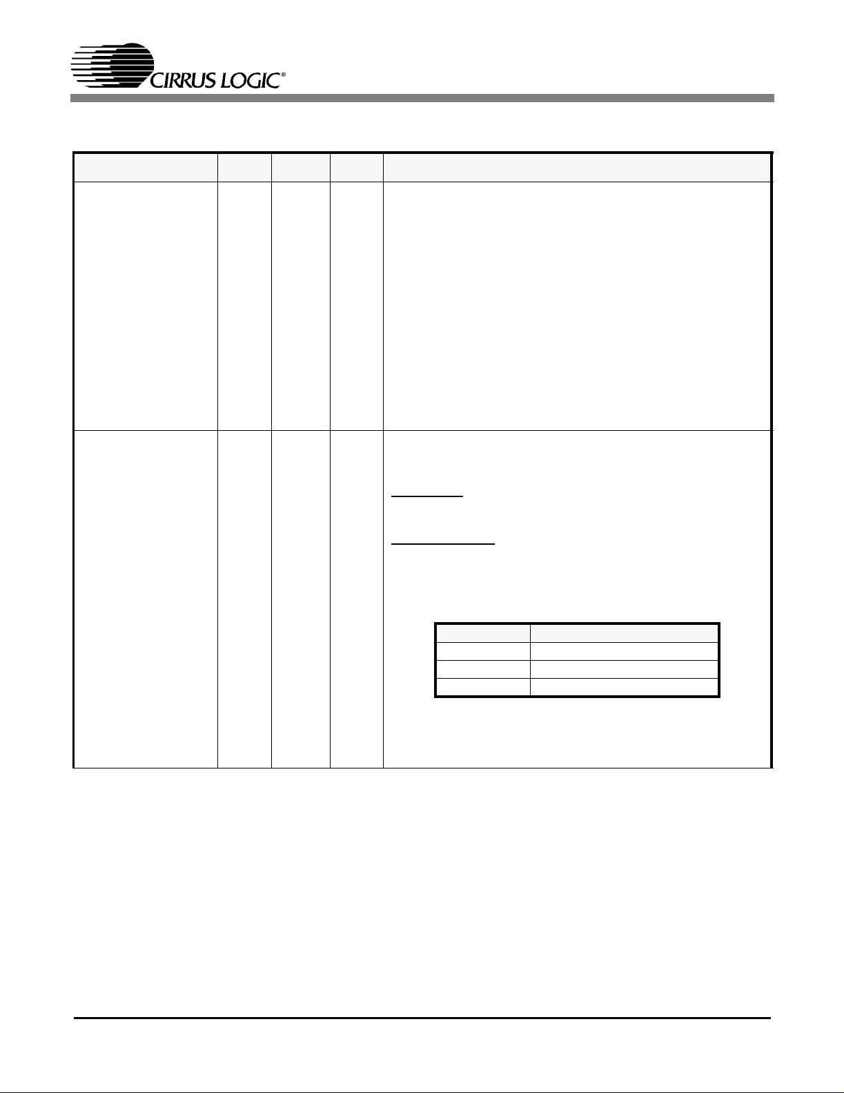
Octal E1 Line Interface Unit
CS61880
Features
Octal E 1 Short-haul Line Int erface Unit
Low Power
No External Component Changes for 120 Ω / 75 Ω
Operation
Pulse Shapes can be customized by the user
Internal AMI, or HDB3 Encoding/Decoding
LOS Detecti on pe r ITU G.775 or ETS I 300- 233
G.772 Non-Intrusive Monitoring
G.703 BI T S Clock Recovery
Cryst al-less Jit ter Attenuation
Serial/Parallel Microprocessor Control Interfaces
Tra nsmitter Short Circui t Current Limiter ( <50 mA)
TX Drivers with Fast High-Z and Power Down
JT AG Boundary Scan compliant to IEE E 1149.1
144-Pin L QF P or 160-Pin FBGA Package
ORDERING INFORMATION
CS61880-IQ 144-pin LQFP
CS61880-IB 160-pin FBGA
Description
The CS61880 is a full -featured Octal E 1 short-haul LIU
that supports 2.048 Mbps data transmission for both E1
75 Ω and E1 120 Ω applications. Each channel provides
crystal-less jitter attenuation that complies with the most
stringent standards. Each channel also provides internal
AMI/HDB3 encoding/decoding. To support enhanced
system diagnostics, cha nnel z ero can be configured for
G.772 non-intrusive monitoring of any of the other 7
channels’ receive or transmit paths.
The CS61880 makes use of ultra low power matched impedance transmitters and receivers to reduce power
beyond that achieved by traditional driver designs. By
achieving a more precise line match, this technique also
provides superior return loss characteristics. Additionally, the internal line matching circuitry reduces the
external component count. All transmitters have controls
for independent power down and High-Z.
Each receiver provides reliable data recovery wi th over
12 dB of cable atte nuation. The receiver also incorpo rates LOS detection compliant to the most recent
specifications.
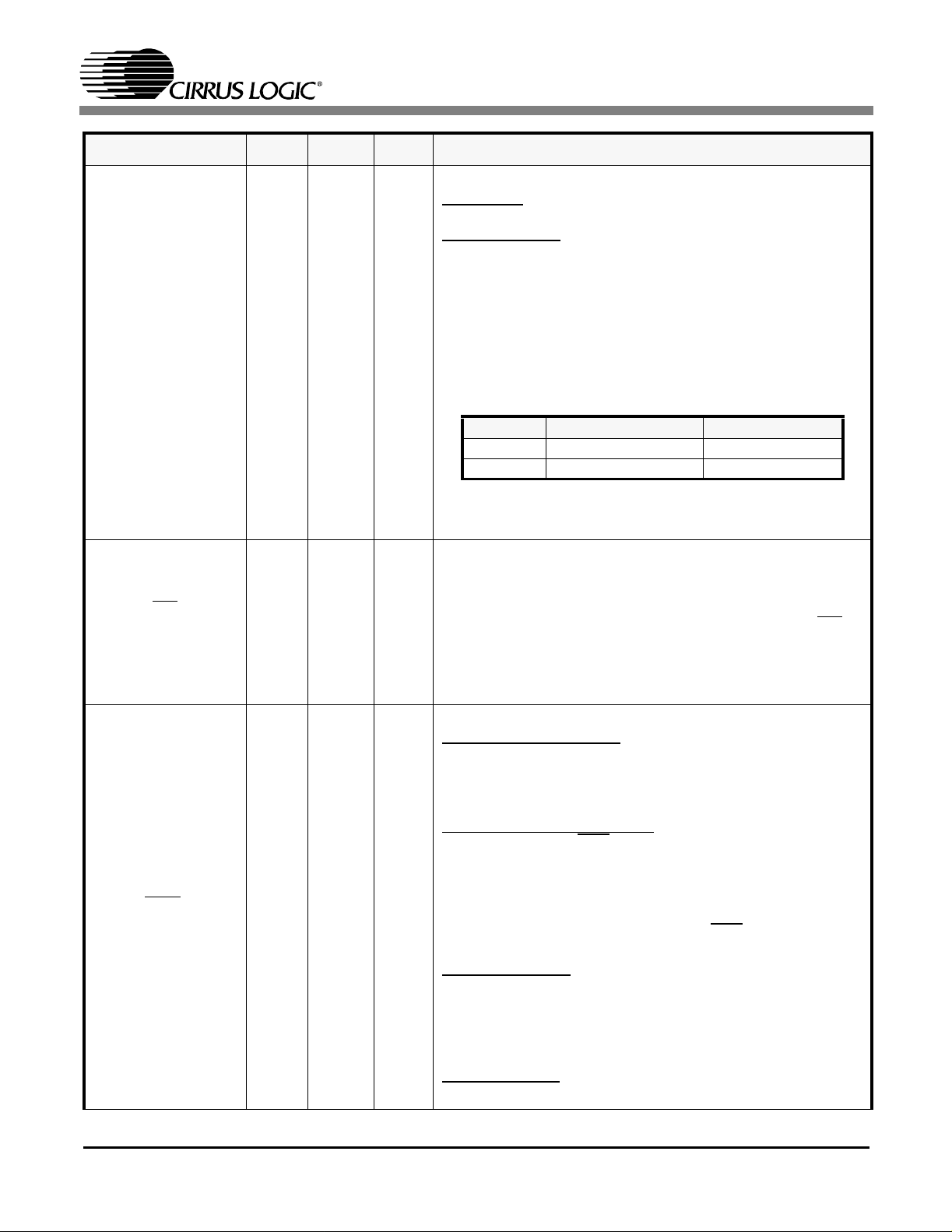
LOS
RCLK
RPOS
RNEG
TCLK
TPOS
TNEG
JTAG
Serial
Port
Decoder
Remote Loopback
Jitter
Attenuator
Encoder
0
1
7
JTAG Interface
Preliminary Product Information
http://www.cirrus.com
LOS
Digital Loopback
This document contains information for a new product.
Cirrus Logic reserves the right to modify this product without notice.
Copyright Cirrus Logic, Inc. 2003
Clock
Recovery
Transmit
Control
(All Rights Reserved)
Recovery
Pulse
Shaper
Host Interface
Data
Receiver
Driver
Analog Loopback
G.772 Monitor
RTIP
RRING
TTIP
TRING
Host
Serial/Parallel
Port
DS450PP3
JUL ‘03
1
Page 2

TABLE OF CONTENTS
1. PIN OUT - 144-PIN LQFP PACKAGE ................................................................................... 7
2. PIN OUT - 160-BALL FBGA PACKAGE ..................................................................................8
3. PIN DESCRIPTIONS ................................................................................................................9
3.1 Power Supplies ........................... .. .......... .. ....... .......... .. ....... ....... ..... ....... ..... ....... .. ..............9
3.2 Control ..................... .......... ......... ................. ......... .......... ................................. ................10
3.3 Address Inputs/Loopbacks ...............................................................................................14
3.4 Cable Select ............ .......... ................................. ......... .......... ................ .......... ......... .......15
3.5 Status ....................... .......... ......... ................. ......... .......... ................ .......... ......... ..............15
3.6 Digital Rx/Tx Data I/O ......................................................................................................16
3.7 Analog RX/T X Dat a I/ O ........ ......... .................................. ......... .......... ................ .......... ....19
3.8 JTAG Test Inter fa ce ............... ................. ......... .......... ................ .......... ......... ...................21
3.9 Miscellaneous .................................................................................................................. 21
4. OPERATION ...........................................................................................................................22
5. POWER-UP .............................................................................................................................22
6. MASTER CLOCK ...................................................................................................................22
7. G.772 MONITORING ..............................................................................................................22
8. BUILDING INTEGRATED TIMING SYSTEMS (BITS) CLOCK MODE ..................................23
9. TRANSMITTER .......................................................................................................................24
9.1 Bipolar Mo d e .......... ......... .......... ................ .......... ......... ................. ......... .......... ................24
9.2 Unipolar Mode .................................................................................................................. 24
9.3 RZ Mode ............................................................... ....... ....... ..... ....... ....... ....... ..... ....... .......25
9.4 Transmit te r Po wer down / High - Z .......... ......... .................................................. ......... .......25
9.5 Transmit All Ones (TAOS) ...............................................................................................25
9.6 Automatic TAOS ............. .......... ................ .......... ......... ................. ......... ........................ ..25
9.7 Driver Failure Monitor ......................................................................................................25
9.8 Driver Short Circuit Protection .........................................................................................25
CS61880
Contacting Cirrus Logic Support
For all product quest ions and inquir ies contact a Cirr us Logi c Sales Representativ e.
To find the one nearest to you go to:
IMPORTANT NOTICE
“Preliminary” product information describes products that are in production, but for which full characterization data is not yet available. Cirrus Logic, Inc. and its
subsidiaries (“Cirrus”) believe that t he information contained in this document is accurate and reliable. However , the infor mation i s subj ect to change without
notice and is provi ded “AS IS” without warranty of any kind (express or implied) . Customers ar e advised to obtain t he lates t versi on of relevant informati on to
verify, before placing orders, that information being relied on is current and complete. All products are sold subject to the terms and conditions of sale supplied
at the time of order acknowledgment, including those pertaining to warranty, patent infringement, and limitation of liability. No responsibility is assumed by Cirrus
for the use of this information, including use of this information as the basis for manufacture or sale of any items, or for infringement of patents or other rights of
third parti es. This document is the property of Cirrus and by furnishing th is information, Cirrus grants no license, express or implied under any patents, mask
work rights, copyrights, trademarks, trade secrets or other intellectual property rights. Cirrus owns the copyrights associated with the information contained herein and gives consent for copies to be made of the information only for use within your organization with respect to Cirrus integrated circuits or other products of
Cirrus. This consent does not extend to other copying such as copying for general distribution, advertising or promotional purposes, or for creating any work for
resale.
An export permit needs to be obtained from the competent authorities of the Japanese Government if any of the products or technologies described in this material and controlled under the “Foreign Exchange and Foreign Trade Law” is to be exported or taken out of Japan. An export license and/or quota needs to be
obtained from the competent authorities of the Chinese Government if any of the products or technologies described in this material is subject to the PRC Foreign
Trade Law and is to be exported or taken out of the PRC.
CERTAIN APPLI CATI ONS USING SEMICONDUCTOR PRODUCTS MAY INVOLVE POTENTI AL RI SKS OF DEATH, PERSONAL I NJURY, OR SEVERE
PROPERTY OR ENVIRONMENTAL DAMAGE (“CRITICAL APPLICATIONS”). CIRRUS PRODUCTS ARE NOT DESIGNED, AUTHORIZED OR WARRANTED
FOR USE IN AIRCRA FT SYSTEMS, MILITARY APPLICATIONS, PRODUCTS SURGICALLY I MPLANTED INTO THE BODY, LIFE SUPPORT PRODUCTS
OR OTHER CRITICAL APPLICATIONS (INCLUDING MEDICAL DEVICES, AIRCRAFT SYSTEMS OR COMPONENTS AND PERSONAL OR AUTOMOTIVE
SAFETY OR SECURITY DEVICES). INCLUSION OF CIRRUS PRODUCTS IN SUCH APPLICATIONS IS UNDERSTOOD TO BE FULLY AT THE CUSTOMER'S RISK AND CIRRUS DISCLAIMS AND MAKES NO WARRANTY, EXPRESS, STATUTORY OR IMPLIED, INCLUDING THE IMPLIED WARRANTIES OF
MERCHANTABILITY AND FITNESS FOR PARTICULAR PURPOSE, WITH REGARD TO ANY CIRRUS PRODUCT THAT IS USED IN SUCH A MANNER. IF
THE CUSTOMER OR CUSTOMER'S CUSTOMER USES OR PERMITS THE USE OF CIRRUS PRODUCTS IN CRITICAL A PPLICATI ONS, CUSTOMER
AGREES, BY SUCH USE, TO FULLY INDEMNIFY CIRRUS, IT S OFFICERS, DIRECTORS, EM PLO YEES, DISTRIBUTORS AND OTHER AGENTS FROM
ANY AND ALL LIABILITY, INCLUDING ATTORNEYS' FEES AND COSTS, THAT MAY RESULT FROM OR ARISE IN CONNECTION WITH THESE USES.
Cirrus Logic, Cirrus, and the Cirrus Logic logo designs are trademarks of Cirrus Logic, Inc. All other brand and product names in this document may be trademarks or service marks of their respective owners.
Intel is a registered trademark of Intel Corporation.
Motorola is a registered trademark of Motorola, Inc.
http://w ww.cirrus.com/
2 DS450PP3
Page 3

CS61880
10. RECEIVER ........................... .......... ......... ................................. .......... ......... ..........................26
10.1 Bipolar Output Mode ............................................................................ ....... ....... ............26
10.2 Unipolar Output Mode ................................................................................................... 26
10.3 RZ Output Mode .............................. ....... ....... ............ ..... ....... ....... ....... ....... ....... .......... ..26
10.4 Receiver Po we rd own/High-Z ................ ......... .......... ......... ................. ......... .......... .........27
10.5 Loss-of-Signal (LOS) ........... ....... ..... ....... ....... .......... .. ....... ....... ..... ....... ....... ....... ..... .......27
10.6 Alarm Indication Signal (AIS) ......................................................................................... 27
11. JITTER ATTENUATOR ........................................................................................................28
12. OPERATIONAL SUMMARY .................. .............................................................................. 29
12.1 Loopbacks ..................................................................................................................... 29
12.2 Analog Loopback ...........................................................................................................29
12.3 Digital Loopback ...................................................................... ............ ....... ....... ............ 30
12.4 Remote Loopback ..................................................... ....... ....... ..... ....... ....... ....... ............30
13. HOST MODE ........................................................................................................................ 32
13.1 SOFTWARE RESET .... ................. ......... .......... ................ .......... ......... ................. .........32
13.2 Serial Po r t Ope ra tion .. ......... ................. ......... .......... ................ .......... ......... ................. ..32
13.3 Parallel Port Operation ..................................................................................................33
13.4 Register Set ........... ................. ......... .......... ................................. ......... .......... ................34
14. REGISTER DESCRIPTIONS ......... ......... .......... ................ .......... ......... .......... ................ ....... 35
14.1 Revision/IDcode Register (00h) .................................................... ....... ....... ..... ....... ..... ..35
14.2 Analog Loopback Register (01h) ...................................................................................35
14.3 Remote Loopback Register (02h) ..................................................................................35
14.4 TAOS Enable Regi ste r (0 3 h) ............................ ......... .......... ................ .......... ......... ....... 35
14.5 LOS Status Register (04h) ................... ......... .................................. ......... ..................... 35
14.6 DFM Status Regi ste r ( 0 5h) ................... .................................................. ......... .......... .... 35
14.7 LOS Interrupt Enable Register (06h) ................................................. ....... .. ....... ..... .......36
14.8 DFM Interrupt Enable Register (07h) ............................................................................ 36
14.9 LOS Interrupt Status Register (0 8 h) ....... ................. ......... .......... ................ .......... .........36
14.10 DFM Interrupt Status Register (09h) ...........................................................................36
14.11 Software Reset Register (0Ah) .................................................................................... 36
14.12 Performance Monitor Register (0Bh) ........................................................................... 36
14.13 Digital Loopback Reset Register (0Ch) .......................................................................36
14.14 LOS/AIS Mode Enable Register (0Dh) ........................................................................ 37
14.15 Automati c TAOS Register (0Eh) ................ ................. ......... .......... ......... ................. .... 37
14.16 Global Control Register (0F h) ............... ................. ......... .......... ...................................37
14.17 Line Length Channel ID Register (10h) ....................................................................... 38
14.18 Line Length Data Register (11h) .................................................................................38
14.19 Output Disable Register (12h) .....................................................................................38
14.20 AIS Status Register (13h) ............................................................................................ 38
14.21 AIS Interrupt Enable Register (14h) ............................................................................ 39
14.22 AIS Interrupt Status Register (15h) ............................................................................. 39
14.23 AWG Broadcast Register (16h) ...................................................................................39
14.24 AWG Phase Address Register (17h) ...........................................................................39
14.25 AWG Phase Data Register (18h) ................................................................................39
14.26 AWG Enable Register (19h) ........................................................................................ 40
14.27 Reserved Register (1Ah) .............................................................................................40
14.28 Reserved Register (1Bh) .............................................................................................40
14.29 Reserved Register (1Ch) ............................................................................................. 40
14.30 Reserved Register (1Dh) ............................................................................................. 40
14.31 Bits Clock Enable Register (1Eh) ............................................... ....... ....... ..... ....... .......40
14.32 Reserved Register (1Fh) ............................................................................................. 40
14.33 Status Registers ..........................................................................................................40
14.33.1 Interrupt Enable Registers ..............................................................................41
DS450PP3 3
Page 4

CS61880
14.33.2 Inter r u pt Sta tu s Re g ist e r s ....................... ......... ......... ......................................41
15. ARBITRARY WAVEFORM GENERATOR ...........................................................................42
16. JTAG SUPPORT .................... ................ .......... ......... .......... ................ .......... ......... .............. 43
16.1 TAP Control ler ............................................. .......... ................................. ......... ..............44
16.1.1 JTAG Reset .......................................................................................................44
16.1.2 Test-Logic-Reset ...............................................................................................44
16.1.3 Run-Test-Idle ....................................................................................................44
16.1.4 Select-DR-Scan ................................................................................................44
16.1.5 Capture-DR .......................................................................................................44
16.1.6 Shift-DR .............................................................................................................44
16.1.7 Exit1-DR ............................................................................................................44
16.1.8 Pause-DR ..........................................................................................................45
16.1.9 Exit2-DR ............................................................................................................45
16.1.10 Update-DR ......................................................................................................45
16.1.11 Select-IR-Scan ................................................................................................45
16.1.12 Capture-IR .......................................................................................................45
16.1.13 Shift-IR ............................................................................................................45
16.1.14 Exit1-IR ...........................................................................................................46
16.1.15 Pause-IR .........................................................................................................46
16.1.16 Exit2-IR ...........................................................................................................46
16.1.17 Update-IR ........................................................................................................46
16.2 Instruction Register (IR) .................................................................................................46
16.2.1 EXTEST ............................................................................................................46
16.2.2 SAMPLE/PRELOAD .........................................................................................46
16.2.3 IDCODE ............................................................................................................46
16.2.4 BYPASS ............................................................................................................46
16.3 Device ID Register (IDR) .......... .......... ...........................................................................47
17. BOUNDARY SCAN REGISTER (BSR) ................................................................................47
18. APPLICATIONS ........................ ......... .......... ................................. .......... ......... .....................50
18.1 Transf ormer Specificat ion s ................... ......... .......... ................ .......... ............................52
18.2 Cryst a l Os c illat o r Specifica tions .... .. .. . .... .............. . .. .... . .. .... . .... .. . .... . .. .... . .. .... . .. .... . .... . .. ... 52
18.3 Line Prote c ti o n ................. ................ .......... ................................. ......... .......... ................ 52
19. CHARACTERISTICS AND SPECIFICATIONS .................................................................... 53
19.1 Absolute Maximum Ratings ...........................................................................................53
19.2 Recommended Operating Conditions . .. .. ....... ............ ....... ....... .......... ....... ....... ....... .......53
19.3 Digital Chara cteristics ........ ......... ...................................................................................54
19.4 Transmitter Analog Characteristics ................................................................................54
19.5 Receiver An a log Chara c teristics ......... ................................................. .......... ......... .......5 5
19.6 Jitter Attenuator Characte r istics ..................... .................................. ......... ......... .......... ..56
19.7 Master Clock Switching Characteristics .........................................................................58
19.8 Transmit Switching Characteristics ................................................................................58
19.9 Receive Swi tch i n g Char ac te r istics .................... ......... .......... ......... .................................58
19.10 Switching Characteristics - Serial Port .........................................................................60
19.11 Switching Characteristics - Parallel Port (Multiplexed Mode) .............................. .......61
19.12 Switching Characteristics- Parallel Port (Non-Multiplexed Mode) ...............................64
19.13 Switching Characteristics - JTAG ................... ......... .......... ..........................................67
20. COMPLIANT RECOMMENDATIONS AND SPECIFIC ATIONS ....... ................ .......... .........68
21. 160-BALL FBGA PACKAGE DIMENSIONS ........................... ... .. .. .......................... ............69
22. 144-PIN LQFP PACKAGE DIMENSIONS .......................................................................70
4 DS450PP3
Page 5

LIST OF FIGURES
Figure 1. CS61880 144-Pin LQFP Package Pin Outs ....................................................................7
Figure 2. CS61880 160-Ball FBGA Package Pin Outs ................................................................... 8
Figure 3. G.703 BITS Clock Mode in NRZ Mode.......................................................................... 23
Figure 4. G.703 BITS Clock Mode in RZ Mode............................................................................. 23
Figure 5. G.703 BITS Clock Mode in Remote Loopback .............................................................. 23
Figure 6. Pulse Ma sk at E1 Inter face......... .......... ......... .................................. ......... ......... ............24
Figure 7. Analog Loopback Block Diagram...................................................................................30
Figure 8. Analog Loopback with TAOS Block Diagram.................................................................30
Figure 9. Digital Loopback Block Diagram................................ ..... ....... ....... ....... ....... ....... ..... .......31
Figure 10. Digital Loopback with TAOS........ ......... ....................................................................... 31
Figure 11. Remote Loopback Block Diagram ..................................................... ..... ....... .. .......... ..31
Figure 12. Serial Read/Write Format (SPOL = 0)......................................................................... 33
Figure 13. Arbitrary Waveform UI.................................................................................................42
Figure 14. Test Acce ss Po r t Arch itecture........... ......... .......... ................................. ......... .......... .... 44
Figure 15. TAP Cont r o lle r Sta te Diag r a m.............. .......... ................ .......... ......... .......... ................45
Figure 16. Internal RX/TX Impedance Matching.................................................................... .......50
Figure 17. Internal TX, External RX Impedance Matching............................................................ 51
Figure 18. Jit te r Tran s fer Chara cteristic vs. G.7 3 6 & TBR 12/13........ ......... .......... ....................... 56
Figure 19. Jitter Tolerance Characteristic vs. G.823..................................................................... 57
Figure 20. Recovered Clock and Data Switching Characteristics................................................. 59
Figure 21. Tran smi t Cloc k and Data Switching Charact e ristics..... ......... .......... ......... .......... .........59
Figure 22. Signal Rise and Fall Characteristics............................................................................ 59
Figure 23. Serial Port Read Timing Diagram................................................................................ 60
Figure 24. Serial Port Write Timing Diagram................................................................................ 60
Figure 25. Parallel Port Timing - Writ e ; In te l® Multiplexed Addre ss / Data Bus Mode .................62
Figure 26. Paral lel Port Timing - Read; Inte l Mul ti p lexed Address / Data Bus Mode....................62
Figure 27. Parallel Port Timing - Write; Motorola® Multiplexed Address / Data Bus Mode .......... 63
Figure 28. Parallel Port Timing - Read; Motorola Multiplexed Address / Data Bus Mode............. 63
Figure 29. Paral lel Port Timing - Write; In te l Non-Multiplexe d Addr e ss / Data Bus Mode.......... ..65
Figure 30. Parallel Port Timing - Read; Intel Non-Multiplexed Address / Data Bus Mode............ 65
Figure 31. Parallel Port Timing - Write; Motorola Non-Multiplexed Address / Data Bus Mode.....66
Figure 32. Parallel Port Timing - Read; Motorola Non-Multiplexed Address / Data Bus Mode. ....66
Figure 33. JTAG Switching Characteristics................................................................................... 67
Figure 34. 160-Ball FBGA Package Drawing.................................................................. .. .......... ..69
Figure 35. 144-Pin LQFP Package Drawing................................................................................. 70
CS61880
DS450PP3 5
Page 6

LIST OF TABLES
Table 1. Operation Mode Selection...............................................................................................10
Table 2. Mux/Bits Clock Selection.................................................................................................11
Table 3. Jitter Attenuation Selection..............................................................................................12
Table 4. Cable Impedance Selection ..................................................................................... .......15
Table 5. Bipolar Mode Translations...............................................................................................16
Table 6. G.772 Address Selection .. ...............................................................................................22
Table 7. Jitter Attenuator Configurations .......................................................................................28
Table 8. Operational Summary .....................................................................................................29
Table 9. Host Control Signal Descriptions.....................................................................................32
Table 10. Host Mode Register Set................................................................................................34
Table 11. Jitter Attenuator Position Selection ...............................................................................37
Table 12. Transmitter Pulse Shape Selection...............................................................................38
Table 13. JTAG Instructions..........................................................................................................46
Table 14. Boundary Scan Register ...............................................................................................47
Table 15. Trans fo r mer Sp e cifications.. .......... ......... ................. ......... .......... ................ .......... .........52
Table 16. 144-Pin Package Dimensions .......................................................................................70
CS61880
6 DS450PP3
Page 7
1. PIN OUT - 144-PIN LQFP PACKAGE
TNEG7/UBS7
RCLK7
RPOS7/RDATA7
RNEG7/BPV7
LOS7
RTIP7
RRING7
TV+7
TTIP7
TRING7
TGND7
RRING6
RTIP6
TGND6
TRING6
TTIP6
144
143
142
140
139
138
137
136
135
134
133
132
131
130
129
CS61880
144-Pin
LQFP
(Top View)
TPOS7/TDATA7
TCLK7
LOS6
RNEG6/BPV6
RPOS6/RDATA6
RCLK6
TNEG6/UBS6
TPOS6/TDATA6
TCLK6
MCLK
MODE
A4
A3
A2
A1
A0
VCCIO
GNDIO
RV0+
RGND0
LOOP0/D0
LOOP1/D1
LOOP2/D2
LOOP3/D3
LOOP4/D4
LOOP5/D5
LOOP6/D6
LOOP7/D7
TCLK1
TPOS1/TDATA1
TNEG1/UBS1
RCLK1
RPOS1/RDATA1
RNEG1/BPV1
LOS1
TCLK0
141
1
2
3
4
5
6
7
8
9
10
11
12
13
14
15
16
17
18
19
20
21
22
23
24
25
26
27
28
29
30
31
32
33
34
35
36
CS61880
TV+6
RTIP5
RRING5
TV+5
TTIP5
TRING5
TGND5
RRING4
RTIP4
TGND4
TRING4
TTIP4
TV+4
CLKE
TXOE
LOS4
RNEG4/BPV4
RPOS4/RDATA4
RCLK4
TNEG4/UBS4
120
118
116
115
114
113
112
111
110
127
126
125
124
123
122
121
119
128
117
109
108
107
106
105
104
103
102
101
100
TPOS4/TDATA4
TCLK4
LOS5
RNEG5/BPV5
RPOS5/RDATA5
RCLK5
TNEG5/UBS5
TPOS5/TDATA5
99
98
97
96
95
94
93
92
91
90
89
88
87
86
85
84
83
82
81
80
79
78
77
76
75
74
73
TCLK5
TDI
TDO
TCK
TMS
TRST
REF
CBLSEL
VCCIO
GNDIO
RV1+
RGND1
INTL/MOT/CODEN
CS/JASEL
ALE/AS/SCLK
RD/RW
WR/DS/SDI
RDY/ACK/SDO
INT
TCLK2
TPOS2/TDATA2
TNEG2/UBS2
RCLK2
RPOS2/RDATA2
RNEG2/BPV2
LOS2
TCLK3
TPOS3/TDATA3
373839
RCLK0
TNEG0/USB0
TPOS0/TDATA0
4142434445
40
LOS0
RNEG0/BPV0
RPOS0/RDATA0
MUX/BITSEN0
47
46
484950
51525354555657
TV+0
TTIP0
RTIP0
TGND0
TRING0
RRING0
TGND1
TV+1
TTIP1
TRING1
RRING1
585960616263646566676869707172
TV+2
TTIP2
RTIP1
RTIP2
TGND2
TRING2
RRING2
TGND3
TV+3
TTIP3
TRING3
LOS3
RTIP3
RRING3
RNEG3/RBPV3
RPOS3/RDATA3
RCLK3
TNEG3/UBS3
Figure 1. CS61880 144-Pin LQFP Package Pin Outs
DS450PP3 7
Page 8
2. PIN OUT - 160-BALL FBGA PACKAGE
CS61880
1234567891011121314
A
B
C
D
E
F
G
H
K
LOS
A3
A0
RPOS
7
TPOS
7
RPOS
6
TPOS
6
MODE
6
LOOP
RCLK
7
TCLK
7
RCLK
6
TCLK
6
MCLK
A2
VCCIO
0
A
7
B
7
C
6
D
6
E
A1
F
G
RCLK
4
TCLK
4
RCLK
5
TCLK
5
TXOE
TCK
VCCIO
RPOS
4
TPOS
4
RPOS
5
TPOS
5
CLKE
TDO
CBLSEL
RNEG
4
TNEG
4
RNEG
5
TNEG
5
LOS
5
TDI
TRST
TVCC
4
TVCC
4
TVCC
5
TVCC
5
LOS
4
TMS
GNDIO
TRING
4
TTIP
4
TRING
5
TTIP
5
TGND
4
TGND
4
TGND
5
TGND
5
RTIP
RRING
RTIP
RRING
RTIP
4
4
5
5
7
RRING
7
RTIP
6
RRING
6
CS61880
TGND
7
TGND
7
TGND
6
TGND
6
TRING
7
TTIP
7
TRING
6
TTIP
6
TVCC
7
TVCC
7
TVCC
6
TVCC
6
LOS
7
A4
GNDIO
RNEG
TNEG
RNEG
TNEG
160 FBGA
RV1+
WR
J
RDY
REF
RD
INT
INTL
ALE
LOS
RGND
1
CS
LOS
2
3
(Bottom View)
RGND
LOOP
0
3
LOS
0
LOOP
LOOP
LOS
LOOP
1
LOOP
4
MUX
1
RV0+
2
LOOP
5
LOOP
H
J
6
K
7
TPOS
2
RPOS
2
TPOS
3
RPOS
3
TNEG
2
RNEG
2
TNEG
3
RNEG
3
TVCC
2
TVCC
2
TVCC
3
TVCC
3
TTIP
2
TRING
2
3
TRING
3
2
2
TTIP
3
3
TGND
TGND
TGND
TGND
RRING
2
2
RRING
3
3
2
RTIP
2
3
RTIP
3
RRING
1
RTIP
1
RRING
0
RTIP
0
TGND
1
TGND
1
TGND
0
TGND
0
TTIP
1
TRING
1
TTIP
0
TRING
0
TVCC
1
TVCC
1
TVCC
0
TVCC
0
TNEG
1
RNEG
1
TNEG
0
RNEG
0
TPOS
1
RPOS
1
TPOS
0
RPOS
0
TCLK
1
RCLK
1
TCLK
0
RCLK
0
L
M
N
P
M
TCLK
L
RCLK
TCLK
N
RCLK
P
1234567891011121314
Figure 2. CS61880 160-Bal l FB GA Package Pin Outs
8 DS450PP3
Page 9
3. PIN DESCRIPTIONS
3.1 Power Supplies
SYMBOL LQFP FBGA TYPE DESCRIPTION
CS61880
17
VCCIO
GNDIO 18
RV0+
RV1+
RGND0
RGND1
TV+0 44 N4, P4 Power Supply, Transmit Driver 0
TGND0 47 N6, P6 Ground, Transmit Driver 0
TV+1 53 L4, M4 Pow er S upp ly, Transmit Driver 1
TGND1 50 L6, M6 Ground, Transmit Driver 1
TV+2 56 L11
TGND2 59 L9, M9 Ground, Transmit Driver 2
TV+3 65 N11
92
91
19
90
20
89
G1
G14
G4
G11
H1
H14
H4
H11
M11
P11
Power Supply, Digital Interface: Power supply for digital
interface pins; typically 3.3 V
Ground, Digital Interface:
Power supply ground for the digital interface; typically 0 V
Power Supp ly, Core Circuitry: Power supply for all sub-cir-
cuits except the transmit driver; typically +3.3 V
Ground , Core Circuitry:
Ground for sub-circuits except the TX driver; typically 0 V
Power supply for transmit driver 0; typically +3.3 V
Power supply ground for transmit driver 0; typically 0 V
Power Supply, Transmit Driver 2
Power Supply, Transmit Driver 3
TGND3 62 N9, P9 Ground, Transmit Driver 3
TV+4 116 A11
B11
TGND4 119 A9, B9 G rou nd , Transmit Driver 4
TV+5 125 C11
D11
TGND5 122 C9,
D9
TV+6 128 C4,
D4
TGND6 131 C6,
D6
TV+7 137 A4, B4 Pow er S upply, Transmit Driver 7
TGND7 134 A6, B6 Ground, Transmit Driver 7
DS450PP3 9
Power Supply, Transmit Driver 4
Power Supply, Transmit Driver 5
Ground, Transmit Driver 5
Power Supply, Transmit Driver 6
Ground, Transmit Driver 6
Page 10
3.2 Control
SYMBOL LQFP FBGA TYPE DESCRIPTION
MCLK 10 E1 I
MODE 11 E2 I
CS61880
Master Clock Input
This pin is a free running reference clock that sh ould be
2.048 MHz. This timing reference is used as follows:
- Timing reference for the clock recovery and jitter attenuation circuitry.
- RCLK reference during Loss of Signal (LOS) conditions
- Transmit clock reference during Transmit all Ones (TAOS)
condition
- Wait state timing for microprocessor interface
- When this pin is held “High”, the PLL clock recovery circuit is disabled. In this mode, the CS61880 rece ivers
function as simple data slicers.
- When this pin is held “Low”, the receiver paths are powered down and the output pins RCLK, RPO S, and RNEG
are High-Z.
Mode Select
This pin is used to select whether the CS61880 operates in
Serial host, Parallel host or Hardware mode.
Host Mode
serial or a parallel microprocessor interface (Ref er to HOST
MODE (See Section 13 on page 32).
Hardware Mode
and the device control/status are provided through the pi ns
on the device.
- The CS61880 is controlled through either a
- The microprocessor interface is disabled
Table 1. Operation Mode Selection
Pin State OPERATING Mode
LOW Hardware Mode
HIGH Parallel Host Mode
VCCIO/2 Serial Host Mode
NOTE: For serial host mode connect this pin to a resistor
divider consi sting of two 10 kΩ res istors between
VCCIO and GNDIO.
10 DS450PP3
Page 11
SYMBOL LQFP FBGA TYPE DESCRIPTION
Multiplexed Interface/Bits Clock Select
MUX/BITSEN0 43 K2 I
Host Mode
face for multiplexed or non-multiplexed operation.
Hardware mode
a G.703 BITS Clock recovery channel (Refer to BUILDING
INTEGRATED TIMING SYSTEMS (BITS) CLOCK MODE
(See Section 8 on page 23). Channel 1 through 7 are not
affected by this pin during hardware mode. During host
mode the G.703 BITS Clock recovery function is enabled by
the Bits Clock Enable Register (1Eh) (See Section 14.31
on page 40).
Pin St a t e Parallel Host Mode Hardware Mode
NOTE: The MUX pin only controls the BITS Clock function in
-This pin configures the microproces sor inter-
- This pin is used to enable channel 0 as
Table 2. Mux/Bits Clock Selection
HIGH multiplexed BITS Clock ON
LOW non multiplexed BITS Clock OFF
Hardware Mode
CS61880
INT
RDY/ACK
82 K13 O
/SDO 83 K14 O
Interrupt Output
This active low output signals the host processor when one
of the CS61880’s internal status register bits has changed
state. When the status register is read, the interrupt is
cleared. The various status changes that would force INT
active are maskable via internal interrupt enable registers.
NOTE: This pin is an open drain output and requires a 10 kΩ
pull-up resistor.
Ready/Data Transfer Acknowledge/Serial Data Output
Intel Parallel Host Mode
access, RDY is asserted “Low” to acknowledge that the device has been accessed. An asserted “High” acknowledges
that data has been written or read. Upon completion of the
bus cycle, this pin High-Z.
Motorola P arallel Host Mo de
operation this pin, “ACK
data on the bus is valid. An asserted “Low” on this pin during a write operation acknowledges that a data transfer to
the addressed register has been ac cepted. Upon completion of the bus cycle, this pin High-Z.
NOTE: Wait state generation via RDY/ACK
RZ mode (No Clock Recovery).
Serial Host Mode
configured for serial bus operation, “SDO” is used as a serial data output. This pin is forced into a high impedance
state during a serial write access. The CLKE pin controls
whether SDO is valid on the rising or falling edge of SC LK.
Upon completion of the bus cycle, this pin High-Z.
Hardware Mode
open.
- When the microprocessor interface is
- This pin is not used and should be left
- During a read or write register
- During a data bus read
”, is asserted “High” to indicate that
is disabled in
DS450PP3 11
Page 12
SYMBOL LQFP FBGA TYPE DESCRIPTION
Write Enable/Data Strobe/Serial Data
WR/DS/SDI 84 J14 I
RD
/RW 85 J13 I
ALE/AS
/SCLK 86 J12 I
Intel Parallel Host Mode
a write enable.
Motorola Parallel Host Mode
a data strobe input.
Serial Host Mode
data input.
Hardware Mode
nected to ground.
Read Enable/Read/Write
Intel Parallel Host Mode
read enable.
Motorola P arallel Host Mo de
as the read/write input signal.
Hardware Mode
nected to ground.
Address Latch Enable/Add ress Strobe/Serial Clock
Intel Parallel Host Mode
Address Latch Enable when co nfigured for multiplexed address/data operation.
Motorola Para llel H ost Mo de
the active “low” address strobe when configured for multiplexed address/data operation.
Serial Host Mode
used for data I/O on SDI and SDO.
Hardware Mode
nected to ground.
- This pin, “SDI”, functions as the serial
- This pin is not used and should be con-
- This pin is not used and should be con-
- This pin, “SCLK”, is the serial clock
- This pin is not used and should be con-
- This pin, “WR”, functions as
- This pin, “DS“, functions as
- This pi n, “R D”, func tions as a
- This pin, “R/W”, functions
- This pin, “ALE”, functions as the
- This pin, “AS”, fun ctio ns as
CS61880
/JASEL 87 J11 I
CS
Chip Select Input/Jitter Attenuator Select
Host Mode
cesses to the microprocessor interface in either serial or
parallel mode.
Hardware Mode
Attenuator.
- This active low input is used to enable ac-
- This pin controls the positio n of the Jitter
Table 3. Jitter Attenuation Selection
Pin State Jitter Attenuation Position
LOW Transmit Path
HIGH Receive Path
OPEN Disabled
12 DS450PP3
Page 13
SYMBOL LQFP FBGA TYPE DESCRIPTION
Intel/Motorola/Coder Mode Select Input
INTL/MOT/CODEN 88 H12 I
TXOE 114 E14 I
Parallel Host Mode
cessor interface is configured for operation with Motorola
processors. When this pin is “High” the microprocessor interface is configured for operation with Intel processors.
Hardware Mode
polar operation, this pin, CODEN
encoding/decoding function. Whe n CODEN
encoders/decoders are enabled. Whe n CODEN
AMI encoding/decoding is ac tivated. This is done for all
eight channels.
Transmitter Output Enable
Host mode
dividual drivers can be set to a high impeda nce state via
the Ou tput Disable Register (12h) (See S ection 14.19 on
page 38).
Hardware Mode
TX drivers are forced into a high impedance state. All other
inter nal cir cuitr y rem ain s acti ve .
- Operates the same as in hardware mode. In-
- When this pin is “Low” the micropro-
- When the CS61880 is configured for uni-
- When TXOE pin is asserted Lo w, all the
CS61880
, configures the line
is low, HDB3
is high,
CLKE 115 E13 I
Clock E dge S elec t
In clock/ data recover y mode , setting CL KE “high” will cause
RPOS/RNEG to be valid on the falling edge of RCLK and
SDO to be valid on the rising edge of SCLK. When CLKE is
set “low”, RPOS/RNEG is v alid on the rising edge of RCLK,
and SDO is valid on the falling edge of SC LK. When the
part is operated in data recovery mode, the RPOS/RNEG
output polarity is active “high” when CLKE is set “high” and
active “low” when CLKE is set “low”.
DS450PP3 13
Page 14
3.3 Address Inputs/Loopbacks
SYMBOL LQFP FBGA TYPE DESCRIPTION
A4 12 F4 I
A3
A2
A1
A0
13
14
15
16
F3
F2
F1
G3
CS61880
Address Selector Input
Parallel Host Mode
mode operation, this pin function as the address 4 input for
the parallel interface.
Hardware Mode
Non-Intr usive Mo nitoring /Addre ss Selecto r Inputs
Parallel Host Mode
mode operation, these pins funct ion as address A[3:0] inputs for the parallel interface.
Hardware Mode
tion during non-intrusive monitoring. In non-intrus ive
I
monitoring mode, receiver 0’s input is internally connected
to the transmit or receive ports on one of the other 7 chan-
I
nels. The recovered clock and data from the sele cted port
are output on RPOS0/RNEG0 and RCLK0. Additionally, the
I
data from the selected port can be output on
TTIP0/TRING0 by activating the remote loopback function
I
for channel 0 (Refer t o Performan ce Monitor Register
(0Bh) (See Section 14.12 on page 36).
- During non-multiplexed parallel host
- The A4 pin must be tied low at all times.
- During non-multiplexed parallel host
- The A[3:0] pins are used for port selec-
LOOP0/D0
LOOP1/D1
LOOP2/D2
LOOP3/D3
LOOP4/D4
LOOP5/D5
LOOP6/D6
LOOP7/D7
21
22
23
24
25
26
27
28
G2
H3
H2
J4
J3
J2
J1
K1
I/O
I/O
I/O
I/O
I/O
I/O
I/O
I/O
Loopback Mode Selecto r/Parallel Data Input/Output
Parallel Host Mode
terface mode, these pins function as the bi-directional 8-bit
data port. When operating in multiplexed microproc essor interface mode, these pins function as the address and data
inputs/outputs.
Hardware Mode
- No Loopback - The CS61880 is in a norm al operating
state when LOOP is left open (unconnected) or tied to
VCCIO/2.
- Local Loopback - When LOOP is tied High, data transmitted on TTIP and TRING is loo ped back into the analog
input of the corresponding channel’s receiver and output on
RPOS and RNEG. Input Data present on RTIP and RRING
is ignored.
- Remote Loopback - When LOOP is tied Low the recovered clock and data received on RTIP and RRING is looped
back for transmission on TTIP and TRI NG. Data on TPOS
and TNEG is ignored.
- In non-multiplexed microprocessor in-
14 DS450PP3
Page 15
3.4 Cable Select
SYMBOL LQFP FBGA TYPE DESCRIPTION
CBLSEL 93 G13 I
CS61880
Cable Impedan ce Sele ct
Host Mode
normal operation.
Hardware Mode
pulse shape and set the line imped ance for all eight receivers and transmitters. This pin also selects whether or not all
eight receivers use an internal or external line matching
network (Refer to the Table 4 below for proper settings).
CBLSEL Transmitters Recei vers
No Connect 120 Ω Internal 120 Ω Internal or External
HIGH 75 Ω Internal 75 Ω Internal
LOW 75 Ω Internal 75 Ω External
- The input voltage to this pin does not effect
- This pin is used to select the transmitted
Table 4. Cable Impedance Selection
3.5
NOTE: Refer to Figure 16 on page 50 and Figure 17 on
page 51 for a ppropriate extern al line matchin g com-
ponents. All transmitters use intern al matching networks.
Status
SYMBOL LQFP FBGA TYPE DESCRIPTION
Loss of Signal Output
LOS0
LOS1
LOS2
LOS3
LOS4
LOS5
LOS6
LOS7
42
35
75
68
113
106
3
140
K4
K3
K12
K11
E11
E12
E3
E4
O
O
The LOS output pins can be c onfigured to indi cate a loss of
O
signal (LOS) state that is compliant to either ITU G.775 or
O
ETSI 300 233. These pins are ass erted “High” to indicate
O
LOS. The LOS output returns low wh en an input signal is
O
present for the time period dictated by the associated speci-
O
fication (Refer to Loss-of-Signal (LOS) (See Section 10.5
O
on page 27)).
DS450PP3 15
Page 16
3.6 Digital Rx/Tx Data I/O
SYMBOL LQFP FBGA TYPE DESCRIPTION
TCLK0 36 N1 I
CS61880
Transmit Clock Input Port 0
- When TCLK is active, the TPOS an d TNEG pins function
as NRZ inputs that are sampled on the falling edge of
TCLK.
- If MCLK is active, TAOS will be generated when TCLK is
held High for 16 MCLK cycles.
NOTE: MCLK is used as the timing reference during TAOS
and mus t hav e th e ap pr o pr iat e sta b ilit y.
- If TCLK is held High in the absence of MCLK, the T POS
and TNEG inputs function as RZ inputs. In this mode, the
transmit pulse width is set by the pulse-width of the signal
input on TPOS and TNEG. To enter this mode, TCLK m ust
be held high for at least 12 µs.
- If TCLK is held Low, the output drivers enter a low-power,
high impedance state.
Transmit Positive Pulse/Transmit Data Input Port 0
Transmit Negative Pulse/Unipolar-Bipolar Select Port 0
The function of the TPOS/TDATA and TNEG/UBS inputs
are determined by whether Unipolar, Bipolar or RZ input
mode has been selected.
Bipolar Mode
TNEG are sampled on the falling edge of TCLK and transmitted onto the line at TTIP and TR ING respectively. A
“High” input on TPOS results in transmission of a positive
pulse; a “High” input on TNEG results in a transmission of a
negative pulse. The translation of TPOS /TNEG inputs to
TTIP/TRING outputs is as follows:
- In this mode, NRZ data on TPOS and
TPOS0/TDATA0
TNEG0/UBS
16 DS450PP3
37
38
N2
N3
I
I
Unipolar mode
TNEG/UBS “High” for more than 16 TCLK cycles, when
MCLK is present. The falling edge of TCLK samples a unipolar data steam on TPOS/TDATA.
RZ Mode
absence of MCLK. In this mod e, the duty cycle of the
TPOS and TNEG inputs determine th e pulse width of the
output signal on TTIP and TRING.
Table 5. Bipolar Mode Translations
TPOS TNEG OUTPUT
0 0 Space
1 0 Positive Mark
0 1 Negative Mark
1 1 Space
- Unipolar mode is activated by holding
- To activate RZ mode tie TCLK “High” in the
Page 17
SYMBOL LQFP FBGA TYPE DESCRIPTION
Receive Clock Output Port 0
- When MCLK is active, this pin outputs the recovered clock
from the signal input on RTIP and RRING. In the event of
LOS, the RCLK output transitions from the rec overed clock
RCLK0 39 P1 O
RPOS0/RDATA0
RNEG0/BPV0
40
41
P2
P3
to MCLK.
- If MCLK is held “High”, the clock recovery circuitry is disabled and the RCLK output is driven by the XO R of RNEG
and RPOS.
- If MCLK is held “Low”, this output is in a high-impedance
state.
Receive Positive Pulse/ Receive Data Output Port 0
Receive Negative Pulse/Bipolar Violation Outpu t Port 0
The function of the RPOS/RDATA and RNEG/BPV outputs
are determined by whether Unipolar, Bipolar, or RZ input
mode has been selected. During LOS , the RPOS/RNEG
outputs will remain active.
NOTE: The RPOS/RNEG ou tputs can be High-Z by hold ing
MCLK Low.
Bipolar Output M ode
O
tion, NRZ Data is recovered from RTIP/RRING and output
on RPOS/RNEG. A high signal on RPOS or RNEG corre-
O
spond to the receipt of a positive or negative pulse on
RTIP/RRING respectively. The RPOS/RNEG outputs are
valid on the falling or rising edge of RCLK as configured by
CLKE.
Unipolar Output Mode
the recovered data is output on RDATA. The decoder signals bipolar violations are output on the RNEG/BPV pin.
RZ Output Mode
output RZ data recovered by slicing the signal present on
RTIP/RRING. A positive pulse on RTIP with respect to
RRING generates a logic 1 on RPOS; a positive pulse on
RRING with respect to RTIP generates a logic 1 on RNEG.
The polarity of the output on RPOS/RNE G is selectable using the CLKE pin. In this mode, external circuitry is used to
recover clock from the received signal.
- When configured for Bipolar opera-
- When unipolar mode i s a ctivated,
- In this mode, the RPOS/RNEG pins
CS61880
TCLK1 29 L1 I Transmit Clock Input Port 1
TPOS1/TDATA1 30 L2 I Transmit Positive Pulse/Transmit Data Input Port 1
TNEG1/UBS1 31 L3 I Transmit Negative Pulse/Unipolar-Bipolar Select Port 1
RCLK1 32 M1 O Receive Clock Output Port 1
RPOS1/RDATA1 33 M2 O Receive Positive Pulse/ Receive Data Output Port 1
RNEG1/BPV1 34 M3 O Receive Negative Pulse/Bipolar Violation Output Port 1
TCLK2 81 L14 I Transmit Clock Input Port 2
TPOS2/TDATA2 80 L13 I Transmit Positive Pulse/Transmit Data Input Port 2
TNEG2/UBS2 79 L12 I Transmit Negative Pulse/Unipolar-Bipolar Select Port 2
DS450PP3 17
Page 18

CS61880
SYMBOL LQFP FBGA TYPE DESCRIPTION
RCLK2 78 M14 O Receive Clock Output Port 2
RPOS2/RDATA2 77 M13 O Rec eive Positive Pulse/ Receive Data Output Port 2
RNEG2/BPV2 76 M12 O Receive Negative Pulse/Bipolar Violation Output Po rt 2
TCLK3 74 N14 I Transmit Clock Input Port 3
TPOS3/TDATA3 73 N13 I Transmit Positive Pulse/Transmit Data Input Port 3
TNEG3/UBS3 72 N12 I Transmit Negative Pulse/Unipolar-Bipolar Select Po rt 3
RCLK3 71 P14 O Receive Clock Output Port 3
RPOS3/RDATA3 70 P13 O Receive Positive Pulse/ Receive Data Output Port 3
RNEG3/BPV3 69 P12 O Receive Negative Pulse/Bipolar Violation Output Port 3
TCLK4 107 B14 I Transmit Clock Input Port 4
TPOS4/TDATA4 108 B13 I Transmit Positive Pulse/Transmit Data Input Port 4
TNEG4/UBS4 109 B12 I Transmit Negative Pulse/Unipolar-Bipolar Sele ct Port 4
RCLK4 110 A14 O Receive Clock Output Port 4
RPOS4/RDATA4 111 A13 O Receive Positive Pulse/ Recei ve Data Output Port 4
RNEG4/BPV4 112 A12 O Receive Negative P ulse/Bipolar Violation Output Port 4
TCLK5 100 D14 I Transmit Clock Input Port 5
TPOS5/TDATA5 101 D13 I Transmit Positive Pulse/Transmit Data Input Port 5
TNEG5/UBS5 102 D12 I Transmit Negative Pulse/Unipolar-Bipolar Select Port 5
RCLK5 103 C14 O Receive Clock Output Port 5
RPOS5/RDATA5 104 C13 O Receive Positive P ulse/ Receive Data Output Port 5
RNEG5/BPV5 105 C12 O Receive Negative Pulse/Bipolar Violation Output Po rt 5
TCLK6 9 D1 I Transmit Clock Input Port 6
TPOS6/TDATA6 8 D2 I Transmit Positive Pulse/Transmit Data Input Port 6
TNEG6/UBS6 7 D3 I Transmit Negative Pulse/Unipolar-Bipolar Select Port 6
RCLK6 6 C1 O Receive Clock Output Port 6
RPOS6/RDATA6 5 C2 O Rec eive Positive Pulse/ Receive Data Output Port 6
RNEG6/BPV6 4 C3 O Receive Negative Pulse/ Bipolar Violation Output Port 6
TCLK7 2 B1 I Transmit Clock Input Port 7
TPOS7/TDATA7 1 B2 I Transmit Positive Pulse/Transmit Data Input Port 7
TNEG7/UBS7 144 B3 I Transmit Negative Pulse/Unipolar-Bipolar Select Port 7
18 DS450PP3
Page 19
CS61880
SYMBOL LQFP FBGA TYPE DESCRIPTION
RCLK7 143 A1 O Receive Clock Output Port 7
RPOS7/RDATA7 142 A2 O Receive Po sitive Pulse/ Receive Data Output Port 7
RNEG7/BPV7 141 A3 O Receive Negative Pulse/Bipolar Violation Outpu t Port 7
3.7 Analog RX/TX Data I/O
SYMBOL LQFP FBGA TYPE DESCRIPTION
Transmit Tip Output Port 0
Transmit Ring Output Port 0
These pins are the di fferential outputs of the transmi t driver.
The driver internally matches impedances f or E1 75 Ω or
E1 120 Ω lines requirin g only a 1:1.15 transformer. The
TTIP0
TRING0
45
46
N5
P5
CBLSEL pin is used to select the appropriate line ma tching
O
impedance only in “Hardware” mode . In host mode, the appropriate line matching impedan ce is selected by the Line
O
Length Data Register (11h) (See Section 14.18 on
page 38).
NOTE: TTIP and TRING are forced to a high impedance state
when the TCLK or the TXOE pin is forced “Low”.
Receive Tip Input Port 0
Receive Ring Input Port 0
These pins are the differential line inputs to the receiver.
The receiver uses either Internal Line Impedance or E xternal Line Impedance modes t o match the line impedances
RTIP0
RRING0
TTIP1 52 L5 O Transmit Tip Output Port 1
48
49
P7
N7
for E1 75Ω or E1 120Ω modes.
I
Internal Li ne I mped ance M ode
same external resistors to match the line impedanc e (Refer
I
to Figure 16 on page 50).
External Line Impedance Mode
ent external resistors to match the line impedance (Refer to
Figure 17 on page 51).
- In host mode, the appropriate line impedan ce is selected
by the Line Le ngth Data Reg ister (11h) (See Section
14.18 on page 38).
- In hardware mode, the CBLSEL pin selects the appropriate line impedance. (Refer to Table 4 on page 15 for proper
line impedance settings).
NOTE: Data and clock recovered from the signal input on
these pins are output via RCLK, RPOS, and RNEG.
- The receiver uses the
- The receiver uses differ-
TRING1 51 M5 O Transmit Ring Output Po rt 1
RTIP1 55 M7 I Receive Tip Input Port 1
RRING1 54 L7 I Receive Ring Input Port 1
TTIP2 57 L10 O Transmit Tip Output Port 2
DS450PP3 19
Page 20
SYMBOL LQFP FBGA TYPE DESCRIPTION
TRING2 58 M10 O Transmit Ring Output Port 2
RTIP2 60 M8 I Receive Tip Input Port 2
RRING2 61 L8 I Receive Ring Input Port 2
TTIP3 64 N10 O Transmit Tip Output Port 3
TRING3 63 P10 O Transmit Ring Output Port 3
RTIP3 67 P8 I Receive Tip Input Port 3
RRING3 66 N8 I Receive Ring Input Port 3
TTIP4 117 B10 O Transmit Tip Output Port 4
TRING4 118 A10 O Transmit Ring Output Port 4
RTIP4 120 A8 I Receive Tip Input Port 4
RRING4 121 B8 I Receive Ring Input Port 4
TTIP5 124 D10 O Transmit Tip Output Port 5
CS61880
TRING5 123 C10 O Transmit Ring Output Port 5
RTIP5 127 C8 I Receive Tip Input Port 5
RRING5 126 D8 I Receive Ring Input Port 5
TTIP6 129 D5 O Transmit Tip Output Port 6
TRING6 130 C5 O Transmit Ring Output Port 6
RTIP6 132 C7 I Receive Tip Input Port 6
RRING6 133 D7 I Receive Ring Input Port 6
TTIP7 136 B5 O Transmit Tip Output Port 7
TRING7 135 A5 O Transmit Ring Output Port 7
RTIP7 139 A7 I Receive Tip Input Port 7
RRING7 138 B7 I Receive Ring Input Port 7
20 DS450PP3
Page 21
3.8 JTAG Test Interface
SYMBOL LQFP FBGA TYPE DESCRIPTION
TRST
TMS 96 F11 I
TCK 97 F14 I
TDO 98 F13 O
95 G12 I
CS61880
JTAG Reset
This active Low input resets the JTAG controller. This input
is pulled up internally and may be left as a NC when not
used.
JTAG Test Mode Select Input
This input enables the JTAG serial port when active High.
This input is sampled on the rising edge of TCK . This input
is pulled up internally and may be left as a NC when not
used.
JTAG Test Clock
Data on TDI is valid on the rising edge of TCK. Data on
TDO is valid on the falling edge of T CK. When TCK is
stopped high or low, the contents of all JTAG registers remain unchanged. Tie pin low through a 10 kΩ resistor when
not used.
JTAG Test Data Output
JTAG test data is shifted out of the device on this pin. Data
is output on the fallin g edge of TCK . Leave as NC w hen not
used.
TDI 99 F12 I
3.9 Miscellaneous
SYMBOL LQFP FBGA TYPE DESCRIPTION
REF 94 H13 I Reference Input
JTAG Test Data Input
JTAG test data is shifted into the device using this pin. Th e
pin is sampled on the rising edge of TCK . TDI is pulled up
internally and may be left as a NC when not used.
This pin must be tied to ground through 13. 3 kΩ 1% resistor. This pin is used to set the internal current level.
DS450PP3 21
Page 22

CS61880
4. OPERATION
The CS61880 is a full featured line interface unit
for up to eight E1 75 Ω or E1 120 Ω lines. The device provides an interface to twisted pair or co- axial media. A matched impedance technique is
employed that reduces power and eliminates the
need for matching resistors. As a result, the device
can interface directly to the line through a transformer without the need for matching resistors on
the transmit side. The r eceive side uses the sa me resistor values for all E1 settings.
5. POWER-UP
On power-up, the device is held in a static state until the power supply achieves approximately 70%
of the power supply voltage. Once the power supply threshold is passed, the analog circuitry is calibrated, the control registers are reset to their default
settings, and the various internal state machines a re
reset. The reset/calibration process completes in
about 30 ms.
6. MASTER CLOCK
7. G.772 MONITORING
The receive path of channel zero of the CS61880
can be used to monitor the receive or transmit paths
of any of the other channels. The signal to be monitored is multiplexed to channel zero through the
G.772 Multiplexer. The multiplexer and channel
zero then form a G.772 compliant digital Protected
Monitoring Point (PMP ). When th e PMP is con nected to the channel, the attenuation in the signal path is
negligible across the signal band. The signal can be
observed using RPOS, RNEG, and RCLK of channel zero or by putt ing chan nel zero in rem ote loopback, the signal can be observed on TTIP and
TRING of channel zero.
The G.772 monitoring function is available during
both host mode and hardware mode operation. In
host modes, individual channels are selected for
monitoring via the Performance Monitor Regis-
ter (0Bh) (See Section 14.12 on page 36)). In hard-
ware mode, individual channels are selected
through the A3:A0 pins (Refer to Table 6 below for
address settings).
The CS61880 requires a 2.048 MHz reference
clock with a minimum accuracy of ±100 ppm. This
clock may be supplied from internal system timing
or a CMOS crystal oscillator and input to the
MCLK pin.
The receiver uses MCLK as a refer ence for clock
recovery, jitter attenuation, and the generation of
RCLK during LOS. The trans mitter uses M CLK as
the transmit timing reference during a blue alarm
transmit all ones condition. In addition, MCLK
provides the reference timing for wait state generation.
In systems with a jittered transmit clock, MCLK
should not be tied to the transmit clock, a separate
crystal oscillator should drive the reference clock
input. Any jitter present on the reference clock will
not be filtered by the jitter attenuator and can cause
the CS61880 to operate incorrectly.
Table 6. G.772 Address Selection
Address [A3:A0] Channel Selection
0000 Monitoring Disabled
0001 Receiver Channel # 1
0010 Receiver Channel # 2
001 1 Receiver Channel # 3
0100 Receiver Channel # 4
0101 Receiver Channel # 5
01 10 Receiver Channel # 6
0111 Receiver Channel # 7
1000 Monitoring Disabled
1001 Transmitter Channel # 1
1010 Transmitter Channel # 2
101 1 Transmitter Channel # 3
1 100 Transmitter Channel # 4
1 101 Transmitter Channel # 5
1110 Transmitter Channel # 6
1111 Transmitter Channel # 7
NOTE: In hardware mode the A4 pi n must be tied low
at all times.
22 DS450PP3
Page 23

8. BUILDING INTEGRATED TIMING SYSTEMS (BITS) CLOCK MODE
CS61880
This mode is used to enable one or more channels
as a stand-alone timing recovery unit used for
G.703 Clock Recovery.
In hardware mode, BITS Clock mode is selected by
pulling the MUX pin “HIGH”. This enables only
channel zero as a stand-alone timing recovery unit,
no other channel can be used as a timing recovery
unit.
RCLK
RTIP
CS61880
RPOS
One Receiver
RNEG
RRING
Figure 3. G.703 BITS Clock Mode in NRZ Mode
In host mode, each channel can be setup as an independent G.703 timing recovery unit, through the
Bits Clock Enable Register (1Eh) (See Section
14.31 on page 40), setting the desired bit to “1” enables BITS Clock mode for that channel. The following diagrams show how the BITS clock
function operates.
0.1µF
R1
RECEIVE
LINE
R2
T1 1:2
RCLK
RPOS
RNEG
TCLK
TPOS
TNEG
RCLK
RPOS
CS61880
One Receiver
RNEG
Figure 4. G.703 BITS Clock Mode in RZ Mode
CS61880
One Channel
REMOTE
LOOPBACK
RTIP
RRING
TTIP
TRING
RTIP
RRING
0.1µF
0.1µF
R1
R2
R1
RECEIVE
LINE
R2
T1 1:2
RECEIVE
LINE
T1 1:2
TRANMIT
LINE
T1 1:1.15
Figure 5. G.703 BITS Clock Mode in Remote Loopb ack
DS450PP3 23
Page 24

CS61880
e
P
n
v
9. TRANSMITTER
The CS61880 contains eight identical transmitters
that each use a low power matched impedance driver to eliminate the need for external load matching
resistors, while providing superior return loss. As a
result, the TTIP/TRING outputs can be connected
directly to the transformer allowing one hardware
circuit for E1 120 Ω, and E1 75 Ω applications.
Digital transmit data and clock are input into the
CS61880 through the TPOS/TDATA, TNEG and
TCLK input pins. These pins accept data in one of
three formats: unipolar, bipolar, or RZ. In either
unipolar or bipolar mode, the CS61880 internally
generates a pulse shape compliant to the G.703
mask for E1 (Refer to Figure 6). The pulse shapi ng
applied to the transmit data can be selected in hardware mode or in host mode.
In hardware mode, the line impedance (75 Ω or
120 Ω) and which prestored pulse shape to transmit
(75 Ω or 120 Ω) is selected via the CBLSEL pin for
all eight transmitters.
In host mode, each channel is conf igured independently by writing to the Line Length Channel ID
Register (10h) (See Section 14.17 on page 38),
then writing the desired line length settings to the
LEN[3:0] bits in the Line Length Data Register
(11h) (See Section 14.18 on page 38). The LEN
bits select the pulse shape and line imp edance of
the addressed channel. In host mode, the CBLSEL
pin is not used.
NOTE: If one channel is configured for E1 75 Ω mode,
another channel can be conf igured for E1
120 Ω mode at the same time. This operation is
only allowed in host mode.
The CS61880 also allows the user to customize the
transmit pulse shapes to compensate for non-standard cables, transformers, or protection circuitry.
For further information on the AWG Refer to Ar-
bitrary Waveform Generator (See Section 15 on
page 42).
ercent of
ominal peak
oltage
120
110
100
90
80
50
10
0
-10
-20
Figure 6. Pulse Mask at E1 Interface
269 ns
244 ns
194 ns
Nominal Puls
219 ns
488 ns
For more information on the host mode registers refer to Register Descriptions (See Section 14 on
page 35).
9.1 Bipolar Mode
Bipolar mode provides transparent operation for
applications in which the line coding function is
performed by an external framing device. In this
mode, the falling edge of TCLK samples NRZ data
on TPOS/TNEG for transmission on TTIP/TRING.
9.2 Unipolar Mode
In unipolar mode, the CS61880 is configured such
that transmit data is encoded using HDB3, or AMI
line codes. This mode is activated by holding
24 DS450PP3
Page 25

CS61880
TNEG/UBS “High” for more than 16 TCLK cycles. Transmit data is input to the part via the
TPOS/TDATA pin on the falling edge of TCLK.
When operating the part in hardware mode, the
CODEN pin is used to select between HDB3 or
AMI encoding. During host mode operation, the
line coding is selected via the Li n e Len gt h Chan-
nel ID Register (10h) (See Section 14.17 on
page 38).
NOTE: The encoders/decoders are selected for all
eight channel s in both hardw are and host
mode.
9.3 RZ Mode
In RZ mode, the internal pulse shape circuitry is
bypassed and RZ da ta driven into TPOS/TNEG is
transmitted on TTIP/TRING. In this mode, the
pulse width of the transmitter output is determined
by the width of the RZ signal input to TPOS/TNEG
pins. This mode is ente red when MCLK is inactive
and TCLK is held “High” for at least 12 µs.
9.4 Transmitter Powerdown / High-Z
The transmitters can be forced into a high impedance, low power state by holding TCLK of the appropriate channel low for at least 12 µs or 140
MCLK cycles. In hardware and host mode, the
TXOE pin forces all eight transmitters into a high
impedance state within 1 µs.
In host mode, each transmitter is individually controllable using the Output Disable Register (12h)
(See Section 14.19 on page 38). The TXOE pin can
be used in host mode, but does not effect the contents of the Output Enable Register. This feature is
useful in applications that require redundancy.
In hardware mode, TAOS is activated by pulling
TCLK “High” for more than 16 MCLK cycles.
In host mode, TAOS is generated for a particular
channel by asserting the associated bit in the TAOS
Enable Register (03h) (See Section 14.4 on
page 35).
Since MCLK is the reference clock, it should be of
adequate stability.
9.6 Automatic TAOS
While a given channel is in the LOS condition, if
the corresponding bit in the Automatic TAOS
Register (0Eh) ( See Section 14.15 on page 37) is
set, the device will drive that channel’s TTIP and
TRING with the all ones pattern. This function is
only available in host mode. Refer to Loss-of-Sig-
nal (LOS) (See Section 10.5 on page 27).
9.7 Driver Failure Monitor
In host mode, the Driver Failure Monitor (DFM)
function monitors the output of each channel and
sets a bit in the DFM Status Re gister (05h) (See
Section 14.6 on page 35) if a secondary short circuit is detected between TTIP and TRING. This
generates an interrupt if the respective bit in the
DFM Interrupt Enable Register (07h) (See Sec-
tion 14.8 on page 36) is also set. Any change in the
DFM Status Register (05h) (See Section 14.6 on
page 35) will result in the corresponding bit in the
DFM Interrupt Status Register (09h) (See Sec-
tion 14.10 on page 36) being set. The inter rupt is
cleared by reading the DFM Interrupt Status
Register (09h) (See Section 14.10 on page 36).
9.8 Driver Short Circuit Protection
9.5 Transmit All Ones (TAOS)
When TAOS is activated, continuous ones are
transmitted on TTIP/TRING using MCLK as the
transmit timing reference. In this mode, the TPOS
and TNEG inputs are ignored.
DS450PP3 25
The CS61880 provides driver short circuit protection when current on the secondary exceeds 50 mA
RMS.
Page 26

CS61880
10. RECEIVER
The CS61880 contains eight identical receivers that
utilize an internal matched impedance technique
that provides for the use of a common set of external components for 120 Ω (E1), and 75 Ω (Ε1) operation (Refer to Figure 16 on page 50). This
feature enables the use of a one stuffing option for
all E1 line imp edances. The receiver s can also be
configured to use different external resistors to
match the line impedance for E1 75 Ω or E1 120 Ω
modes (Refer to Figure 17 on page 51).
In hardware mode, the CBLSEL pin is us ed to select the proper line impedance (75 Ω or 120 Ω) and
either internal or external line impedance matching
mode.
In host mode, each receiver’s line impedance is selected individually via the Line Length Channel
ID Register (10h) (See Section 14.17 on page 38)
and bits[3:0] and the LEN[3:0] bits of the Line
Length Data Register (11h) (See Section 14.18 on
page 38). The INT_EXTB bit of the Lin e Length
Data Register (11h) (See Section 14.18 on
page 38) is used to se lect between i nternal or e xternal line impedance matching modes for all eight
channels. The CBLSEL pin is not used in host
mode.
The CS61880 receiver provides all of the circuitry
to recover both data and clock from the data signal
input on RTIP and RRING. The matched impedance receiver is capable of recover ing signals with
12 dB of attenuation (referenced to 2.37 V or 3.0 V
nominal) while providing superior return loss. In
addition, the timing recovery circuit along with the
jitter attenuator provide jitter tolerance that far exceeds jitter specifications (Refer to Figure 19 on
page 57).
The recovered data and clock are output from the
CS61880 on the RPOS/RDATA, RNEG and
RCLK pins. These pins output the data in one of
three formats: bipolar, unipolar, or RZ. The CLKE
pin is used to configure RPOS/RDATA and
RNEG, so that data is valid on either the rising or
falling edge of RCLK. Refer to the CLKE pin description on page 13 for CLKE settings.
10.1 Bipolar Output Mode
Bipolar mode provides a transparent clock/data recovery for applications in which the line decoding
is performed by an external framing device. The recovered clock and data are output on RCLK,
RNEG and RPOS.
10.2 Unipolar Output Mode
In unipolar mode, the CS61880 decodes the recovered data with either HDB3 or AMI line decoding.
The decoded data is output on the RPOS/RDATA
pin. When bipolar violations are detected by the decoder, the RNEG/BPV pin is asserted “high”. This
pin is driven “high” for one RCLK period for every
bipolar violation that is not part of the zero substitution rules. Unipolar mode is entered by holding
the TNEG pin “high” for more than 16 TCLK cycles.
In hardware mode, the HDB3/AMI encoding/decoding is activated via the CODEN pin.
In host mode, Bit 4 of the Line Length Channel
ID Register (10h) (See Section 14.17 on page 38)
is used to select the encoding/decoding for all channels.
10.3 RZ Output Mode
In this mode the RTIP and RRING inputs are sliced
to data values that are output on RPOS and RNEG
pins. This mode is used in applications that have
clock recovery circuitry external to the device. To
support external clock recovery, the RPOS and
RNEG outputs are XORed and output as RCLK.
This mode is entered when MCLK is tied high. The
polarity of the RPOS/RNEG data are controlled by
the CLKE pin. Refer to the CLKE pin description
on page 13 for CLKE settings.
26 DS450PP3
Page 27

CS61880
10.4 Receiver Powerdown/High-Z
All eight receivers are powered down when MCLK
is held low. In addition, this will force the RCLK,
RPOS/RDATA and RNEG outputs into a high impedance state.
10.5 Loss-of-Signal (LOS)
The CS61880 makes use of both analog and digital
LOS detection circ uitry that is compliant to the latest specifications. The LOS condition can be set to
either ITU G.775 or ETSI 300 233. This change is
done through the LOS/AIS Mode Enable Regis-
ter (0Dh) (See Section 14.14 on page 37).
The LOS detector increments a counter each time a
zero is received, and resets the counter each time a
one “mark” is received. Depending on LOS detection mode, the LOS signal is set when a certain
number of consecutive zeros are received. In
Clock/Data recovery mode, this forces the recovered clock to be replaced by MCL K at the RCLK
output. In addition the RPOS/RDATA and RNEG
outputs remain active for the length of the LOS period, except when local and analog loopbacks are
enabled. Upon exiting LOS, the recovered clock replaces MCLK on the RCLK output. In Data recovery mode, RCLK is not replace d by MCLK when
LOS is active. The LOS detection modes are summarized below.
NOTE: G.775 and ETSI 300 23 3 are both available in
host mode, but in hardware mode only ETSI
300 233 is available.
ITU G.775 (E1 Mode Only) - LOS is declared
when the received signal level is less than 200 mV
for 32 consecutive pulse periods (typical). The device exits LOS when the received s ignal achieves
12.5% ones density with no more than 15 consecu-
tive zeros in a 32-bit sliding window and the signal
level exceeds 250 mV.
ETSI 300 233 (E1 Host Mode Only) - The LOS
indicator becomes active whe n the receive signal
level drops below 200 mV for more than 2048
pulse periods (1 ms). The channel exits the LOS
state when the input signal exceeds 250 mV and
has transitions for more than 32 pulse periods
(16 µs). This LOS detection method can only be se -
lected while in host mode.
During host mode operatio n, LOS is reported i n the
LOS Status Monitor Register. Both the LOS pins
and the register bits reflect LOS status in host mode
operation. The LOS pins and status bits are set high
(indicating loss of signal) during reset, power-up,
or channel powered-down.
10.6 Alarm Indication Signal (AIS)
The CS61880 detects all ones alarm condition per
the relevant ITU, and ETSI specif ications. In general, AIS is indicated when the one’s density of the
receive signal exceeds that dictated by the relevant
specification. This feature is only available in host
mode (Refer to LOS/AIS Mode Enable Register
(0Dh) (See Section 14.14 on page 37)).
ITU G.775 AIS (E1 Mode) - The AIS condition is
declared when less than 3 zeros are received within
two consecutive 512-bit windows. The AIS condition is cleared when 3 or more zeros are received in
two consecutive 512-bit windows.
ETSI 300 233 (E1 Mode) - The AIS condition is
declared when less than 3 zeros are received in a
512-bit window. The AIS condition is cleared
when a 512-bit window is received containing 3 or
more zeros.
DS450PP3 27
Page 28

CS61880
11. JITTER ATTENUATOR
The CS61880 internal jitter attenuators can be
switched into either the receive or transmit paths.
Alternatively, it can be removed from both paths to
reduce the propagation delay.
During Hardware mode operation, the location of
the jitter attenuator for all eight channels are controlled by the JASEL pin (Refer to Table 7 for pin
configurations). The jitter attenuator’ s FIFO length
and corner frequency, can not be changed in hardware mode. The FIFO length and corner frequency
are set to 32 bits and 1.25 Hz.
Table 7. Jitter Attenuator Configurations
PIN STATE JITTER ATTENUATOR POSITON
LOW Transmit Path
HIGH Receive Path
OPEN Disabled
During host mode operation, the l o cation of the jitter attenuator for all eight channels are set by bits 0
and 1 in the Line Length Channel ID Register
(10h) (See Section 14.17 on page 38). This register
(0Fh) also configures the jitter attenuator’s FIFO
length (bit 3) and corner frequency (bit 2).
The attenuator consists of a 64-bit FIFO, a narrowband monolithic PLL, and control logic. The jitter
attenuator requires no external crystal. Signal jitte r
is absorbed in the FIFO which is designed to neither overflow nor underflow.
If overflow or underflow is imminent, the jitter
transfer function is altered to ensure that no bit-errors occur. A configuration option is provided to
reduce the jitter attenuator FIFO length from 64
bits to 32 bits in order to reduce pr opagation delay.
The jitter attenuator - 3 dB knee fre quenc y depe nds
on the settings of the Jitter Attenuator FIFO length
and the Jitter Attenuator Corner Frequency, bits 2
and 3, in the Line Length Channel ID Register
(10h) (See Section 14.17 on page 38)). Setting the
lowest corner frequency guarantees jitter attenuation compliance to European specifications TBR
12/13 and ETS 300 011. The jitter attenuator is also
compliant with ITU-T G.735, G.742, and G.783
(Refer to Figure 18 on page 56 and Figure 19 on
page 57).
28 DS450PP3
Page 29
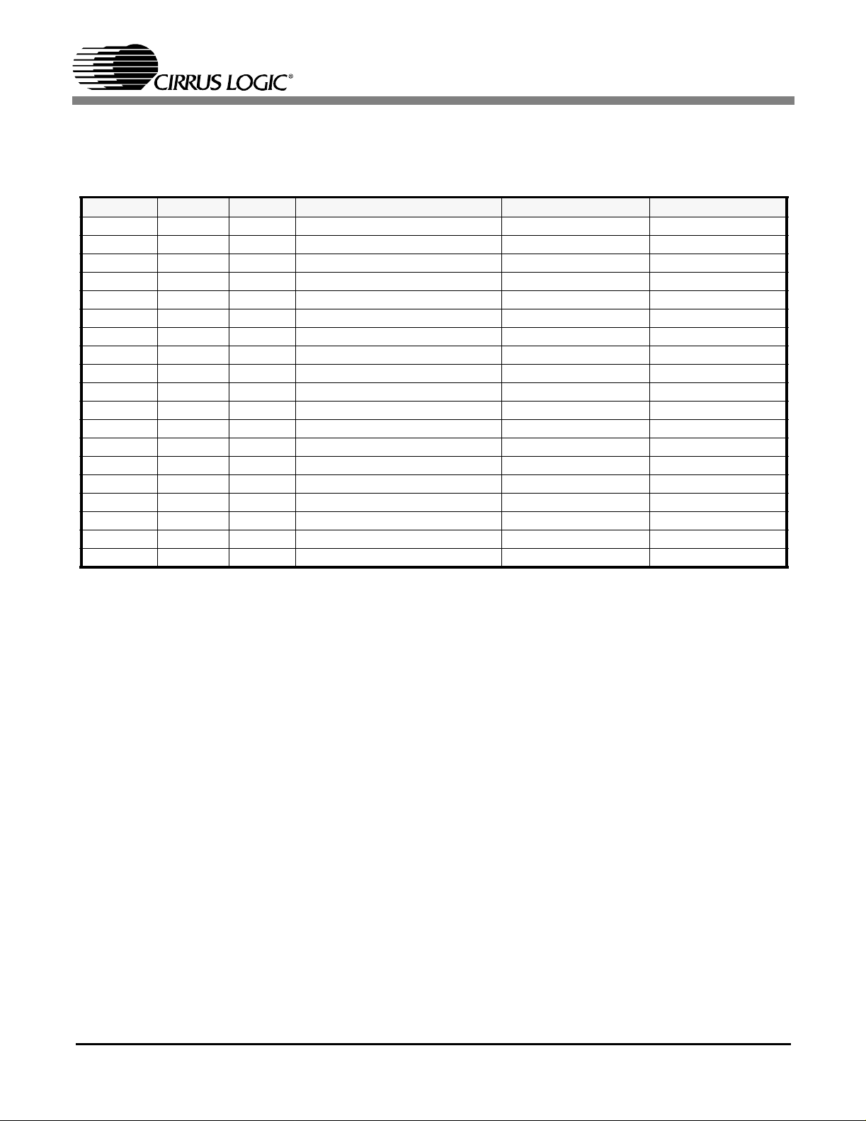
CS61880
12. OPERATIONAL SUMMARY
A brief summary of the CS61880 operations in hardware and host mode is provided in Table 8.
Table 8. Operational Summary
MCLK TCLK LOOP Recei ve Mode Transmit Mode Loopback
Active Active Open RCLK/Data Recovery Unipolar/Bipolar Disabled
Active Active L RCLK/Data Recovery Unipolar/Bipolar Remote Loopback
Active Active H RCLK/Data Recovery Unipolar/Bipolar Analog Loopback
Active L X RC LK/Data Recovery Power Down Disabled
Active H O pen RCLK/Data Recovery TAOS Disabled
Active H L RCLK/Data Recovery Unipolar/Bipolar Rem ote Loopback
Active H H RCLK/Data Recovery TAOS Analog Loopback
L Active X Power Down Unipolar/Bipolar Disabled
L H X Power Down RZ Data Disabled
L L X Power Down Power Down Disabled
H Active Open Data Recovery Unipolar/Bipolar Disabled
H Active L Data Recovery RZ Data Remote Loopback
H Active H Data Recovery Unipolar/Bipolar Analog Loopback
H L O pen Data Recovery Power Down Disabled
H L L Data Recovery RZ Data Remote Loopback
H L H Data Recovery Power Down Disabled
H H O pen Data Recovery RZ Data Disabled
H H L Data Recovery RZ Data Rem ote Loopback
H H H Data Recovery RZ Data Analog Loopback
12.1 Loopbacks
The CS61880 provides three loopback modes for
each port. Analog Loopback connects the transmit
signal on TTIP and TRING to RTIP and RRING.
Digital Loopback Connects the output of the Encoder to the input of the Decoder (through the Jitter
Attenuator if enabled). Remote Loopback connects
the output of the Clock and Data Recovery block to
the input of the Pulse Shaper block. (Refer to detailed descriptions below.) In hard ware mod e, the
LOOP[7:0] pins are used to activate Analog or Remote loopback for each channel. In host mode, the
Analog, Digital and Remote Loopback registers are
used to enable these functions (Refer to the Analog
Loopback Register (01h) (See Section 14.2 on
page 35), Remote Loopback Register (02h) (See
Section 14.3 on page 35), and Digital Loopback
Reset Register (0Ch) (See Section 14.13 on
page 36).
12.2 Analog Loopback
In Analog Loopback, the output of the
TTIP/TRING driver is internally connected to the
input of the RTIP/RRING receiver s o that the data
on TPOS/TNEG and TCLK appears on the
RPOS/RNEG and RCLK outputs. In this mode the
RTIP and RRING inputs are ignored. Refer to
Figure 7 on page 30. In hardware mode, Analog
Loopback is selected by driving LOOP[7:0] high.
In host mode, Analog Loopback is selected for a
given channel using the appropriate bit in the Ana-
log Loopback Register (01h) (See Section 14.2 on
page 35).
NOTE: The simultaneous selection of Analog and
Remote loopbac k modes is n ot valid. A TAOS
request overrides the data on TPOS and TNEG
during Analog Loopbac k. Refer to Figure 8 on
page 30.
DS450PP3 29
Page 30
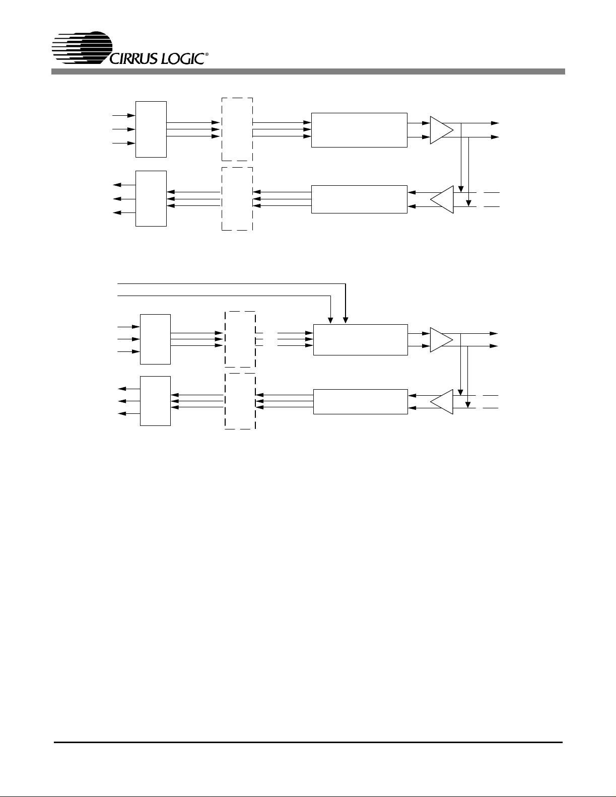
CS61880
TPOS
TNEG
TCLK
RPOS
RNEG
RCLK
MCLK
TAOS
TPOS
TNEG
TCLK
RPOS
RNEG
RCLK
EncoderDecoder
EncoderDecoder
Transmit
Jitter
Attenuator
Jitter
Attenuator
Control &
Pulse Shaper
Clock Recovery &
Data Recovery
Figure 7. Analog Loopba ck Block Diagram
Transmit
Jitter
Attenuator
Jitter
Attenuator
Control &
Pulse Shaper
Clock Recovery &
Data Recovery
TTIP
TRING
RTIP
RRING
TTIP
TRING
(All One's)
RTIP
RRING
Figure 8. Analog Loopback wit h TAOS Block Diagram
12.3 Digital Loopback
Digital Loopback causes the TCLK, TPOS, and
TNEG (or TDATA) inputs to be looped back
through the jitter attenuator (if enabled) to the
RCLK, RPOS, and RNEG (or RDATA) outputs.
The receive line interface is ignored, but data at
TPOS and TNEG (or TDATA) continues to be
transmitted to the line interface at TTIP and
TRING (Refer to Figure 9 on page 31).
Digital Loopback is only available during host
mode. It is selected using the appropriate bit in the
Digital Loopback Reset Register (0Ch) (See Sec-
tion 14.13 on page 36).
NOTE: T AOS can also be used during the Digital Loop-
back operation for the select ed channel (Refer
to Figure 10 on page 31 ).
12.4 Remote Loopback
In remote loopback, the RPOS/RNEG and RCLK
outputs are internally input to the transmit circuits
for output on TTIP/TRING. In this mode the
TCLK, TPOS and TNEG inputs are ignored. (Refer
to Figure 11 on page 31). In hardware mode, Remote Loopback is selected by driving the LOOP
pin for a certain channel low. In host mode, Remote
Loopback is selected for a given channel by writing
a one to the appropriate bit in the Remote Loop-
back Register (02h) (See Section 14.3 on
page 35).
NOTE: In hardware mode, Remote Loopback over-
rides TAOS for the selected channel. In host
mode, TAOS overrides Remote Loopback.
30 DS450PP3
Page 31
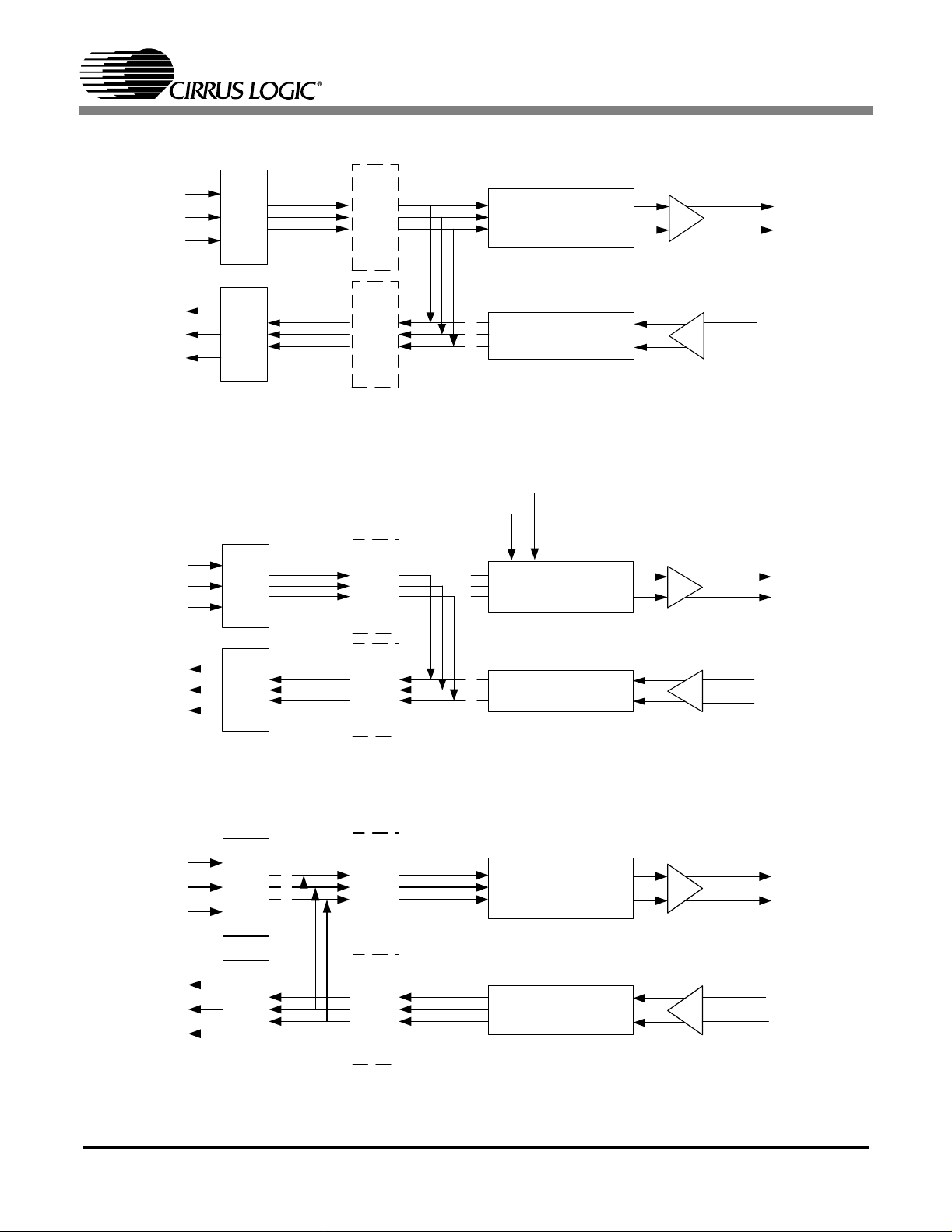
CS61880
TPOS
TNEG
TCLK
RPOS
RNEG
RCLK
MCLK
TAOS
TPOS
TNEG
TCLK
EncoderDecoder
EncoderDecoder
Transmit
Jitter
Attenuator
Jitter
Attenuator
Control &
Pulse Shaper
Clock Recovery &
Data Recovery
Figure 9. Digital Loopback Block Diagram
Transmit
Jitter
Attenuator
Control &
Pulse Shaper
TTIP
TRING
RTIP
RRING
TTIP
TRING
(All One's)
RPOS
RNEG
RCLK
TPOS
TNEG
TCLK
RPOS
RNEG
RCLK
EncoderDecoder
Clock Recovery &
Jitter
Attenuator
Data Recovery
Figure 10. Digital Loopback with TAOS
Transmit
Jitter
Attenuator
Control &
Pulse Shaper
Clock Recovery &
Jitter
Data Recovery
Attenuator
Figure 11. Remote Loopback Block Diagram
RTIP
RRING
TTIP
TRING
RTIP
RRING
DS450PP3 31
Page 32

CS61880
13. HOST MODE
Host mode allows the CS61880 to be configured
and monitored using an internal register set. (Refer
to Table 1, “Operation Mode Selection,” on
page 10). The term, “Host mode” applies to both
Parallel Host and Serial Host modes.
All of the internal registers are available in both Se-
rial and Parallel Host mode; the only difference is
in the functions of the interface pins, which are described in Table 9 on page 32.
Serial port operation is compatible with the serial
ports of most microcontroll er s. Para lle l por t ope ration can be configured to be compatible with 8-bit
microcontrollers from Motorola or Intel, with both
multiplexed or non-multiplexed address/data busses. (Refe r to Table 10 on page 34 for host mode
registers).
13.1 SOFTWARE RESET
A software re s et can be fo rc ed by writin g the Soft-
ware Reset Register (0Ah) (See Sec tion 14.11 on
page 36). A software reset initializes all registers to
their default settings and initializes all internal state
machines.
13.2 Serial Port Operation
Serial port host mode operation is selected when
the MODE pin is left open or set to VCC/2. In this
mode, the CS61880 register set is accessed by setting the chip select (CS) pin low and communicating over the SDI, SDO, and SCLK pins. Timing
over the serial port is independent of the transmit
and receive system timing. Figure 12 illustrates the
format of serial port data transfers.
A read or write is initiated by writing an address/command byte (ACB) to SDI. Only the
ADR0-ADR4 bits are valid; bits ADR5-ADR6 are
do not cares. During a read cycle, the register data
addressed by the ACB is output on SDO on the next
eight SCLK clock cycles. During a write cycle, the
data byte immediately follows the ACB.
Data is written to and read from the serial port in
LSB first format. When writing to the port, SDI
data is sampled by the device on the rising edge of
SCLK. The valid clock edge of the data on SDO is
controlled by the CLKE pin. When CLKE is low,
data on SDO is valid on the falling edge of SCLK.
When CLKE is high, data on SDO is valid on the
raising edge of SCLK. The SDO pin is High-Z
when not transmitting. If the host processor has a
Table 9. Host Control Signal Descriptions
HOST CONTROL SIGNAL DESCRIPTIONS
PIN NAME PIN # HARDWARE SERIAL PARALLEL
MODE 11 LOW VDD/2 HIGH
MUX 43 BITSEN0 - MUX
CODEN
LOOP[7:0], DATA[7:0] 28-21 LOOP[7:0] - DATA[7:0]
32 DS450PP3
/MOT/INTL88CODEN -MOT/INTL
ADDR [4] 12 GND - ADDR[4]
ADDR[3:0] 13 -16 ADDR[3:0] - ADDR [3:0]
INT
SDO/ACK/RDY 83 NC SDO ACK/RDY
SDI/DS
SCLK/AS/ALE 86 G ND SCLK AS/ALE
JASEL/CS
/WR 84 GND SDI DS/WR
R/W/RD 85 GND - R/W/RD
82 Pulled Up INT INT
87 JASEL CS CS
Page 33

CS61880
bidirectional I/O port, SDI and SDO may be tied together.
As illustrated in Figure 12, the ACB consists of a
R/W bit, address field, and two reserved bits. T he
R/W bit specifies if the curr ent regist er access i s a
read (R/W = 1) or a write (R/W = 0) operation. The
address field specifies the register address from
0x00 to 0x1f.
13.3 Parallel Port Operation
Parallel port host mode operation is selected when
the MODE pin is high. In this mode, the CS61880
register set is accessed using an 8-bit, multiplexed
bidirectional address/data bus D[7:0]. Timing over
the parallel port is independent of the transmit and
receive system timing.
The device is compatible with both Intel and Motorola bus formats. The Int el bus for mat is se lected
when the INTL/MOT pin is high and the Motorola
bus format is selected when the INTL/MOT pin is
low. In either mode, the interface can have the address and data multiplexed over the same 8-bit bus
or on separate busses. This operation is controlled
with the MUX pin; MUX = 1 means that the parallel port has its address and data multiplexed over
the same bus; MUX = 0 defines a non-multiplexed
bus. The timing for the different modes are shown
in Figure 28, Figure 26, Figure 25, Figure 27,
Figure 29, Figure 30, Figure 31 and Figure 32.
Multiplexed Intel and Motorola modes are shown
in Figure 28, Figure 26, Figure 25 and Figure 27. A
read or write is initiated by writing an address byte
to D[7:0]. The device latches the address on the
falling edge of ALE(AS). During a read cycle, the
register data is output during the later portion of the
RD or DS pulses. The read cycle is terminated and
the bus returns to a high impedance state as RD
transitions high in Intel timing or DS transitions
high in Motorola timing. During a wr ite c ycle, valid write data must be present and held stable during
the WR or DS pulses.
Non-multiplexed Intel and Motorola modes are
shown in Figure 29, Figure 30, Figure 32 and
Figure 31. The CS pin initiates the cycle, followed
by the DS, RD or WR pin. Data is latched into or
out of the part using the rising edge of the DS, W R
or RD pin. Raising CS ends the cycle.
In Intel mode, the RDY output pin is normally in a
high impedance state; it pulses low once to acknowledge that the chip has been selected, and high
again to acknowledge that data has been written or
read. In Motorola mode, the ACK pin performs a
similar function; it drives high to indicate that the
address has been received by the part, and goes low
again to indicate that data has been written or re ad .
CS
SCLK
SDI
SDO
CLKE=0
DS450PP3 33
R/W
0
000 001D0D1D2D5D3 D6D4 D7
Address/Command Byte Data Input/Output
D0 D1 D2 D5D3 D6D4 D7
Figure 12. Serial Read/Write Format (SPOL = 0)
Page 34

CS61880
13.4 Register Set
The register set available during host mode operations are presented in Table 10. While the upper
three bits of the parallel address are don’t cares on
the CS61880, they should be set to zero for proper
operation.
Table 10. Host Mode Register Set
REGISTERS BITS
ADDR NAM E TYPE 7 6 5 4 3 2 1 0
00h
01h
02h
03h
04h
05h
06h
07h
08h
09h
0Ah
0Bh
0Ch
0Dh
0Eh
0Fh
10h
11h
12h
13h
14h
15h
16h
17h
18h
19h
1Ah
1Bh
1Ch
1Dh
1Eh
1Fh
Revision/IDCODE R IDCODE Refer to Device ID Register (IDR) on page 47
Analog Loopback R/W ALBK 7 ALBK 6 ALBK 5 ALBK 4 ALBK 3 ALBK 2 ALBK 1 ALBK 0
Remote Loopback R/W RLBK 7 RLBK 6 RLBK 5 RLBK 4 RLBK 3 RLBK 2 RLBK 1 RLBK 0
TAOS Enab le R/W TAOE 7 TAOE 6 TAOE 5 TAOE 4 T AOE 3 TAOE 2 TAOE 1 T AOE 0
LOS Status R LOSS 7 LOSS 6 LOSS 5 LOSS 4 LOSS 3 LOSS 2 LOSS 1 LOSS 0
DFM Status R DFMS 7 DFMS 6 DFMS 5 DFMS 4 DFMS 3 DFMS 2 DFMS 1 DFMS 0
LOS Interrupt Enable R/W LOSE 7 LOSE 6 LOSE 5 LOSE 4 LOSE 3 LOSE 2 LOSE 1 LOSE 0
DFM Interrupt Enable R/W DFME 7 DFME 6 DFME 5 DFME 4 DFME 3 DFME 2 DFME 1 DFME 0
LOS Interrupt Statu s R LOSI 7 LOSI 6 LOSI 5 LOSI 4 LOSI 3 LOSI 2 LOSI 1 LOSI 0
DFM Interrupt Status R DFMI 7 DFMI 6 DFMI 5 DFMI 4 DFMI 3 DFMI 2 DFMI 1 DFMI 0
Software Reset R/W SRES 7 SRES 6 SRES 5 SRES 4 SRES 3 SRES 2 SRES 1 SRES 0
Performance Monitor R/W RSVD RSVD RSVD RSVD A3 A2 A1 A0
Digital Loopback R/W DLBK 7 DLBK 6 DLBK 5 DLBK 4 DLBK 3 DLBK 2 DLBK 1 DLBK 0
LOS/AIS Mode Enable R/W LAME 7 LAME 6 LAME 5 LAME 4 LAME 3 LAME 2 LAME 1 LAME 0
Automatic TAOS R/W ATAO 7 ATAO 6 ATAO 5 ATAO 4 ATAO 3 ATAO 2 ATAO 1 ATAO 0
Global Control R/W AI Raisen RSVD Coden FIFO JACF JASEL [1:0]
Line Length Channel ID R/W RSVD RSVD RSVD RSVD RSVD Channel ID
Line Length Data R/W RSVD RSVD RSVD IN_EX LEN[3:0]
Output Disable R/W OENB 7 OENB 6 OENB 5 OENB 4 OENB 3 OENB 2 OENB 1 OENB 0
AIS Stat us R AISS 7 AISS 6 AISS 5 AISS 4 AISS 3 AISS 2 AISS 1 AISS 0
AIS Interrupt Enable R/W AISE 7 AISE 6 AISE 5 AISE 4 AISE 3 AISE 2 AISE 1 AISE 0
AIS Interrupt Status R AISI 7 AISI 6 AISI 5 AISI 4 AISI 3 AISI 2 AISI 1 AISI 0
AWG Broadcast R/W AWGB 7 AWGB 6 AWGB 5 AWGB 4 AWGB 3 AWGB 2 AWGB 1 AWGB 0
AWG Phase Address R/W Channel Address [2:0] Phase Address [4:0]
AWG Phase Data R/W RSVD Sample Data[6:0]
AWG Enable R/W AWGN 7 AWGN 6 AWGN 5 AWGN 4 AWGN 3 A W GN 2 AWGN 1 AWGN 0
RESERVED R/W RSVD 7 RSVD 6 RSVD 5 RSVD 4 RSVD 3 RSVD 2 RSVD 1 RSVD 0
RESERVED R RSVD 7 RSVD 6 RSVD 5 RSVD 4 RSVD 3 RSVD 2 RSVD 1 RSVD 0
RESERVED R/W RSVD 7 RSVD 6 RSVD 5 RSVD 4 RSVD 3 RSVD 2 RSVD 1 RSVD 0
RESERVED R RSVD 7 RSVD 6 RSVD 5 RSVD 4 RSVD 3 RSVD 2 RSVD 1 RSVD 0
BITS Clock Enable R/W BITS 7 BITS 6 BITS 5 BITS 4 BITS 3 BITS 2 BITS 1 BITS 0
RESERVED R/W RSVD 7 RSVD 6 RSVD 5 RSVD 4 RSVD 3 RSVD 2 RSVD 1 RSVD 0
34 DS450PP3
Page 35

CS61880
14. REGISTER DESCRIPTIONS
14.1 Revision/IDcode Register (00h)
BIT NAME Description
[7:4] REVI 7-4 Bits [7:4] are taken from the least-significant nibble of the Device IDCode, which are 0000.
(Refer to Device ID Register (IDR) (See Section 16.3 on page 47).
Bits [3:0] are the revision bits from the JTAG IDCODE register, CS61880 Revision A = 0000.
[3:0] RE VI 3 - 0
14.2 Analog Loopback Register (01h)
BIT NAME Description
[7:0] ALBK 7-0
14.3 Remote Loopback Register (02h)
These bits are subject to change wi th the revi sion of the device (Refer to Device ID Register
(IDR) (See Section 16.3 on page 47).
Enables analog loopbacks. A “1” in bit n enables the loopback for channel n. Refer to Analog
Loopback (See Section 12.2 on page 29) for a complete explanation. Register bits default
to 00h after power-up or reset.
BIT NAME Description
Enables remote loopbacks. A “1” in bit n enables the loopback for channel n. Refer to HOST
[7:0] RLBK 7- 0
14.4
TAOS Enable Register (03h)
BIT NAME Description
[7:0] TAOE 7-0 A “1” in bit n of this register turns on the TAOS generator in channel n. Register bits default
MODE (See Section 13 on page 32) for a complete explanation. Register bi ts default to
00h after power-up or reset.
to 00h after power-up or reset.
14.5 LOS Status Register (04h)
BIT NAME Description
[7:0] LOSS 7-0 Register bit n is read as “1” when LOS is detected on channel n. Register bits default to
00h after power-up or reset.
14.6 DFM Status Register (05h)
BIT NAME Description
[7:0] DFMS 7-0 Driver Failure Monitor. The DFM will set bit n to “1” when it detects a short circuit in channel
n. Register bits de fa ul t to 00h after power-up or res et .
DS450PP3 35
Page 36
14.7 LOS Interrupt Enable Register (06h)
BIT NAME Description
[7:0] LOSE 7-0 Any change in a LOS Status Register will cause the INT
this register is set to “1”. Register bits default to 00h after power-up or reset.
14.8 DFM Interrupt Enable Register (07h)
BIT NAME Description
Enables interrupts for failures detected by the DFM. Any change in a DFM Status Register bit
[7:0] DFME 7-0
14.9
LOS Interrupt Status Register (08h)
BIT NAME Description
[7:0] LOSI 7-0
will cause an interrupt if the corresponding bit is set to “1” in this register. Register bits
default to 00h after po wer-up or reset .
Bit n of this register is set to “1” to indicate a status change in bit n of the LOS Status Register. The bits in this register indicate a change in status since the last cleared LOS interrupt.
Register bits default to 00h after power-up or reset.
CS61880
pin to go low if corresponding bit in
14.10 DFM Interrup t Status Regist er ( 09h)
BIT NAME Description
Bit n of this register is set to “1” to indicate a status change in bit n of the DFM Status Regis-
[7:0] DF MI 7-0
ter. The bits in this register indicate a change in status since the last cleared DFM interrupt.
Register bits default to 00h after power-up or reset.
14.11 Software Reset Register (0Ah)
BIT NAME Description
[7:0] SRES 7-0 Writing to this register initializes all registers to their default settings. Registe r bi t s de fa ul t to
00h after power-up or reset.
14.12 Performance Monitor Register (0Bh)
BIT NAME Description
[7:4] R SVD 7-4 RESERVED (These bits must be set to 0.)
[3:0] A[3:0] The G.772 Monitor is directed to a given channel based on the state of the four least signifi-
cant bits of this register. Register bits defa ul t to 00h a fter power-up or reset . The following table shows the settings needed to select a specific channel’s receiver or transmitter to
perform G.772 monitoring. See Table 6 on page 22 for G.772 Monitor Settings.
14.13 Digital Loopback Reset Register (0Ch)
BIT NAME Description
[7:0] DLBK 7-0 Setting register bit n to “1” enables the digital loopback for channel n. Refer to Digital Loop -
back (See Section 12.3 on page 30) for a complete explanation. Register bits default to
00h after power-up or reset.
36 DS450PP3
Page 37

CS61880
14.14 LOS/AIS Mode Enable Register (0Dh)
BIT NAME Description
[7:0] LAME 7-0 Setting bit n to “1” enables ETSI 300 233 compliant LOS/AIS for channel n; setting bit n to “0”
enables ITU G.775 compliant LOS/AIS for channel n. Regis te r bi ts default to 00h after
power-up or reset.
14.15 Automatic TAOS Register (0Eh)
BIT NAME Description
[7:0] ATAO 7-0 Setting bit n to “1” enables automatic TAOS generation on channel n when LOS is detected.
Register bits default to 00h after power-up or reset.
14.16 Global Control Register (0Fh)
BIT NAME Description
This register is the global control for the AWG Auto-Increment, Automatic AIS insertion,
encoding/decoding and the jitter attenuators location, FIFO length and corner frequency for
all eight channels. Register bits default to 00h after power-up or reset.
The AWG Auto-Increment bit indicates whether to auto-increment the AWG Phase Address
[7] AWG Auto-
Increment
[6] RAISEN
[5] RSVD RESERVED (This bit must be set to 0.)
[4] CODEN
[3] FIFO
LENGTH
[2] JACF
Register (17h) (See Section 14.24 on page 39) after each access. Thus, when this bit is set,
the phase samples address portion of the address register increments after each read or
write access. This bit must be set before any bit in the AWG Enable register is set, if this
function is required.
On LOS, this bit controls the automatic AIS insertion into all eight receiver paths.
0 = Disabl ed
1 = Enabled
Line encoding/decoding Selection
0 = HDB3
1 = AMI
Jitter Attenuator FIFO length Selection
0 = 32 bits
1 = 64 bits
Jitter Attenuator Corner Frequency Selection
0 = 1.25 Hz
1 = 2.50 Hz
These bits select the position of the Jitter Attenuator.
Table 11. Jitter Attenuator Position Selection
[1:0] JASEL [1:0]
DS450PP3 37
JASEL 1 JASEL 0 POSITION
0 0 Disabled
01Transmit Path
1 0 Disabled
1 1 Receive Path
Page 38

14.17 Line Length Channel ID Register (10h)
BIT NAME Description
[7:3] RSVD 7-3 RESERVED (These bits must be set to 0.)
The value written to these bits specify the LIU channel for which the Pulse Shape Configuration Data (register 11h) applies. For example, writing a value of a binary 000 to the 3-LSBs
[2:0] LLID 2-0
will select channel 0. The pulse shape configuration data for the channel specified in this register are written or read through the Line Length Data Register (11h). Regi ster bits default
to 00h after power-up or reset.
14.18 Line Length Data Register (11h)
BIT NAME Description
The value written to the 4-LSBs of this register specifies whether the device is operating in
either E1 75 Ω or E1 120 Ω mode and the associated pulse shape as shown below is being
transmitted. Register bits default to 00h after power-up or reset.
[7:5] RSVD RESERVED (These bits must be set to 0.)
This bit specifies the use of internal (Int_ExtB = 1) or external (Int_ExtB = 0) receiver line
[4] INT_EXTB
[3:0] LEN[3:0]
matching. The line impedance for both the receiver and transmitter are chosen through the
LEN [3:0] bits in this register.
These bits set the line impedance for both the receiver and the transmitter path and the
desired pulse shape for a specific channel. The channel is selected with the Line Length
Channel ID register (0x10). The following table shows the available transmitter pulse
shapes.
CS61880
Table 12. Transmitter Pulse Shape Selection
LEN [3:0] Operation
Mode
0000 E1 120 Ω 3.0 V 12
1000 E1 75 Ω 2.37 V 12
Line Length
Selection
Phase Samples
per UI
14.19 Output Disable Register (12h)
BIT NAME Description
[7:0] OENB 7-0 Set ting bit n of this register to “1” High-Z the TX output driver on channel n of the device.
Register bits default to 00h after power-up or reset.
14.20 AIS Status Register (13h)
BIT NAME Description
[7:0] AISS 7-0 A “1” in bit position n indicates that the receiver has detected an AIS condition on channel n,
which generates an interrupt on the INT
reset.
pin. Register bits default to 00h after power-up or
38 DS450PP3
Page 39

CS61880
14.21 AIS Interrupt Enable Register (14h)
BIT NAME Description
[7:0] AISE 7-0 This register enables changes in the AIS Status register to be reflected in the AIS Interrupt
Status register , thus causing an interrupt on the INT
power-up or reset.
14.22 AIS Interrupt Status Register (15h)
BIT NAME Description
Bit n is set to “1” to indicate a change of status of bit n in the AIS Status Register. The bits in
[7:0] AISI 7-0
this register indicate which channel changed in status since the last cleared AIS interrupt.
Register bits default to 00h after power-up or reset.
14.23 AWG Broadcast Register (16h)
BIT NAME Description
Setting bit n to “1” causes the phase data in the AWG Phase Data Register to be written to
[7:0] AWGB 7-0
the corresponding channel or channels simultaneously. (Refer to Arbitrary Waveform Gen-
erator (See Section 15 on page 42). Regi s te r bi ts defaul t to 00h after power-up or reset .
pin. Register bits default to 00h after
14.24 AWG Phase Address Register (17h)
BIT NAME Description
[7:5] AWGA These bits specify the target channel 0-7. (Refer to Arbitrary Waveform Generator (See
Section 15 on page 42). Regi st er bi ts defa ul t to 00h after po wer-up or reset .
[4:0] PA[4:0] These bits specify 1 of 24 phase sample address locations of the AWG, that the phase data
in the AWG Phase Data Register is written to or read from. Register bits default to 00h
after power-up or reset .
14.25 AWG Phase Data Register (18h)
BIT NAME Description
[7] RSVD RESERVED (This bit must be set to 0.)
These bits are used for the pulse shape data that will be written to or read from th e AWG
phase location specified by the AWG Phase Address Register. The value written to or read
from this register will be written to or read from the AWG phase sample location specified by
[6:0] AWGD [6:0]
the AWG Phase Address register. A software reset through the Software Reset Register
does not effect the contents of this register. The data in each phase is a 7-bit 2’s complement
number (the maximum positive value is 3Fh and the maximum negative value is 40h). (Refer
to Arbitrary Waveform Generator (See Section 15 on page 42). Register bits default to
00h after power-up.
DS450PP3 39
Page 40
14.26 AWG Enable Register (19h)
BIT NAME Description
The AWG enable register is used for selecting the source of the customized transmission
pulse-shape. Setting bit n to “1” in this register selects the AWG as the source of the output
[7:0] AWGN 7-0
pulse shape for channel n. When bit n is set to “0” the pre-programmed pulse shape in the
ROM is selected for transmission on channel n. (Refer to Arbitrary Waveform Generator
(See Section 15 on page 42). Reg ister bits default to 00h after power-up or reset.
CS61880
14.27 Reserved Register
BIT NAME Description
RSVD 7-0 RESERVED
[7:0]
(1Ah)
14.28 Reserved Register (1Bh)
BIT NAME Description
RSVD 7-0 RESERVED
[7:0]
14.29 Reserved Register (1Ch)
BIT NAME Description
[7:0] RSVD 7-0 RESERVED
14.30 Reserved Register (1Dh)
BIT NAME Description
[7:0] RSVD 7-0 RESERVED
14.31 Bits Clock Enable Register (1Eh)
BIT NAME Description
[7:0] BITS 7-0 Writing a “1” to bit n in this register changes channel n to a stand-alone timing recovery unit
used for G.703 clock recovery. (Refer to BUILDI NG INTEGRA T ED TIMING SYSTEMS
(BITS) CLOCK MODE (See Section 8 on page 23) for a better description of the G .703 clock
recovery function). Register bits default to 00h after power-up or reset.
14.32 Reserved Register (1Fh)
BIT NAME Description
[7:0] RSVD 7-0 RESERVED
14.33 Status Registers
The following Status registers are read-only: LOS
Status Register (04h) (See Section 14.5 on
page 35), DFM Status Register (05h) (See Sec-
40 DS450PP3
tion 14.6 on page 35) and AIS Status Register
(13h) (See Section 14.20 on page 38). The
CS61880 generates an interrupt on the INT pin any
time an unmasked status register bit changes.
Page 41

CS61880
14.33.1 Interrupt Enable Registers
The Interrupt Enable registers: LOS Interrupt En-
able Register (06h) (See Section 14.7 on page 36),
DFM Interrupt Enable Register (07h) (See Sec-
tion 14.8 on page 36), AIS Interru pt Ena ble Re g-
ister (14h) (See Section 14.21 on page 39), enable
changes in status register state to cause an interrupt
on the INT pin. Interrupts are maskable on a per
channel basis. When an Interrupt Enable register
bit is 0, the corresponding Status register bit is disabled from causing an interrupt on the INT pin.
NOTE: Disabling an interrupt has no effect on the sta-
tus reflected in the associated status register.
14.33.2 Interrupt Status Registers
The following interrupt status registers: LOS In-
terrupt Status Register (08h) (See Section 14.9
on page 36), DFM Interrupt Status Register
(09h) (See Section 14.10 on page 36), AIS Interrupt Status Register (15h) (See Section 14.22 on
page 39), indicate a change in status of the corresponding status registers in host mode. Reading
these registers clears the interrupt, which deactivates the INT pin.
DS450PP3 41
Page 42
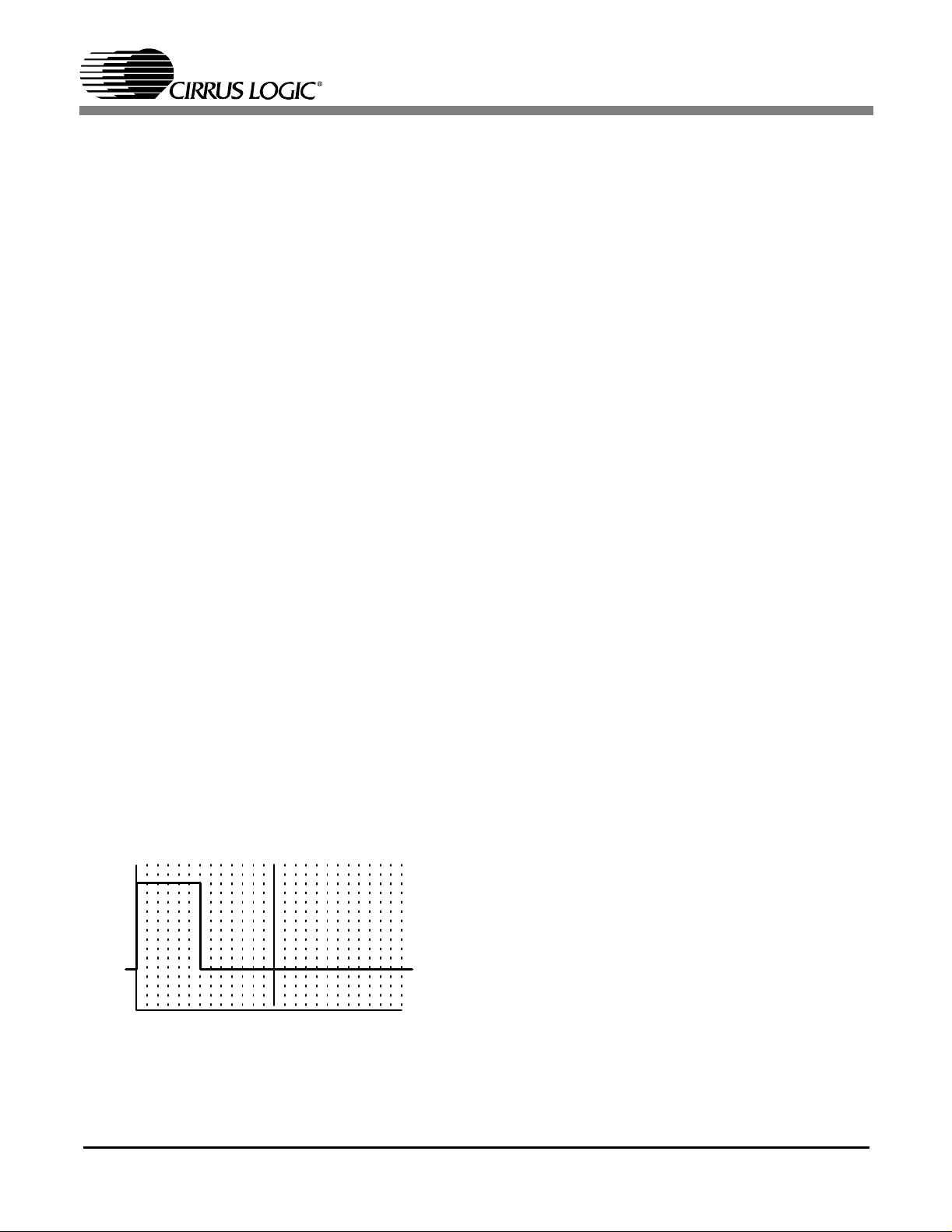
CS61880
15. ARBITRARY WAVEFORM GENERATOR
Using the Arbitrary Waveform Generator (AWG)
allows the user to customize the transmit pulse
shapes to compensate for nonstandard cables,
transformers, protection circuitry, or to reduce
power consumption by reducing the output pulse
amplitude. A channel is configured for a custom
pulse shape by enabling the AWG for that channel
and then storing data representing the pulse shape
into the 24 phase sample locations. Each channel
has a separate AWG, so all eight channels can have
a different customized pulse shape. The microprocessor interface, is used to read fr om or write to the
AWG, while the device is in host mode.
In the AWG RAM, the pulse shape is divided into
two unit intervals (UI). There are 12 phase sample
addresses in each UI. The first UI is for the main
part of the pulse and the second UI is for the “tail”
of the pulse (Refer to Figure 13). A complete pulse-
shape is represented by 24 phase samples. Data
written in the first UI represents a valid pulse
shape, while data in the second UI must be set to
zero at all times. Writing values other that zero to
the second UI will cause the pulse shape to be invalid.
U1 U2
The data in each phase sample is a 7-bit two’s complement number with a maximum positive value of
0x3f, and a maximum negative value of 0x40. The
terms “positive” and “negative” are defined for a
positive going pulse only. The pulse generation circuitry automatically inverts the pulse for negative
going pulses. The data stored in the lowest phase
address corresponds to the first phase sample that
will be transmitted in time. The typical voltage step
for each mode of operation is as follows: for E1
75 Ω mode the typical voltage step is 42 mV/LSB
and for E1 120 Ω mode the typical voltage step is
54 mV/LSB all voltage steps are measured across
the transformer secondary.
The following procedure describes how to enable
and write data into the AWG RAM to produce customized pulse shapes to be tr ansmitted for a specific channel or channels. First, enable the AWG
function for a specific channel or channels by writing a “1” to the corresponding bits in the AWG En-
able Register (19h) (See Section 14.26 on
page 40). When the corresponding bit or bits in the
AWG Enable Register are set to “0” pre-programmed pulse shapes are selected for transmission. Then the desired channel and phase sample
address must be written to the AWG Phase Ad-
dress Register (17h) (See Section 14.24 on
page 39). Once the c hannel and phase sample address have been written, the actual phase sample
data may be entered into the AWG Phase Data
Register (18h) (See Section 14.25 on page 39) at
the selected phase sample address sel ected by the
lower five bits of the AWG Phase Address Regis-
ter (17h) (See Section 14.24 on page 39)).
To change the phase sample address of the selected
channel the user may use either of the following
steps. The user can re-write the phase sampl e ad-
E1 AWG Example
dress to the AWG Phase Address Register or set the
Auto-Increment bit (Bit 7) in the Global Control
Register (0Fh) (See Section 14.16 on page 37) to
Figure 13. Arbitrary Waveform UI
42 DS450PP3
“1” before writing to the AWG Phas e Data Regi ster. When this bit is set to “1” only the first phase
Page 43

CS61880
sample address (00000 binary) needs to be written
to the AWG Phase Address Register (17h) (See
Section 14.24 on page 39), and each subsequent access (read or write) to the AWG Phase Data Reg-
ister (18h) (See Section 14.25 on page 39) will
automatically increment the phase sample address.
The channel address, however, remains unaffected
by the Auto-Increment mode. The AWG Phase
Address Register (17h) (See Section 14.24 on
page 39) needs to be re-written in order to re-start
the phase sample address sequence from the new
phase sample address.
The AWG Broadcast function allows the same data
to be written to multiple channels simultaneously.
This is done with the use of the AWG Broadcast
Register (16h) (See Section 14.23 on page 39),
each bit in the AWG Broadcast Register corresponds to a different channel ( e.g. bit 0 is channel
0, and bit 3 is channel 3 and etc.). To use the AWG
Broadcast function MCLK must be present. When
MCLK is inactive the AWG Broadcast function is
disabled.
To write the same pulse shaping data to multiple
channels, simple set the corresponding bit to “1” in
the AWG Broadcast Register (16h) (See Section
14.23 on page 39) before accessing the AWG
phase data register. This function only requires that
one of the eight c hanne l addresses be written to the
AWG Phase Address Register (17h) (See Section
14.24 on page 39). During an AWG read sequence,
the bits in the AWG Broadcast Register are ignored. During an AWG write sequence, the selected channel or channels are specified by both the
channel address specified by the upper bits of the
AWG Phase Address Register (17h) (See Section
14.24 on page 39) and the selected channel or chan-
nels in the AWG Broadcast Register (16h) (See
Section 14.23 on page 39).
During a multiple channel write the first channel
that is written to, is the channel that was addressed
by the AWG Phase Address Register. Thi s channel’s bit in the AWG Broadcast Register can be set
to either “1” or “0”.
For a more descriptive explanation of how to use
the AWG function refer to the Application Note
AN204, How To Use The CS61880/CS61884 Arbitrary Waveform Generator.
16. JTAG SUPPORT
The CS61880 supports the IEEE Boundary Scan
Specification as described in the IEEE 1149.1 standards. A Test Access Port (TAP) is provided that
consists of the TAP controller, the instruction register (IR), by-pass register (BPR), device ID register (IDR), the boundary scan register (BSR), and
the 5 standard pins (TRST, TCK, TMS, TD I, and
TDO). A block diagram of the test access por t is
shown in Figure 14 on page 44. The test clock input (TCK) is used to sample input data on TDI, and
shift output data through TDO. The TMS input is
used to step the TAP controller through its various
states.
The instruction regist er is used to select tes t e xec ution or register access. The by-pass register provides a direct connection between the TDI input
and the TDO output. The device identification register contains a 32-bit device identifier.
The Boundary Scan Register is used to support testing of IC inter-connectivity. Using the Boundary
Scan Register, the digital input pins can be sampled
and shifted out on TDO. In addition, this register
can also be used to drive digital output pins to a
user defined state.
DS450PP3 43
Page 44

CS61880
TDI
TCK
TMS
Digital output pins
Digital input pins
parallel latched
output
Boundary Scan Data Register
Device ID Data Register
Bypass Data Register
Instructio n (shift) Register
parallel latched output
TAP
Controller
Figure 14. Test Access Port Architecture
JTAG BLOCK
MUX TDO
16.1 TAP Controller
The TAP Controller is a 16 state synchronous state
machine clocked by the rising edge of T CK. The
TMS input governs state transitions as shown in
Figure 15. The value shown next to each state tran-
sition in the diagram is the value that must be on
TMS when it is sampled by the rising edge of TCK.
16.1.1 JTAG Reset
TRST resets all JTAG circuitry.
16.1.2 Test-Logic-Reset
The test-logic-rese t state is us ed to disable t he test
logic when the part is in normal mode of operation.
This state is entered by asynchronously asserting
TRST or forcing TMS High for 5 TCK periods.
16.1.3 Run-Test-Idle
The run-test-idle state is used to run tests.
16.1.4 Select-DR-Scan
This is a temporary controller state.
16.1.5 Capture-DR
In this state, the Boundary Scan R egister captures
input pin data if the current instruction is EXTEST
or SAMPLE/PRELOAD.
16.1.6 Shift-DR
In this controller state, the active test data register
connected between TDI and TDO, as determi ned
by the current instruction, shifts data out on TDO
on each rising edge of TCK.
16.1.7 Exit1-DR
This is a tem porary state. Th e test data r egist er selected by the current instruction r etains it s previous
value.
44 DS450PP3
Page 45

CS61880
1
0
Test-Logic-Reset
0
Run-Test/Idle
11
Figure 15. TAP Controller State Diagr am
Select-DR-Scan
0
1
Capture-DR
0
Shift-DR
1
Exit1-DR
0
Pause-DR
1
0
Exit2-DR
11
Update-DR
11
00
0
1
0
Select-IR-Scan
1
Capture- IR
Shift- IR
Exit1-IR
Pause- IR
0
Exit2- IR
Update-I R
1
0
0
0
1
1
0
0
1
16.1.8 Pause-DR
The pause state allows the tes t controlle r to temporarily halt the shifting of data through the current
test data register.
16.1.9 Exit2-DR
This is a tem porary state. Th e test data r egist er selected by the current instruction r etains it s previous
value.
16.1.10 Update-DR
The Boundary Scan Register is provided with a
latched parallel output to prevent changes while
data is shifted in response to the EXTEST and
SAMPLE/PRELOAD instructions. When the TAP
controller is in this state and the Boundary Scan
Register is selected, data is latched into the parallel
output of this register from the shift-register path
on the falling edge of TCK. The data held at the
latched parallel output changes only in this state.
16.1.11 Select-IR-Scan
This is a temporary controller state. The test data
register select ed by the current instruction reta ins
its previous state.
16.1.12 Capture-IR
In this controller state, the instruction register is
loaded with a fixed value of “01” on the rising edge
of TCK. This supports fault-isolation of the boardlevel serial test data path.
16.1.13 Shift-IR
In this state, the shift register contained in the instruction register is connected between TDI and
TDO and shifts data one stage towards its serial
output on each rising edge of TCK.
DS450PP3 45
Page 46
16.1.14 Exit1-IR
CS61880
This is a tem porary state. Th e test data r egist er selected by the current instruction r etains it s previous
value.
16.1.15 Pause-IR
The pause state allows the tes t controlle r to temporarily halt the shifting of data through the instruction register.
16.1.16 Exit2-IR
This is a tem porary state. Th e test data r egist er selected by the current instruction r etains it s previous
value.
16.1.17 Update-IR
The instruction shifted into the instruction register
is latched into the parallel output from the shift-register path on the falling edge of TCK. When the
new instruction has been latched, it becomes the
current instruction. T he test data register s sele cted
by the current instruction retain their previous value.
16.2 Instruction Register (IR)
The 3-bit Instruction register selects the test to be
performed and/or the data register to be acces sed.
The valid instructions are shifted in LSB first and
are listed in Table 13:
Tab l e 13. JTA G Ins tr u ctio n s
IR CODE INSTRUCTION
000 EXTEST
100 SAMPLE/PRELOAD
110 IDCODE
111 BYPASS
16.2.1 EXTEST
The EXTEST instruction allows t esting of off -chip
circuitry and board-level interconnect. EXTEST
connects the BSR to the TDI and TDO pins.
16.2.2 SAMPLE/PRELOAD
The SAMPLE/PRELOAD instruction samples all
device inputs and outputs. This instruction places
the BSR between the TDI and TDO pins. The BSR
is loaded with samples of the I/O pins by the Capture-DR state.
16.2.3 IDCODE
The IDCODE instruction connects the device identification register to the TDO pin. The device identification code can then be shifted out TDO using
the Shift-DR state.
16.2.4 BYPASS
The BYPASS instruction connects a one TCK delay register between TDI and TDO. The instruction
is used to bypass the device.
46 DS450PP3
Page 47
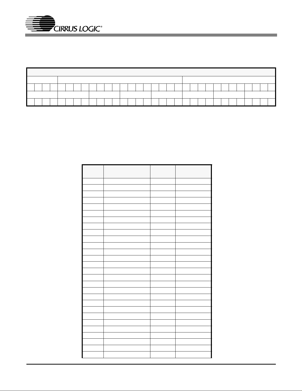
CS61880
16.3 Device ID Register (IDR)
Revision section: 0h = Rev A, 1h = Rev B and so on. The device I dentification Code [27 - 12] is derived
from the last three digits of the part number (880). The LSB is a constant 1, as defined by IEEE 1149.1.
CS61880 IDCODE REGISTER(IDR)
REVISION DEVICE IDCODE REGISTER MANUF ACTURER CODE
31 30 29 28 27 26 25 24 23 22 21 20 19 18 17 16 15 14 13 12 11 10 9 8 7 6 5 4 3 2 1 0
0h 0h 8h 8h 0h 0h Ch 9h
00000000100010000000000011001001
17. BOUNDARY SCAN REGISTER (BSR)
The BSR is a shift register that provides access to the digital I/O pins. The BSR is used to read and write
the device pins to verify interchip connectivity. Each pin has a corresponding scan cell in the register. The
pin to scan cell mapping is given in the Boundary Scan Register description shown in Table 14.
NOTE: Data is sh ifted LSB fir s t i n t o th e BSR re giste r .
Table 14. Boundary Scan Register
BSR
Bit
0 LOS7 O LOS7
1 RNEG7 O RNEG7
2 RPOS7 O RPOS7
3 RCLK7 O RCLK7
4 - Note 2 HIZ7_B
5 TNEG7 I TNEG7
6 TPOS7 I TPOS7
7 TCLK7 I TCLK7
8 LOS6 O LOS6_B
9 RNEG6 O RNEG6
10 RPOS6 O RPOS6
11 RCLK6 O RCLK6
12 - Note 2 HIZ6_B
13 TNEG6 I TNEG6
14 TPOS6 I TPOS6
15 TCLK6 I TCLK6
16 MCLK I MCLK
17 MODE I MODE_TRI
18 MODE I MODE_IN
19 ADDR4 I ADDR4
20 ADDR3 I ADDR3
21 ADDR2 I ADDR2
22 ADDR1 I ADDR1
23 ADDR0 I ADDR0
24 LOOP0/D0 I LPT0
25 LOOP0/D0 I LPI0
26 LOOP0/D0 O LPO0
27 LOOP1/D1 I LPT1
Pin
Name
Cell
Ty pe
Bit
Symbol
DS450PP3 47
Page 48

Table 14. Boundary Scan Register (Continued)
CS61880
BSR
Bit
28 LOOP1/D1 I LPI1
29 LOOP1/D1 O LPO1
30 LOOP2/D2 I LPT2
31 LOOP2/D2 I LPI2
32 LOOP2/D2 O LPO2
33 LOOP3/D3 I LPT3
34 LOOP3/D3 I LPI3
35 LOOP3/D3 O LPO3
36 LOOP4/D4 I LPT4
37 LOOP4/D4 I LPI4
38 LOOP4/D4 O LPO4
39 LOOP5/D5 I LPT5
40 LOOP5/D5 I LPI5
41 LOOP5/D5 O LPO5
42 LOOP6/D6 I LPT6
43 LOOP6/D6 I LPI6
44 LOOP6/D6 O LPO6
45 LOOP7/D7 I LPT7
46 LOOP7/D7 I LPI7
47 LOOP7/D7 O LPO7
48 - Note 1 LPOEN
49 TCLK1 I TCLK1
50 TPOS1 I TPOS1
51 TNEG1 I TNEG1
52 RCLK1 O RCLK1
53 RPOS1 O RPOS1
54 RNEG1 O RNEG1
55 - Note 2 HIZ1_B
56 LOS1 O LOS1
57 TCLK0 I TCLK0
58 TPOS0 I TPOS0
59 TNEG0 I TNEG0
60 RCLK0 O RCLK0
61 RPOS0 O RPOS0
62 RNEG0 O RNEG0
63 - Note 2 HIZ0_B
64 LOS0 O LOS0
65 MUX I MUX
66 LOS3 O LOS3
67 RNEG3 O RNEG3
68 RPOS3 O RPOS3
69 RCLK3 O RCLK3
70 - Note 2 HIZ3_B
71 TNEG3 I TNEG3
72 TPOS3 I TPOS3
Pin
Name
Cell
Ty pe
Bit
Symbol
48 DS450PP3
Page 49

Table 14. Boundary Scan Register (Continued)
CS61880
BSR
Bit
73 TCLK3 I TCLK3
74 LOS2 O LOS2
75 RNEG2 O RNEG2
76 RPOS2 O RPOS2
77 RCLK2 O RCLK2
78 - Note 2 HIZ2_B
79 TNEG2 I TNEG2
80 TPOS2 I TPOS2
81 TCLK2 I TCLK2
82 INT_B O INT_B
83 RDY O RDYOUT
84 - Note 3 RDYOEN
85 WR_B I WR_B
86 RD_B I RD_B
87 ALE I ALE
88 CS_B I CS_B
89 CS_B I CS_B_TRI
90 INTL I INTL
91 CBLSEL I CBLSEL_TRI
92 CBLSEL I CBLSEL_IN
93 TCLK5 I TCLK5
94 TPOS5 I TPOS5
95 TNEG5 I TNEG5
96 RCLK5 O RCLK5
97 RPOS5 O RPOS5
98 RNEG5 O RNEG5
99 - Note 2 HIZ5_B
100 LOS5 O LOS5
101 TCLK4 I TCLK4
102 TPOS4 I TPOS4
103 TNEG4 I TNEG4
104 RCLK4 O RCLK4
105 RPOS4 O RPOS4
106 RNEG4 O RNEG4
107 - Note 2 HIZ4_B
108 LOS4 O LOS4
109 TXOE I TXOE
110 CLKE I CLKE
Pin
Name
Cell
Ty pe
Bit
Symbol
Notes:
1) LPOEN controls the LOOP[7:0] pins. Setting LPOEN to “1” configures LOOP[7:0] as outputs. The o utput value driven
on the pins are determined by the values written to LPO[7:0]. Setting LPOEN to “0” High-Z all the pins. In this mode,
the input values driven to these LOOP[7:0] can be read via LPI [7:0].
2) HIZ_B controls the RPOSx, RNEGx, and RCLKx pins. When HIZ_B is High, the outputs are enabled; when HIZ_B is
Low, the out puts are placed in a high impedance state (High-Z).
3) RD YOEN controls the ACK_B pin. Setting RDYOEN to “1” enables output on ACK_B. Setting ACKEN to “0” High -Z
the ACK_B pin.
DS450PP3 49
Page 50

18. APPLICATIONS
0.1
Note 1
+3.3V
µ
F
0.1
Note 1
CS61880
+
+
µ
F
68µF
Note 2
0.1
GNDIO
75
Cable
NC
120
Cable
Ω
Ω
RGND
+3.3V
µ
F
+3.3V
TGND
RV+
VCCIO
+
TV+
RTIP
RRING
0.1
µ
F
R1
RECEIVE
LINE
R2
T1 1:2
CS61880
One Channel
TRING
TRANSMIT
LINE
TTIP
T2 1:1.15
13.3k
Ω
CBLSEL
REF
GND
Component E1 75Ω Coaxial Cable E1 120Ω Twisted Pair Cable
R1 (Ω) 15 15
R2 (Ω) 15 15
Notes:1) Required Capacitor between each TV+, RV+, VCCIO and TGND, RGND, GNDIO respec-
tively.
2) Common decoupling capacitor for all TVCC and TGND pins.
Figure 16. Internal RX/TX Impedance Matching
50 DS450PP3
Page 51

GNDIO
Ω
120
Cable
NC
0.1
RGND
+3.3V
µ
F
CS61880
+3.3V
+
0.1µF
Note 1
RV+
VCCIO
0.1µF
Note 1
TV+
RTIP
+
+
RRING
CS61880
TRING
One Channel
TTIP
CBLSEL
TGND
1k
Ω
0.1µF
1k
Ω
13.3k
68µF
Note 2
R1
RECEIVE
LINE
R2
T1 1:2
TRANSMIT
LINE
T2 1:1.15
Ω
75
Ω
Cable
GND
Component E1 75 Ω Coaxial Cable E1 120 Ω Twisted Pair Cab le
R1 (Ω) 9.31 15
R2 (Ω) 9.31 15
Notes: 1)Required Capacitor betwe en each TV+, RV+, VCCIO and TGND, RGND, GNDIO
REF
GND
respectively.
2)Common decoupling capacitor for all TVCC and TGND pins.
Figure 17. Internal TX, Extern a l RX Impedan ce Matching
DS450PP3 51
Page 52

CS61880
18.1 Transformer Specifications
Recommended transformer specifications are
shown in Table 15. Any transformer used with the
CS61880 should meet or exceed these specifications.
Table 15. Transformer Specifications
Descriptions Specifications
Turns Ratio Receive 1:2
Turns Ratio Transmit 1:1.15
Primary Inductance 1. 5 mH min @ 1024 kHz
Primary Leakage Inductance
Secondary leakage Inductance
Inter winding Capacitance 18 pF max , primary to
ET-Constant 16 V - µs min
0.3 µH max @ 1024 kHz
0.4 µH max @ 1024 kHz
secondary
18.2 Crystal Oscillator Specifications
When a reference clock signal is not available, a
CMOS crystal oscillator may be used as the reference clock signal. The oscillator must have a minimum symmetry of 40-60% and minimum stability
of + 100 ppm.
18.3 Line Protection
Secondary protection components can be added to
the line interface circuitry to provide lightning
surge and AC power-cross immunity. For additional information on the different electrical safety
standards and speci fic applications circuit recommendations, refer to Application Note AN034, Sec-
ondary Line Protection for T1 and E1 Cards.
52 DS450PP3
Page 53

CS61880
19. CHARACTERISTICS AND SPECIFICATIONS
19.1 Absolute Maximum Ratings
CAUTION: Operations at or beyond these limits may result in permanent damage to the device. Normal operation
is not guaranteed at these extremes.
Parameter Symbol Min. Max Units
DC Supply
(referenced to RGND = TGND = 0V)
DC Supply VCCIO -0.5 4.6 V
Input Voltage, Any Digital Pin except CBLSEL, MODE and
LOOP(n) pins (referenced to GNDIO = 0V)
Input Voltage CBLSEL, MODE & LOOP(n) Pins
(referenced to GNDIO = 0V)
Input voltage, RTIP and RRING Pins TGND -0.5 TV+ +0.5 V
ESD voltage, Any pin Note 1 2k - V
Input current, Any Pin Note 2 I
Maximum Power Dissipation, In package P
Ambient Operating Temperature T
Storage Temperature T
RV+
TV+
V
IH
V
IH
IH
p
A
stg
-
-
4.0
4.0
V
V
GNDIO -0.5 5.3 V
GNDIO -0.5 VCCIO +0.5 V
-10 +10 mA
-1.73W
-40 85 C
-65 150 C
19.2 Recommended Operating Conditions
Parameter Symbol Min. Typ Max Units
DC Supply RV+, TV+ 3.135 3.3 3.465 V
DC Supply VCCIO 3.135 3. 3 3.465 V
Ambient operating Temperature T
Power Consumption, E1 Mode, 75 Ω line load Notes 3, 4, 5
Power Consumption, E1 Mode, 120 Ω line load Notes 3, 4, 5
Notes: 1. Human Body Model
2. Transient current of up to 100 mA will not cause SCR latch-up. Also TTIP, TRING, TV+ and TGND can
withstand a continuous current of 100 mA.
3. Power consumption while driving line load over the full operating temperature and power supply voltage
range. Includes all IC channels and loads. Digital inputs are within 10% of the supply rails and digital
outputs are driving a 50 pF capacitive load.
4. Typical consumption corresponds to 50% ones density for at 3.3 V.
5. Maximum consumption corresponds to 100% ones density at 3.465 V.
6. This specification guarantees TTL compatibility (V
= 2.4 V @ I
OH
7. Output drivers are TTL compatible.
8. Pulse amplitude measured at the output of the transformer across a 75 Ω load.
9. Pulse amplitude measured at the output of the transformer across a 120 Ω load.
A
-
-
-40 25 85 C
- 660 1040 mW
- 640 950 mW
= -400 µA).
OUT
DS450PP3 53
Page 54

19.3 Digital Characteristics
(TA = -40° C to 85° C; TV+, RV+ = 3.3 V ±5%; GND = 0 V)
Parameter Symbol Min. Typ Max Units
CS61880
High-Level Input Voltage Note 6 V
Low-Level Input Voltage Note 6 V
LOOP[7:0] Low-Level Input Voltage V
LOOP[7:0] Mid-Level Input Voltage V
LOOP[7:0] High-Level Input Voltage V
High-Level Output Voltage Notes 6, 7
I
= -400 µA
OUT
Low-Level Output Voltage Notes 6, 7
I
= 1.6 mA
OUT
V
V
IH
IL
IHL
IHM
IHH
OH
OL
2.0 - - V
--0.8V
- - 1/3 VCCIO-0.2 V
1/3 VCCIO +0.2 1/2 VCCIO 2/3 VCCIO-0.2 V
2/3 VCCIO +0.2 - - V
2.4 - - V
--0.4V
Input Leakage Current -10 - +10 µA
Input leakage for LOOP pins -150 +150 µA
19.4 Transmitter Analog Characteristics
(TA = -40° C to 85° C; TV+, RV+ = 3.3 V ±5%; GND = 0 V)
Parameter Min. Typ Max Units
Output Pulse Amplitudes E1 75 Ω
Notes 8, 9, 11 E1 120 Ω
Ratio of Positive to Negative pulses
Notes 8, 9, 11 Amplitude at center of pulse interval
Width at 50% of nominal amplitude
Pulse Amplitude of a space E1 120 Ω
E1 75 Ω
Transmit Return Loss 51 kHz to 102 kHz
102 kH to 2048 kHz
Notes 10, 11, 12 2048 kHz to 3072 kHz
Jitter Added by the Transmitter 10 Hz - 8 kHz
8kHz - 40kHz
Notes 10, 13 10 Hz - 40 kHz
Broad Band
Transmitter Short Circuit Current per channel - - 50 mA RMS
2.14
2.7
0.95
0.95
-0.3
-0.237
-14
-14
-14
-
-
-
-
2.37
3.0
-
-
-
-
-20
-19
-18
0.010
0.009
0.007
0.015
2.6
3.3
1.05
1.05
0.3
0.237
-
-
-
0.020
0.025
0.025
0.050
V
V
V
V
dB
UI
54 DS450PP3
Page 55

CS61880
19.5 Receiver Analog Characteristics
(TA = -40° C to 85° C; TV+, RV+ = 3.3 V ±5%; GND = 0 V))
Parameter Min. Typ Max Units
Allowable Cable Attenuation @ 1024 kHz - - - 12 dB
RTIP/RRING Input Impedance E1 120 Ω Load
(Internal Line matching mode) E1 75 Ω Load
Note 10
RTIP/RRING Input Impedance E1 120 Ω Load
(External Line matching mode) E1 75 Ω Load
Note 10
Receiver Dynamic Range 0.5 - - Vp
Signal to Noise margin (Per G.703, O151 @ 6 dB cable Atten). - -18 - dB
Receiver Squelch Level 150 mV
LOS Threshold - 200 - mV
LOS Hysteresis 50 mV
Data Decision Threshold
Note 10
Input Jitter Tolerance 1 Hz - 1.8 Hz
Notes 10, 14, 16 2 0 Hz - 2.4 kHz
18 kHz - 100 kHz
Input Return Loss 51 kHz - 102 kHz
102 kHz - 2048 kHz
Notes 10, 11, 12 2048 kHz - 3072 kHz
-
-
-
-
41 50 59 % of
18
1.5
0.2
-18
-18
-18
13k
50
13k
13k
-
-
-
-28
-30
-27
-
-
-
-
peak
-
-
-
-
-
-
UI
dB
Ω
Ω
Notes: 10. Parameters guaranteed by design and characterization.
11. Using components on the CDB61880 evaluation board in Internal Match Impedance Mode.
12. Return loss = 20log10 ABS((Z1 + Z0) / (Z1 - Z0)) where Z1 - impedance of the transmitter or receiver,
and Z0 = cable impedance.
13. Assuming that jitter free clock is input to TCLK.
14. Jitter t olerance for 6 dB input signal levels. Jitter tolerance increases at lower frequencies. HDB3 coders
enabled.
15. In Data Recovery Mode.
16. Jitter Attenuator in the receive path.
DS450PP3 55
Page 56

19.6 Jitter Attenuator Characteristics
(TA = -40° C to 85° C; TV+, RV+ = 3.3 V ±5%; GND = 0 V)
Parameter Min. Typ Max Units
CS61880
Jitter Attenuator Corner Frequency
Note 10, 18
-
-
1.25
2.50
-
Hz
-
(Depends on JACF Bit in host mode)
E1 Jitter Attenuation 3 Hz to 40 Hz
Note 10, 17 400 Hz to 100 kHz
Attenuator Input Jitter Tolerance before FIFO 32-bit FIFO
over flow and under flow Note 10 64-bit FIFO
Delay through Jitter Attenuator Only 32-bit FIFO
Note 10 64-bit FIFO
+ 0.5
-19.5
-
-
-
-
24
56
16
32
-
-
-
dB
-
-
-
-
-
UI
UI
UI
UI
Intrinsic Jitter in Remote Loopback Notes 10, 16 --0.11UI
Notes: 17. Attenuation measured with sinusoidal input filter equal to 3/4 of measured jitter tolerance. Circuit
attenuates jitter at 20 dB/decade above the corner frequency. Output jitter can increase significantly
when more than 28 UI’s are input to the attenuator.
18. Measurement is not effected by the position of the Jitter Attenuator.
+ 10
+ 0.5
0
- 6
- 10
ITU G.736
1.4K20 40040
1K 10K
100K
Attenuation in dB
- 19.5
- 20
- 30
- 40
- 50
- 60
- 70
2
110
TYP. E1 @ 2.5 Hz CF
TYP. E1 @ 1.25 Hz CF
100
57
Frequency in Hz
Figure 18. Jitter Transfer Characteristic vs. G.736 & TBR 12/13
56 DS450PP3
Page 57

1000
CS61880
300
TYP. E1 Performan ce
138
100
28
18
10
1.5
1
PEAK TO PEAK JITTER (UI)
.4
.2
.1
110 1k100 100k1.8 4.9 20 300 10k2.4k 18k
ITU G.823
FREQUENCY IN Hz
Figure 19. Jitter Tolerance Characteristic vs. G.823
DS450PP3 57
Page 58
CS61880
19.7 Master Clock Switching Characteristics
Parameter Symbol Min. Typ Max Units
MASTER CLOCK (MCL K )
Master Clock Frequency MCLK 2.048 M H z
Master Clock Tolerance - -100 +100 ppm
Master Clock Duty Cycle - 40 50 60 %
19.8 Transmit Switching Characteristics
Parameter Symbol Min. Typ Max Units
TCLK Frequency 1/t
pw2
TPOS/TNEG Pulse Width (RZ Mode) 236 244 252 ns
TCLK T o l erance (NRZ Mode) -50 - 50 PPM
TCLK Duty Cycle t
pwh2/tpw2
TCLK Pulse Width 20 - - ns
TCLK Burst Rate Note 10 --20MHz
TPOS/TNEG to TCLK Falling Setup Time (NRZ Mode) t
TCLK Falling to TPOS/TNEG Hold time (NRZ Mode) t
su2
h2
TXOE Asserted Low to TX Driver HIGH-Z - - 1 µs
TCLK Held Low to Driver HIGH-Z Note 20 81220µs
- 2.048 - MHz
--90%
25 - - ns
25 - - ns
19.9 Receive Switching Characteristics
Parameter Symbol Min. Typ Max Units
RCLK Duty Cycle Note 10 40 50 60 %
RCLK Pulse Width Note 10 196 244 328 ns
RPOS/RNEG Pulse Width (RZ Mode) Note 10 200 244 300 ns
RPOS/RNEG to RCLK rising setup time Note 10 t
RPOS/RNEG to RCLK hold time Note 10 t
su
h
RPOS/RNEG Output to RCLK Output (RZ Mode) Note 10 - - 10 ns
Rise/Fall Time, RPOS, RNEG, RCLK, LOS outputs Note 19 t
, t
r
f
Notes: 19. Output load capacitance = 50 pF.
20. MCLK is not active.
200 244 ns
200 244 ns
- - 85 ns
58 DS450PP3
Page 59

RCLK
CS61880
RPOS/RNEG
CLKE = 1
RPOS/RNEG
CLKE = 0
Figure 20. Recovered Clock and Data Switching Characteristics
TCLK
t
su
t
pwh2
t
pw2
t
h
t
su
t
h
TPOS/TNEG
Figure 21. Transmit Clo ck an d Data Switc h ing Characteristics
Any Digital Output
t
su2
t
r
90%
t
90%
10%
Figure 22. Signal Rise and Fall Characteristics
h2
t
10%
f
DS450PP3 59
Page 60
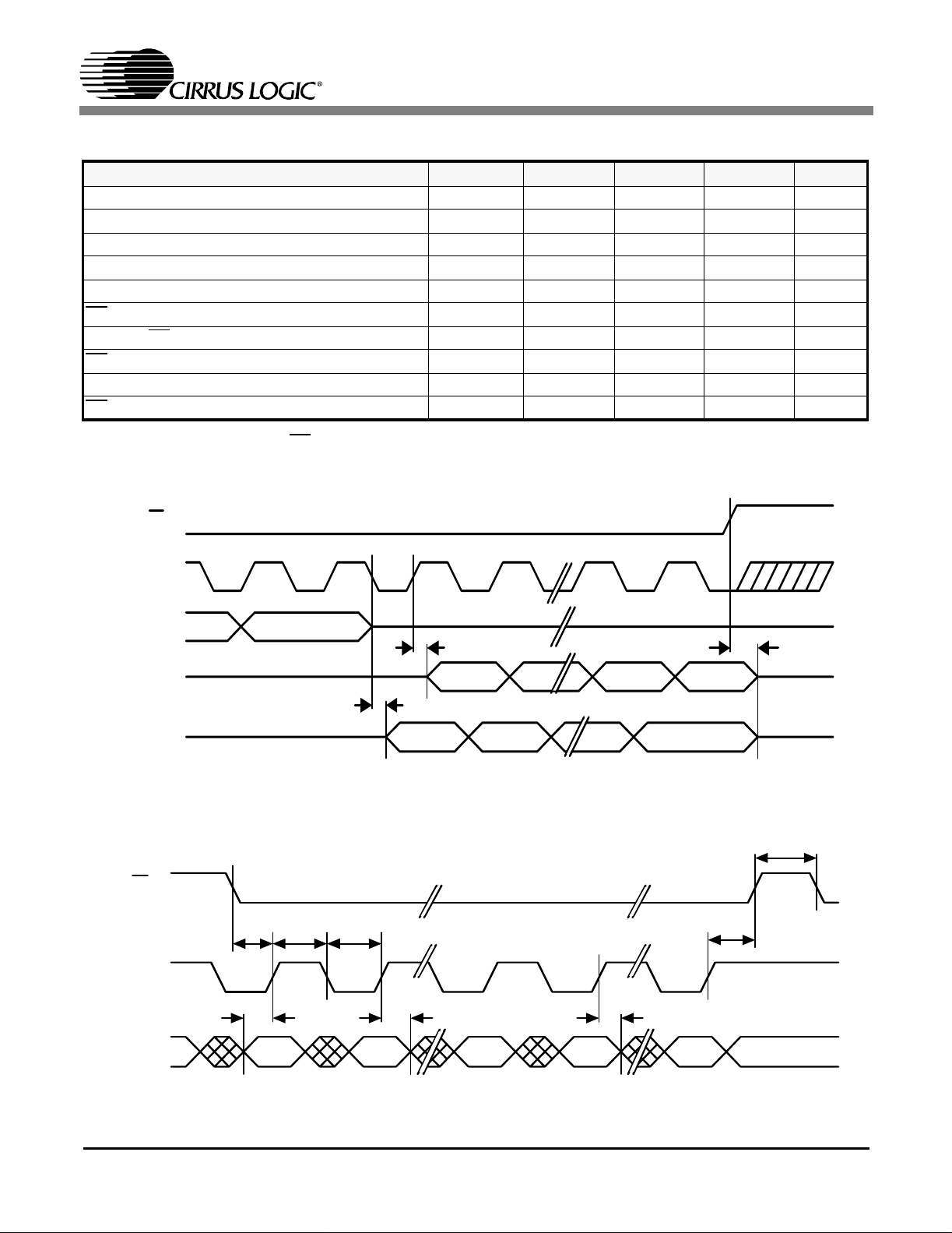
CS61880
19.10 Switching Characteristics - Serial Port
Parameter Symbol Min. Typ. Max Unit
SDI to SCLK Setup Time t
SCLK to SDI Hold Time t
SCLK Low Tim e t
SCLK High Time t
SCLK Rise and Fall Time t
to SCLK Setup Time t
CS
SCLK to CS
Inactive Time t
CS
Hold Time Note 21 t
SDO Valid to SCLK Note 21 t
to SDO High Z t
CS
dc
cdh
cl
ch
, t
r
cc
cch
cwh
cdv
cdz
f
Notes: 21. If SPOL = 0, then CS should return high no sooner than 20 ns after the 16th rising edge of SCLK during
a serial port read.
CS
-20-ns
-20-ns
-50-ns
-50-ns
-15-ns
-20-ns
-20-ns
-70-ns
-60-ns
-50-ns
SCLK
SDO
CLKE=0
SDO
CLKE=1
CS
SCLK
SDI
LAST ADDR BIT
t
t
cdv
cdv
D0
D0 D1
D1 D6 D7
D6
D7
t
cdz
HIGH Z
Figure 23. Serial P o rt Read Timing Diagram
t
cwh
t
t
cc
ch
t
dc
t
cl
t
cdh
t
cdh
t
cch
SDI
LSB LSB MSB
Figure 24. Serial Port Write Timing Diagram
60 DS450PP3
Page 61
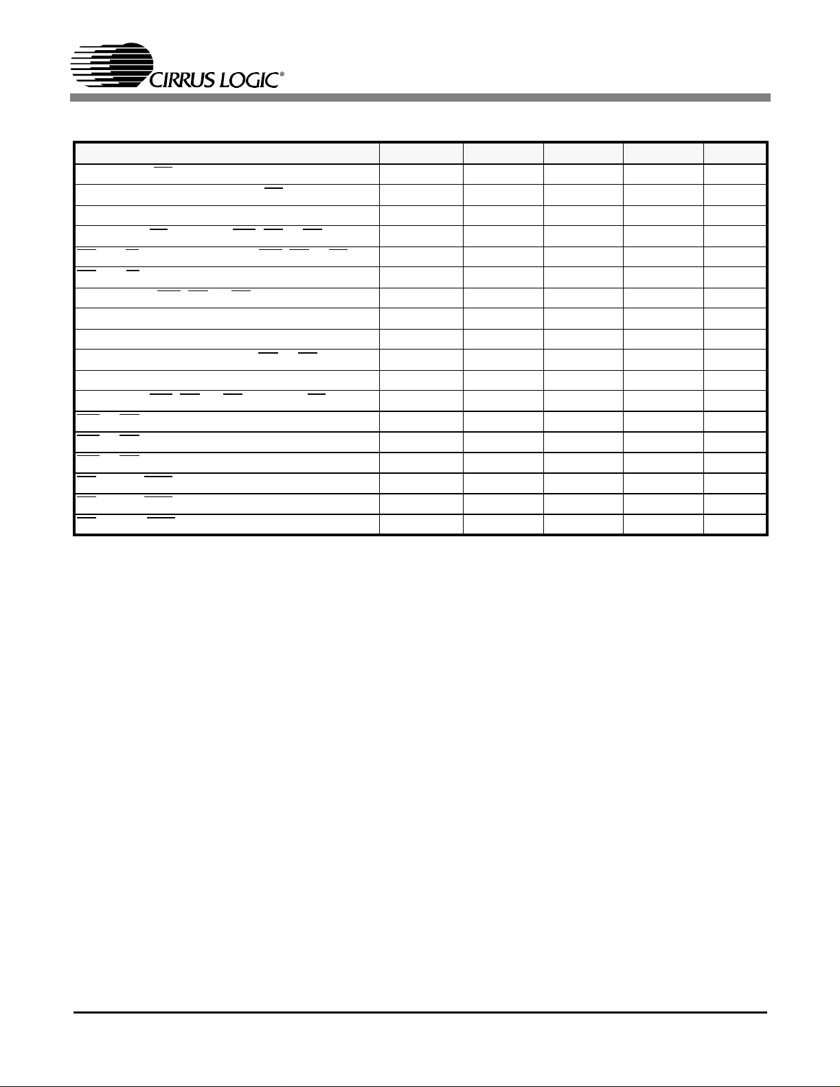
CS61880
19.11 Switching Characteristics - Parallel Port (Multiplexed Mode)
Parameter Ref. # Min. Typ. Max Unit
Pulse Width AS
Muxed Address Setup Time to AS
Muxed Address Hold Time 3 5 - - ns
Delay Time AS
& R/W Setup Time Before WR, RD or DS Low 5 0 - - ns
CS
& R/W Hold Time 6 0 - - ns
CS
Pulse Width, WR
Write Data Setup Time 8 30 - - ns
Write Data Hold Time 9 30 - - ns
Output Da ta D e la y Time fr o m RD
Read Data Hold Time 1 1 5 - - ns
Delay Time WR
or RD Low to RDY Low 13 - - 55 ns
WR
or RD Low to RDY High 14 - - 100 ns
WR
or RD High to RDY HIGH-Z 15 - - 40 ns
WR
Low to ACK High 16 - - 65 ns
DS
Low to ACK Low 17 - - 1 00 ns
DS
High to ACK HIGH-Z 18 - - 40 ns
DS
or ALE High 1 25 - - ns
or ALE Low 2 10 - - ns
or ALE to WR, RD or DS 45--ns
, RD, or DS 770- -ns
or DS Low 10 - - 100 ns
, RD, or DS to ALE or AS Rise 12 30 - - ns
DS450PP3 61
Page 62

ALE
CS61880
1
WR
CS
D[7:0]
RDY
12 4
2
ADDRESS Wr ite Data
HIGH-Z
5
3
7
6
8
14
13
9
15
Figure 25. Parallel Port Timing - Write; Int el® Multip lexed A d d ress / Da ta Bus Mod e
1
HIGH-Z
ALE
RD
CS
D[7:0]
RDY
12 4
2
ADDRESS R ead Data
HIGH-Z
5
3
7
6
10
14
13
11
15
HIGH-Z
Figure 26. Parallel Port Timing - Read; Intel Mult iplexed Addres s / Data Bus Mode
62 DS450PP3
Page 63
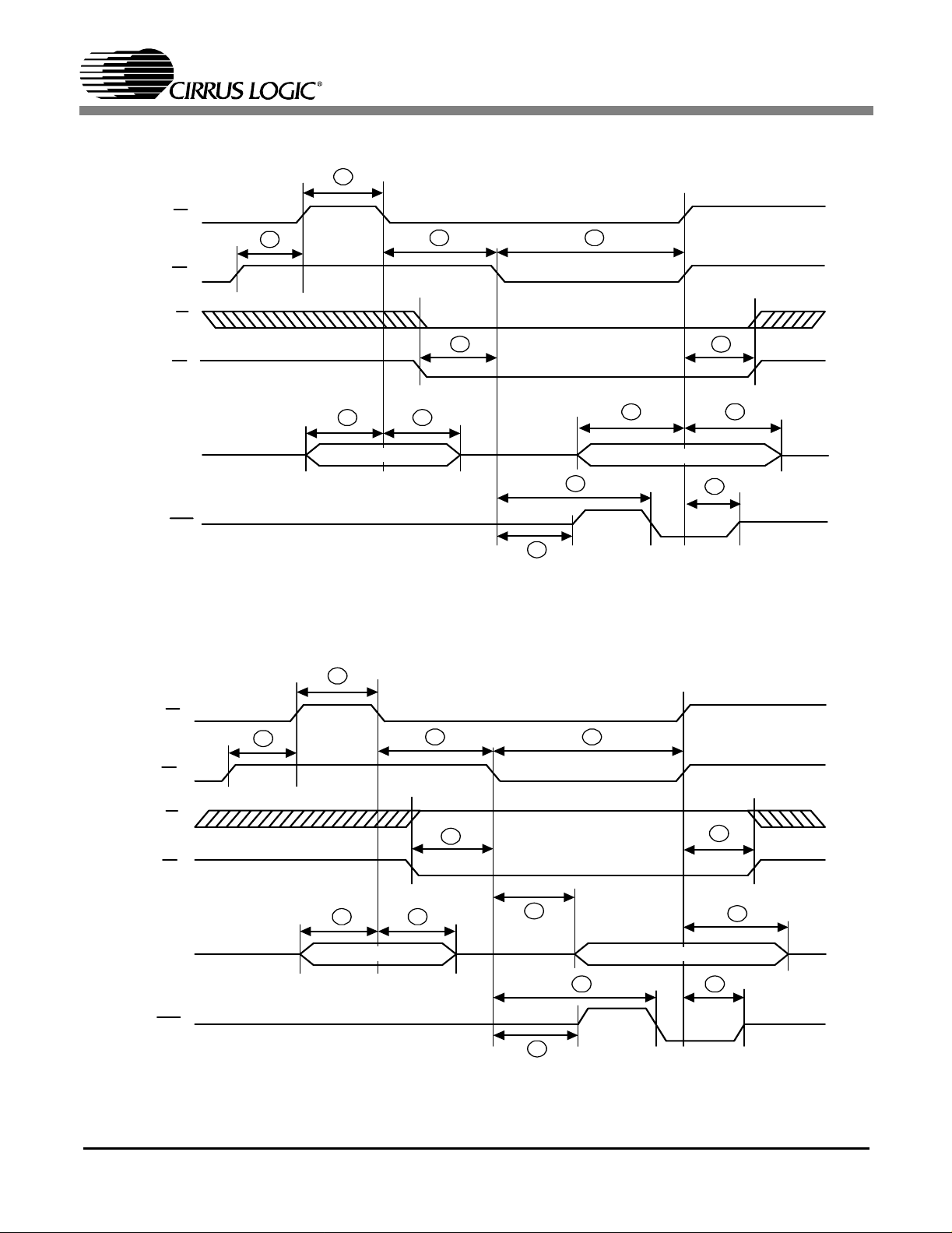
AS
DS
R/W
CS
CS61880
1
12
4
5
7
6
8
Write Data
18
D[7:0]
ACK
2
ADDRESS
HIGH-Z HIGH-Z
3
17
16
Figure 27. Parallel Port Timing - Write; Motorola® Multiplexed Ad dr ess / Data Bus Mode
1
AS
DS
R/W
12
4
5
7
6
9
CS
D[7:0]
ACK
2
ADDRESS
HIGH-Z HIGH-Z
3
10
Read Data
17
16
11
18
Figure 28. Parallel Port Timing - Read; Motor ola Multiplexed Address / Data Bus Mode
DS450PP3 63
Page 64

CS61880
19.12 Switching Characteristics- Parallel Port (Non-Multiplexed Mode)
Parameter Ref. # Min. Typ. Max Unit
Address Setup Time to WR
Address Hold Time 2 5 - - ns
& R/W Setup Time Before WR, RD or DS Low 3 0 - - ns
CS
& R/W Hold Time 4 0 - - ns
CS
Pulse Width, WR
Write Data Setup Time 6 30 - - ns
Write Data Hold Time 7 30 - - ns
Output Da ta D e la y Time fr o m RD
Read Data Hold Time 9 5 - - ns
or RD Low to RDY Low 10 - - 55 ns
WR
, RD or DS Low to RDY High 11 - - 100 ns
WR
, RD or DS High to RDY HIGH-Z 12 - - 40 ns
WR
Low to ACK High 13 - - 65 ns
DS
Low to ACK Low 14 - - 1 00 ns
DS
High to ACK HIGH-Z 15 - - 40 ns
DS
, RD, or DS 570- -ns
, RD or DS Low 1 10 - - ns
or DS 8 - - 100 ns
64 DS450PP3
Page 65

CS61880
2
4
A[4:0]
ALE
WR
CS
D[7:0]
RDY
(pulled high)
HIGH-Z
1
ADDRESS
5
3
6
Write Data
11 12
10
7
Figure 29. Parallel Port Timing - Write; Intel Non-Multiplexed Address / Data Bus Mode
HIGH-Z
2
4
12
A[4:0]
ALE
RD
CS
D[7:0]
RDY
(pulled high)
HIGH-Z
1
ADDRESS
5
3
8
Read Data
11
10
9
Figure 30. Parallel Port Timing - Read; In tel Non-Multiplexed Address / Data Bus Mode
HIGH-Z
DS450PP3 65
Page 66

CS61880
1
A[4:0]
DS
R/W
CS
D[7:0]
ACK
AS
(pulled high)
3 4
HIGH-Z
13
ADDRESS
5
14
6
Write Data
7
15
Figure 31. Parallel Port Timing - Write; Motorola Non-Multiplexed Address / Data Bus Mode
2
HIGH-Z
A[4:0]
AS
DS
R/W
CS
D[7:0]
ACK
1
(pulled high)
HIGH-Z
ADDRESS
5
3 4
8
Read Data
14
13
2
9
15
Figure 32. Parallel Port Timin g - Read; Motorola Non-Multiplexed Address / Data Bus Mode
HIGH-Z
66 DS450PP3
Page 67

19.13 Switching Characteristics - JTAG
Parameter Symbol Min. Max Units
Cycle Time t
TMS/TDI to TCK Rising Setu p Time t
TCK R ising to TMS/TDI Hold Time t
TCK Falling to TDO Valid t
t
cyc
TCK
cyc
su
h
dv
CS61880
200 - ns
50 - ns
50 - ns
-70ns
TMS
TDI
TDO
t
su
Figure 33. JTAG Switching Characteristics
t
h
t
dv
DS450PP3 67
Page 68

20. COMPLIANT RECOMMENDATIONS AND SPECIFICATIONS
CS61880
ETSI ETS 300-011
ETSI ETS 300-166
ETSI ETS 300-233
ETSI TBR 12/13
IEEE 1149.1
ITU-T I.431
ITU-T G.703
ITU-T G.704
ITU-T G.706
ITU-T G.732
ITU-T G.735
ITU-T G.736
ITU-T G.742
ITU-T G.772
ITU-T G.775
ITU-T G.783
ITU-T G.823
ITU-T O.151
OFTEL OTR-001
68 DS450PP3
Page 69

21. 160-BALL FBGA PACKAGE DIMENSIONS
CS61880
Figure 34. 160-Ball FBGA Package Drawing
DS450PP3 69
Page 70

22. 144-PIN LQFP PACKAGE DIMENSIONS
E
E1
D1
D
CS61880
1
e
∝
L
DIM MIN NOM MAX MIN NOM MAX
A --- 0.55 0.063 --- 1.40 1.60
A1 0.002 0.004 0.006 0.05 0. 10 0.15
B 0.007 0.008 0.011 0.17 0.20 0.27
D 0.854 0.866 BSC 0. 878 21.70 22.0 BSC 22.30
D1 0.783 0.787 B SC 0.791 19.90 20.0 BSC 20.10
E 0.854 0.866 BSC 0.878 21. 70 22 .0 BSC 22.30
E1 0.783 0.787 BSC 0.791 19.90 20.0 BSC 20.10
e* 0.016 0.020 0.024 0.40 0.50 BSC 0.60
∝
L 0.018 0.024 0.030 0.45 0.60 0.75
* Nominal pin pitch is 0.50 mm Controlling dimension is mm. JEDEC Designation: MS022
0.000° 4° 7.000° 0.00° 4° 7.00°
B
Figure 35. 144-Pin LQFP Package Drawing
Table 16. 144-Pin Package Dimensions
INCHES MILLIMETERS
A
A1
70 DS450PP3
 Loading...