

Page 1
Copyright Cirrus Logic, Inc. 2005
(All Rights Reserved)
http://www.cirrus.com
CS61584A
Dual T1/E1 Line Interface
SEP ‘05
DS261F1
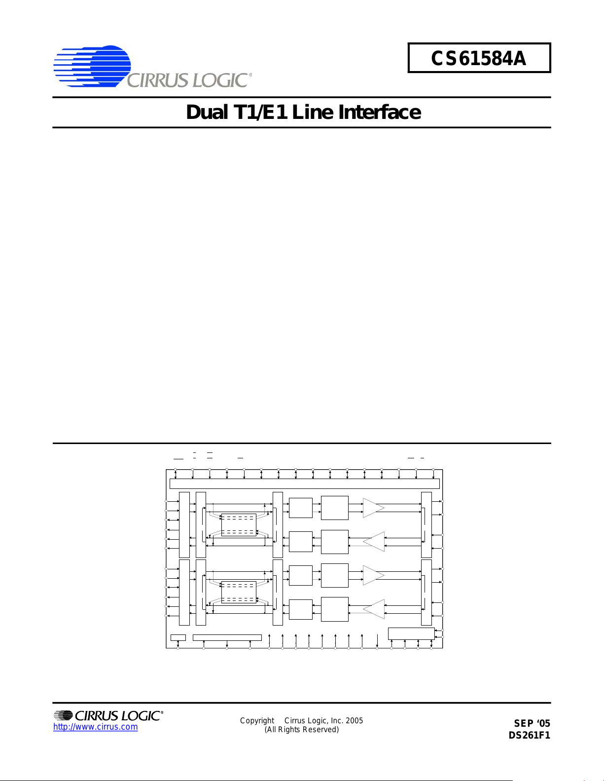
Dual T1/E1 Line Interface
CS61584A
Features
l Dual T1/E1 Line Interface
l 3.3 Volt and 5 Volt Versions
l Crystal-less Jitter Attenuator Meets
European CTR 12 and ETSI ETS 300 011
Specifications
l Matched Impedance Transmit Drivers
l Transmitter Tri-state Capability
l Common Transmit and
ReceiveTransformers for all Modes
l Serial and Parallel Host Mo de Operation
l User-customizable Pulse Shapes
l Supports JTAG Boundary Scan
l Compliant with:
– ITU-T Recommendations: G.703, G.704,
G.706, G.732, G.775 and I.431
– American National Standards (ANSI): T1.102,
T1.105, T1.403, T1.408, and T1.231
– FCC Rules and Regulations: Part 68 and Part
15
– AT&T Publication 62411
– ETSI ETS 300 011, 300 233, CTR 12, TBR 13
l TR-NET-00499
Description
The CS61584A is a dual li ne interface for T1/E 1 applications, designed for high-volume cards where low
power and high density are requ ired. The device is optimized for flexible microprocessor control through a
serial or paralle l Host mode interface. Ha rdware mode
operation is also available.
Matched impedance drivers reduce power consumption
and provide substantial transmitter return loss. The
transmitter pulse shapes are customizable to allow nonstandard line loads . Crystalless jitter a ttenuation complies with most stringent standards. Support of JTAG
boundary scan enhances system testability and
reliability.
ORDERING INFORMATION
See
page 53.
CS61584A-IQ3:3.3V, 64-pin TQFP, -40 to +85° C
CS61584A-IL5:5.0V, 68-pin PLCC, -40 to +85° C
CS61584A-IQ5:5.0V, 64-pin TQFP, -40 to +85° C
Preliminary Product Information
P.O. Box 17847, Austin, Texas 78760
(512) 445 7222 FAX: (512) 445 7581
http://www.cirrus.com
Serial Port
Parallel Port
Hardware Mode
TCLK1
(TDATA1) TPOS1
(AIS1) TNEG1
RCLK1
(RDATA1) RPOS1
(BPV1) RNEG1
TCLK2
(TDATA2) TPOS2
(AIS2) TNEG2
RCLK2
(RDATA2) RPOS2
(BPV2) RNEG2
IPOL
IPOL (DTACK)
CLKE
JTAG
INT
SCLK
SDO
SDI
CS
4
P/S
P/S
ATTEN0
E
N
C
O
D
E
R
D
E
C
O
D
E
R
E
N
C
O
D
E
R
D
E
C
O
D
E
R
INT
RD(DS)
RLOOP2
JITTER
JITTER
AD0
LLOOP
CS
RLOOP1
ATTEN1
R
E
M
O
T
E
L
ATTENUATOR
O
O
P
B
A
C
K
R
E
M
O
T
E
L
ATTENUATOR
O
O
P
B
A
C
K
CLOCK GENERATOR
REFCLK XTALOUT 1XCLK TV+ TGND RV+ RGND DV+ DGND
SPOL
AD1
AD2
TAOS1
TAOS2
CONTROL
L
O
C
A
TAOS
L
L
O
O
P
LOS &
B
A
AIS
C
DETECT
K
1
L
O
C
A
TAOS
L
L
O
O
P
LOS &
B
A
AIS
C
DETECT
K
1
2 2 2 2 3
This document contains information for a new product.
Cirrus Logic reserves the right to modify this product without notice.
Copyright Cirrus Logic, Inc. 2000
AD3
AD4
CON02
PULSE
SHAPING
CIRCUITRY
CLOCK &
DATA
RECOVERY
PULSE
SHAPING
CIRCUITRY
CLOCK &
DATA
RECOVERY
AD5
CON11
AV+ AGND
CON12
CON01
(All Rights Reserved)
AD6
DRIVER
DRIVER
CON21
RECEIVER
RECEIVER
BGREF
AD7
PD1
SAD4
ZTX1
ALE(AS)
CON22
WR(R/W)
CON31
CONTROL
PD2
SAD5
ZTX2
LOS1
SAD6
LOS1
BTS
CON32
L
O
C
A
L
L
O
O
P
B
A
C
K
2
L
O
C
A
L
L
O
O
P
B
A
C
K
2
LOS2
SAD7
LOS2
TTIP1
TRING1
RTIP1
RRING1
TTIP2
TRING2
RTIP2
RRING2
RESET
MODE
Hardware Mode
Parallel Port
Serial Port
JAN ‘01
DS261PP5
1
Page 2

TABLE OF CONTENTS
1. CHARACTERISTICS AND SPECIFICATIONS .................................. ....... ...... ....... ...... ....... ..... 5
ABSOLUTE MAXIMUM RATINGS ...........................................................................................5
RECOMMENDED OPERATING CONDITIONS.......................................................................5
ANALOG CHARACTERISTICS................................................................................................ 6
ANALOG CHARACTERISTICS................................................................................................ 7
DIGITAL CHARACTERISTICS................................................................................................. 8
SWITCHING CHARACTERISTICS . ...... ....... ...... ......................................................................8
SWITCHING CHARACTERISTICS - SERIAL PORT .............................................................10
SWITCHING CHARACTERISTICS - PARALLEL PORT........................................................11
SWITCHING CHARACTERISTICS - JTAG............................................................................ 14
2. OVERVIEW ............................................................................................................................. 15
2.1 AT&T 62411 Customer Premises Application .................................................................. 16
2.2 Asynchronous Multiplexer Application ............................................................................. 16
2.3 Synchronous Application ................................................................................................. 16
3. TRANSMITTER .......................................................................................................................16
4. RECEIVER .............................................................................................................................. 18
5. JITTER ATTENUATOR ................... ...... ....... ...... ....... ...... .......................................................19
6. REFERENCE CLOCK ............................................................................................................20
7. POWER-UP RESET ................................................................................................................20
8. LINE CONTROL AND MONITORING .................................................................................... 20
8.1 Line Code Encoder/Decoder ............................................................................................20
8.2 Alarm Indication Signal ....................................................................................................20
8.3 Bipolar Violation Detection ...............................................................................................21
8.4 Excessive Zeros Detection ..............................................................................................21
8.5 Loss of Signal .................................................................................................................. 21
8.6 Transmit All Ones ............................................................................................................21
8.7 Receive All Ones ............................................................................................................. 21
8.8 Local Loopback ................................................................................................................22
8.9 Remote Loopback ............................................................................................................22
8.10 Driver Tristate ................................................................................................................ 22
8.11 Power Down ................................................................................................................... 22
8.12 Reset Pin ....................................................................................................................... 23
9. HOST MODE ...........................................................................................................................23
9.1 Register Set ..................................................................................................................... 23
9.1.1 Status Registers ..................................................................................................23
DS261PP5
CS61584A
CS61584A
Contacting Cirrus Logic Support
For a complete listing of Direct Sales, Distributor, and Sales Representative contacts, visit the Cirrus Logic web site at:
http://www.cirrus.com/corporate/contacts/sales.cfm
Preliminary product inf o rmation describes products whi c h are i n production, but for whi ch f ul l char act erization data is not yet avai l ab le . Ad vance p roduct infor-
mation describes products which are in development and subject to development changes. Cirrus Logic, Inc. has made best efforts to ensure that the information
contained in this document i s accurat e and reli able. However , t he infor mation is subje ct to chang e without noti ce and is provi d ed “AS IS” without warrant y of
any kind (express or implied). Customers are advised to obtain the latest version of relevant information to verify, before placing orders, that information being
relied on is current and complete. All products are sold subject to the terms and conditions of sale supplied at the time of order acknowledgment, including those
pertaining to warran t y , pa tent infringement, and limitation of liability. N o responsibility is ass umed by Cirrus Logic, In c . for the use of this information, including
use of this inf orma t i on as the basis for manufacture or sale o f any items, nor for i nf ringements of pat en t s or other rights o f thir d parti es. This document i s the
property of Cirrus Logic, Inc. a nd by furni shing th is i nformati on, Cir rus L ogic, In c. grant s no l icense, express or i mpli ed under any patent s, mask work righ ts,
copyrights, trademarks, trad e secrets o r ot her i ntellect ual pro pert y right s of Cirrus L ogic, I nc. Ci rrus L ogic, In c., cop yright owner of the in forma tion co ntaine d
herein, gives consent for copies to be made of the information only for use within your organization with respect to Cirrus Logic integrated circuits or other parts
of Cirrus Logic, Inc. The same consent is gi ven for simi lar inf ormat ion con tai ned on a ny Cirru s Logic we bsite or disk. T his consent does not extend to othe r
copying such as copying for general distribution, advertising or promotional purposes, or for creating any work for resale. The names of products of Cirrus Logic,
Inc. or other vendors and suppliers appearing in this document may be trademarks or service marks of their respective owners which may be registered in some
jurisdictions. A list of Cirrus Logic, Inc. trademarks and service marks can be found at http://www.cirrus.com
2 DS261PP5
2 DS261F1
.
Page 3

DS261PP5
CS61584A
CS61584A
9.1.2 Mask Registers ................................................................................................... 25
9.1.3 Control A Registers ............................................................................................. 26
9.1.4 Control B Registers ............................................................................................. 27
9.1.5 Arbitrary Waveform Registers ............................................................................. 27
9.2 Serial Port Operation ....................................................................................................... 30
9.3 Parallel Port Operation ....................................................................................................31
10. JTAG BOUNDARY SCAN .................................................................................................... 31
10.1 JTAG Data Registers (DR) ............................................................................................ 32
10.2 JTAG Instructions and Instruction Register (IR) ............................................................ 33
10.3 JTAG TAP Controller ..................................................................................................... 33
10.4 Test-Logic-Reset State .................................................................................................. 33
10.5 Run-Test/Idle State ........................................................................................................ 34
10.6 Select-DR-Scan State ................................................................................................... 34
10.7 Capture-DR State ..........................................................................................................34
10.8 Shift-DR State ................................................................................................................ 34
10.9 Exit1-DR State ............................................................................................................... 34
10.10 Pause-DR State ...........................................................................................................35
10.11 Exit2-DR State ............................................................................................................. 35
10.12 Update-DR State ......................................................................................................... 35
10.13 Select-IR-Scan State ................................................................................................... 35
10.14 Capture-IR State .......................................................................................................... 35
10.15 Shift-IR State ............................................................................................................... 35
10.16 Exit1-IR State .............................................................................................................. 36
10.17 Pause-IR State ............................................................................................................ 36
10.18 Exit2-IR State .............................................................................................................. 36
10.19 Update-IR State ........................................................................................................... 36
10.20 JTAG Application Examples ........................................................................................ 36
11. PIN DESCRIPTIONS ............................................................................................................ 39
12. PACKAGE DIMENSIONS .................................................................................................... 46
13. APPLICATIONS ................................................................................................................... 48
13.1 Line Interface ................................................................................................................. 48
13.2 Power Supply ................................................................................................................ 50
13.3 Quartz Crystal Specifications ........................................................................................ 50
13.4 Crystal Oscillator Specifications .................................................................................... 50
13.5 Transformers ................................................................................................................. 51
13.6 Designing for AT&T 62411 ............................................................................................ 51
13.7 Line Protection ............................................................................................................... 51
13.8 Loop Selection Equations .............................................................................................. 51
LIST OF TABLES
Table 1. Line Configuration Selections............................................................................................. 17
Table 3. Jitter Attenuation Control.................................................................................................... 19
Table 4. CS61584A Register Set..................................................................................................... 23
Table 5. Status Registers................................................................................................................. 24
Table 6. Mask Registers................................................................................................................... 25
Table 7. Control A Registers............................................................................................................ 26
Table 8. Control B Registers............................................................................................................ 27
Table 9. Arbitrary Waveform Registers............................................................................................ 28
Table 10. Boundary Scan Register .................................................................................................. 32
Table 11. Device Identifcation Register............................................................................................ 33
Table 12. ......................................................................................................................................... 33
DS261PP5 3
DS261F1 3
Page 4

DS261PP5
Table 13. CS61584A External Components.....................................................................................48
Table 14. Quartz Crystal Specifications ...........................................................................................50
Table 15. Suggested Quartz Crystals...............................................................................................50
Table 16. Suggested Crystal Oscillators ..........................................................................................50
Table 17. Transformer Specifications...............................................................................................51
Table 18. Recommended Transformers........................................................................................... 52
LIST OF FIGURES
Figure 1. Signal Rise And Fall Characteristics ..............................................................................9
Figure 2. Recovered Clock and Data Switching Characteristics ...................................................9
Figure 3. Transmit Clock and Data Switching Characteristics ......................................................9
Figure 4. Serial Port Write Timing Diagram ................................................................................. 10
Figure 5. Serial Port Read Timing Diagram ................................................................................10
Figure 6. Parallel Port Timing - Motorola Mode . ...... ....................................................................12
Figure 7. Parallel Port Timing - Intel Read Mode ........................................................................12
Figure 8. Parallel Port Timing - Intel Write Mode ........... ...... ...... ....... ...... ....... .............................12
Figure 9. Parallel Port Timing - Motorola Mode to RAM . ...... ...... ....... .......................................... 1 3
Figure 10. Parallel Port Timing - Intel Read Mode from RAM or ROM ......................................... 13
Figure 11. Parallel Port Timing - Intel Write Mode to RAM .......... ....... ....................................... ... 13
Figure 12. JTAG Switching Characteristics ................................................................................... 14
Figure 13. Examples of CS61584A Applications ...........................................................................15
Figure 14. Typical Pulse Shape at DSX-1 Cross Connect ............................................................17
Figure 15. Mask of the Pulse at the 2048 kbps Interface ..............................................................17
Figure 16. Minimum Input Jitter Tolerance of Receiver (Clock Recovery Circuit and
jitter Attenuator) ............................................................................................................ 18
Figure 17. Typical Jitter Transfer Function .................................................................................... 19
Figure 18. Alarm Indication Event Relationships ...........................................................................24
Figure 19. Phase Definition of Arbitrary Waveforms .....................................................................29
Figure 20. Example of Summing of Waveforms ............................................................................ 29
Figure 21. Serial Read/Write Format (SPOL = 0) ..........................................................................30
Figure 22. Address Command byte ............................................................................................... 30
Figure 23. JTAG Circuitry Block Diagram ..................................................................................... 31
Figure 24. TAP Controller State Diagram ...................................................................................... 34
Figure 25. JTAG Instruction Register update ................................................................................37
Figure 26. JTAG Data Register update .........................................................................................38
Figure 27. Hardware Mode Configuration ..................................................................................... 48
Figure 28. Host Mode Serial Port Configuration ............................................................................49
Figure 29. Host Mode Parallel Port Configuration ......................................................................... 49
CS61584A
CS61584A
4 DS261PP5
4 DS261F1
Page 5
DS261PP5
CS61584A
CS61584A
1. CHARACTERISTICS AND SPECIFICATIONS
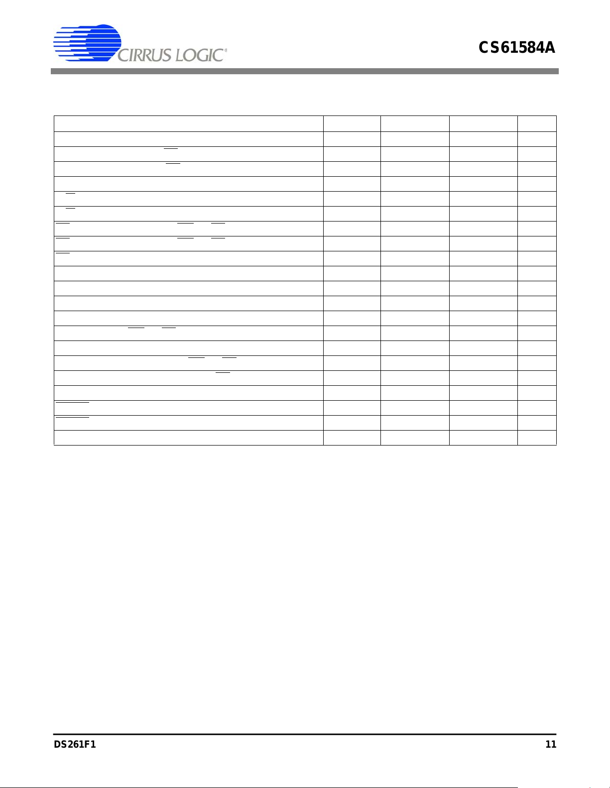
ABSOLUTE MAXIMUM RATINGS
Parameter Symbol Min Max Unit
DC Supply (TV+1, TV+2, RV+1, RV+2, AV+, DV+) (Note 1) - 6.0 V
Input Voltage (Any Pin) V
Input Current (Any Pin) (Note 2) I
Ambient Operating Temperature T
Storage Temperature T
Notes: 1. Referenced to RGND1, RGND2, TGND1, TGND2, AGND, DGND at 0 V.
2. Transient currents of up to 100 mA will not cause SCR latch-up.
WARNING: Operation at or beyond these limits may result in permanent damage to the device.
Normal operation is not guaranteed at these extremes.
in
in
A
stg
RECOMMENDED OPERATING CONDITIONS
Parameter Symbol Min Typ Max Unit
DC Supply (TV+1, TV+2, RV+1, RV+2, AV+, DV+) (Note 3)
3.3 V
5.0 V
Ambient Operating Temperature T
Power Consumption Per Channel (3.3 V) (Note 4)
T1 (Note 5)
T1 (Note 6)
E1, 75 Ω (Note 5)
E1, 120 Ω (Note 5)
Power Consumption Per Channel (5.0 V) (Note 4)
T1 (Note 5)
T1 (Note 6)
E1, 75 Ω (Note 5)
E1, 120 Ω (Note 5)
REFCLK Frequency T1 1XCLK = 1
T1 1XCLK = 0
REFCLK Frequency E1 1XCLK = 1
E1 1XCLK = 0
A
P
C
P
C
RGND - 0.3 (RV+) + 0.3 V
-10 10 mA
-40 85 °C
-65 150 °C
3.135
4.75
-40 25 85 °C
-
-
-
-
-
-
-
-
(1.544 -
100 ppm)
(12.352 -
100 ppm)
(2.048 -
100 ppm)
(16.384 -
100 ppm)
3.3
5.0
310
190
250
230
350
250
320
310
1.544
12.352
2.048
16.384
3.465
5.25
-
-
-
-
-
-
-
-
(1.544 +
100 ppm)
(12.352 +
100 ppm)
(2.048 +
100 ppm)
(16.384 +
100 ppm)
MHz
MHz
MHz
MHz
V
mW
mW
Notes: 3. TV+1, TV+2, AV+, DV+, RV+1, RV+2 should be connected together. TGND1, TGND2, RGND1, GND2,
DGND1, DGND2, DGND3 should be connected together.
4. Per channel power consumption while driving line load over operating temperature range. Includes
device and load. Digital input levels are within 10% of the supply rails and digital outputs are driving a
50 pF capacitive load.
5. Assumes 100% ones density and maximum line length at maximum supply voltage (3.465 V or 5.25 V).
6. Assumes 50% ones density and 300 ft. line length at typical supply voltage (3.3 V or 5.0 V).
Specifications are subject to change without notice
DS261PP5 5
DS261F1 5
Page 6
DS261PP5
CS61584A
CS61584A
ANALOG CHARACTERISTICS (T
Parameter Symbol Min Typ Max Unit
= -40 to 85 °C; power supply pins within ±5% of nominal.)
A
Receiver
RTIP/RRING Differential Input Impedance - 20 - kΩ
Sensitivity Below DSX-1 (0 dB = 2.4 V) - -13.6 - dB
Loss of Signal Threshold - 0.3 - V
Data Decision Threshold T1, DSX-1 (Note 7)
(Note 8)
T1, FCC Part 68 and E1 (Note
9)
(Note 10)
Allowable Consecutive Zeros before LOS 160 175 190 bits
Receiver Input Jitter Tolerance (DSX-1, E1)
10 Hz and bel ow (N ot e 11)
2kHz
10 kHz - 100 kHz
Receiver Return Loss (Notes 12, 13, and 14)
51 kHz - 102 kHz
102 kHz - 2.048 MHz
2.048 MHz - 3.072 MHz
60
55
45
40
300
6.0
0.4
12
18
14
65
50
22
24
22
70
-
-
-
-
-
75
55
60
-
-
-
-
-
-
% of
Peak
UI
dB
Jitter Attenuator
Jitter Attenuator Corner Frequency
T1 (Notes 12 and 15)
E1
Attenuation at 10 kHz Jitter Frequency (Notes 12 and 15) - 60 - dB
Attenuator Input Jitter Tolerance (Note 12)
(Before Onset of FIFO Overflow or Underflow Protection)
1.25
-
28 43 - UI
4.0
1.25
-
-
Hz
pk-pk
Transmitter
Arbitrary Pulse Amplitude at Transformer Secondary
T1, DSX-1
T1, DS1
E1, 75 Ω
E1, 120 Ω
-
-
-
-
73
52
43
52
mV/LS
-
-
-
-
B
Notes: 7. For input amplitude of 1.2 V
8. For input amplitude of 0.5 V
9. For input amplitude of 1.07 V
10. For input amplitude of 4.14 V
11. Jitter tolerance increases at lower frequencies. Refer to the Receiver section.
12. Not production tested. Parameters guaranteed by design and characterization.
13. Typical performance using the line interface circuitry recommended in the Applications section.
14. Return loss = 20 log
= cable impedance.
z
0
15. Attenuation measured with sinusoidal input jitter equal to 3/4 of measured jitter tolerance. Circuit
attenuates jitter at 20 dB/decade above the corner frequency. Output jitter can increase significantly
when more than 28 UI's are input to the attenuator. The jitter attenuator -3 dB knee in T1 mode is
selectable for 4.0 Hz or 1.25 Hz. Refer to the Jitter Attenuator section.
6 DS261PP5
6 DS261F1
ABS((z1 + z0) / (z1 - z0)) where z1 = impedance of the transmitter or receiver, and
10
to 4.14 Vpk.
pk
to 1.2 Vpk, and 4.14 Vpk to 5.0 Vpk.
pk
to 4.14 Vpk.
pk
to 5.0 Vpk.
pk
Page 7

DS261PP5
CS61584A
CS61584A
ANALOG CHARACTERISTICS (Continued)
Parameter Symbol Min Typ Max Unit
Transmitter (Continued)
AMI Output Pulse Amplitudes (Note 16)
E1, 75 Ω (Note 17)
E1, 120 Ω (Note 18)
T1, DSX-1 (Note 19)
Recommended Transmitter Output Load (3.3 V) (Note 16)
T1
E1, 75 Ω
E1, 120 Ω
Recommended Transmitter Output Load (5.0 V) (Note 16)
T1
E1, 75 Ω
E1, 120 Ω
Jitter Added During Remote Loopback
10 Hz - 8 kHz
8kHz - 40kHz
10 Hz - 40 kHz
Broad Band (Note 20)
Power in 2 kHz band about 772 kHz (Notes 12 and 13)
(DSX-1 only)
Power in 2 kHz band about 1.544 MHz (Note 12 and 13)
(referenced to power in 2 kHz band at 772 kHz, DSX-1 only)
Positive to Negative Pulse Imbalance (Notes 12 and 13)
T1, DSX-1
E1, amplitude at center fo pulse interval
E1, width at 50% of nominal amplitude
Transmitter Return Loss (Notes 12, 13, and 14)
51 kHz - 102 kHz
102 kHz - 2.048 MHz
2.048 MHz - 3.072 MHz
E1 Short Circuit Current 5.0 V
3.3 V
E1 and DSX-1 Output Pulse Rise/Fall Times (Note 22) - 50 - ns
E1 Pulse Width (at 50% of peak amplitude) - 244 - ns
E1 Pulse Amplitude for a space E1, 75 Ω
(Note 21)
E1, 120 Ω
2.14
2.7
2.4
-
-
-
-
-
-
-
-
-
-
12.6 15 17.9 dBm
-29 -38 - dB
-
-5
-5
8
14
10
-
-
-0.237
-0.3
2.37
3.0
3.0
24.8
18.6
30.0
76.6
57.4
90.6
0.020
0.015
0.015
0.045
0.2
-
-
25
18
12
-
70
-
-
2.6
3.3
3.6
-
-
-
-
-
-
-
-
-
-
0.5
5
5
-
-
-
50
-
0.237
0.3
mA
mA
V
Ω
Ω
UI
dB
%
%
dB
rms
rms
V
V
Notes: 16. Using a transformer that meets the specifications in the Applications section.
17. Measured across 75 Ω at the output of the transmit transformer for CON3/2/1/0 = 0/0/0/0.
18. Measured across 120 Ω at the output of the transmit transformer for CON3/2/1/0 = 0/0/0/1.
19. Measured at the DSX-1 Cross-Connect for line length settings CON3/2/1/0 = 0/0/1/0, 0/0/1/1, 0/1/0/0,
0/1/0/1, and 0/1/1/0 after the length of #22 ABAM cable specified in Table 1.
20. Input signal to RTIP/RRING is jitter free. Values will reduce slightly if jitter free clock is input to TCLK.
21. Transformer secondary shorted with 0.5 Ω resistor during the transmission of 100% ones.
22. At transformer secondary and measured from 10% to 90% of amplitude.
DS261PP5 7
DS261F1 7
Page 8
DS261PP5
CS61584A
CS61584A
DIGITAL CHARACTERISTICS (T
= -40 to 85 °C; power supply pins within ±5% of nominal.)
A
Parameter Symbol Min Max Unit
High-Level Input Voltage (Note 23) V
Low-Level Input Voltage (Note 23) V
High-Level Output Voltage (I
Low-Level Output Voltage (I
= -40 µA) (Note 24) V
out
= 1.6 mA) (Note 24) V
out
IH
IL
OH
OL
(DV+) - 0.5 - V
-0.5V
(DV+) - 0.3 - V
-0.3V
Input Leakage Current (Digital pins except J-TMS and J-TDI) - ±10 µA
Notes: 23. Digital inputs are designed for CMOS logic levels.
24. Digital outputs are TTL compatible and drive CMOS levels into a CMOS load.
SWITCHING CHARACTERISTICS (T
= -40 to 85 °C; power supply pins within ±5% of nominal;
A
Inputs: Logic 0 = 0 V, Logic 1 = DV+.)
Parameter Symbol Min Typ Max Unit
T1 Clock/Data
TCLK Frequency (Note 25) f
TCLK Duty Cycle t
RCLK Duty Cycle (Note 26) t
pwh2/tpw2
pwh1/tpw1
Rise Time (All Digital Outputs) (Note 27) t
Fall Time (All Digital Outputs) (Note 27) t
RPOS/RNEG (RDATA) to RCLK Rising Setup Time t
RCLK Rising to RPOS/RNEG (RDATA) Hold Time t
TPOS/TNEG (TDATA) to TCLK Falling Setup Time t
TCLK Falling to TPOS/TNEG (TDATA) Hold Time t
tclk
r
f
su1
h1
su2
h2
-1.544-MHz
20 50 80 %
45 50 55 %
- - 65 ns
- - 65 ns
-274-ns
-274-ns
25 - - ns
25 - - ns
E1 Clock/Data
TCLK Frequency (Note 25) f
TCLK Duty Cycle t
RCLK Duty Cycle (Note 26) t
pwh2/tpw2
pwh1/tpw1
Rise Time (All Digital Outputs) (Note 27) t
Fall Time (All Digital Outputs) (Note 27) t
RPOS/RNEG (RDATA) to RCLK Rising Setup Time t
RCLK Rising to RPOS/RNEG (RDATA) Hold Time t
TPOS/TNEG (TDATA) to TCLK Falling Setup Time t
TCLK Falling to TPOS/TNEG (TDATA) Hold Time t
tclk
r
f
su1
h1
su2
h2
-2.048-MHz
20 50 80 %
45 50 55 %
- - 65 ns
- - 65 ns
-194-ns
-194-ns
25 - - ns
25 - - ns
Notes: 25. The maximum burst rate of a gapped TCLK input clock is 8.192 MHz. For the gapped clock to be
tolerated by the CS61584A, the jitter attenuator must be switched to the transmit path of the line
interface. The maximum gap size that can be tolerated on TCLK is 28 UIp-p.
26. RCLK duty cycle may be outside the specified limits when the jitter attenuator is in the transmit path
and when the jitter attenuator is employing the overflow/underflow protection mechanism.
27. At max load of 50 pF.
8 DS261PP5
8 DS261F1
Page 9
DS261PP5
CS61584A
CS61584A
Any Digital Output
RCLK
(for CLKE = high)
RPOS
RNEG
RDATA
BPV
t
r
90% 90%
10% 10%
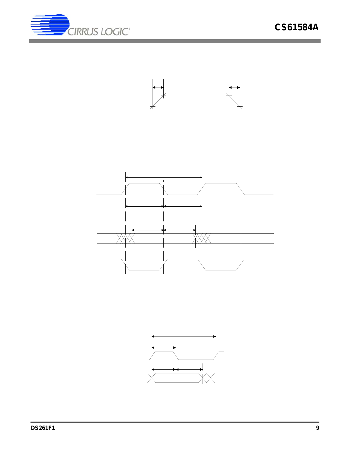
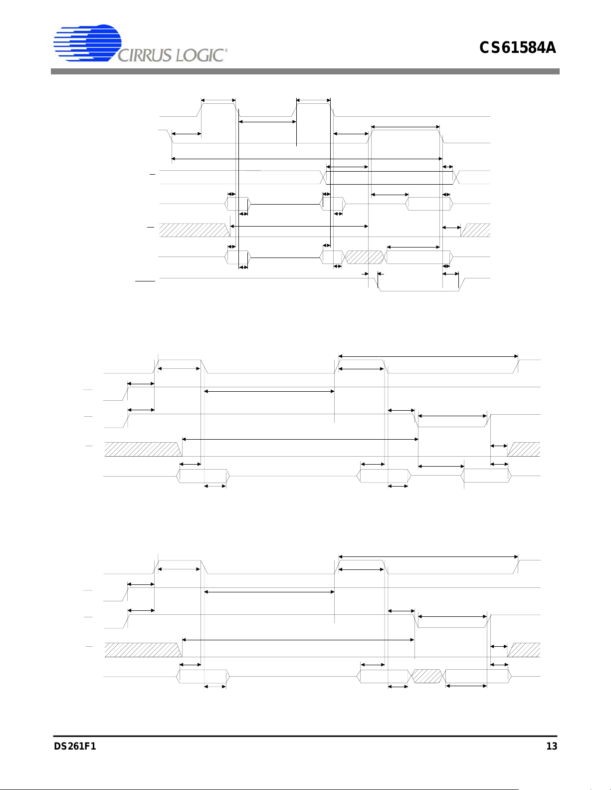
Figure 1. Signal Rise And Fall Characteristics
t
pw1
t
pwl1
t
su1
t
pwh1
t
h1
t
f
RCLK
(for CLKE = low)
Figure 2. Recovered Clock and Data Switching Characteristics
Figure 3. Transmit Clock and Data Switching Characteristics
TCLK
TPOS
TNEG
TDATA
t
pwh2
t
su2
t
pw2
t
h2
DS261PP5 9
DS261F1 9
Page 10
DS261PP5
CS61584A
CS61584A
SWITCHING CHARACTERISTICS - SERIAL PORT (T
nominal ± 0.3 V; Inputs: Logic 0 = 0 V, Logic 1 = RV+)
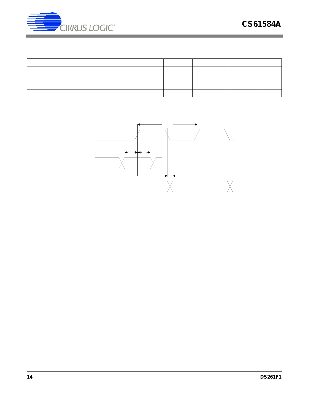
Parameter Symbol Min Typ Max Unit
SDI to SCLK Setup Time t
SCLK to SDI Hold Time t
SCLK Low Time t
SCLK High Time t
SCLK Rise and Fall Time t
CS
to SCLK Setup Time t
SCLK to CS
CS
Inactive Time t
Hold Time (Note 28) t
SDO Valid to SCLK (Note 29) t
CS
to SDO High Z t
Notes: 28. If SPOL = 0, then CS
should return high no sooner than 20 ns after the 16th rising edge of SCLK during
a serial port read.
29. Output load capacitance = 50 pF.
dc
cdh
cl
ch
, t
r
cc
cch
cwh
cdv
cdz
f
= -40 to 85 °C; DV+, TV+, RV+ =
A
25 - - ns
25 - - ns
50 - - ns
50 - - ns
- - 15 ns
20 - - ns
20 - - ns
100 - - ns
- - 50 ns
-50-ns
t
cwh
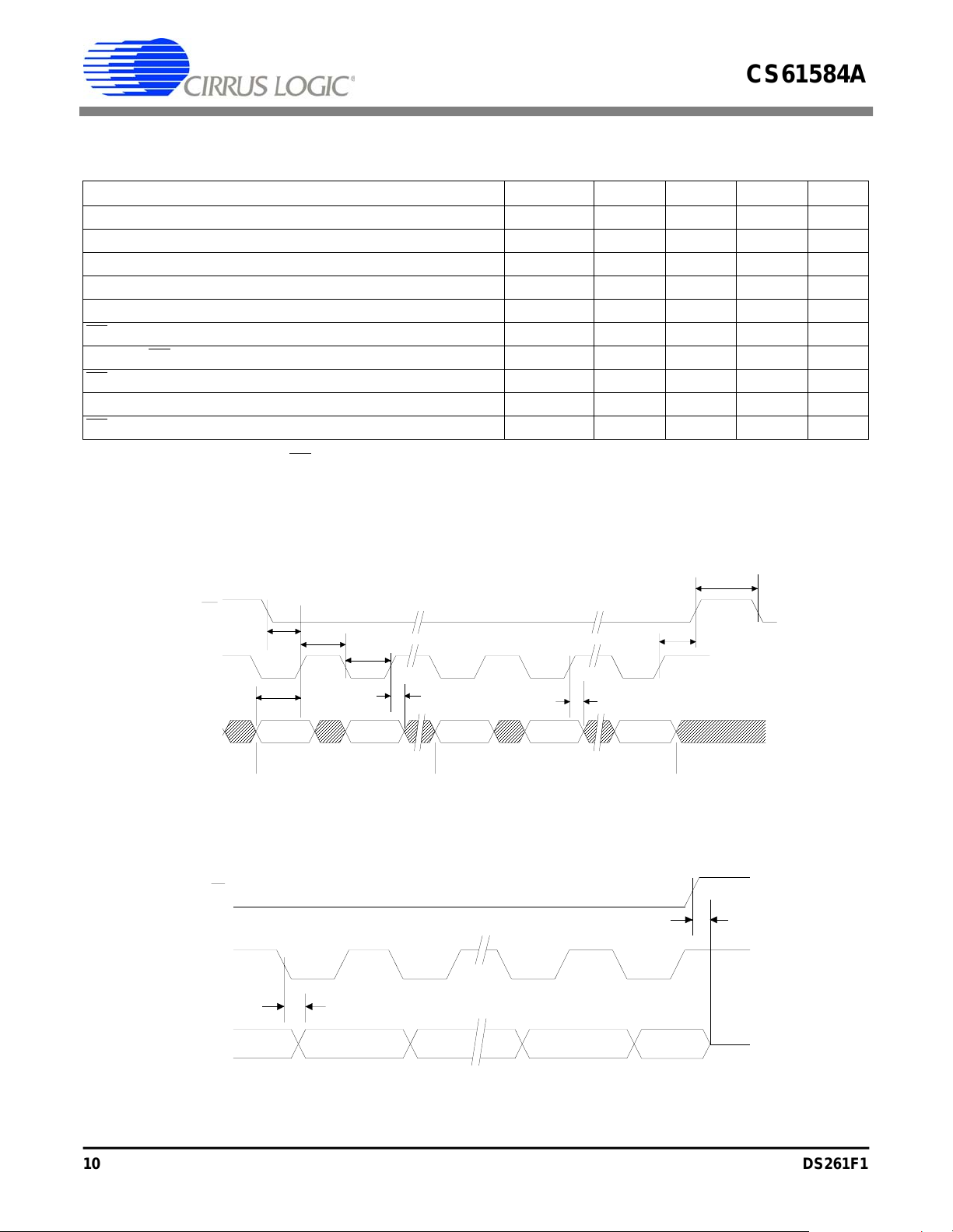
CS
SCLK
SDI
SCLK
SDO
CS
t
ch
t
cc
t
dc
LSB LSB MSB
CONTROL BYTE DATA BYTE
t
cl
t
cdh
t
cdh
Figure 4. Serial Port Write Timing Diagram
t
cdv
t
cch
t
cdz
HIGH
SPOL = 0
Figure 5. Serial Port Read Timing Diagram
10 DS261PP5
10 DS261F1
Page 11
DS261PP5
CS61584A
CS61584A
SWITCHING CHARACTERISTICS - PARALLEL PORT (T
= -40 to 85 °C;
A
TV+, RV+ = nominal ± 0.3 V; Inputs: Logic 0 = 0 V, Logic 1 = RV+)
Parameter Symbol Min Max Unit
Cycle Time t
Pulse Width, DS Low or RD
Pulse Width, DS High or RD
High PW
Low PW
Input Rise/Fall Times t
R/W
Hold Time t
R/W
Setup Time Before DS High t
CS
Setup Time Before DS, WR, or RD Active t
CS
Setup Time Before DS, WR, or RD Active for RAM/ROM t
CS
Hold Time t
Read Data Hold Time t
Write Data Hold Time t
Muxed Address Valid to AS or ALE Fall t
Muxed Address Hold Time t
Delay Time DS, WR
, or RD to AS or ALE Rise t
cyc
, t
r
rwh
rws
cs
csr
ch
dhr
dhw
asl
ahl
asd
el
eh
f
250 - ns
150 - ns
150 - ns
-30ns
10 - ns
50 - ns
50 - ns
130 - ns
20 - ns
10 80 ns
5-ns
15 - ns
10 - ns
25 - ns
Pulse Width AS or ALE High 40 - ns
Delay Time AS or ALE to DS, WR
Output Data Delay Time from DS or RD
Data Setup Time t
DTACK
DTACK
Delay t
Hold Time t
AS/ALE Min Low Interval for RAM/ROM t
, or RD t
ased
t
ddr
dsw
dkd
dkh
aamir
40 - ns
20 120 ns
80 - ns
5-ns
5-ns
50 - ns
DS261PP5 11
DS261F1 11
Page 12
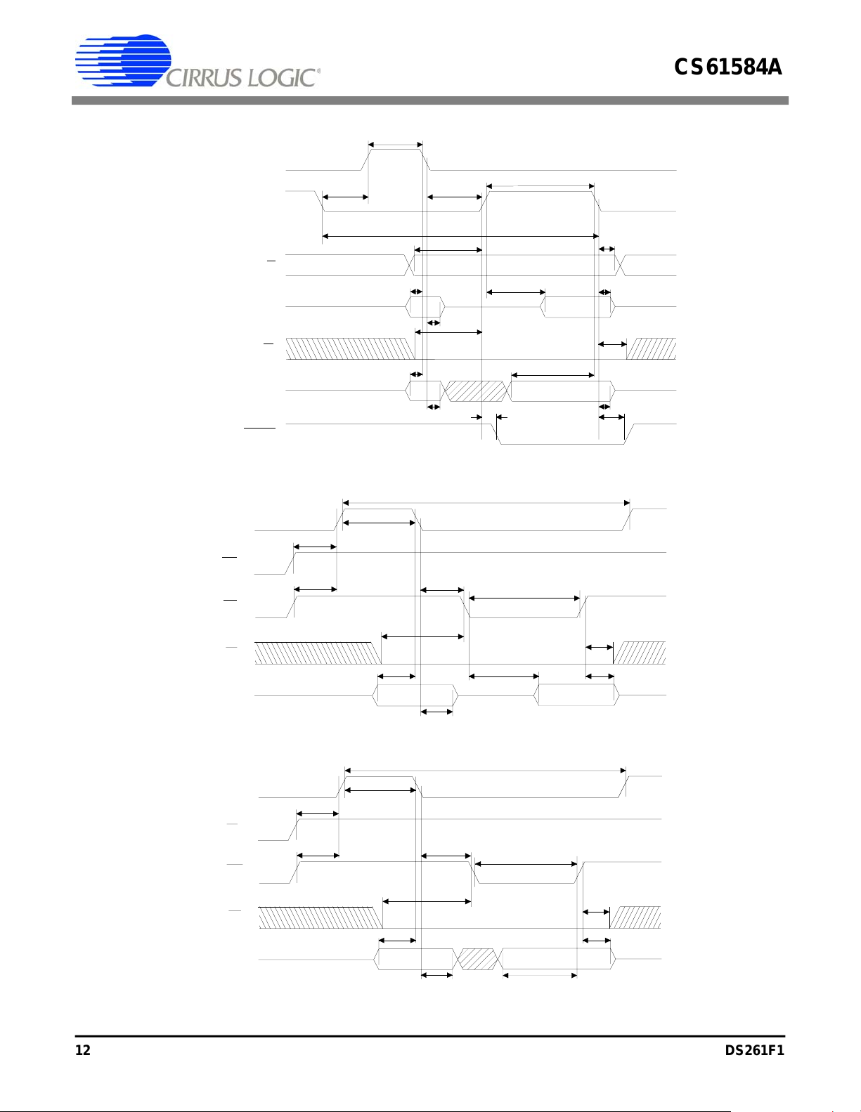
AS
DS
R/W
AD0-AD7
(READ)
CS
AD0-AD7
(WRITE)
(READ and WRITE)
DTACK
DS261PP5
PW
ash
PW
t
asd
t
asl
t
asl
t
ased
t
rws
t
ahl
t
cs
t
ahl
t
dkd
Figure 6. Parallel Port Timing - Motorola Mode
eh
t
cyc
t
ddr
t
dsw
t
dhw
CS61584A
CS61584A
t
rwh
t
dhr
t
ch
t
dkh
ALE
WR
RD
CS
AD0-AD7
ALE
RD
AD0-AD7
WR
CS
t
cyc
PW
t
asd
t
asd
ash
t
ased
t
cs
t
asl
t
ahl
PW
el
t
ddr
Figure 7. Parallel Port Timing - Intel Read Mode
t
cyc
PW
t
asd
t
asd
ash
t
ased
t
cs
t
asl
PW
el
t
ch
t
dhr
t
ch
t
dhw
t
ahl
t
dsw
Figure 8. Parallel Port Timing - Intel Write Mode
12 DS261PP5
12 DS261F1
Page 13
DS261PP5
CS61584A
CS61584A
ALE
WR
RD
CS
AD0-AD7
AS
DS
R/W
AD0-AD7
(READ)
CS
AD0-AD7
(WRITE)
(READ and WRITE)
DTACK
t
asd
t
asd
PW
ash
t
t
asd
t
asl
t
asl
t
ahl
aamir
t
ahl
PW
ash
PW
t
ased
t
rws
t
asl
t
t
csr
t
asl
ahl
t
ahl
eh
t
cyc
t
ddr
t
dsw
t
dkd
t
t
ch
t
dhw
Figure 9. Parallel Port Timing - Motorola Mode to RAM
t
cyc
PW
ash
t
aamir
t
csr
t
asl
t
ahl
PW
ash
t
ased
t
asl
t
ahl
PW
t
ddr
Figure 10. Parallel Port Timing - Intel Read Mode from RAM or ROM
t
rwh
dhr
t
dkh
el
t
ch
t
dhr
t
cyc
ALE
WR
t
asd
t
asd
PW
ash
t
aamir
PW
ash
t
ased
PW
el
RD
t
csr
t
ch
CS
t
asl
t
asl
t
dhr
AD0-AD7
t
t
ahl
t
ahl
dsw
Figure 11. Parallel Port Timing - Intel Write Mode to RAM
DS261PP5 13
DS261F1 13
Page 14
DS261PP5
CS61584A
CS61584A
SWITCHING CHARACTERISTICS - JTAG (T
= -40 to 85 °C; TV+, RV+ = nominal ± 0.3 V;
A
Inputs: Logic 0 = 0 V, Logic 1 = RV+)
Parameter Symbol Min Max Unit
Cycle Time t
J-TMS/J-TDI to J-TCK Rising Setup Time t
J-TCK Rising to J-TMS/J-TDI Hold Time t
J-TCK Falling to J-TDO Valid t
t
cyc
J-TCK
t
t
su
J-TMS
J-TDI
J-TDO
h
cyc
su
h
dv
t
200 - ns
50 - ns
50 - ns
-60ns
dv
Figure 12. JTAG Switching Characteristics
14 DS261PP5
14 DS261F1
Page 15
DS261PP5
CS61584A
CS61584A
2. OVERVIEW
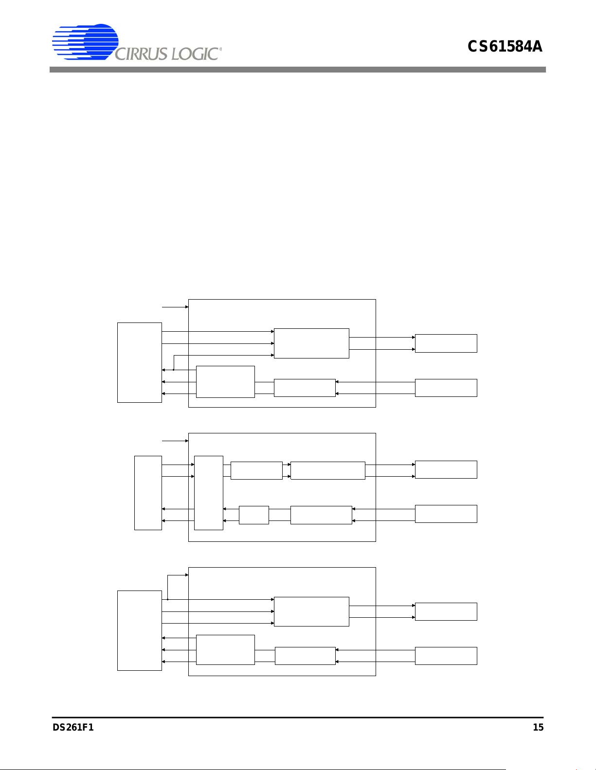
The CS61584A is a dual line interface for T1/E1
applications, designed for high-volume cards
where low power and high density are required.
The device can be operated in either Hardware
mode using control pins or in Host mode using an
internal register set. One board design can support
all T1/E1 short-haul modes by only changing component values in the receive and transmit paths (if
REFCLK and TCLK are connected externally).
Figure 13 illustrates applications of the CS61584A
in various environments.
LOOP TIMED APPLICATION
CS62180B
FRAMER
TPOS
TNEG
TCLK
RCLK
RPOS
RNEG
REFCLK
ATTENUATOR
JITTER
CS61584A
The line driver generates waveforms compatible
with E1 (CCITT G.703), T1 short haul (DSX-1)
and T1 FCC Part 68 Option A (DS1). A single
transformer turns ratio is used for all waveform
types. The driver internally match es the impedance
of the load, providing excellent return loss to insure
superior T1/E1 pulse quality. An additional benefit
of the internal impedance matching is a 50 percent
reduction in power consumption compared to implementing return loss using external resistors that
causes the transmitter to drive the equivalent of two
line loads.
LINE DRIVER
LINE RECEIVER
TTIP
TRING
RTIP
RRING
TRANSMIT
CIRCUITRY
RECEIVE
CIRCUITRY
MUX
CS62180B
FRAMER
TDATA
TCLK
(gapped)
RCLK
RDATA
TCLK
TPOS
TNEG
RCLK
RPOS
RNEG
ASYNCHRONOUS MUX APPLICATION
(i.e., VT1.5 card for SONET or SDH mux)
REFCLK
AMI
B8ZS,
HDB3,
CODER
(Including 62411 systems with multiple T1 lines)
REFCLK
JITTER
ATTENUATOR
CS61584A
JITTER
ATTENUATOR
AIS
DETECT
SYNCHRONOUS APPLICATION
LINE DRIVER
LINE RECEIVER
CS61584A
LINE DRIVER
LINE RECEIVER
Figure 13. Examples of CS61584A Applications
TTIP
TRING
RTIP
RRING
TTIP
TRING
RTIP
RRING
TRANSMIT
CIRCUITRY
RECEIVE
CIRCUITRY
TRANSMIT
CIRCUITRY
RECEIVE
CIRCUITRY
DS261PP5 15
DS261F1 15
Page 16

DS261PP5
CS61584A
CS61584A
The line receiver contains all the necessary clock
and data recovery circuits.
The jitter attenuator meets AT&T 62411 requirements when using either a 1X or 8X reference
clock supplied by either a quartz crystal, crystal oscillator, or external reference at the REFCLK input
pin.
2.1 AT&T 62411 Customer Premises Application
The AT&T 62411 specification applies to the T1
interface between the customer premises and the
carrier, and must be implemented by the customer
premises equipment in order to connect to the
AT&T network.
In 62411 applications, the management of jitter is a
very important design consideration. Typically, the
jitter attenuator is placed in the receive path of the
CS61584A to reduce the jitter input to the system
synchronizer. The jitter attenuated recovered clock
is used as the input to the transmit clock to imple-
ment a loop-timed system. A Stratum 4 (±32 ppm)
quality clock or better should be input to R EFCLK.
Note that any jitter present on the reference clock
will not be filtered by the jitter attenuator.
2.2 Asynchronous Multiplexer Application
Asynchronous multiplexers accept multiple T1/E1
lines (which are asynchronous to each other ), and
combine them into a higher speed tran smission rate
(e.g. M13 muxes and SONET muxes). In these systems, the jitter attenuator is placed in the transmit
path of the CS61584A to remove the gapped clock
jitter input by the multiplexer to TCLK. Because
the transmit clock is jittered, the reference clock to
the CS61584A is provided by an external source
operating at 1X or 8X the data rate. Because T1/E1
framers are not usually required in asynchronous
multiplexers, the B8ZS/AMI/HDB3 coders in the
CS61584A are activated to provide data interfaces
on TDATA and RDATA.
2.3 Synchronous Application
A typical example of a synchronous application is
a T1 card in a central office switch or a 0/1 digital
cross-connect system. These systems place the jitter attenuator in the receive path to reduce the jit ter
presented to the system. A Stratum 3 or better system clock is input to the CS61584A transmit and
reference clocks.
3. TRANSMITTER
The transmitter accepts data from a T1 or E1 system and outputs pulses of appropriate shape to the
line. The transmit clock (TCLK) and transmit data
(TPOS and TNEG, or TDATA) are supplied synchronously. Data is sampled on the falling edge of
the TCLK input.
During Hardware mode operation, the configuration pins (CON[3:0]) control transmitted pulse
shapes, transmitter source impedance, receiver
slicing level, and driver tristate as shown in
Table 1. During Host mode operation, the configuration is established by the CON[3:0] bits in the
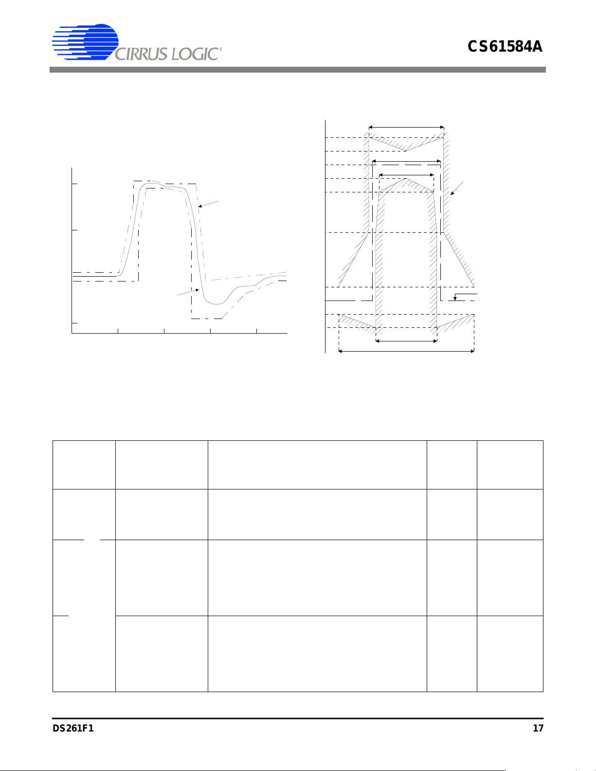
Control B registers. Typical output pulses are
shown in Figures 14 and 15. These pulse shapes are
fully pre-defined by circuitry in the CS61584A,
and are fully compliant with appropriate standards
when used with our application guidelines in standard installations. Both channels must be operated
at the same line rate (both T1 or both E1).
Host mode operation permits arbitrary transmit
pulse shapes to be created and downloaded to the
CS61584A. These custom pulse shapes can be used
to compensate for waveform degradation caused by
non-standard cables, transformers, or protection
circuitry (refer to the Arbitrary Wavefor m Registers section).
Note that the pulse width for Part 68 Option A
(324 ns) is narrower than the optimal pulse width
for DSX-1 (350 ns). The CS61584A automatically
adjusts the pulse width based on the configuration
selection.
16 DS261PP5
16 DS261F1
Page 17
DS261PP5
500
1.0
0.5
0
-0.5
0 250 750 1000
NORMALIZED
AMPLITUDE
ANSI T1.102
SPECIFICATION
CS61584A
OUTPUT
PULSE SHAPE
TIME (nanoseconds)
e
Percent of
nominal
peak
voltage
120
110
100
90
80
50
269 ns
244 ns
194 ns
CS61584A
CS61584A
G.703
Specification
Figure 14. Typical Pulse Shape at DSX-1 Cross Connect
C
C
C
C
Transmit Pulse
O
O
O
O
Width at 50%
N
N
N
N
3
2
1
0
Amplitude
0000 244ns (50%) E1: square, 2.37 V into 75Ω 50% AMI/HDB3
1000 244ns (50%) Arbitrary E1 Wave into 75Ω 50% AMI/HDB3
0001 244ns (50%) E1: square, 2.37 V into 75Ω 50% AMI/HDB3
1001 244ns (50%) Arbitrary E1 Wave into 120Ω 50% AMI/HDB3
0010 350ns (54%) DSX-1: 0-133 ft. 65% AMI/B8ZS
0011 350ns (54%) DSX-1: 133-266 ft. 65% AMI/B8ZS
0100 350ns (54%) DSX-1: 266-399 ft. 65% AMI/B8ZS
0101 350ns (54%) DSX-1: 399-533 ft. 65% AMI/B8ZS
0110 350ns (54%) DSX-1: 533-655 ft. 65% AMI/B8ZS
1010 350ns (54%) Arbitrary DSX-1 Waveform 65% AMI/B8ZS
0111 324ns (50%) DS1: FCC Part 68 Option A with undershoot 65% AMI/B8ZS
1100 324ns (50%) DS1: FCC Part 68 Option A (0 dB) 65% AMI/B8ZS
1011 324ns (50%) Arbitrary DS1 Waveform 65% AMI/B8ZS
1101 Reserved
1110 Transmit Hi Z Tristate TTIP/TRING Driver Outputs 50% AMI/HDB3
1111 Transmit Hi Z Tristate TTIP/TRING Driver Outputs 65% AMI/B8ZS
DS261PP5 17
DS261F1 17
10
0
-10
-20
Figure 15. Mask of the Pulse at the 2048 kbps Interface
Transmit Pulse Shape Receiver
Table 1. Line Configuration Selections
219 ns
488 ns
Slicing
Level
Nominal Puls
Line Code
Encoder /
Decoder
Page 18

DS261PP5
CS61584A
CS61584A
The transmitter impedance changes with the line
length options in order to match the load impedance (75 Ω for E1 coax, 100 Ω for T1, 120 Ω for
E1 shielded twisted pair), providing a minimum of
14 dB return loss for T1 and E1 frequencies during
the transmission of both marks and spaces. This
improves signal quality by minimizing reflections
from the transmitter. Impedance matching also reduces load power consumption by a factor of two
when compared to the return loss achieved by using
external resistors.
The CS61584A driver will automatically detect an
inactive TLCK (i.e., no data clocked to the driver)
or REFCLK input. When either of these conditions
are detected the driver is forced t o the tristate (highimpedance) condition. If the jitter attenuator is in
the transmit path, the driver will tristate after 170 to
182 TCLK clock cycles. If the attenuator is not in
the transmit path, the driver will tristate after 4 to
12 TCLK clock cycles. During Host mode operation, the CLKLOST bit in the Status register goes
high to indicate when the driver is tristated due to
the absence of TCLK or REFCLK. The driver exits
the tristate condition when four clock cycles are input to TCLK. On power-up or reset, the driver is
tristated until REFCLK is present and four clock
cycles are input to TCLK. In Host mode the driver
will have to be taken out of the tristate condition by
writing the CON[3:0]. The driver is not forced to
the tristate condition during remote loopback if
TCLK is absent.
When the transmit configuration established by
CON[3:0], TAOS, or LLOOP changes state, the
transmitter stabilizes within 22 TCLK bit periods.
The transmitter takes longer to stabilize when
RLOOP1 or RLOOP2 is selected because the timing circuitry must adjust to the new frequency from
RCLK.
When the transmitter transformer secondaries are
shorted through a 0.5 Ω resistor, the transmitter
will output a maximum of 50 mA-rms, as required
by the European specification BS6450. This spec is
met for 5.0 V operation only.
4. RECEIVER
The input signal is connected to the receiver
through a step down transformer (1.15:1 for 5 V
and 2:1 for 3.3 V). Data and clock are extracted
from the T1/E1 signal input to the line interface and
to the system. The signal is detected differentially
across the receive transformer and can be recovered over the entire range of short haul cable
lengths. The transmit and receive transformer specifications are identical and are presented in the Applications section. As shown in Table 1, the
receiver slicing level is set at 65% for DS1/DSX-1
short-haul and at 50% for all other applications.
The clock recovery circuit is a second-order phase
locked loop that can tolerate up to 0.4 UI of jitter
from 10 kHz to 100 kHz without generating er rors
(Figure 13). The clock and data recovery circuit is
tolerant of long strings of consecutive zeros and
will successfully recover a 1-in-175 jitter-free line
input signal.
Recovered data at RPOS and RNEG (or RDATA)
is stable and may be sampled using the recovered
clock RCLK. During Hardware mode operation,
CS61584A
300
138
100
PEAK-TO-PEAK
JITTER
(unit intervals)
Figure 16. Minimum Input Jitter Tolerance of Receiver
28
10
.4
.1
(Clock Recovery Circuit and jitter Attenuator)
1
1
AT&T 62411
(1990 Version)
Performance
10 1k 10k
100 100k700
300
JITTER FREQUENCY (Hz)
18 DS261PP5
18 DS261F1
Page 19

DS261PP5
Figure 17. Typical Jitter Transfer Function
CS61584A
CS61584A
the CLKE pin determines the clock polarity where
the output data is stable and valid as shown in
Table 2. During Host mode operation, the polarity
is established by the CLKE bit in the Control A register. When CLKE is low, RPOS and RNEG (or
RDATA) are valid on the rising edge of RCLK.
When CLKE is high, RPOS and RNEG (or RDATA) are valid on the falling edge of RCLK
During Host mode operation, the data at RPOS and
RNEG (or RDATA) may be forced to output an unframed all-ones pattern by setting both the
LLOOP1 and LLOOP2 bits in the Control B register to "1".
CLKE DATA CLOCK Clock edge for
valid data
LOW RPOS, RNEG
or RDATA
HIGH RP OS, RNEG
or RDATA
Table 2. Recovered Data/Clock Options
RCLK
RCLK
RCLK
RCLK
Rising
Rising
Falling
Falling
During Hardware mode operation, the location of
the jitter attenuators for both channels is controlled
by the ATTEN0 and ATTEN1 pins. During Host
mode operation, the location of the jitter attenuators are independent and are controlled by the ATTEN[1:0] bits in the Control A registers. Table 3
shows how these pins are decoded.
The attenuator consists of a 64-bit FIFO, a narrowband monolithic PLL, and control logic. Signal jitter is absorbed in the FIFO which is designed to
neither overflow nor underflow. If overflow or underflow is imminent, the jitter transfer function is
altered to ensure that no bit-errors occur. Under this
condition, jitter gain may occur and exte rnal provisions may be required. The jitter attenuator will
typically tolerate 43 UIs before the overflow/underflow mechanism occurs. If the jitter attenuator
has not had time to "lock" to the average incoming
frequency (e.g. following a device reset) the a ttenuator will tolerate a minimum of 22 UIs before the
overflow/underflow mechanism occurs.
0
10
20
30
40
Maximum
Attenuation
Attenuation in dB
Limit
50
60
1 10 100 1 k 10 k
E1 Mode
Minimum Attenuation Limit
62411 Requirements
T1 Mode
Measured Performance
Frequency in Hz
5. JITTER ATTENUATOR
The jitter attenuator can be switched into ei ther t he
receive or transmit paths. Alternatively, it can also
be removed from both paths to reduce the propagation delay. Figure 14 illustrates the typical jitter attenuation curves.
The jitter attenuator -3 dB knee frequency is 4.0 Hz
for T1 mode and 1.25 Hz for E1 mode as selected
by the CON[3:0] pins or register bits. A 1.25 Hz
knee for the E1 mode guarantees jitter attenuation
compliance to European specifications CTR 12 and
ETSI ETS 300 011. Setting ATTEN[1:0] = 11 will
place the jitter attenuator in the receive path with a
1.25 Hz knee for both T1 and E1 modes of operation.
For T1/E1 line cards used in high-speed mutiplexers (e.g., SONET and SDH), the jitter attenuator is
typically used in the transmit path. The attenuator
can accept a transmit clock with gaps ≤ 28 UIs and
a transmit clock burst rate of ≤ 8 MHz.
ATTEN1 ATTEN0 Location of Jitter Attenuator
00 Receiver
0 1 Disabled
1 0 Transmitter
1 1 Receiver w/ 1.25 Hz knee
Table 3. Jitter Attenuation Control
DS261PP5 19
DS261F1 19
Page 20

DS261PP5
CS61584A
CS61584A
6. REFERENCE CLOCK
The CS61584A requires a reference clock with a
minimum accuracy of ±100 ppm for T1 and E1 applications. This clock can be either a 1X clock (i.e.,
1.544 MHz or 2.048 MHz), or can be a 8X clock
(i.e., 12.352 MHz or 16.384 MHz) as selected by
the 1XCLK pin. This clock may be supplied from
internal system timing or a CMOS crystal oscillator
and input to the REFCLK pin. An 8X quartz crystal
may be connected across the REFCLK and XTALOUT pins and the 1XCLK pin set low. The quartz
crystal and CMOS crystal oscillator specifications
and are presented in the Applications section.
In systems with a jittered transmit clock, the reference clock should not be tied to the transmit clock
and a separate external quartz crystal or crystal oscillator should drive the reference clock input. Any
jitter present on the reference clock will not be filtered by the jitter attenuator.
7. POWER-UP RESET
On power-up, the device is held in a static state until the power supply achieves approximately 60%
of the power supply voltage. When this threshold is
crossed, the device waits another 10 ms to allow the
power supply to reach operating voltage and then
calibrates the transmit and receive circuitry. This
initial calibration takes less than 20 ms but can occur only if REFCLK and TCLK are present.
Power-up reset initializes the control logic and register set and performs the same functions as the RESET pin. During Host mode operation, a reset event
is indicated by the Latched-Reset bit in the Status
register.
8. LINE CONTROL AND MONITORING
Line control and monitoring of the CS61584A may
be implemented in either Hardware or Host mode.
Hardware mode is selected when the MODE pin is
set low and allows the device to be configured and
monitored using control pins. Host mode is selected when the MODE pin is set high and allows the
device to be configured and monitored using an internal register set.
The following controls and indications are available in Hardware mode: line length selection, receive clock edge, jitter attenuator location, loss of
signal, transmit all ones, local loopback, remote
loopback, and power down. Host mode operation
offers several additional control options (refer to
the Host Mode section).
Note: Please refer to the Loop Selection Equations in
the Applications section.
8.1 Line Code Encoder/Decoder
Hardware mode supports only transparent operation to permit the line code to be encoded and decoded by an external T1/E1 framing device.
Recovered data is output on the RNEG and RPOS
pins in NRZ format and transmitted data is input on
the TNEG and TPOS pins.
Host mode supports transparent, AMI, B8ZS, or
HDB3 line encoding and decoding for applications
not using an external T1/E1 framer (i.e. multiplexers). The CODER, AMI-T, and AMI-R bits in the
Control A registers select the coder mode for a given channel. The selection of the transmit encoder is
independent from the selection of the receive decoder. When CODER = 1, the transmit data is input
to the encoder on TDATA and the receive data is
output from the decoder on RDATA in NRZ format.
8.2 Alarm Indication Signal
During Host mode operation, the alarm indication
signal (AIS) is detected by the receiver and reported using the AIS and Latched-AIS bits in the Status
registers. The receiver detects the AIS condition on
observation of 99.9% ones density in a 5.3 ms period (< 9 zeros in 8192 bits). If CODER = 1 in the
Control A registers, the TNEG pin becomes the
AIS output pin that is set high on detection of AIS.
The AIS condition is exited when ≥ 9 zeros are detected in 8192 bits.
20 DS261PP5
20 DS261F1
Page 21

DS261PP5
CS61584A
CS61584A
8.3 Bipolar Violation Detection
During Host mode operation, a bipolar violation
(BPV) is detected by the receiver and reported using the Latched-BPV bit in the Status registers. If
CODER = 1 in the Control A registers, the RNEG
pin becomes the BPV output strobe pin that is set
high for one bit period on detection of a BPV. Note
that B8ZS (or HDB3) zero substitutions are not
flagged as bipolar violations if the B8ZS (or
HDB3) decoder has been enabled (CODER = 1 and
AMI-R = 0 in the Control A registers).
8.4 Excessive Zeros Detection
During Host mode operation if CODER = 1 and
EXZ = 1 in the Control A register, the BPV output
pin is OR’ed with receive excessive zero events. In
AMI mode when AMI-Rx = 1, the BPV pin is set
high for one bit period when 16 or more consecutive zeros are received. In B8ZS mode when AMIRx = 0, the BPV pin is set high for one bit period
when 8 or more consecutive zeros are received.
This is in accordance with the ANSI T1.231 specification. For E1 operation with HDB3 disabled, the
excessive zeros detection is also disabled. For E1
with HDB3 enabled the BPV pin goes high for every set of 4 consecutively received zeros.
8.5 Loss of Signal
During Hardware mode and Host mode operation,
the loss of signal (LOS) condition is detected by the
receiver and reported when the LOS pin is set high.
Loss of signal is indicated when 175 ±15 consecutive zeros are received, or when the receive
(R TIP/RRING) signal level drops below the receiver sensitivity of the device. The LOS condition is
exited according to the ANSI T1.231-1993 criteria
that requires a minimum 12.5% ones density signal
over 175 ±75 bit periods with no more than 100
consecutive zeros. During LOS, recovered data is
squelched and zeroes are output on RPOS/RNEG
(RDATA).
During Host mode operation, LOS is reported using the LOS and Latched-LOS bits in the Status
registers. Note that both the LOS pin and register
indications are available in Host mode operation.
The LOS pin and/or bit is set high when the device
is reset, in power-up, or a channel is powered-down
and returns low when data is recovered by the receiver.
During LOS condition the RPOS (RDATA),
RNEG pins are forced low, except when LLOOP1
(digital loopback) is enabled, or when the AAO
(Automatic All Ones) bit is set in the channel 1
mask register. Setting the AAO bit high forces unframed all ones pattern out on the RPOS (RDATA), RNEG pins when LOS condition occurs.
When the jitter attenuator is in th e rece ive path and
LOS occurs, the frequency of the last valid recovered signal is held at RCLK. When the jitter attenuator is not in the receive path, the output
frequency becomes the frequency of the reference
clock.
8.6 Transmit All Ones
During Hardware mode operation, transmit all ones
(TAOS) is selected by setting the TAOS pin high.
During Host mode, TAOS is controlled using the
TAOS bit in the Control B registers.
Selecting TAOS causes continuous ones to be
transmitted to the line on TTIP and TRING at the
frequency of REFCLK. In this mode, the transmit
data inputs TPOS and TNEG (or TDATA) are ignored. A TAOS request overrides the data tran smitted to the line interface during local and remote
loopbacks. Note that the CLKLOST interrupt is
not available for TCLK in the TAOS mode.
8.7 Receive All Ones
During Host mode operation, the data at RPOS and
RNEG (or RDATA) may be forced to output an unframed all-ones pattern by setting both the
LLOOP1 and LLOOP2 bits in the Control B register to "1". An automatic Receive All Ones (AAO)
DS261PP5 21
DS261F1 21
Page 22

DS261PP5
CS61584A
CS61584A
response to a Loss of Signal condition for either
channel is activated by setting bit 1 of the channel
1 Mask register to 1.
8.8 Local Loopback
Selecting LLOOP causes the TCLK, TPOS, and
TNEG (or TDATA) inputs to be looped back
through the jitter attenuator (if enabled) to the
RCLK, RPOS, and RNEG (or RDATA) outputs.
The receive line interface is ignored, but data at
TPOS and TNEG (or TDATA) continues to be
transmitted to the line interface at TTIP and
TRING. During Hardware mode operation, simultaneous local loopback 2 of both channels is selected by setting the LLOOP pin high. During Host
mode operation, local loopback 1 on a per channel
basis is controlled using the LLOOP1 bit in the
Control B registers.
During Hardware mode operation, a per channel local loopback 1 is performed when both the RLOOP
and TAOS pins are high. The data at TPOS and
TNEG is overridden with an all-ones pattern (TAOS)
and the receive input at RTIP and RRING is ignored.
During Host mode operation, local loopback 2 can
also be selected using the LLOOP2 bit in the Control
B registers. Selecting LLOOP2 causes the TCLK,
TPOS, and TNEG (or TDATA) inputs to be looped
back to the RCLK, RPOS, and RNEG (or RDATA)
outputs. The line driver, line receiver, and jitter attenuator (if enabled) are also included. The receive
line interface is ignored, but data at TPOS and
TNEG (or TDATA) continues to be transmitted to
the line interface at TTIP and TRING.
A TAOS request overrides the data transmitted to
the line interface during both local loopbacks. A
TAOS request also overrides the data received at
RPOS and RNEG (or RDATA) during local loopback 2. Note that simultaneous selection of local
and remote loopback modes is not valid.
8.9 Remote Loopback
During Hardware mode operation, remote loopbacks of either channel is selected by setting the
RLOOP pin high. During Host mode operation, remote loopback of each channel is controlled using
the RLOOP bit in the Control B registers.
Selecting RLOOP causes the data received from
the line interface at RTIP and RRING to be looped
back through the jitter attenuator (if enabled) and
retransmitted on TTIP and TRING. Data input to
TPOS and TNEG (or TDATA) is ignored, but data
recovered from RTIP and RRING continues to be
output on RPOS and RNEG (or RDATA).
Remote loopback is functional if TCLK is absent.
A TAOS request overrides the data transmitted to
the line interface during a remote loopback. Note
that simultaneous selection of local and remote
loopback modes is not valid.
8.10 Driver Tristate
The drivers may be independently tristated in all
modes of oper ation. During Hardware mode operation, setting the CON[3:0] pins of a channel to
"111X" will tristate the driver. During Host mode serial port operation, t he ZTX1 and ZTX2 pins perform
the driver tristate function and setting the CON[3:0]
bits in the Control B registers to "111X" will also
tristate the driver. During Host mode parallel port operation, setting the CON[3:0] bits in the Control B
register to "111X" tristates the driver. In host mode,
the CS61584A powers up with CON[3:0] set to
1110, which tristates the transmitter.
8.11 Power Down
During Hardware mode operation, channel power
down is selected by setting the PD1 or PD2 pin
high. During Host mode operation, channel power
down is controlled using the PD bit in the Control
A registers. Power down places the transmitter, receiver, and jitter attenuator in reset. The RCLK,
RPOS, RNEG, RDATA, AIS, BPV, TTIP, and
TRING output pins are placed in a high-impedance
22 DS261PP5
22 DS261F1
Page 23

DS261PP5
CS61584A
CS61584A
state. LOS will go high, and the status register will
be reset, but the Control, Mask, and Arbitrary
Waveform registers remain unchanged. The channel not in power down and the processor port will
still to operate normally.
Simultaneously selecting PD1 and PD2 will place
all the above-mentioned pins in high impedance
state and power down additional analog circuitry
that is shared by both channels. The status registers
are reset. In the hardware mode all output pins are
tri-stated and internally pulled up to the positive
supply rail. After exiting the power down state, the
channel will be fully operational in less than 20 ms.
8.12 Reset Pin
The CS61584A is continuously calibrated during
operation to insure the performance of the device
over power supply and temperature. This continuous calibration function eliminates the need to reset
the line interface during operation.
During Hardware and Host modes of opera tion, a
device reset is selected by setting the RESET pin
high for a minimum of 200 ns. The reset function
initiates on the falling edge of RESET and requires
less than 20 ms to complete. The control logic and
register set are initialized and the transmit and receive circuitry is calibrated if REFCLK and TCLK
are present. During Host mode operation, a reset
event is indicated by the Latched-Reset bit in the
Status register.
9. HOST MODE
Host mode allows the CS61584A to be configured
and monitored using an internal register set. This
option is selected when the MODE pin is set high.
Using the P/S pin, serial or 8-bit para llel interface
ports are available in Host mode. During serial port
operation, the registers are specified by a 6-bit address in the range of 0x10 to 0x19. During parallel
port operation, the registers are specified by an 8bit address. The four most significant bits of the address selects one of 16 devices on the board, estab-
lished by the SAD[7:4] pins. The four least
significant bits of the address specify the register
address in the range of 0x00 to 0x09 for the selected
device. Parallel port option is compatible with Motorola and Intel 8-bit, multiplexed address/data bus.
9.1 Register Set
The register set available during Host mode operation is presented in Table 4.
Serial Po rt
Address
0x10 0xY0 Ch 1 Status
0x11 0xY1 Ch 2 Status
0x12 0xY2 Ch 1 Mask
0x13 0xY3 Ch 2 Mask
0x14 0xY4 Ch 1 Control A
0x15 0xY5 Ch 2 Control A
0x16 0xY6 Ch 1 Control B
0x17 0xY7 Ch 2 Control B
0x18 0xY8 Ch 1 Arbitrary Pulse Shape
0x19 0xY9 Ch 2 Arbitrary Pulse Shape
*Y denote s the SAD[7:4] addre ss of the CS61584A device.
Parallel Port
Address*
Table 4. CS61584A Register Set
Description
9.1.1 Status Registers
The Status registers are read-only registers and are
shown in Table 5. The CS61584A generates an interrupt on the INT pin any time an unmasked Status
register bit changes. When BTS is low (Intel
mode), the IPOL pin determines the polarity of the
pin. When BTS is high (Motorola mode), INT
INT
polarity is active low (IPOL becomes DTACK).
Reading both Status register clears the interrupt
and deactivates the INT pin.
LOS: Set high while the loss of signal condition is
detected. Reading the Status register does not clear
the LOS bit. A LOS interrupt is generated only on
the falling edge of the LOS alarm condition. The
Latched-LOS bit generates an interrupt on the rising edge of LOS. Refer to the timing diagram in
Figure 18.
DS261PP5 23
DS261F1 23
Page 24

DS261PP5
CS61584A
CS61584A
Latched-LOS: Set high on the rising edge of the
loss of signal condition. Reading the Status register
clears the Latched-LOS bit and deactivates the INT
pin. Refer to the timing diagram in Figure 18.
AIS: Set high while the alarm indication signal is
the AIS bit. An AIS interrupt is generated only on
the falling edge of the AIS alarm condition. The
Latched-AIS bit generates an interrupt on the rising
edge of AIS. Refer to the timing diagram in
Figure 18.
detected. Reading the Status register does not clear
Status Register (Channel 1)
Serial Port Address: 0x10; Parallel Port Address: 0xY0
Bit Description Definition Reset
10
7 LOS1 LOS currently detected no LOS 1
6 Latched-LOS1 LOS event since last read no LOS 1
5 AIS1 AIS currently detected no AIS 0
4 Latched-AIS1 AIS event since last read no AIS 0
3 Latched-BPV1 BPV event since last read no BPV 0
2 Latched-Overflow1 Pulse overflow since last read no overflow 0
1 Latched-Reset Reset event since last read no reset 1
0 Interrupt1 Interrupt event since last read no interrupt 1
Status Register (Channel 2)
Serial Port Address: 0x11; Parallel Port Address: 0xY1
Bit Description Definition Reset
10
7 LOS2 LOS currently detected no LOS 1
6 Latched-LOS2 LOS event since last read no LOS 1
5 AIS2 AIS currently detected no AIS 0
4 Latched-AIS2 AIS event since last read no AIS 0
3 Latched-BPV2 BPV event since last read no BPV 0
2 Latched-Overflow2 Pulse overflow since last read no overflow 0
1 Latched-CLKLOST TCLK or REFCLK absent TCLK and REFCLK present 0
0 Interrupt2 Interrupt event since last read no interrupt 1
Table 5. Status Registers
Value
Value
AIS/LOS Currently Active
(AIS/LOS bit & AIS/LOS pi n)
Latched LOS
(Latch AIS/LOS bit)
Interrupt
(INT)
Read AIS/LOS bits
Figure 18. Alarm Indication Event Relationships
24 DS261PP5
24 DS261F1
"Short" AIS/LOS event
Set by start
of AIS/LOS
Set by Change
of AIS/LOS
"Long" AIS/LOS event
Cleared by read
Cleared by read
Page 25

DS261PP5
CS61584A
CS61584A
Latched-AIS: Set high on the rising edge of the
alarm indication signal condition. Reading the Status register clears the Latched-AIS bit and deactivates the INT pin. Refer to the timing diagram in
Figure 18.
Latched-BPV: Indicates a bipolar violation has
been received since the last read of the Status register. Reading the Status register clears the
Latched-BPV bit and deactivates the INT
pin. This
bit is set only when the line code decoder is enabled
in the Control A register.
Latched-Overflow: Indicates a waveform generated using the Arbitrary Waveform register has exceeded full scale since the last read of t he Status
register. Reading the Status register clears the
Latched-Overflow bit and deactivates the INT pin.
Latched-Reset: Indicates a reset event (power-up or
RESET pin) has occurred since the last read of the
Status register. Reading the Status register clears
the Latched-Reset bit and deactivates the INT pin.
This bit is not maskable.
Latched-CLKLOST: Set high when TCLK or REFCLK are absent. Reading the Status register clears
the Latched-CLKLOST bit and deactivates the INT
pin.
Interrupt: Indicates a cha nge in the Status registe r
since the last read. Reading the Status register
clears the Interrupt bit and deactivates the INT
pin.
9.1.2 Mask Registers
The Mask registers are read-write registers and are
shown in Table 6. The Mask registers disables the
interrupts in the corresponding Status register on a
per-bit basis. Masking a Status register bit forces it
to remain at zero and prevents the INT pin from activating on the condition.
Mask Register (Channel 1)
Serial Port Address: 0x12; Parallel Port Address: 0xY2
Bit Description Definition Reset
10
7 Mask LOS1 Mask Interrupt Enable Interrupt 0
6 Mask Latched-LOS1 Mask Interrupt Enable Interrupt 0
5 Mask AIS1 Mask Interrupt Enable Interrupt 0
4 Mask Latched-AIS1 Mask Interrupt Enable Interrupt 0
3 Mask Latched-BPV1 Mask Interrupt Enable Interrupt 0
2 Mask Latched-Overflow1 Mask Interrupt Enable Interrupt 0
1 Automatic All Ones, AAO Ones at RPOS/NEG on LOS Zeros at RPOS/NEG on LOS 0
0 Mask Interrupt1 Mask Interrupt Enable Interrupt 0
Mask Register (Channel 2)
Serial Port Address: 0x13; Parallel Port Address: 0xY3
Bit Description Definition Reset
10
7 Mask LOS2 Mask Interrupt Enable Interrupt 0
6 Mask Latched-LOS2 Mask Interrupt Enable Interrupt 0
5 Mask AIS2 Mask Interrupt Enable Interrupt 0
4 Mask Latched-AIS2 Mask Interrupt Enable Interrupt 0
3 Mask Latched-BPV2 Mask Interrupt Enable Interrupt 0
2 Mask Latched-Overflow2 Mask Interrupt Enable Interrupt 0
1 Mask Latched-CLKLOST Mask Interrupt Enable Interrupt 0
0 Mask Interrupt2 Mask Interrupt Enable Interrupt 0
Table 6. Mask Registers
Value
Value
DS261PP5 25
DS261F1 25
Page 26

DS261PP5
CS61584A
CS61584A
AAO: The Automatic All-Ones (AAO) bit in the
Mask Register (Channel 1, bit 1) causes an unframed all-ones pattern to be output at the RPOS
and RNEG (or RDATA) pins when the recei ver is
in a loss of signal (LOS) condition.
9.1.3 Control A Registers
CODER: Controls the coder mode function. The
TPOS, TNEG, RPOS, and RNEG pins are active
when the transparent mode is enabled. The TDATA, RDATA, AIS, and BPV pins are active when
the coder mode is enabled.
AMI-T: Controls the line encoder in the transmit
direction. The selection of B8ZS or HDB3 is deter-
The Control A registers are read-write registers and
are shown in Table 7. The Control A registers se-
mined by the CON[3:0] bits (See the Transmitter
section).
lect device configuration and power down control.
AMI-R: Controls the line decoder in the receive di-
CLKE: Establishes the edge of the of RCLK that
RPOS and RNEG (or RDATA) are valid.
PD: Controls per channel power down.
ATTEN0 and ATTEN1: Controls the jitter attenu-
ator location and -3 dB knee frequency (See Jitter
Attenuator section).
Control A Register (Channel 1)
Serial Port Address: 0x14; Parallel Port Address: 0xY4
Bit Description Definition Reset
10
7 CLKE RPOS/RNEG (or RDATA) valid on
falling edge of RCLK
6 PD1 Power down channel Power up channel 0
5 ATTEN01 Jitter attenuator location
4ATTEN11 0
3 CODER1 Coder mode enabled Transparent mode enabled 0
2 AMI-T1 AMI encoder enabled B8ZS/HDB3 encoder enabled 0
1 AMI-R1 AMI decoder enabled B8ZS/HDB3 decoder enabled 0
0 Factory Test Test Normal operation 0
(See Jitter Attenuator section)
rection. The selection of B8ZS or HDB3 is determined by the CON[3:0] bits (See the Transmitter
section).
EXZ: Controls the automatic detection of exce ssive
zeros on the BPV pin according to ANSI T1.231
when coder mode is enabled (CODERx = 1).
RPOS/RNEG (or RDATA) valid on
rising edge of RCLK
Value
0
0
Control A Register (Channel 2)
Serial Port Address: 0x15; Parallel Port Address: 0xY5
Bit Description Definition Reset
10
7 EXZ Excessive zeros de tecti on for both
channels enabled
6 PD2 Power down channel Power up channel 0
5 ATTEN02 Jitter attenuator location
4ATTEN12 0
3 CODER2 Coder mode enabled Transparent mode enabled 0
2 AMI-T2 AMI encoder enabled B8ZS/HDB3 encoder enabled 0
1 AMI-R2 AMI decoder enabled B8ZS/HDB3 decoder enabled 0
0 Factory Test Test Normal operation 0
Table 7. Control A Registers
26 DS261PP5
26 DS261F1
(See Jitter Attenuator section)
Excessive zeros detection for both
channels disabled
Value
0
0
Page 27

DS261PP5
CS61584A
CS61584A
Factory Test: Must be cleared for normal device
operation.
9.1.4 Control B Registers
The Control B registers are read-write registers and
are shown in Table 8. The Control B registers select
device configuration and loopback control.
TAOS: Controls the transmission of all ones to the
line interface. A TAOS request overrides the data
transmitted to the line interface during local and remote loopbacks.
RLOOP: Controls the remote loopback function for
the channel.
LLOOP1: Controls the local loopback #1 function
for the channel. Includes the jitter attenua tor, if enabled. In host mode, selecting LLOOP1 and
LLOOP2 simultaneously causes all ones to be output from RPOS/RNEG (RDATA).
LLOOP2: Controls the local loopback #2 function
for the channel. Includes the line driver, line receiver, and jitter attenuator, if enabled. See LLOOP1,
above, for receive all ones function.
CON[3:0]: Controls the configuration of the line
driver, line receiver, coder, and driver tristate as
shown in the Transmitter section. Both channels
must be configured to operate at the same rate (both
T1 or both E1).
9.1.5 Arbitrary Waveform Registers
In addition to the predefined T1 and E1 pulse
shapes, arbitrary pulse shapes may be crea ted during Host mode operation using the registers shown
in Table 9. This flexibility can be used to compen-
Control B Register (Channel 1)
Serial Port Address: 0x16; Parallel Port Address: 0xY6
Bit Description Definition Reset
10
7 TAOS1 Enable transmit all ones Disable transmit all ones 0
6 RLOOP1 Enable remote loopback Disable remote loopback 0
5 LLOOP11 Enable local loopback #1 Disable local loopback #1 0
4 LLOOP21 Enable local loopback #2 Disable local loopback #2 0
3 CON31 Line configuration selections
2CON21 1
1CON11 1
0CON01 0
Control B Register (Channel 2)
Serial Port Address: 0x17; Parallel Port Address: 0xY7
Bit Description Definition Reset
7 TAOS2 Enable transmit all ones Disable transmit all ones 0
6 RLOOP2 Enable remote loopback Disable remote loopback 0
5 LLOOP12 Enable local loopback #1 Disable local loopback #1 0
4 LLOOP22 Enable local loopback #2 Disable local loopback #2 0
3 CON32 Line configuration selections
2CON22 1
1CON12 1
0CON02 0
Table 8. Control B Registers
(See Transmitter section)
10
(See Transmitter section)
Value
1
Value
1
DS261PP5 27
DS261F1 27
Page 28

DS261PP5
CS61584A
CS61584A
sate for waveform degradation that may result from
non-standard cables, transformers, or protection
circuitry.
Arbitrary waveform generation is enabled when the
CON[3:0] line configuration selection in the Control B register is set to one of four arbitrary waveform modes (See the Transmitter section). The
arbitrary pulse shape of mark (a transmitted "1") is
specified by describing the pulse shape across three
Unit Intervals (UIs). One UI in DS1 applications is
648 ns (1.544 MHz period) and one UI in E1 applications is 488 ns (2.048 MHz period). For example,
arbitrary waveform generation allows the DSX-1
return-to-zero "tail" to extend further into the next
UI or allows T1 long-haul waveforms to be defined
across all three UIs. The ampli tude of a space (a
transmitted "0") is fixed at zero volts.
All three UIs are divided into 14 equal phases for a
total of 42 phase segments. The shape of the pulse
is then defined by writing the amplitude of each
phase segment to the Arbitrary Waveform register
42 times in sequence from UI1/phase1 to
UI3/phase14. The custom pulse shape must be defined using the Arbitrary Waveform register before
setting the CON[3:0] configuration selection to one
of the arbitrary generation settings (i.e., 1001,
1010, or 1011).
For DS1 applications, the CS61584A divides the
648 ns UI into 14 equal phases of 46.3 ns. For
DSX-1 applications, the 648 ns UI is divided into
13 equal phases of 49.8 ns. The phase amplitude information written for phase 14 of each UI is ignored. For E1 applications, the 488 ns UI is divided
into 12 equal phases of 40.7 ns. The phase ampli-
Arbitrary Waveform Register (Channel 1)
Serial Port Address: 0x18; Parallel Port Address: 0xY8
Bit Description Definition Reset
10
70
6MSB
5
4
3
2
1
0LSB
Arbitrary Waveform Register (Channel 2)
Serial Port Address: 0x19; Parallel Port Address: 0xY9
Bit Description Definition Reset
7 0
6MSB
5
4
3
2
1
0LSB
Table 9. Arbitrary Waveform Registers
Arbitrary pulse shape definitions undefined
10
Arbitrary pulse shape definitions undefined
Value
Value
28 DS261PP5
28 DS261F1
Page 29

DS261PP5
E1 Arbitrary Waveform Example
DSX-1 (5 4% duty c yc le ) Ar bi trary Wa v ef o rm Ex amp le
DS-1 (50% duty cycle) Arbitrary Waveform Example
Figure 19. Phase Definition of Arbitrary Waveforms
CS61584A
CS61584A
tude information written for phases 13 and 14 of
each UI is ignored. Examples of arbitrary waveforms are illustrated in Figure 19.
The amplitude of each phase segment is described
by a 7-bit, 2’s complement number (bit 8 is ignored). A positive value describes pulse amplitude
and a negative value describes pulse undershoot.
For DSX-1 applications with CON[3:0] = 1010, the
typical output voltage step is 73 mV/LSB across
the secondary (line side) of the transformer. For
DS1 applications with CON[3:0] = 1011, the typical output voltage step is 52 mV/LSB across the
transformer secondary. For E1 75 Ω coaxial appli cations with CON[3:0] = 1000, the typical output
voltage step is 43 mV/LSB. For E1 120 Ω twistedpair applications with CON[3:0] = 1001, the typical output voltage step is 52 mV/LSB.
The full scale positive value is 0x3F and the full
scale negative value is 0x40. It is recommended
that the output voltage across the secondary of the
transformer (line interface side) be limited to
4.4 Vpk. At higher output voltages, the transmitter
may not be able to drive the requested voltage
based on the current operating conditions.
Because the transmitter drives either a mark or a
space to the line interface ever y UI, the phase amplitude information defined in UI2 and UI3 is added to the symbols transmitted at TTIP and TRING
in those intervals. Therefore, a mark defined only
for UI1 will be output exactly as programmed if another mark is transmitted in the next two UI. However, a mark defined over UI1 and UI2 with an
extended return-to-zero "tail" will cause the leading edge of a mark transmitted in the next UI to rise
or fall more quickly. This is illustrated i n Figure 20.
If the hexadecimal sum of the phase amplitudes exceeds the full scale values, the sum is replaced by
the full scale value and the Latched-Overflow bit is
set in the Status register.
DS261PP5 29
DS261F1 29
Figure 20. Example of Summing of Waveforms
Page 30

DS261PP5
CS61584A
CS61584A
9.2 Serial Port Operation
Serial port operation in Host mode is selected when
the MODE pin is set high and the P/S pin is set low.
In this mode, the CS61584A register set is accessed
by setting the chip select (CS) pin low and communicating over the SDI, SDO, and SCLK pins. Timing over the serial port is independent of the
transmit and receive system timing. Figure 21 illustrates the format of serial port data transfers.
A read or write is initiated by writing an address/command byte (ACB) to SDI. During a read
cycle, the register data addressed by the ACB is
output on SDO on the next eight SCLK clock cycles. During a write cycle, the data byte immediately follows the ACB. A second address byte is
required when reading or writing the Arbitrary
Waveform registers (see below).
Data is written to and read from the serial port in
LSB first format. When writing to the port, SDI input data is sampled by the device on the rising edge
of SCLK. The polarity of the data output on SDO is
controlled by the SPOL pin. When the SPOL pin is
low, data on SDO is valid on the rising edge of
SCLK. When the SPOL pin is high, data on SDO is
valid on the falling edge of SCLK. The SDO pin is
high impedance when not transmitting data. If the
host processor has a bi-directional I/O port, SDI
and SDO may be tied together.
As illustrated in Figure 22, the ACB consists of a
R/W bit, address field, and two reserved bits. The
R/W bit specifies if the current register acc ess is a
read (R/W = 1) or a write (R/W = 0) operation. The
address field specifies the register address from
0x10 to 0x19. The reserved bit must be cleared for
normal operation of serial mode.
During register addressing, the first eight registers
are addressed as 0x10 to 0x17 in the address field
of the ACB. Because Arbitrary Waveform registers
0x18 and 0x19 access multiple bytes of RAM,
reading or writing these registers requires an Address Command Byte followed by a RAM address
byte for each data transfer. The ACB specifies either 0x18 or 0x19 in the address field to access the
channel 1 or channel 2 Arbitrary Waveform register set. The RAM address is an 8-bit, unsigned binary number in the range of 0x00 to 0x29 to
identify one of 42 RAM locations. The data byte
containing the 7-bit, 2’s complement number specifying the phase amplitude completes the 24 SCLK
write cycle.
CS
SCLK
Data Input
SDI
SDO
B7 (MSB)B6B5B4B3B2B1B0
Reserved Reserved ADR4 ADR3 ADR2 ADR1 ADR0 R/W
0 0 MSB Address Field LSB
30 DS261PP5
30 DS261F1
R/W
00
Address/Command Byte(s)
Figure 21. Serial Read/Write Format (SPOL = 0)
00 01 0
Figure 22. Address Command byte
D7D6D5D4D3D2D1D0
Data Output
D6D5D4D3D2D1D0 D7
0 = Write
1 = Read
Page 31

DS261PP5
CS61584A
CS61584A
9.3 Parallel Port Operation
Parallel port operation in Host mode is selected
when the MODE and P/S pins are set high. In this
mode, the CS61584A register set is accessed using
an 8-bit, multiplexed bi-directional address/data
bus AD[7:0]. Timing over the serial port is independent of the transmit and receive system timing.
The device is compatible with both Intel and Motorola bus formats. The Intel bus format is select ed
when the BTS pin is low and the Motorola bus format is selected when the BTS pin is high. A read or
write is initiated by writing an address byte to
AD[7:0]. The device latches the address on the falling edge of ALE(AS). During a read cycle, the register data is output during the later portion of the
RD or DS pulses. The read cycle is terminated and
the bus returns to a high impedance state as RD
transitions high in Intel timing or DS transitions
low in Motorola timing. During a write cycle, valid
write data must be present and held stable during
the later portion of the WR or DS pulses. A second
address byte is required when reading or writing
the Arbitrary Waveform registers (see below).
A read or write over the parallel port is initiated by
writing an address byte to AD[7:0]. The address
byte consists of two nibbles. The four most significant bits AD[7:4] select one of 16 CS61584A devices in the application. This device address value
is established by the SAD[7:4] pins. The four least
significant bits AD[3:0] are the register address for
the selected device, ranging from 0x00 to 0x09.
The first eight device registers are addressed from
0x00 to 0x07 in the four least significant bits of the
address. Because Arbitrary Waveform registers
0x08 and 0x09 access multiple bytes of RAM,
reading or writing these registers requires an additional RAM address byte for each data transfer.
The RAM address is an 8-bit, unsigned binary
number in the range of 0x00 to 0x29 to identify one
of 42 RAM locations. The data byte containing the
7-bit, 2’s complement number specifying the phase
amplitude completes a write cycle. The sequence
for writing to RAM is: first ALE(AS) addresses the
device, a second ALE(AS) addresses the RAM,
then a RD or WR (R/W) accesses the RAM data.
10.JTAG BOUNDARY SCAN
Board testing is supported through JTAG boundary
scan. Using boundary scan, the integrity of the digital paths between devices on a circuit board can be
verified. This verification is supported by the ability to externally set the signals on the digital output
pins of the CS61584A, and to externally read the
signals present on the input pins of the CS61584A.
Additionally, the manufacturer ID, part number
and revision of the device can be read during board
test using JTAG boundary scan.
As shown in Figure 23, the JTAG hardware c onsists of data and instruction registers plus a Test
Access Port (TAP) controller. Control of the TAP
is achieved through signals applied to the Test
Mode Select (J-TMS) and Test Clock (J-TCK) input pins. Data is shifted into the registers via the
Test Data Input (J-TDI) pin, and shifted out of the
registers via the Test Data Output (J-TDO) pin.
Both J-TDI and J-TDO are clocked at a rate determined by J-TCK. The Instruction register defines
which data register is accessed in the shift operation. Note that if J-TDI is floating, an internal pullup resistor forces the pin high.
Digital output pins Digital input pins
parallel latched
output
Boundary Scan Data Register
J-TDI
J-TCK
J-TMS
Figure 23. JTAG Circuitry Block Diagram
Device ID Data Register
Bypass Data Register
Instruction (shift) Register
parallel latc hed
output
TAP
Controller
JTAG Block
MUX
J-TDO
DS261PP5 31
DS261F1 31
Page 32

DS261PP5
CS61584A
CS61584A
10.1 JTAG Data Registers (DR)
The test data registers are the Boundary-Scan Register (BSR), the Device Identification Register
(DIR), and the Bypass Register (BR).
Boundary Scan Register: The BSR is connected in
parallel to all the digital I/O pins, and provides the
mechanism for applying/reading test patterns
to/from the board traces. The BSR is 62 bits long
and is initialized and read using the instruction
SAMPLE/PRELOAD. The bit ordering for the
BSR is the same as the top-view package pin out,
beginning with the LOS1 pin and moving counterclockwise to end with the PD1 pin as shown in Table 10. Note that the analog, oscillator, power,
ground, CLKE/IPOL, and MODE pins are not included as part of the boundary-scan register.
The input pins require one bit in the BSR and only
one J-TCK cycle is required to load test data for
each input pin.
The output pins have two bits in the BSR to define
output high, output low, or high impedance. The
first bit (shifted in first) selects between an outputenabled state (bit set to 1) or high-i mpedanc e sta te
(bit set to 0). The second bit shifted in contains the
test data that may be output on the pin. Therefore ,
two J-TCK cycles are required to load test data for
each output pin.
The bi-directional pins have three bits in the BSR
to define input, output high, output low, or high impedance. The first bit shifted into the BSR configures the output driver as high-impedance (bit set to
0) or active (bit set to 1). The second bit shifted into
the BSR sets the output value when the first bit is 1.
The third bit captures the value of the pin. This pin
may have its value set externally as an input (if the
first bit is 0) or set internally as an output (if the
first bit is 1). To configure a pad as an input, the JTDI pattern is 0X0. To configure a pad as an output, the J-TDI pattern is 1X1. Therefore, three JTCK cycles are re quired to lo ad test data for eac h
bi-directional pin.
When JTAG testing is conducted in Host mode, the
polarity of the INT
pin is determined by the state of
the IPOL pin. The JTAG BSR should configure the
INT pin as an input in Hardware mode and as an
output in Host mode.
Device Identification Register: The DIR provides
the manufacturer, part number, and version of the
CS61584A. This information can be used to verify
that the proper version or revision number has been
used in the system under test. The DIR is 32 bits
long and is partitioned as shown in Table 11. Data
from the DIR is shifted out to J-TDO LSB first.
BSR Bits Pin Name Pad Type
0 - 2 LOS1, SAD6 bi-directional
3 - 5 TNEG1, AIS1 bi-directional
6 TPOS1, TDATA1 input
7TCLK1input
8 - 9 RNEG1, BPV1 output
10 - 11 RPOS1, RDATA1 output
12 - 13 RCLK1 output
14 A TTEN1, CS
15 - 17 RLOOP1, INT
18 RLOOP2, SCLK, RD
19 - 21 LLOOP, SDO, AD0 bi-directional
22 - 24 TAOS1, SDI, AD1 bi-directional
25 - 27 TAOS2, SPOL, AD2 bi-directional
28 - 30 CON01, AD3 bi-directional
31 - 33 CON02, AD4 bi-directional
34 - 36 CON11, AD5 bi-directional
37 - 39 CON12, AD6 bi-directional
40 - 42 CON21, AD7 bi-directional
43 CON22, ALE(AS) input
44 CON31, WR
45 - 46 RCLK2 output
47 - 48 RPOS2, RDATA2 output
49 - 50 RNEG2, BPV2 output
51 TCLK2 input
52 TPOS2, TDATA2 input
53 - 55 TNEG2, AIS2 bi-directional
56 - 58 LOS2, SAD7 bi-directional
59 CON32, BTS input
60 PD2, SAD5 i nput
61 PD1, SAD4 i nput
Table 10. Boundary Scan Register
(DS) input
(R/W) input
input
bi-directional
32 DS261PP5
32 DS261F1
Page 33

DS261PP5
CS61584A
CS61584A
MSB LSB
31 28 27 12 11 1 0
00000110011011100001000011001001
4 bits 16 bits 11 bits
BIT #(s) Function Total Bits
31-28 Version Number 4
27-14 Part Number 14
13-12 Derivative Code 2
11-1 Manufacturer Number 11
0 Constant Logic ‘1’ 1
Table 11. Device Identification Register
Bypass Register: The Bypass register consists of a
single bit, and provides a serial path between J-TDI
and J-TDO, bypassing the BSR. This allows bypassing specific devices during certain board-level
tests. This also reduces test access times by reducing the total number of shifts required from J-TDI
to J-TDO.
10.2 JTAG Instructions and Instruction Register (IR)
SAMPLE/PRELOAD Instruction: The SAMPLE/PRELOAD instructions allows scanning of
the boundary-scan register without interfering with
the operation of the CS61584A. This instruction
connects the BSR to the J-TDI and J-TDO pins.
The normal path between the CS61584A logic and
its I/O pins is maintained. The signals on the I/O
pins are loaded into the BSR. Additionally, this instruction can be used to latch values into the digital
output pins.
IDCODE Instruction: The IDCODE instruction
connects the device identification register to the JTDO pin. The IDCODE instruction is forced into
the instruction register during the Test-Logic-Reset
controller state.The default instruction is IDCODE
after a device reset.
BYPASS Instruction: The BYPASS instruction
connects the minimum length bypass register between the J-TDI and J-TDO pins and allows data to
be shifted in the Shift-DR controller state.
The instruction register (2 bits) allows the instruction to be shifted into the JTAG circuit. The instruction selects the test to be performed or the data
register to be accessed or both. The valid instructions are shifted in LSB first and are listed in
Table 12:
IR CODE INSTRUCTION
00 EXTEST
01 SAMPLE/PRELOAD
10 IDCODE
11 BYPASS
Table 12.
EXTEST Instruction: The EXTEST instruction allows testing of off-chip circuitry and board-level
interconnect. EXTEST connects the BSR to the JTDI and J-TDO pins. The normal path between the
CS61584A logic and I/O pins is broken. The signals on the output pins are loaded from the BSR
and the signals on the input pins are loaded into the
BSR.
10.3 JTAG TAP Controller
Figure 24 shows the state diagram for the TAP state
machine. A description of each state follows. Note
that the figure contains two main branches to access either the data or instructio n registers. The value shown next to each state transition in this figure
is the value present at J-TMS at each rising edge of
J-TCK.
10.4 Test-Logic-Reset State
In this state, the test logic is disabled to continue
normal operation of the device. During initialization, the CS61584A initializes the instruction register with the IDCODE instruction.
Regardless of the original state of the controller,
the controller enters the Test-Logic-Reset state
when the J-TMS input is held high for at least five
rising edges of J-TCK. The controller remains in
this state while J-TMS is high. The CS61584A processor automatically enters this state at power-up.
DS261PP5 33
DS261F1 33
Page 34

DS261PP5
CS61584A
CS61584A
10.5 Run-Test/Idle State
This is a controller state between scan operations.
Once in this state, the controller remains i n the state
as long as J-TMS is held low. The instruction register and all test data registers retain their previous
state. When J-TMS is high and a rising edge is applied to J-TCK, the controller moves to the SelectDR state.
10.6 Select-DR-Scan State
This is a temporary controller state and the instruction does not change in this state. The test data register selected by the current instruction retains its
previous state. If J-TMS is held low and a rising
edge is applied to J-TCK when in this state, the
controller moves into the Capture-DR state and a
scan sequence for the selected test data register is
initiated. If J-TMS is held high and a rising edge
applied to J-TCK, the controller moves to the Select-IR-Scan state.
10.7 Capture-DR State
In this state, the Boundary Scan Register ca ptures
input pin data if the current instruction is EXTEST
or SAMPLE/PRELOAD. The instruction does not
change in this state. The other test data registers,
which do not have parallel input, are not changed.
When the TAP controller is in this state and a rising
edge is applied to J-TCK, the controller enters the
Exit1-DR state if J-TMS is high or the Shift-DR
state if J-TMS is low.
10.8 Shift-DR State
In this controller state, the test data register connected between J-TDI and J-TDO as a result of the
current instruction shifts data on stage toward its
serial output on each rising edge of J-TCK. The instruction does not change in this state. When the
TAP controller is in this state and a rising edge is
applied to J-TCK, the controller enters the Exit1DR state if J-TMS is high or remains in the ShiftDR state if J-TMS is low.
10.9 Exit1-DR State
This is a temporary state. While in this state, if JTMS is held high, a rising edge applied to J-TCK
causes the controller to ent er the Update -DR sta te,
which terminates the scanning process. If J-TMS is
held low and a rising edge is applied to J-TCK, the
controller enters the Pause-D R state. The test dat a
register selected by the current instruction retains
its previous value and the instruction does not
change during this state.
Test-Logic-Reset
1
0
0
Run-Test/Idle
1
Select-DR-Scan
1
Capture-DR
Pause-DR
0
Update-DR
1
Shift-DR
Exit1-DR
Exit2-DR
1
0
0
1
0
1
1
0
1
0
0
Select-IR-Scan
1
0
1
Capture-IR
Shift-IR
Exit1-IR
Pause-IR
Exit2-IR
Update-IR
1
0
0
1
0
1
1
0
1
0
0
Figure 24. TAP Controller State Diagram
34 DS261PP5
34 DS261F1
Page 35

DS261PP5
CS61584A
CS61584A
10.10 Pause-DR State
The pause state allows the test c ontroller to t emporarily halt the shifting of data through the test data
register in the serial path between J-TDI and JTDO. For example, this state could be used to allow the tester to reload its pin memory from disk
during application of a long test sequence. The test
data register selected by the current instruction retains its previous value and the instruction does not
change during this state. The controller remains in
this state as long as J-TMS is low. When J-TMS
goes high and a rising edge is applied to J-TCK, the
controller moves to the Exit2-DR state.
10.11 Exit2-DR State
This is a temporary state. While in this state, if JTMS is held high, a rising edge applied to J-TCK
causes the controller to enter the Update-DR state,
which terminates the scanning process. If J-TMS is
held low and a rising edge is applied to J-TCK, the
controller enters the Shift-DR state. The test data
register selected by the current instruction retains
its previous value and the instruction does not
change during this state.
10.12 Update-DR State
ous value and the instruction does not change
during this state.
10.13 Select-IR-Scan State
This is a temporary controller state. The test data
register selected by the current instruction retains
its previous state. If J-TMS is held low and a rising
edge is applied to J-TCK when in this state, the
controller moves into the Capture-IR state, and a
scan sequence for the instruction register is initiated. If J-TMS is held high and a rising edge is applied to J-TCK, the controller moves to the TestLogic-Reset state. The instruction does not change
during this state.
10.14 Capture-IR State
In this controller state, the shift register contained
in the instruction register loads a fixed value of
"01" on the rising edge of J-TCK. This supports
fault-isolation of the board-level serial test data
path. Data registers selected by the current instruction retain their value and the instruction does not
change during this state. When the controller is in
this state and a rising edge is applied to J-TCK, the
controller enters the Exit1-IR state if J-TMS is held
high, or the Shift-IR state if J-TMS is held low.
The Boundary Scan Register is provided with a
latched parallel output to prevent changes while
data is shifted in response to the EXTEST and
SAMPLE/PRELOAD instructions. When the TAP
controller is in this state and the Boundary Scan
Register is selected, data is lat ched into the parallel
output of this register from the shift-register path
on the falling edge of J-TCK. The data held at the
latched parallel output changes only in this state.
All shift-register stages in the test data register selected by the current instruction retain their previ-
DS261PP5 35
DS261F1 35
10.15 Shift-IR State
In this state, the shift register contained in the instruction register is connected be tween J-TDI and
J-TDO and shifts data one stage towards its serial
output on each rising edge of J-TCK. The test data
register selected by the current instruction retains
its previous value and the instruction does not
change during this state. When the controller is in
this state and a rising edge is applied to J-TCK, the
controller enters the Exit1-IR state if J-TMS is held
high, or remains in the Shift-IR state if J-TMS is
held low.
Page 36

DS261PP5
CS61584A
CS61584A
10.16 Exit1-IR State
This is a temporary state. While in this state, if JTMS is held high, a rising edge applied to J-TCK
causes the controller to enter the Update-IR state,
which terminates the scanning process. If J-TMS is
held low and a rising edge is applied to J-TCK, the
controller enters the Pause-IR state. The test data
register selected by the current instruction retains
its previous value and the instruction does not
change during this state.
10.17 Pause-IR State
The pause state allows the test c ontroller to t emporarily halt the shifting of data through the instruction register. The test data register selected by the
current instruction retains its previous value and
the instruction does not change during this state.
The controller remains in this state as long as JTMS is low. When J-TMS goes high and a rising
edge is applied to J-TCK, the controller moves to
the Exit2-IR state.
The test data register selected by the current instruction retains its previous value and the instruction does not change during this state.
10.19 Update-IR State
The instruction shifted into the instruction register
is latched into the parallel output from the shift-register path on the falling edge of J-TCK. When the
new instruction has been latched, it becomes the
current instruction. The test data registers selected
by the current instruction retain their previous value.
10.20 JTAG Application Examples
Figures 25 and 26 illustrate examples of updating
the instruction and data registers during JTAG operation.
10.18 Exit2-IR State
This is a temporary state. While in this state, if JTMS is held high, a rising edge applied to J-TCK
causes the controller to enter the Update-IR state,
which terminates the scanning process. If J-TMS is
held low and a rising edge is applied to J-TCK, the
controller enters the Shift-IR state.
36 DS261PP5
36 DS261F1
Page 37

TCK
TMS
Controller state
TDI
Parallel Input to IR
IR shift-register
DS261PP5
CS61584A
CS61584A
Shift-IR
Run-Test/Idle
Test-Logic-Reset
Capture-IR
Select-IR-Scan
Select-DR-Scan
Exit1-IR
Pause-IR
Exit2-IR
Shift-IR
Exit1-IR
Update-IR
Run-Test/Idle
Parallel output of IR
Parallel Input to TDR
Parallel output of TDR
TDR shift-register
Register selected
TDO enabl e
TDO
IDCODE New Instruction
Old data
Instruct ion r e gister
Inactive ActiveInactive Inactive
Act
= Don’t care or undefined
Figure 25. JTAG Instruction Register update
DS261PP5 37
DS261F1 37
Page 38

TCK
TMS
Controller state
TDI
Parallel Input to IR
IR shift-register
DS261PP5
CS61584A
CS61584A
Shift-DR
Run-Test/Idle
Capture-DR
Select-DR-Scan
Exit1-DR
Pause-DR
Exit2-DR
Shift-DR
Exit1-DR
Update-DR
Run-Test/Idle
Select-DR-Scan
Select-IR-Scan
Test-Logic-Reset
Parallel output of IR
Parallel Input to TDR
TDR shift -register
Parallel output of TDR
Register Selected
TDO enab le
TDO
Inactive ActiveInactive InactiveActive
= Don’t care or undefined
Figure 26. JTAG Data Register update
Old data
IDCODEInstruction
New data
Test data register
38 DS261PP5
38 DS261F1
Page 39

11.PIN DESCRIPTIONS
DS261PP5
CS61584A
CS61584A
Hardware Mode
DGND1
CON01
TAOS2
TAOS1
LLOOP
RLOOP2
RLOOP1
ATTEN1
RCLK1
RPOS1
RNEG1
TCLK1
TPOS1
TNEG1
LOS1
J-TDO
DGND2
J-TDI
TTIP1
TV+1
TGND1
TRING1
PD1
ATTEN0
RTIP1
RRING1
RV+1
RGND1
MODE
BGREF
AGND
AV+
Host Mode
Serial Port
DGND1
not used
SPOL
SDI
SDO
SCLK
INT
CS
RCLK1
RPOS1(RDATA1)
RNEG1(BPV1)
TCLK1
TPOS1(TDATA1)
TNEG1(AIS1)
LOS1
J-TDO
DGND2
J-TDI
TTIP1
TV+1
TGND1
TRING1
ZTX1
P/S
RTIP1
RRING1
RV+1
RGND1
MODE
BGREF
AGND
AV+
Host Mode
Parallel Port
DGND1
AD3
AD2
AD1
AD0
RD(DS)
INT
CS
RCLK1
RPOS1(RDATA1)
RNEG1(BPV1)
TCLK1
TPOS1(TDATA1)
TNEG1(AIS1)
SAD6
J-TDO
DGND2
J-TDI
TTIP1
TV+1
TGND1
TRING1
SAD4
P/S
RTIP1
RRING1
RV+1
RGND1
MODE
BGREF
AGND
AV+
63 61 59 57 55 53 51 49
64 62 60 58 56 54 52 50
1
2
3
4
5
6
7
8
9
10
11
12
13
14
15
16
17 19 21 23 25 27 29 31
18 20 22 24 26 28 30 32
CS61584A
64-pin TQFP
Top View
Hardware Mode
DV+
DGND3
CON02
CON11
CON12
CON21
CON22
CON31
RCLK2
RPOS2
48
RNEG2
47
TCLK2
46
TPOS2
45
44
TNEG2
43
LOS2
42
CON32
41
40
J-TCK
39
J-TMS
38
TTIP2
37
36
TV+2
35
TGND2
34
TRING2
33
PD2
CLKE
RTIP2
RRING2
RV+2
RGND2
1XCLK
XTALOUT
REFCLK
RESET
Host Mode
Serial Port
DV+
DGND3
not used
not used
not used
not used
not used
not used
RCLK2
RPO S2(RDATA2)
RNEG2(BPV2)
TCLK2
TPOS2(TDATA2)
TNEG2(AIS2)
LOS2
not used
J-TCK
J-TMS
TTIP2
TV+2
TGND2
TRING2
ZTX2
IPOL
RTIP2
RRING 2
RV+2
RGND2
1XCLK
XTALOUT
REFCL K
RESET
Host Mode
Parallel Po rt
DV+
DGND3
AD4
AD5
AD6
AD7
ALE(AS)
WR(R/W)
RCLK2
RPOS2(RDATA2)
RNEG2(BPV2)
TCLK2
TPOS2(TDATA2)
TNEG2(AIS2)
SAD7
BTS
J-TCK
J-TMS
TTIP2
TV+2
TGND2
TRING2
SAD5
IPOL/DTACK
RTIP2
RRING2
RV+2
RGND2
1XCLK
XTALOUT
REFCLK
RESET
Pins labeled as “not used” should be tied to ground.
Power Supplies
AGND - Analog Ground (PLCC pin 33; TQFP pin 23)
Analog supply ground pin.
AV+ - Analog Power Supply (PLCC pin 34; TQFP pin 24)
Analog supply pin fo r internal bandgap r eference, oscill ator, and timing generation circu its.
BGREF - Bandgap Reference (PLCC pin 32; TQFP pin 22)
This pin is used b y the internal bandg ap reference and mu st be connected t o ground by a 4.99 kΩ ±1 %
resistor to provide an inter nal current referenc e.
DGND1, DGND2, DGND3 - Digital Ground (PLCC pins 1, 18, 67; TQFP pins 57, 9, 55)
Power supply ground pins for the digital circuitry of both channels.
DV+ - Digital Power Supply (PLCC pin 68; TQFP pin 56)
Power supply pin for the digital circuitry of both channels.
DS261PP5 39
DS261F1 39
Page 40

DS261PP5
CS61584A
CS61584A
Hardware Mode
DGND1
CON01
TAOS2
TAOS1
LLOOP
RLOOP2
RLOOP1
ATTEN1
RCLK1
RPOS1
RNEG1
TCLK1
TPOS1
TNEG1
LOS1
J-TDO
DGND2
J-TDI
TTIP1
TV+1
TGND1
TRING1
PD1
ATTEN0
RTIP1
RRING1
RV+1
RGND1
MODE
BGREF
AGND
AV+
Host Mode
Serial Port
DGND1
not used
SPOL
SDI
SDO
SCLK
INT
CS
RCLK1
RPOS1(RDATA1)
RNEG1(BPV1)
TCLK1
TPOS1(TDATA1)
TNEG1(AIS1)
LOS1
J-TDO
DGND2
J-TDI
TTIP1
TV+1
TGND1
TRING1
ZTX1
P/S
RTIP1
RRING1
RV+1
RGND1
MODE
BGREF
AGND
AV+
Host Mode
Parallel Port
DGND1
AD3
AD2
AD1
AD0
RD(DS)
INT
CS
not usednot usednot used
RCLK1
RPOS1(RDATA1)
RNEG1(BPV1)
TCLK1
TPOS1(TDATA1)
TNEG1(AIS1)
SAD6
J-TDO
DGND2
J-TDI
TTIP1
TV+1
TGND1
TRING1
SAD4
P/S
not usednot usednot used
RTIP1
RRING1
RV+1
RGND1
MODE
BGREF
AGND
AV+
8 6 4 2 67 65 63 61
9 7 5 3 68 66 64 62
10
11
12
13
14
15
16
17
18 52
19
20
21
22
23
24
25
26
27 29 31 33 36 38 40 42
28 30 32 34 37 39 41 43
1
CS61584A
68-pin PLCC
Top View
35
Hardware Mode
DV+
DGND3
CON02
CON11
CON12
CON21
CON22
CON31
not used not used not used
60
59
58
57
56
55
54
53
51
50
49
48
47
46
45
44
RCLK2
RPOS2
RNEG2
TCLK2
TPOS2
TNEG2
LOS2
CON32
J-TCK
J-TMS
TTIP2
TV+2
TGND2
TRING2
PD2
CLKE
not used not used not used
RTIP2
RRING2
RV+2
RGND2
1XCLK
XTALOUT
REFCLK
RESET
Host Mode
Serial Port
DV+
DGND3
not used
not used
not used
not used
not used
not used
RCLK2
RPOS2(RDATA2)
RNEG2(BPV2)
TCLK2
TPOS2(TDATA2)
TNEG2(AIS2)
LOS2
not used
J-TCK
J-TMS
TTIP2
TV+2
TGND2
TRING2
ZTX2
IPOL
RTIP2
RRING2
RV+2
RGND2
1XCLK
XTALOUT
REFCLK
RESET
Host Mode
Parallel Port
DV+
DGND3
AD4
AD5
AD6
AD7
ALE(AS)
WR(R/W)
RCLK2
RPOS2(RDATA2)
RNEG2(BPV2)
TCLK2
TPOS2(TDATA2)
TNEG2(AIS2)
SAD7
BTS
J-TCK
J-TMS
TTIP2
TV+2
TGND2
TRING2
SAD5
IPOL/DTACK
RTIP2
RRING2
RV+2
RGND2
1XCLK
XTALOUT
REFCLK
RESET
Pins labeled as “not used” should be tied to ground.
RGND1, RGND2 - Receiver Ground (PLCC pins 30, 39; TQFP pins 20, 29)
Power supply ground pins for the receiver circui try.
RV+1, RV+2 - Receiver Pow er Supply (PLCC pins 29, 40; TQFP pins 19, 30)
Power supply pins for the a nalog receiver circ uitry.
TGND1, TGND2 - Transmit Ground (PLCC pins 22, 47; TQFP pins 13, 36)
Power supply ground pi ns for the transmitt er circuitry.
TV+1, TV+2 - Transmit Power Supply (PLCC pins 21, 48; TQFP pins 12, 37)
Power supply pins for the a nalog transmitter c ircuitry.
40 DS261PP5
40 DS261F1
Page 41

DS261PP5
CS61584A
CS61584A
T1/E1 Data Inputs and Outputs
RCLK1, RCLK2 - Receive Clock (PLCC pins 10, 59; TQFP pins 1, 48)
RPOS1, RPOS2 - Receive Positive Data (PLCC pins 11, 58; TQFP pins 2, 47)
RNEG1, RNEG2 - Receive Negative Data (PLCC pins 12, 57; TQFP pins 3, 46)
The receiver recovered clock and NRZ digital data from RTIP and RRING is output on these pins.
During Hardware mode op eration, the CLKE pin dete rmines the clock edge on which RPOS and RNEG
are stable and val id. During Host m ode operation, the CLKE bit in th e Control A regi ster determines th e
clock edge on which RPOS and RNEG are stable and valid. A positive pulse (with respect to ground)
received on RTIP generat es a logic 1 on RPOS, and a positi ve pulse received on RRING generate s a
logic 1 on RNEG.
RDATA1, RDATA2 - Receive Data [Host mode] (PLCC pins 11, 58; TQFP pins 2, 47)
During Host mode operation with the coders enabled, the decoded digital data stream from RTIP and
RRING is output on RDATA in NRZ format. The CLKE bit in the Control A register determines the clock
edge on which RDATA is stable and v alid.
RTIP1, RTIP2 - Receive Tip (PLCC pins 27, 42; TQFP pins 17, 32)
RRING1, RRING2 - Receive Ring (PLCC pins 28, 41; TQFP pins 18, 31)
The receive AMI signal from the line interface is inpu t on these pins. The recovered clock and data are
output on RCLK, RPOS, and RNEG (o r RDATA).
TCLK1, TCLK2 - Transmit Clock (PLCC pins 13, 56; TQFP pins 4, 45)
TPOS1, TPOS2 - Transmit Positive Data (PLCC pins 14, 55; TQFP pins 5, 44)
TNEG1, TNEG2 - Transmit Negative Data (PLCC pins 15, 54; TQFP pins 6, 43)
The transmit clock and data are input to these pins. The signal is driven to the line interface at TTIP
and TRING. Data on TPOS and TNEG are sampled on the falling edge of TCLK. An input on TPOS
causes a positive pulse to be transmitted at TTIP and TRING, while an input on TNEG causes a
negative pulse to be transmitte d at TTIP and TRING.
TDATA1, TDATA2 - Transmit Data [Host mode] ( PLCC pins 14, 55; TQFP pins 5, 44)
During Host mode operation with the coders enabled, the un-encoded digital data stream is input on
TDATA in NRZ format. Data at TDATA is sampled on the falling edge of TCLK.
TTIP1, TTIP2 - Transmit Tip (PLCC pins 20,49; TQFP pins 11, 38)
TRING1, TRING2 - Transmit Ring (PLCC pins 23, 46; TQFP pins 14, 35)
The transmit AMI signal to the line interface is output on these pins. The transmit clock and data are
input on TCLK, TPOS, and TNEG (or TDATA).
Oscillator
1XCLK - One-times Clo ck Frequency Sele ct (PLCC pin 38 ; TQFP pin 28)
When 1XCLK is hi gh, REFCLK must be a 1X clock (i.e., 1.544 MHz for T1 applications or 2.048 MHz
for E1 applications). When 1XCLK is low, REFCLK must be an 8X clock (i.e., 12.352 MHz for T1
applications or 16 .384 MHz for E1 applic ations).
DS261PP5 41
DS261F1 41
Page 42

DS261PP5
CS61584A
CS61584A
REFCLK - External Reference Clock Input (PLCC pin 36; TQFP pin 26)
Input reference cloc k for the receive and jitter attenuat or circuits. When 1XCLK is high, REFCLK must
be a 1X clock (i.e., 1.544 MHz ±100 ppm for T1 applications or 2.048 MHz ±100 ppm for E1
applications). Whe n 1XCLK is set low, REFCLK must be an 8X c lock (i.e., 12.352 MHz ±100 ppm for T1
applications or 16.384 MHz ±100 ppm for E1 applications). The REFCLK input also determines the
transmission rate when TAOS is asserted.
XTALOUT - Crystal Oscillator Output (PLCC pin 37; TQFP pin 27)
A quartz crystal with a resonant frequency of 12.352 MHz for T1 applications or 16.384 MHz for E1
applications may be connected across the XTALOUT and REFCLK pins instead of using a CMOS
compatible clock source. The 1XCLK pin must be set low to select 8X clock operation. This pin must
remain unconnecte d if a quartz crystal is not used.
Control
ATTEN0, ATTEN1 - Attenuator Select [Hardware Mode] (PLCC pins 25, 8; TQFP pins 16, 64)
Selects the jitter atten uator path and -3 dB knee point for both chan nels (transmit/receive/neither). Se e
Table 3.
CLKE - Clock Edge [Hardware mode] (PLCC pin 44; TQFP pin 33)
Controls the polarity of the recovered clock RCLK. Wh en CLKE is high, RPOS and RNEG (or RD ATA)
are valid on the falli ng edge of RCLK. When CLKE is low, RPOS and RNEG (or RDATA) are valid on
the rising edge of RCLK.
CON01, CON11 - Configuration Selection for Channel 1 [Hardware Mode]
CON21, CON31 - (PLCC pins 2, 65, 63, 61; TQFP pins 58, 53, 51, 49)
CON02, CON12 - Configuration Selection for Channel 2 [Hardware Mode]
CON22, CON32 - (PLCC pins 66, 64, 62, 52; TQFP pins 54, 52, 50, 41)
These pins configure the tr ansmitter (pulse shape, pu lse width, pulse amplitude, and driver impedance),
receiver (slicing level), coder (HDB3 vs B8ZS), and driver tristate. The CONx1 pins control channel 1
and the CONx2 pins co ntrol channel 2. Both channels m ust be configured to operate at th e same data
rate on the line interface (both T1 or both E1). The arbitrary waveform options are not availa ble during
Hardware mode operation. Se e Table 1.
LLOOP - Local Loopback [Hardware Mode] (PLCC pin 5; TQFP pin 61)
A local loopback #2 of both channels is enabled when LLOOP is high. Selecting LLOOP causes the
TCLK, TPOS/TNEG (TDATA) inputs to be looped back through the transmitter, receiver and jitter
attenuator (if enabled) to the RC LK, RPOS/RNEG (RDATA) outputs. The data at TPOS/TNEG (TDATA)
continues to be transmitted to the line interface unless overridden by a TAOS request. The input on
RTIP and RRING is ignored.
When the RLOOP and TAOS pins are both high, the TCLK, TPOS/TNEG (TDATA) inputs are looped
back (local loopback #1) through the jitter attenuator (if enabled) to the RCLK, RPOS/RNEG (RDATA)
outputs for the select ed channel. The data at TPOS/TNEG (TDATA) is also overridden wit h an all-ones
pattern (TAOS). The receive input at RTIP and RRING is ignored.
MODE - Mode Select (PLCC pin 31; TQFP pin 21)
Hardware mode operation is selected when MODE is low, enabling the device to be configured and
monitored using con trol pins. Host mode ope ration is selected when MO DE is high, enabling th e device
to be configured and mo nitored over a microp rocessor in terface using the inte rnal register se t.
42 DS261PP5
42 DS261F1
Page 43

DS261PP5
CS61584A
CS61584A
PD1, PD2 - Power Down [Hardware mode] (PLCC pins 24, 45; TQFP pins 15, 34)
Setting PD high places the channel in a low power, inactive state. Power down forces the transmitter,
receiver, and jitter attenuator to the reset state. All device outputs are forced to a high impedance state
to facilitate circuit board testing.
ZTX1 - Driver Tristate [Host mode - serial port]
ZTX2 - (PLCC pins 24, 45; TQFP pins 15, 34)
Setting ZTX high causes the driver at TTIP and TRING to be placed in a tristate (high-impedance)
condition.
RESET - Reset (PLCC pin 35; TQFP pin 25)
A device reset is selected by setting the RE SET pin high for a minimum of 200 ns. The reset functio n
requires less than 20 ms to complete. The control logic and register set are initialized and LOS is set
high. The RESET pin should be s et low for normal operati on.
RLOOP1, RLOOP2 - Remote Loopback [Hardware Mode] (PLCC pins 7, 6; TQFP pin 63, 62)
A remote loopback of the channel is selected when RLOOP is high. The data received from the line
interface at RTIP and RRING is looped back throu gh the jitter attenuator (if enabled) and retransmitted
on TTIP and TRING. Data recovered from RTIP and RRING continues to be output on RPOS/RNEG
(RDATA). Data input on TPOS/TNEG (TDATA) is ignored.
When the RLOOP and TAOS pins are both high, local loopback #1 is invoked along with transmit all
ones for the selected ch annel. The receive in put at RTIP and RRING is ignored.
TAOS1 - Transmit All Ones Select [Hardware Mode]
TAOS2 - (PLCC pins 4, 3; TQFP pins 60, 59)
Setting TAOS high causes continuous ones to be transmitted on the line interface at the frequency
determined by REFCLK.
When the RLOOP and TAOS pins are both high, local loopback #1 is invoked along with transmit all
ones for the selected ch annel. The receive in put at RTIP and RRING is ignored.
Interface
AD7, AD6, AD5, AD4 - Address/Data Bus [Host mode - parallel port]
AD3, AD2, AD1, AD0 - (PLCC pins 63-66, 2-5; TQFP pins 51-54, 58-61)
The 8-bit, multiplexed addr ess/data bus.
ALE (AS) - Address Latch Enable (Address Strobe) [Host mode - parallel port] (PLCC pin 62;
TQFP pin 50)
The address present on the add ress/data bus is latch ed on the falling edge of thi s signal.
BTS - Bus Type Select [Host mode - parallel port] (PLCC pin 52; TQFP pin 41)
This pin controls the function of the RD(DS), ALE(AS), and WR(R/W) pins. Intel bus timing is selected
when BTS is low. Motorola bus timing is selected when BTS is high and the pin function is listed in
parenthesis "( )".
CS - Chip Select [Host mode] (PLCC pin 8; TQFP pin 64)
This pin must be low in order to a ccess the serial or parallel port of the device.
DS261PP5 43
DS261F1 43
Page 44

DS261PP5
CS61584A
CS61584A
INT - Receive Alarm Interrupt [Host mod e] (PLCC pin 7; TQFP pin 63)
An interrupt is ge nerated to flag the host proc essor when a Status register changes state. The interrupt
is cleared by re ading the Status register. The logic level for an active interrup t alarm is controlle d by the
IPOL pin. The INT
resistor.
IPOL - Interrupt Polarity [Host mode, BTS = 0] (PLCC pin 44; TQFP pin 33)
When BTS is low (Intel bus timing), the active polarity of the INT pin is controlled by IPOL. An active
high interrupt is generated when IPOL is high. An active low interrupt is generated when IPOL is low.
When the BTS pin is high, this pi n becomes DTACK
DTACK - Data Acknowledge [Host mode - parallel port, BTS = 1] (PLCC pin 44; TQFP pin 33)
When the BTS pin is high (Motor ola bus timing), a low pulse on DTACK indicates when the CS61584A
has latched the data during a m icroprocessor write cycl e or when the CS61584A has ou tput data to the
bus during a microprocessor read cycle. The polarity of the INT
pin is high (Motorola bus timing).
P/S - Parallel/Serial Port Selection [Host modes] (PLCC pin 25; TQFP pin 16)
Selects the method of c ommunication to the internal reg ister set du ring Host mode o peration. Serial p ort
communication over the SDI, SDO, and SCK pins is selected when P/S
communication ov er an 8-bit, multiple xed address/da ta bus is selected whe n P/S
pin is an open drain output and must be tied to the appropriate supply through a
and INT is active low.
pin is fixed to active low when the BTS
is low. Parallel port
is high.
RD(DS) - Read Input (Data Strobe) [Host mode - parallel port] (PLCC pin 6; TQFP pin 62)
When the BTS pin is low (Intel bus timing), a l ow pulse on RD selects a read operatio n when the CS
pin is low. When the BTS pin is high (Motorola bus timing), a high pulse on DS performs a r ead/write
operation when the CS
pin is low.
SAD4, SAD5 - Set Chip Address [Host mode - parallel port]
SAD6, SAD7 - (PLCC pins 24, 45, 16, 53; TQFP pins 15, 34, 7, 42)
These pins are hard-w ired to establish one of 16 possible device addresses to permit a shar ed parallel
bus system architecture. The value is compared with the upper nibble of the address byte AD[7:4] as
part of the address decode proc edure.
SCLK - Serial Clock [Host mode - serial port] (PLCC pi n 6; TQFP pin 62)
Serial clock used to access the register set. A high or low level can be present on SCLK when the
device is selected using the CS
pin.
SDI - Serial Data Input [Host mode - serial port] (PL CC pin 4; TQFP pin 60)
Serial data input to the register se t. Sampled by the dev ice on the rising edge of S CLK.
SDO - Serial Data Output [Host mod e - serial port] (PLCC pin 5; TQFP p in 61)
Serial data output from the register set. If SPOL is low, SDO is valid on the rising edge of SCLK. If
SPOL is high, SDO is valid on the falling edge of SCLK . The SDO pin goes to a high-impedan ce state
while the serial port is being written or after bit D7 is outp ut on SDO during a read .
SPOL - SDO Polarity Control [Host mode - serial port] (PLCC pin 3; TQFP pin 59)
Controls the pola rity of the serial data output SDO. If SPOL is low, SDO is valid on the rising ed ge of
SCLK. If SPOL is high, SDO is valid on the falling edge o f SCLK.
WR(R/W) - Write Input (Read/Write) [Host mode - parallel port] (PLCC pin 61; TQFP pin 49)
When the BTS pin is low (Intel bus timing), a low pulse on W R selects a write operation when the CS
pin is low. When the BTS pin is high (Motorola bus timing), a high pulse on R/W selects a read
operation and a low pulse on R/W
44 DS261PP5
44 DS261F1
selects a write operation when the CS pin is low.
Page 45

DS261PP5
CS61584A
CS61584A
Status
AIS1, AIS2 - Alarm Indication Signal [Host mode] (PLCC pins 15, 54; TQFP pins 6, 43)
The AIS indication goes high when the receiver detects 99.9% ones density in a 5.3 ms period (< 9
zeros in 8192 bits). The AIS indi cation returns low when the receiver detects ≥ 9 zeros in 8192 bi ts.
BPV1, BPV2 - Bipolar Violation [Host mode] (PLCC pins 12, 57; TQFP pins 3, 46)
The BPV indication goes high for one RCLK bit period when a bipolar violation is detected in the
received signal . Bipolar violations c aused by B8ZS (or HDB3 ) zero substitutions a re not flagged by the
BPV pin if the coder mode is enabled.
The BPV pin also goes high for one RCLK bit period o n excessive zero events if EXZ = 1 (Control A
register, channel 2). In AMI mode, the BPV pin goe s high when 16 or more zeros are rec eived. In B8ZS
mode, the BPV pin goes high when 8 or more zeros are received. This functionality is disabled when
the device is configur ed for E1 operation.
LOS1 - Loss of Signal [Hardware mode and Host mode - serial port]
LOS2 - (PLCC pins 16, 53; TQFP pins 7, 42)
The LOS indication goes high when 175 ±15 consecutive zeros are received on the line interface, or
when the receive (RTIP/RRING) signal level drop below the rece iver sensitivity of the device. The LOS
indication returns low when a minimum 12.5% ones density signal over 175 ±75 bit periods with no
more than 100 consecuti ve zeros is receiv ed.
Test
J-TCK - JTAG Test Clock (PLCC pin 51; TQFP pin 40)
Data on pins J-TDI and J-TDO is valid on the rising edge of J-TCK. When J-TCK is stopped low, all
JTAG registers remain unchange d.
J-TMS - JTAG Test Mode Select (PLCC pin 50; TQFP pin 39)
An active high signal on J-TMS enable s the JTAG serial port. This pin has an internal pull-up resistor
and may be unconnecte d to float high or tied low while the JTAG interface is not active.
J-TDI - JTAG Test Data In (PLCC pin 19; TQFP pin 10)
JTAG data is shifted into the device on thi s pin. This pin has an internal pull -up resistor. Data must be
stable on the rising edge of J-TCK.
J-TDO - JTAG Test Data Out (PLCC pin 17; TQFP pin 8)
JTAG data is shifted out of the device on this pin. This pin is active only when JTAG testing is in
progress. J-TDO will be upda ted on the falling edg e of J-TCK.
DS261PP5 45
DS261F1 45
Page 46

12.PACKAGE DIMENSIONS
64L LQFP PACKAGE DRAWING
D1
D
DS261PP5
E
E1
CS61584A
CS61584A
1
e
∝
L
INCHES MILLIMETERS
DIM MIN NOM MAX MIN NOM MAX
A --- 0.55 0.063 --- 1.40 1.60
A1 0.002 0.004 0.006 0.05 0.10 0.15
B 0.007 0.008 0.011 0.17 0.20 0.27
D 0.461 0.472 BSC 0.484 11.70 12.0 BSC 12.30
D1 0.390 0.393 BSC 0.398 9.90 10.0 BSC 10.10
E 0.461 0.472 BSC 0.484 11.70 12.0 BSC 12.30
E1 0.390 0.393 BSC 0.398 9.90 10.0 BSC 10.10
e* 0.016 0.020 BSC 0.024 0.40 0.50 BSC 0.60
L 0.018 0.024 0.030 0.45 0.60 0.75
∝
* Nominal pin pitch is 0.50 mm
0.000° 4° 7.000° 0.00° 4° 7.00°
B
A
A1
Controlling dimension is mm.
JEDEC Designation: MS022
46 DS261PP5
46 DS261F1
Page 47

DS261PP5
68L PLCC PACKAGE DRAWING
CS61584A
CS61584A
e
D2/E2
B
D1
D
E1 E
A1
A
INCHES MILLIMETERS
DIM MIN NOM MAX MIN NOM MAX
A 0.165 0.1825 0.200 4.191 4.6355 5.08
A1 0.090 0.105 0.130 2.286 2.667 3.302
B 0.013 0.017 0.021 0.3302 0.4318 0.533
D 0.985 0.990 0.995 25.019 25.146 25.273
D1 0.950 0.953 0.958 24.13 24.206 24.333
D2 0.890 0.910 0.930 22.606 23.114 23.622
E 0.985 0.990 0.995 25.019 25.146 25.273
E1 0.950 0.953 0.958 24.13 24.206 24.333
E2 0.890 0.910 0.930 22.606 23.114 23.622
e 0.040 0.050 0.060 1.016 1.270 1.524
JEDEC #: MS-047
DS261PP5 47
DS261F1 47
Page 48

13.APPLICATIONS
DS261PP5
CS61584A
CS61584A
Framer
Framer
2
RESET
REFCLK1XCLK
Clock Generator
TCLK1
TPOS1
TNEG1
RCLK1
RPOS1
RNEG1
TCLK2
TPOS2
TNEG2
RCLK2
RPOS2
RNEG2
AV+ AGND BGREF TV+1 TGND1 RV+1 RGND1 DV+ DGND1:3
0.1 µF
V
CC
+
1 µF
MODE
R3
4.99k
Ω
0.1 µF 0.1 µF0.1 µF
CLKE
ATTEN[0:1]
Hardware Control
Channel 1
Channel 2
TV+2TGND2 RV+2RGND2
Power Supply
0.1 µF
+
22 µF
LLOOP CON[0:2]1
TAOS[1:2]RLOOP[1:2]
322 32
CON[0:2]2
Figure 27. Hardware Mode Configuration
LOS[1:2]PD[1:2]
TTIP1
TRING1
RTIP1
RRING1
TTIP2
TRING2
RTIP2
RRING2
0.01 µF
2
0.47µF
R1
R2
0.47µF
R3
R4
3
0.47
0.47
C1
µ
C2
µ
T1
1:N
transmit
1:N
T2
F
T3
T4
F
receive
1:N
transmit
1:N
receive
Device Suffix Data Rate
(MHz)
REFCLK Frequency (MHz) Transformer
1XCLK = 1 1XCLK = 0
Turns Ratio
Cable
(Ω)
R1-R4
(Ω)
C1-C2
(pF)
-IL3 and -IQ3 (3.3 Volts) 1.544 1.544 12.352 1:2 100 12.4 560
2.048 2.048 16.384 75 9.31 2200
120 15.0 560
-IL5 and -IQ5 (5.0 Volts) 1.544 1.544 12.352 1:1.15 100 38.3 220
2.048 2.048 16.384 75 28.7 470
120 45.3 220
Table 13. CS61584A External Components
13.1 Line Interface
Figures 27-29 illustrate typical connection diagram
for T1 and E1 line interface circuits in Hardware,
Host serial port, and Host parallel port modes. Table 13 lists the external components that are required in T1 and E1 applications for both the 5.0
and 3.3 Volt devices.
In the transmit line interface circuitry, capacitors
C1 and C2 provide transmitter return loss. The
mary prevents output stage imbalances from producing a DC current through the transformer that
might saturate the transformer and result in an output level offset.
In the receive line interface ci rcuitry, resist ors R1R4 provide receive impedance matching and receiver return loss. The 0.47 µF capacitor to ground
provides the necessary differential input voltage
reference for the receiver.
0.47 µF capacitor in series with the transformer pri-
48 DS261PP5
48 DS261F1
Page 49

Framer
Framer
DS261PP5
Vcc
2
2
REFCLK1XCLK
Clock Generator
TCLK1
TPOS1 (TDATA1)
TNEG1 (AIS1)
RCLK1
RPOS1 (RDATA1)
RNEG1 (BPV1)
TCLK2
TPOS2 (TDATA2)
TNEG2 (AIS2)
RCLK2
RPOS2 (RDATA2)
RNEG2 (BPV2)
AV+ AGND BGREF TV+1 TGND1 RV+1 RGND1 DV+ DGND1:3
0.1 µF
V
+
CC
1 µF
MODE
R3
4.99k
RESET
Ω
0.1 µF 0.1 µF0.1 µF
LOS[1:2]
TV+2TGND2 RV+2RGND2
0.1 µF
22 µF
ZTX[1:2]
IPOL
P/S CS
Host Control
Channel 1
Channel 2
Power Supply
+
SPOL
INT SCLK
SDO SDI
TTIP1
TRING1
RTIP1
RRING1
TTIP2
TRING2
RTIP2
RRING2
0.01 µF
CS61584A
CS61584A
C1
0.47µF
R1
0.47µF
R2
C2
0.47µF
R3
µ
F
0.47
R4
3
T1
T2
T3
T4
1:N
transmit
1:N
receive
1:N
transmit
1:N
receive
Framer
Framer
Figure 28. Host Mode Serial Port Configuration
Vcc
REFCLK1XCLK
Clock Generator
TCLK1
TPOS1 (TDATA1)
TNEG1 (AIS1)
RCLK1
RPOS1 (RDATA1)
RNEG1 (BPV1)
TCLK2
TPOS2 (TDATA2)
TNEG2 (AIS2)
RCLK2
RPOS2 (RDATA2)
RNEG2 (BPV2)
AV+ AGND BGREF TV+1 TGND1 RV+1 RGND1 DV+ DGND1:3
0.1 µF
V
+
CC
1 µF
R3
4.99k
Ω
Vcc
DTACK
CS
INT
RESETMODE
P/S
Host Control
Channel 1
Channel 2
TV+2TGND2 RV+2RGND2
0.1 µF 0.1 µF0.1 µF
Power Supply
0.1 µF
+
22 µF
RD(DS) AD[0:7]ALE(AS)
WR(R/W)
74
BTS SAD[4:7]
TTIP1
TRING1
RTIP1
RRING1
TTIP2
TRING2
RTIP2
RRING2
0.01 µF
3
0.47µF
R1
0.47µF
R2
0.47µF
R3
0.47
R4
C1
C2
µ
T1
1:N
transmit
T2
1:N
receive
T3
1:N
transmit
T4
1:N
F
receive
Figure 29. Host Mode Parallel Port Configuration
DS261PP5 49
DS261F1 49
Page 50

DS261PP5
CS61584A
CS61584A
13.2 Power Supply
As shown in Figure 27, the CS61584A operates
from a 3.3 Volt or 5.0 Volt supply. Separate power
and ground pins provide internal isolation. The best
way to configure the power supplies is to connect
all of the supply pins together at the device. The
various ground pins must not be more negative than
AGND. A 4.99 kΩ ±1% resistor must be connected
from BGREF to ground to provide an internal current reference.
De-coupling and filtering of the power supplies is
crucial for the proper operation of the ana log circuits. A capacitor should be connected between
each supply and its respective ground. For capacitors smaller than 1 µF, use mylar or ceramic capacitors and place them as close as possible to their
respective power supply pins. Wire-wrap bread
boarding of the line interface is not recommended
because lead resistance and inductance defeat the
function of the de-coupling capacitors.
Parameter Min Typ Max Unit
T1 parallel resonan t
frequency
E1 parallel resonant
frequency
Resonant frequency
error (C
Temperature drift
(over system limits)
Drive level - - 500 µW
Series resistance - - 50 Ω
Shunt capacitance - - 7 pF
Aging -5 - +5 ppm/yr
Manufacturer Part Number Package Type
M-tron 397-316 ATS-49
SaRonix SRX5769
= 20 pF)
L
Table 14. Quartz Crystal Specifications
- 12.352 - MHz
- 16.384 - MHz
-50 - +50 ppm
-100 - +100 ppm
through-hole
522-372 ATSM-49
surface mount
HC-49S
SRX5772
SRX5770
SRX5773
through-hole
49SMLB
surface mount
13.3 Quartz Crystal Specifications
When a reference clock signal is not available, a
quartz crystal operating at the 8X rate can be connected across the REFCLK and XTALOUT pins.
The crystal must be AT-cut and fundamental mode.
The minimum specifications are shown in
Table 14. Based on these specifications, quartz
crystals suggested for use with the CS61584A are
shown in Table 15.
13.4 Crystal Oscillator Specifications
When a reference clock signal is not available, a
CMOS crystal oscillator operating at either the 1X
or 8X rate can be connected at the REFCLK pin.
The oscillator must have a minimum symmetry of
40-60% and minimum stability of ±100 ppm for T1
and E1 applications. Based on these specifications,
crystal oscillators suggested for use with the
NOTE: Frequency tolerances are ±32 ppm with a 40 to +85 °C operating temperature range.
Tab le 15. Suggested Quartz Crys tals
Manufacturer Part Number Contact Number
Comclok CT31CH (800)333-9825
CTS CXO-65HG-5-I (815)786-8411
M-tron MH26TAD (800)762-8800
SaRonix NTH250A (800)227-8974
NOTE: Frequency tolerances are ±32 ppm with a 40 to +85 °C operating temperature range.
All are 8-pin DIP packages and can be tristated.
Table 16. Suggested Crystal Oscillators
50 DS261PP5
50 DS261F1
Page 51

DS261PP5
CS61584A
CS61584A
13.5 Transformers
Recommended transformer specifications are
shown in Table 17. Based on these specifications,
the transformers recommended for use with the
CS61584A are listed in Table 18.
Turns ratio (-IL3 and IQ3) 1:2 step-up transmit
1:2 step-down receive
Turns ratio (-IL5 and IQ5) 1:1.15 step-up transmit
1:1.15 step-down receive
Primary inductance 1.5 mH min at 772 kHz
Primary leakage
inductance
Secondary leakage
inductance
Interwinding capacitance 18 pF max, primary to
ET-constant 16 V-µs min
Table 17. Transformer Specifications
0.3 µH max at 772 kHz
with secondary shorted
0.4 µH max at 772 kHz
secondary
13.6 Designing for AT&T 62411
For additional information on the requirements of
AT&T 62411 and the design of an appropriate system synchronizer, refer to the Crystal Semiconductor Application Notes "AT&T 62411 Design
Considerations - Jitter and Synchronization" and
"Jitter Testing Procedures for Compliance with
AT&T 62411."
13.7 Line Protection
Secondary protection components can be added to
the line interface circuitry to provide lightning
surge and AC power-cross immunity. For additional information on the different electrical safety
standards and specific application circuit recommendations, refer to the Crystal Semiconductor
Application Note "Secondary Line Protection for
T1 and E1 Line Cards."
13.8 Loop Selection Equations
The following equations indicate the different
states that various inputs have to assume to invoke
the various loopback functions available in the device.
......RLOOP1 =T AOS1.LLOOP.RLOOP1
......RLOOP2 =T AOS2
......LLOOP11 =LLOOP2.RLOOP2.RLOOP1
...... ..............TAOS1.RLOOP1
......LLOOP12 =LLOOP2.RLOOP2.RLOOP1
...... ..............TAOS2.RLOOP2
......LLOOP21 =TAOS1
RLOOP2
......LLOOP22 =TAOS2
RLOOP2
)
)
.LLOOP.RLOOP2
+
+
.LLOOP2.(RLOOP1 +
.LLOOP2.(RLOOP1 +
DS261PP5 51
DS261F1 51
Page 52

DS261PP5
Turns Ratio Manufacturer Part Number Package Type
1:2
(-IL3 and -IQ3)
1:1.15
(-IL5 and -IQ5)
Pulse Engineering PE-65351 1.5 kV through-hole, single
Pulse Engineering PE-65388 1.5 kV through-hole, single
Halo TD08-1205A 1.5 kV through-hole, single
TG26-1205N1 2 kV surface mount, dual
PE-65771 1.5 kV through-hole, single extended temperature
PE-65835 3.0 kV through-hole, single extended temperature
PE-65761 1.5 kV surface mount, dual
PE-65821 1.5 kV surface mount, dual extended temperature
PE-65861 1.5 kV surface mount, dual
T1016 1.5 kV surface mount, quad
T1073 1.5 kV surface mount, octal
Schott 67129300 1.5 kV through-hole, single extended temperature
67115090 1.5 kV through-hole, dual extended temperature
Valor ST5095 1.5 kV surface mount, dual
ST5175T 1.5 kV surface mount, quad
Halo TD38-1505A 1.5 kV through-hole, single
PE-65770 1.5 kV through-hole, single extended temperature
PE-65838 3.0 kV through-hole, single extended temperature
PE-68674 1.5 kV surface mount, dual extended temperature
PE-65870 1.5 kV surface mount, dual
T1016 1.5 kV surface mount, quad
T1072 1.5 kV surface mount, octal
Schott 67124840 1.5 kV through-hole, single extended temperature
Valor ST5112 2.0 kV surface mount, dual
ST5171T 1.5 kV surface mount, quad
Table 18. Recommended Transformers
CS61584A
CS61584A
52 DS261PP5
52 DS261F1
Page 53

ORDERING INFORMATION
Model
CS61584A
Operating
Voltage Package Temperature
CS61584A-IL3 3.3 V
CS61584A-IL5 5.0 V
CS61584A-IQ3
3.3 V
CS61584A-IQ3Z (Lead Free)
CS61584A-IQ5
5.0 V
CS61584A-IQ5Z (Lead Free)
68-pin PLCC
64-pin LQFP
ENVIRONMENTAL, MANUFACTURING, & HANDLING INFORMATION
Model Number Peak Reflow Temp MSL Rating* Max Floor Life
CS61584A-IL3
CS61584A-IL5
CS61584A-IQ3
CS61584A-IQ3Z (Lead Free)
CS61584A-IQ5
CS61584A-IQ5Z (Lead Free)
225 °C
240 °C
37 Days
250 °C
240 °C
250 °C
-40 to +85 °C
* MSL (Moisture Sensitivity Level) as specified by IPC/JEDEC J-STD-020.
DS261F1 53
Page 54

REVISION HISTORY
Revision Date Changes
PP5 JAN 2001 Preliminary Release
F1 SEP 2005 Updated device ordering info. Updated legal notice. Added MSL data..
CS61584A
Contacting Cirrus Logic Support
For all product questions and inquiries contact a Cirrus Logic Sales Representative.
To find the one nearest to you go to www.cirrus.com
IMPORTANT NOTICE
Cirrus Logic, Inc. and it s subs i dia ri es (“Ci r ru s”) be liev e t hat the in for mat io n con t ain ed in th i s docu ment i s accur at e an d rel iable. However, t he in f o rmat io n i s su bj e ct
to change without noti ce and is provid ed “AS IS” without warrant y of any k ind (exp ress or implied). Customers are advi sed to ob tain the latest version of relevant
information to verify, before placing orders, tha t inform ation b eing relied on is curren t and com plete. All pr oducts ar e sold s ubject to the ter ms an d cond itions of sal e
supplied at the time of order acknowledgment, including those pertaining to warranty, indemnification, and limitation of liability. No responsibility is assumed by Cirrus
for the use of this information, including use of this information as the basis for manufacture or sale of any items, or for infringement of patents or other rights of third
parties. This document is the prop erty of Ci rru s a nd by furnishing this information, Cirrus gr ants no license, express or implied under any paten ts, mask work rights,
copyrights, trademarks, trade secrets or other intellectual property rights. Cirrus owns the copyrights associated with the information contained herein and gives consent for copies to be made of the information only for use within your organization with respect to Cirrus integrated circuits or other products of Cirrus. This consent
does not extend to other copying such as copying for ge neral distribution, advertising or promotional purposes, or for creating any work for res al e.
CERTAIN APPLICATIONS USING SEMICONDUCTOR PRODUCTS MAY INVOLVE POTENTIAL RISKS OF DEATH, PERSONAL INJURY, OR SEVERE PROPERTY OR ENVIRONMENTAL DAMAGE (“CRITICAL APPLICATIONS”). CIRRUS PRODUCTS ARE NOT DESIGNED, AUTHORIZED OR WARRANTED FOR USE
IN AIRCRAFT SYSTEMS, MILITARY APPLICATIONS, PRODUCTS SURGICALLY IMPLANTED INTO THE BODY, AUTOMOTIVE SAFETY OR SECURITY DEVICES, LIFE SUPPORT PRODUCTS OR OTHER CRITICAL APPLICATIONS. INCLUSION OF CIRRUS PRODUCTS IN SUCH APPLICATIONS IS UND ERSTOOD
TO BE FULLY AT THE CUSTOMER'S RISK AND CIRRUS DISCLAIMS AND MAKES NO WARRANTY, EXPRESS, STATUTORY OR IMPLIED, INCLUDING THE
IMPLIED WARRANTIES OF MERCHANTABILITY AND FITNESS FOR PARTICULAR PURPOSE, WITH REGARD TO AN Y CI RRU S PRODUCT THAT IS USED
IN SUCH A MANNER. IF THE CUSTOMER OR CUSTOMER'S CUSTOMER USES OR PERMITS THE USE OF CIRRUS PRODUCTS IN CRITICAL APPLICATIONS, CUSTOMER AGREES, BY SUCH USE, TO FULLY INDEMNIFY CIRRUS, ITS OFFICERS, DIRECTORS, EMPLOYEES, DISTRIBUTORS AND OTHER
AGENTS FROM ANY AND ALL LIABILITY, INCLUDING ATTORNEYS' FEES AND COSTS, THAT MAY RESULT FROM OR ARISE IN CONNECTION WITH
THESE USES.
Cirrus Logic, Cirrus, and the Cirrus Logic logo designs are trademarks of Cirrus Logic, Inc. All other brand and product names in this document may be trad emarks
or service marks of their respective owners.
54 DS261F1
 Loading...