

Page 1

Dual T1/E1 Line Interface
CS61582
Features
Dual T1/E1 Line Interface Optimized for
•
Mutiplexer Applications
Low Power Consumption
•
(Typically 220mW per Line Interface)
Transmit Driver Performance Monitors
•
Jitter Attenuation in the Transmit Path
•
Matched Impedance Transmit Drivers
•
Supports JTAG Boundary Scan
•
Hardware Mode Derivative of the CS61584
•
RESETCLKE TAOS1 LLOOP1 RLOOP1 CON01 CON11 CON21 RLOOP2LLOOP2TAOS2 CON02 CON12 CON22
TCLK1
TPOS1
TNEG1
RCLK1
RPOS1
RNEG1
TCLK2
TPOS2
TNEG2
RCLK2
RPOS2
RNEG2
R
E
M
O
T
E
L
O
O
P
B
A
C
K
R
E
M
O
T
E
L
O
O
P
B
A
C
K
JITTER
ATTENUATOR
JITTER
ATTENUATOR
L
O
C
A
L
L
O
O
P
B
A
C
K
1
L
O
C
A
L
L
O
O
P
B
A
C
K
1
General Description
The CS61582 is a dual line interface optimized for
highly-integrated T1/E1 asynchronous or synchronous
multiplexer applications such as SONET and SDH.
Each channel features individual control and status
pins which eliminates the need for external microprocessor support. The matched impedance drivers reduce
power consumption and provide substantial return loss
to insure superior T1/E1 pulse quality.
The CS61582 provides two transmitter driver performance monitor circuits and JTAG boundary scan to
enhance system testability and reliability. The CS61582
is a 5 volt device that is a hardware mode derivative of
the CS61584.
ORDERING INFORMATION
CS61582-IQ5, 64-pin TQFP, -40 to +85 °C
CONTROL
PULSE
TAOS
LOS
DETECT
TAOS
LOS
DETECT
SHAPING
CIRCUITRY
CLOCK &
DATA
RECOVERY
PULSE
SHAPING
CIRCUITRY
CLOCK &
DATA
RECOVERY
DRIVER
DRIVER
PERFORMANCE
MONITOR
RECEIVER
DRIVER
DRIVER
PERFORMANCE
MONITOR
RECEIVER
TTIP1
TRING1
MTIP1
MRING1
RTIP1
RRING1
TTIP2
TRING2
MTIP2
MRING2
RTIP2
RRING2
JTAG
4
CLOCK GENERATOR
REFCLK 1XCLK T V+ T GN D RV + RGN D D V + DGN D AV + AG ND
Crystal Semiconductor Corporation
P. O. Box 17847, Austin, Texas, 78760
(512) 445 7222 FAX:(512) 445 7581
LOS1 LOS2
2 2 2 2 3 2
DPM1 DPM2
Copyright Crystal Semiconductor Corporation 1996
(All Rights Reserved)
BGREF
JULY ’96
DS224PP1
1
Page 2

Table of Contents
Block Diagram . . . . . . . . . . . . . . . . . . . . . . . . . . . . . . . . . . . . . . . . . 1
Specifications
Absolute Maximum Ratings. . . . . . . . . . . . . . . . . . . . . . . . . 3
Recommended Operating Conditions. . . . . . . . . . . . . . . . . . 3
Digital Characteristics. . . . . . . . . . . . . . . . . . . . . . . . . . . . . . 4
Analog Specifications
Receiver . . . . . . . . . . . . . . . . . . . . . . . . . . . . . . . . . . 4
Jitter Attenuator . . . . . . . . . . . . . . . . . . . . . . . . . . . . 4
Transmitter . . . . . . . . . . . . . . . . . . . . . . . . . . . . . . . . 5
Switching Characteristics
T1 Clock/Data. . . . . . . . . . . . . . . . . . . . . . . . . . . . . . 6
E1 Clock/Data. . . . . . . . . . . . . . . . . . . . . . . . . . . . . . 6
JTAG. . . . . . . . . . . . . . . . . . . . . . . . . . . . . . . . . . . . . 8
General Description
Overview. . . . . . . . . . . . . . . . . . . . . . . . . . . . . . . . . . . . . . . . 9
Transmitter . . . . . . . . . . . . . . . . . . . . . . . . . . . . . . . . . . . . . . 9
Receiver . . . . . . . . . . . . . . . . . . . . . . . . . . . . . . . . . . . . . . . . 10
Jitter Attenuator . . . . . . . . . . . . . . . . . . . . . . . . . . . . . . . . . . 11
Reference Clock . . . . . . . . . . . . . . . . . . . . . . . . . . . . . . . . . . 11
Power-Up Reset . . . . . . . . . . . . . . . . . . . . . . . . . . . . . . . . . . 12
Line Control and Monitoring . . . . . . . . . . . . . . . . . . . . . . . . 12
Driver Performance Monitor . . . . . . . . . . . . . . . . . . 12
Loss of Signal. . . . . . . . . . . . . . . . . . . . . . . . . . . . . . 12
Transmit All Ones . . . . . . . . . . . . . . . . . . . . . . . . . . 12
Local Loopback . . . . . . . . . . . . . . . . . . . . . . . . . . . . 12
Remote Loopback. . . . . . . . . . . . . . . . . . . . . . . . . . . 13
Reset Pin . . . . . . . . . . . . . . . . . . . . . . . . . . . . . . . . . . 13
JTAG Boundary Scan. . . . . . . . . . . . . . . . . . . . . . . . . . . . . . 13
Pin Description . . . . . . . . . . . . . . . . . . . . . . . . . . . . . . . . . . . . . . . . 21
Physical Dimensions. . . . . . . . . . . . . . . . . . . . . . . . . . . . . . . . . . . . . 25
Applications . . . . . . . . . . . . . . . . . . . . . . . . . . . . . . . . . . . . . . . . . 26
2 DS224PP1
Page 3
ABSOLUTE MAXIMUM RATINGS
Parameter Symbol Min Max Units
DC Supply (TV+1, TV+2, RV+1, RV+ 2, AV+, DV+) (Note 1) - 6.0 V
Input Voltage (Any Pin) V
Input Current (Any Pin) (Note 2) I
Ambient Operating Temperature T
Storage Temperature T
in
in
A
stg
RGND - 0.3 (RV+) + 0.3 V
-10 10 mA
-40 85 °C
-65 150 °C
WARNING: Operations at or beyond these limits may result in permanent damage to the device.
Normal operation is not guaranteed at these extremes.
Notes: 1. Referenced to RGND1, RGND2, TGND1, TGND2, AGND, DGND at 0V.
2. Transient currents of up to 100 mA will not cause SCR latch-up.
RECOMMENDED OPERATING CONDITIONS
Parameter Symbol Min Typ Max Units
DC Supply (TV+1, TV+2, RV+1, RV+ 2, AV+, DV+) (Note 3) 4.75 5.0 5.25 V
Ambient Operating Temperature T
A
Power Consumption T1 (Notes 4 and 5)
(Each Channel) T1 (Notes 4 and 6)
E1, 75Ω (Notes 4 and 5)
P
C
E1, 120Ω (Notes 4 and 5)
REFCLK Frequency
T1 1XCLK = 1
T1 1XCLK = 0
E1 1XCLK = 1
E1 1XCLK = 0
Notes: 3. TV+1, TV+2, AV+, DV+, RV+1, RV+2 should be connected together. TGND1, TGND2, RGND1,
RGND2, DGND1, DGND2, DGND3 should be connected together.
4. Power consumption while driving line load over operating temperature range. Includes IC and load.
Digital input levels are within 10% of the supply rails and digital outputs are driving a 50 pF
capacitive load.
5. Assumes 100% ones density and maximum line length at 5.25V.
6. Assumes 50% ones density and 300ft. line length at 5.0V.
-40 25 85 °C
-
-
-
-
1.544 -
100 ppm
12.352 -
100 ppm
2.048 -
100 ppm
16.384 -
100 ppm
310
220
275
275
1.544
12.352
2.048
16.384
-
-
-
-
1.544 +
100 ppm
12.352 +
100 ppm
2.048 +
100 ppm
16.384 +
100 ppm
MHz
MHz
MHz
MHz
mW
mW
mW
mW
DS224PP1 3
Page 4

DIGITAL CHARACTERISTICS (T
Parameter Symbol Min Typ Max Units
= -40 to 85 °C; power supply pins within ±5% of nominal)
A
High-Level Input Voltage (Note 7) V
Low-Level Input Voltage (Note 7) V
High-Level Output Voltage (Note 8)
(Digital pins) I
OUT
= -40 µA
Low-Level Output Voltage (Note 8)
(Digital pins) I
OUT
= 1.6 mA
V
V
Input Leakage Current
(Digital pins except J-TMS, and J-TDI)
(DV+)-0.5 - - V
IH
IL
OH
OL
--0.5V
(DV+)-0.3 - - V
--0.3V
--
±10 µA
Notes: 7. Digital inputs are designed for CMOS logic levels.
8. Digital outputs are TTL compatible and drive CMOS levels into a CMOS load.
ANALOG SPECIFICATIONS (T
= -40 to 85 °C; power supply pins within ±5% of nominal)
A
Parameter Min Typ Max Units
Receiver
RTIP/RRING Differential Input Impedance
- 20k Sensitivity Below DSX-1 (0 dB = 2.4 V) -13.6 - - dB
Loss of Signal Threshold - 0.3 - V
Data Decision Threshold T1, DSX-1 (Note 9)
(Note 10)
E1 (Note 11)
(Note 12)
60
55
45
40
65
50
70
-
-
75
55
60
% of
Peak
Allowable Consecutive Zeros before LOS 160 175 190 bits
Receiver Input Jitter 10 Hz and below (Note 13)
Tolerance (DSX-1, E1) 2 kHz
10 kHz - 100 kHz
Receiver Return Loss 51 kHz - 102 kHz (Notes 14,
102 kHz - 2.048 MHz 21, and 22)
2.048 MHz - 3.072 MHz
300
6.0
0.4
12
18
14
-
-
-
-
-
-
-
-
-
-
-
-
dB
dB
dB
Jitter Attenuator
Jitter Attenuation Curve T1 (Notes 14 and 15)
Corner Frequency E1
-
-
4
5.5
-
-
Hz
Hz
Attenuation at 10 kHz Jitter Frequency (Notes 14 and 15) - 60 - dB
Attenuator Input Jitter Tolerance (Note 14)
(Before Onset of FIFO Overflow or Underflow Protection)
Notes: 9. For input amplitude of 1.2 Vpk to 4.14 V
pk
10. For input amplitude of 0.5 Vpk to 1.2 Vpk, and 4.14 Vpk to 5.0 V
28 43 - UI
pk
11. For input amplitude of 1.07 Vpk to 4.14 Vpk,
12. For input amplitude of 4.14 V
to 5.0 Vpk,
pk
13. Jitter tolerance increases at lower frequencies. Refer to the Receiver section.
14. Not production tested. Parameters guaranteed by design and characterization.
15. Attenuation measured with sinusoidal input jitter equal to 3/4 of measured jitter tolerance.
Circuit attenuates jitter at 20 dB/decade above the corner frequency. Output jitter
can increase significantly when more than 28 UI’s are input to the attenuator. Refer to the
Jitter Attenuator section.
Ω
UI
UI
UI
pk-pk
4 DS224PP1
Page 5

ANALOG SPECIFICATIONS (T
= -40 to 85 °C; power supply pins within ±5% of nominal)
A
Parameter Min Typ Max Units
Transmitter
AMI Output Pulse Amplitudes (Note 16)
E1, 75Ω (Note 17)
E1, 120Ω (Note 18)
T1, DSX-1 (Note 19)
2.14
2.7
2.4
2.37
3.0
3.0
2.6
3.3
3.6
Recommended Transmitter Output Load (Note 16)
T1
E1, 75Ω
E1, 120Ω
Jitter Added During 10 Hz - 8 kHz
Remote Loopback 8 kHz - 40 kHz
10 Hz - 40 kHz
Broad Band (Note 20)
Power in 2 kHz band about 772 kHz (Notes 14 and 21)
(DSX-1 only)
Power in 2 kHz band about 1.544 MHz (Notes 14 and 21))
(referenced to power in 2 kHz band at 772 kHz) (DSX-1 only)
-
-
-
-
-
-
-
76.6
57.4
90.6
0.005
0.008
0.010
0.015
-
-
-
-
-
-
-
12.6 15 17.9 dBm
-29 -38 - dB
Positive to Negative Pulse Imbalance (Notes 14 and 21)
T1, DSX-1
E1, amplitude at center of pulse interval
E1, width at 50% of nominal amplitude
-
-5
-5
0.2
-
-
0.5
+5
+5
Transmitter Return Loss (Notes 14, 21, and 22)
51 kHz - 102 kHz
102 kHz - 2.048 MHz
2.048 MHz - 3.072 MHz
18
14
10
25
18
12
-
-
E1 Short Circuit Current (Note 23) - - 50 mA
E1 and DSX-1 Output Pulse Rise/Fall Times (Note 24) - 25 - ns
E1 Pulse Width (at 50% of peak amplitude) - 244 - ns
E1 Pulse Amplitude E1, 75Ω
for a space E1, 120Ω
-0.237
-0.3
-
-
0.237
0.3
Notes: 16. Using a transformer that meets the specifications in the A pplications section.
17. Measured across 75 Ω at the output of the transmit transformer for CON2/1/0 = 0/0/0.
18. Measured across 120 Ω at the output of the transmit transformer for CON2/1/0 = 0/0/1.
19. Measured at the DSX-1 cross-connect for line length settings CON2/1/0 = 0/1/0, 0/1/1,
1/0/0, 1/0/1, and 1/1/0 after the appropriate length of #22 ABA M cable specified in Table 1.
20. Input signal to RTIP/RRING is jitter free. Values will reduce slightly if jitter free clock is input to TCLK.
21. Typical performance using the line interface circuitry recommended in the Applications section.
22. Return loss = 20 log
=cable impedance.
z
0
ABS((z1+z0)/(z1-z0)) where z1=impedance of the transmitter or receiver, and
10
23. Transformer secondary shorted with 0.5 Ω resistor during the transmission of 100% ones.
24. At transformer secondary and measured from 10% to 90% of amplitude.
V
V
V
Ω
Ω
Ω
UI
UI
UI
UI
dB
%
%
dB
dB
dB
rms
V
V
DS224PP1 5
Page 6
SWITCHING CHARACTERISTICS - T1 CLOCK/DATA (T
= -40 to 85 °C; power supply
A
pins within ±5% of nominal; Inputs: Logic 0 = 0V, Logic 1 = DV+) (See Figures 1, 2, and 3)
Parameter Symbol Min Typ Max Units
TCLK Frequency (Note 25) f
TCLK Duty Cycle t
RCLK Duty Cycle t
pwh2/tpw2
pwh1/tpw1
Rise Time (All Digital Outputs) (Note 26) t
Fall Time (All Digital Outputs) (Note 26) t
RPOS/RNEG to RCLK Rising Setup Time t
RCLK Rising to RPOS/RNEG Hold Time t
TPOS/TNEG to TCLK Falling Setup Time t
TCLK Falling to TPOS/TNEG Hold Time t
tclk
r
f
su1
h1
su2
h2
- 1.544 - MHz
30 50 70 %
45 50 55 %
- - 65 ns
- - 65 ns
- 274 - ns
- 274 - ns
25 - - ns
25 - - ns
Notes: 25. The maximum burst rate of a gapped TCLK input clock is 8.192 MHz. The maximum gap siz e
that can be tolerated on TCLK is 28 UIp-p.
26. At max load of 50 pF.
SWITCHING CHARACTERISTICS - E1 CLOCK/DATA (T
= -40 to 85 °C; power supply
A
pins within ±5% of nominal; Inputs: Logic 0 = 0V, Logic 1 = DV+) (See Figures 1, 2, and 3)
Parameter Symbol Min Typ Max Units
TCLK Frequency (Note 25) f
TCLK Duty Cycle t
RCLK Duty Cycle t
pwh2/tpw2
pwh1/tpw1
Rise Time (All Digital Outputs) (Note 26) t
Fall Time (All Digital Outputs) (Note 26) t
RPOS/RNEG to RCLK Rising Setup Time t
RCLK Rising to RPOS/RNEG Hold Time t
TPOS/TNEG to TCLK Falling Setup Time t
TCLK Falling to TPOS/TNEG Hold Time t
tclk
r
f
su1
h1
su2
h2
- 2.048 - MHz
30 50 70 %
45 50 55 %
- - 65 ns
- - 65 ns
- 194 - ns
- 194 - ns
25 - - ns
25 - - ns
6 DS224PP1
Page 7
t
r
t
f
RCLK
(CLKE = 1)
RPOS
RNEG
Any Digital Output
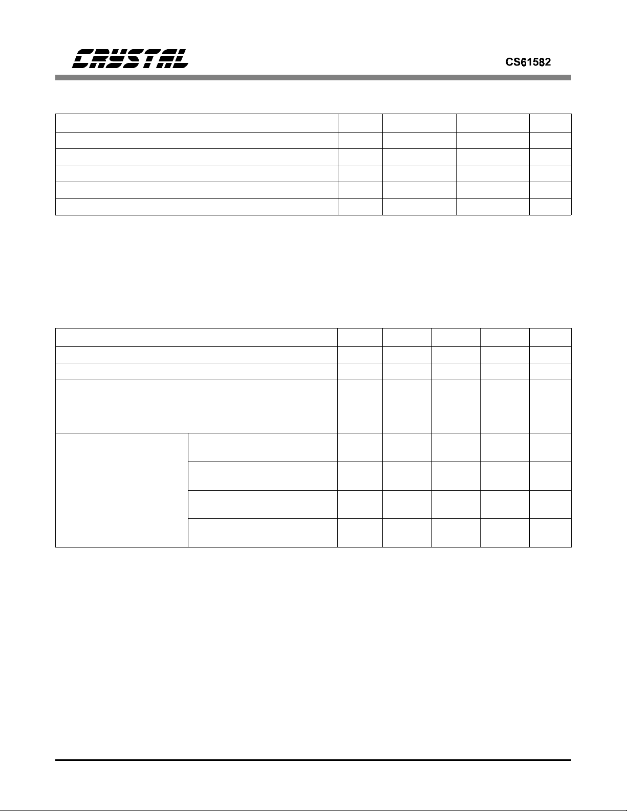
Figure 1. Signal Rise and Fall Characteristics
t
pwl1
t
su1
90% 90%
10% 10%
t
pw1
t
pwh1
t
h1
RCLK
(CLKE =0)
Figure 2. Recovered Clock and Data Sw itching Characterist ics
t
pw2
t
pwh2
TCLK
t
su2
t
h2
TPOS
TNEG
Figure 3. Transmit Clock and Data Switching Characteristics
DS224PP1 7
Page 8
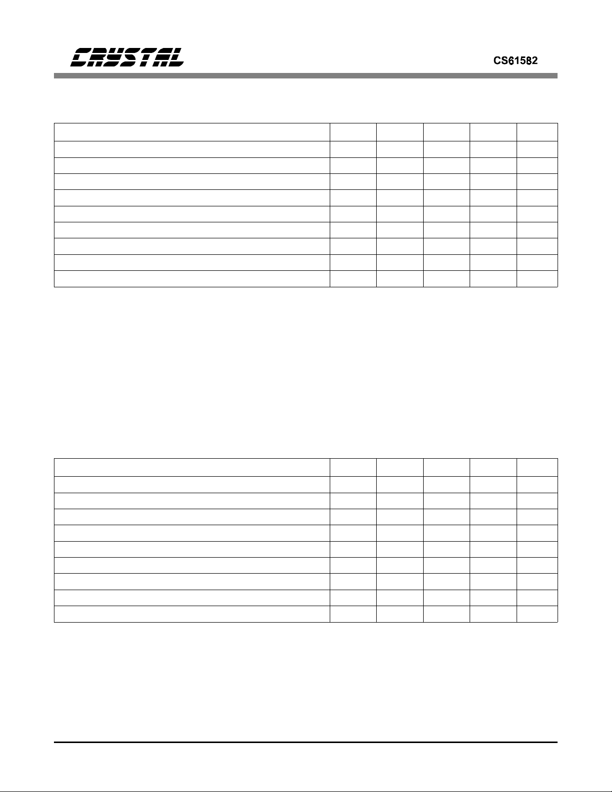
SWITCHING CHARACTERISTICS - JTAG
TV+, RV+ = nominal ±0.3V; Inputs: Logic 0 = 0V, Logic 1 = RV+) (See Figure 4)
Parameter S ymbol Min Typ Max Units
(TA = - 40 ° to 85 ° C;
Cycle Time t
J-TMS/J-TDI to J-TCK rising setup time t
J-TCK rising to J-TMS/J-TDI hold time t
J-TCK falling to J-TDO valid t
t
cyc
J-TCK
t
su
t
h
J-TMS
J-TDI
J-TDO
cyc
su
dv
200 - - ns
50 - - ns
h
50 - - ns
- - 50 ns
t
dv
Figure 4. JAG Switching Characte ristics
8 DS224PP1
Page 9

OVERVIEW
The CS61582 is a dual line interface optimized
for highly-integrated T1/E1 asynchronous or
synchronous multiplexer applications such as
SONET or SDH. One board design can support
all T1/E1 short-haul modes by only changing
component values in the receive and transmit
paths (if REFCLK and TCLK are externally t ied
together).
The line receiver contains all the necessary clock
and data recovery circuits.
The jitter attenuator meets AT&T 62411 requirements when using a 1X or 8X reference clock
supplied by either a crystal oscillator or external
reference at the REFCLK input pin.
TRANSMITTER
All control of the device is achieved via external
pins, eliminating the need for microprocessor
support. The following pin control options are
available on a per channel basis: line length selection, transmit all ones, local loopback, and
remote loopback.
The line driver generates waveforms compatible
with E1 (CCITT G.703), T1 short haul (DSX-1)
and T1 FCC Part 68 Option A (DS1). A single
transformer turns ratio is used for all waveform
types. The driver internally matches the impedance of the load, providing excellent return loss
to insure superior T1/E1 pulse quality. An additional benefit of the internal impedance matching
is a 50 percent reduction in power consumption
compared to implementing return loss using external resistors that causes the transmitter to
drive the equivalent of two line loads.
The transmitter accepts data from a T1 or E1
system and outputs pulses of appropriate shape
to the line. The transmit clock (TCLK) and
transmit data (TPOS and TNEG) are supplied
synchronously. Data is sampled on the falling
edge of the TCLK input.
The configuration pins CON[2:0] control transmitted pulse shapes, transmitter source
impedance, and receiver slicing level as shown in
Table 1. Typical output pulses are shown in Figures
5 and 6. These pulse shapes are fully pre-defined
by circuitry in the CS61582, and are fully compliant with appropriate standards when used with our
application guidelines in standard installations.
Both channels must be operated at the same line rate
(both T1 or both E1).
Note that the pulse width for Part 68 Option A
(324 ns) is narrower than the optimal pulse
width for DSX-1 (350 ns). The CS61582 auto-
C
C
C
Transmit Pulse
O
O
O
Width at 50%
N
N
N
2
1
0
000001244 ns (50%)
0 1 0 324 ns ( 50%) DS1: FCC Part 68 Option A (0 dB) 65%
0 1 1 350 ns ( 54%) DSX-1: 0-133 ft. / or DS1 FCC Part 68 Option A with undershoot 65%
1 0 0 350 ns ( 54%) DSX-1: 133-266 ft. 65%
1 0 1 350 ns ( 54%) DSX-1: 266-399 ft. 65%
1 1 0 350 ns ( 54%) DSX-1: 399-533 ft. 65%
1 1 1 350 ns ( 54%) DSX-1: 533-655 ft. 65%
DS224PP1 9
Amplitude
244 ns (50%)
Transmit Pulse Shape
E1: square, 2.37 Volts into 75 Ω
E1: square, 3.00 Volts into 120 Ω
Table 1. Configuration Selection
Receiver
Slicing
Level
50%
50%
Page 10
NORMALIZED
AMPLITUDE
1.0
ANSI T1.102
SPECIFICATIO N
0.5
0
CS61582
OUTPUT
PULSE SHAPE
-0.5
0 250 750 1000
500
TIME (nanoseconds)
Figure 5. Typical Pulse Shape at DSX-1 Cross Connect
matically adjusts the pulse width based on the
configuration selection.
120
110
100
-10
-20
Percent of
nominal
peak
voltage
90
80
50
10
0
269 ns
244 ns
194 ns
G.703
SPECIFICATION
Nominal Pulse
219 ns
488 ns
The transmitter impedance changes with the line
length options in order to match the load imped-
ance (75Ω for E1 coax, 100Ω for T1, 120Ω for
E1 shielded twisted pair), providing a minimum
of 14 dB return loss for T1 and E1 frequencies
during the transmission of both marks and
spaces. This improves signal quality by minimizing reflections from the transmitter. Impedance
matching also reduces load power consumption
by a factor of two when compared to the return
loss achieved by using external resistors.
The CS61582 driver will automatically detect an
inactive TLCK input (i.e., no valid data is being
clocked to the driver). When this condition is detected, the driver is forced low (except during
remote loopback) to output spaces and prevent
TTIP and TRING from entering a constant transmit-mark state.
When the transmit configuration established by
CON[2:0], TAOS, or LLOOP changes state, the
transmitter stabilizes within 22 TCLK bit periods. The transmitter takes longer to stabilize
when RLOOP1 or RLOOP2 is selected because
Figure 6. Pulse Mask at the 2048 kbps Interface
the timing circuitry must adjust to the new frequency from RCLK.
When the transmitter transformer secondaries are
shorted through a 0.5 ohm resistor, the transmitter will output a maximum of 50 mA-rms, as
required by European specification BS6450.
RECEIVER
The receiver extracts data and clock from the
T1/E1 signal on the line interface and outputs
clock and synchronized data to the system. The
signal is detected differentially across the receive
transformer and can be recovered over the entire
range of short haul cable lengths. The transmit
and receive transfomer specifications are identical
and are presented in the Applications section.
As shown in Table 1, the receiver slicing level is
set at 65% for DS1/DSX-1 short-haul and at
50% for all other applications.
10 DS224PP1
Page 11
The clock recovery circuit is a second-order
phase locked loop that can tolerate up to 0.4 UI
of jitter from 10 kHz to 100 kHz without generating errors (Figure 7). The clock and data
recovery circuit is tolerant of long strings of consecutive zeros and will successfully recover a
1-in-175 jitter-free line input signal.
CS61582
Performance
PEAK-TO-PEAK
JITTER
(unit intervals)
300
138
100
AT&T 62411
28
10
(1990 Version)
0
10
20
30
b) Maximum
40
Atte n ua tion
Attenuation in dB
Lim it
50
60
1 10 100 1 k 10 k
a) Minimum Attenuation Limit
62411 (1990 Version)
Requirements
CS61582 P erformance
Frequency in Hz
Figure 8. Typical Jitter Transfer Function
1
.4
.1
1 100 100k
10
JITTER FREQUENCY (Hz)
300
700
1k
10k
Figure 7. Minimum Input Jitter Tolerance of Receiver
Recovered data at RPOS and RNEG is stable
and may be sampled using the recovered clock
RCLK. The CLKE input determines the clock
polarity where the output data is stable and valid
as shown in Table 2. When CLKE is low, RPOS
and RNEG are valid on the rising edge of
RCLK. When CLKE is high, RPOS and RNEG
are valid on the falling edge of RCLK.
CLKE DATA CLOCK Clock Edge
for Valid Data
LOW RPOS
RNEG
HIGH RPOS
RNEG
RCLK
RCLK
RCLK
RCLK
Rising
Rising
Falling
Falling
The attenuator consists of a 64-bit FIFO, a narrow-band monolithic PLL, and control logic.
Signal jitter is absorbed in the FIFO which is designed to neither overflow nor underflow. If
overflow or underflow is imminent, the jitter
transfer function is altered to insure that no biterrors occur. Under this condition, jitter gain
may occur and jitter should be attenuated externally in a frame buffer. The jitter attenuator will
typically tolerate 43 UIs before the overflow/underflow mechanism occurs. If the jitter
attenuator has not had time to "lock" to the average incoming frequency (e.g., following a device
reset) the attenuator will tolerate a minimum of
22 UIs before the overflow/underflow mechanism occurs. The attenuator can accept a
transmit clock with gaps ≤ 28 UIs and a transmit
clock burst rate of ≤ 8 MHz.
When a loss of signal occurs, the last recovered
frequency is not held and the output frequency becomes the frequency of the reference clock.
Table 2. Re covere d Data /Cloc k Optio ns
REFERENCE CLOCK
JITTER ATTENUATOR
The jitter attenuator is located in the transmit
path of each channel to remove gapped clock jitter on TCLK. Figure 8 illustrates the typical
jitter attenuation curve.
DS224PP1 11
The CS61582 requires a reference clock with a
minimum accuracy of ±100 ppm for T1 and E1
applications. This clock can be either a 1X clock
(i.e., 1.544 MHz or 2.048 MHz), or can be a 8X
clock (i.e., 12.352 MHz or 16.384 MHz) as se-
Page 12

lected by the 1XCLK pin. In systems with a jittered transmit clock, the reference clock should
not be tied to the transmit clock and a separate
external oscillator should drive the reference
clock input. Any jitter present on the reference
clock will not be filtered by the jitter attenuator.
POWER-UP RESET
On power-up, the device is held in a static state
until the power supply achieves approximately
60% of the power supply voltage. When this
threshold is crossed, the device waits another 10
ms to allow the power supply to reach operating
voltage and then calibrates the transmit and receive circuitry. This initial calibration takes less
than 20 ms but can occur only if REFCLK and
TCLK are present. The power-up reset performs
the same functions as the RESET pin.
connected the transmitter output pins of another
channel or device.
Loss of Signal
The loss of signal (LOS) indication is detected
by the receiver and reported by setting the LOS
pin high. Loss of signal is indicated when
175±15 consecutive zeros are received. The LOS
condition is exited according to the ANSI
T1.231-1993 criteria that requires 12.5% ones
density over 175±75 bit periods with no more
than 100 consecutive zeros. Note that bit errors
may occur at RPOS and RNEG prior to the LOS
indication if the analog input level falls below
the receiver sensitivity.
The LOS pin is set high when the device is reset
or in power-up and returns low when data is recovered by the receiver.
LINE CONTROL AND MONITORING
Line control and monitoring of the CS61582 is
achieved using the control pins. The controls and
indications available on the CS61582 are detailed below.
Device Performance Monitor
To aid in the early detection and easy isolation
of non-functioning links, the CS61582 is capable
of monitoring the transmit driver performance
and report when the driver is no longer operational. The driver performance monitor consists
of an activity detector that monitors t he transmitted signal when MTIP is connected to TTIP and
MRING is connected to TRING. The DPM output will go high when the differential inputs
MTIP and MRING are inactive for 512±2
REFCLK periods. The DPM output returns low
when the monitor senses a minimum 12.5% ones
density signal over 175±75 bit periods with no
more than 100 consecutive zeros. To increase the
reliability of the performance monitor, it is suggested that the monitor inputs of one channel be
Transmit All Ones
Transmit all ones is selected by setting the
TAOS pin high. Selecting TAOS causes continuous ones to be transmitted to the line interface
on TTIP and TRING at the frequency of
REFCLK. In this mode, the transmit data inputs
TPOS and TNEG are ignored. A TAOS request
overrides the data transmitted to the line interface during local and remote loopbacks.
Local Loopback
A local loopback is selected by setting the
LLOOP pin high. Selecting LLOOP causes the
TCLK, TPOS, and TNEG inputs to be looped
back through the jitter attenuator to the RCLK,
RPOS, and RNEG outputs. Data received at the
line interface is ignored, but data at TPOS and
TNEG continues to be transmitted to the line interface at TTIP and TRING.
A TAOS request overrides the data transmitted to
the line interface during local loopback. Note
that simultaneous selection of local and remote
loopback modes is not valid.
12 DS224PP1
Page 13

Remote Loopback
A remote loopback is selected by setting the
RLOOP pin high. Selecting RLOOP causes the
data received from the line interface at RTIP and
RRING to be looped back through the jitter attenuator and retransmitted on TTIP and TRING.
Data transmitted at TPOS and TNEG is ignored,
but data recovered from RTIP and RRING continues to be transmitted on RPOS and RNEG.
Remote loopback is functional if TCLK is absent. A TAOS request overrides the data
transmitted to the line interface during a remote
loopback. Note that simultaneous selection of local and remote loopback modes is not valid.
and receive circuitry is calibrated if REFCLK
and TCLK are present.
JTAG BOUNDARY SCAN
Board testing is supported through JTAG boundary scan. Using boundary scan, the integrity of
the digital paths between devices on a circuit
board can be verified. This verification is supported by the ability to externally set the signals
on the digital output pins of the CS61582, and to
externally read the signals present on the input
pins of the CS61582. Additionally, the manufacturer ID, part number and revision of the
CS61582 can be read during board test using
JTAG boundary scan.
Reset Pin
The CS61582 is continuously calibrated during
operation to insure the performance of the device
over power supply and temperature. This continuous calibration function eliminates the need
to reset the line interface during operation.
A device reset may be selected by setting the
RESET pin high for a minimum of 200 ns. The
reset function initiates on the falling edge of RESET and requires less than 20 ms to complete.
The control logic is initialized and the transmit
Digital output pins Digital i nput pins
parallel latched
output
Boundary Sc an D at a Reg i st er
Device ID Data Register
J-TDI
Bypass Data Register
As shown in Figure 9, the JTAG hardware consists of data and instruction registers plus a Test
Access Port (TAP ) controller. Control of the TAP
is achieved through signals applied to the Test
Mode Select (J-TMS) and Test Clock ( J-TCK)
input pins. Data is shifted into the registers via
the Test Data Input (J-TDI) pin, and shifted out
of the registers via the Test Data Output (J-TDO)
pin. Both J-TDI and J-TDO are clocked at a rate
determined by J-TCK. The Instruction register
defines which data register is accessed in the
JTAG Block
MUX
J-TDO
J-TCK
J-TMS
DS224PP1 13
Instructi on (shift) Register
parallel latched
output
TAP
Controller
Figure 9. Block Dia gram of JTAG Circuitry
Page 14

shift operation. Note that if J-TDI is floating,
an internal pull-up resistor forces the pin high.
JTAG Data Registers (DR)
The test data registers are the Boundary-Scan
Register (BSR), the Device Identification Register (DIR), and the Bypass Register (BR).
BSR bits Pin Name Pad Type
0-2 LOS1 bi-directional
3-5 TNEG1 bi-directional
6 TPOS1 input
7 TCLK1 input
8-9 RNEG1 output
10-11 RPOS1 output
12-13 RCLK1 output
14-16 DP M1 bi-directional
17-19 RLOOP1 bi-directional
20 LLOOP2 input
21-23 LLOOP1 bi-direct ional
24-26 TAOS1 bi-direc tional
27-29 TAOS2 bi-direc tional
30-32 CO N01 bi-directional
33-35 CO N02 bi-directional
36-38 CON11 bi-directional
39-41 CO N12 bi-directional
42-44 CO N21 bi-directional
45 CON22 input
46-48 DP M2 bi-directional
49-50 RCLK2 output
51-52 RPOS2 output
53-54 RNEG2 output
55 TCLK2 input
56 TPOS2 input
57-59 TNEG 2 bi-directional
60-62 LOS2 bi-directional
63 CLKE input
64 RLOOP2 input
1. Configure pad as an input.
2. Configure pad as an output.
Table 3. Boundary Scan Register
2
1
2
1
1
1
1
1
1
1
1
1
2
1
2
Boundary Scan Register: The BSR is connected
in parallel to all the digital I/O pins, and provides the mechanism for applying/reading test
patterns to/from the board traces. The BSR is 65
bits long and is initialized and read using the instruction SAMPLE/PRELOAD. The bit ordering
for the BSR is the same as the top-view package
pin out, beginning with the LOS1 pin and moving counter-clockwise to end with the RLOOP2
pin as shown in Table 3.
The input pins require one bit in the BSR and
only one J-TCK cycle is required to load test
data for each input pin.
The output pins have two bits in the BSR to define output high, output low, or high impedance.
The first bit (shifted in first) selects between an
output-enabled state (bit set to 1) or high-impedance state (bit set to 0). The second bit shifted in
contains the test data that may be output on the
pin. Therefore, two J-TCK cycles are required to
load test data for each output pin.
The bi-directional pins have three bits in the
BSR to define input, output high, output low, or
high impedance. The first bit shifted into the
BSR configures the output driver as high-impedance (bit set to 0) or active (bit set to 1). The
second bit shifted into the BSR sets the output
value when the first bit is 1. The third bit captures the value of the pin. This pin may have its
value set externally as an input (if the first bit is
0) or set internally as an output (if the first bit is
1). To configure a pad as an input, the J-TDI
pattern is 0X0. To configure a pad as an output,
the J-TDI pattern is 1X1. Therefore, three J-TCK
cycles are required to load test data for each bidirectional pin.
Device Identification Register: The DIR provides
the manufacturer, part number, and version of the
CS61582. This information can be used to verify
that the proper version or revision number has
been used in the system under test. The DIR is 32
bits long and is partitioned as shown in figure 10.
14 DS224PP1
Page 15

MSB LSB
31 28 27 12 11 1 0
00000000000000000011000011001001
(4 bits) (16 bits) (11 bits)
BIT #(s) FUNCTION Total Bits
31-28 Version number 4
27-12 Part Number 16
11- 1 Manufacturer Number 11
0 Constant Logic ’1’ 1
Figure 10. Device Identification Register
Data from the DIR is shifted out to J-TDO LSB
first.
Bypass Register: The Bypass register consists of
a single bit, and provides a serial path between
J-TDI and J-TDO, bypassing the BSR. This allows bypassing specific devices during certain
board-level tests. This also reduces test access
times by reducing the total number of shifts required from J-TDI to J-TDO.
SAMPLE/PRELOAD Instruction: The SAMPLE/PRELOAD instructions allows scanning of
the boundary-scan register without interfering
with the operation of the CS61582. This instruction connects the BSR to the J-TDI and J-TDO
pins. The normal path between the CS61582
logic and its I/O pins is maintained. The signals
on the I/O pins are loaded into the BSR. Additionally, this instruction can be used to latch
values into the digital output pins.
IDCODE Instruction: The IDCODE instruction
connects the device identification register to the
J-TDO pin. The IDCODE instruction is forced
into the instruction register during the TestLogic-Reset controller state.The default
instruction is IDCODE after a device reset.
BYPASS Instruction: The BYPASS instruction
connects the minimum length bypass register between the J-TDI and J-TDO pins and allows data
to be shifted in the Shift-DR controll er state.
JTAG Instructions and Instruction Register (IR)
The instruction register (2 bits) allows the instruction to be shifted into the JTAG circuit. The
instruction selects the test to be performed or the
data register to be accessed or both. The valid
instructions are shifted in LS B first and are listed
below:
IR CODE INSTRUCTION
00 EX TEST
01 SA MPLE/PRELOAD
10 IDCODE
11 BYPASS
EXTEST Instruction: The EXTEST instruction
allows testing of off-chip circuitry and boardlevel interconnect. EXTEST connects the BSR to
the J-TDI and J-TDO pins. The normal path between the CS61582 logic and I/O pins is broken.
The signals on the output pins are loaded from
the BSR and the signals on the input pins are
loaded into the BSR.
Internal Testing Considerations
Note that the INTEST instruction is not supported because of the difficulty in performing
significant internal tests using JTAG.
The one test that could be easily performed using an arbitrary clock rate on TCLK and
REFCLK is a local loopback with jitter attenuator disabled. However, this test provides limited
fault coverage and is only useful in determining
if the device had been catastrophically destroyed.
Alternatively, catastrophic destruction of the device and/or surrounding board traces can be
detected using EXTEST. Therefore, the INTEST
instruction provides limited testing capability
and was not included in the CS61582.
JTAG TAP Controller
Figure 11 shows the state diagram for the TAP
state machine. A description of each state follows. Note that the figure contains two main
branches to access either the data or instruction
DS224PP1 15
Page 16

registers. The value shown next to each state
transition in this figure is the value present at
J-TMS at each rising edge of J-TCK.
Test-Logic-Reset State
In this state, the test logic is disabled to continue
normal operation of the device. During initialization, the CS61582 initializes the instruction
register with the IDCODE instruction.
Select-DR-Scan State
This is a temporary controller state. The test
data register selected by the current instruction
retains its previous state. If J-TMS is held low
and a rising edge is applied to J-TCK when in
this state, the controller moves into t he CaptureDR state and a scan sequence for the selected
test data register is initiated. If J-TMS is held
high and a rising edge applied to J-TCK, the
controller moves to the Select-IR-Scan state.
Regardless of the original state of the cont roller,
the controller enters the Test-Logic-Reset state
when the J-TMS input is held high for at least
five rising edges of J-TCK. The controller remains in this state while J-TMS is high. The
CS61582 processor automatically enters this
state at power-up.
Run-Test/Idle State
This is a controller state between scan operations. Once in this state, the controller remains
in the state as long as J-TMS is held low. The
instruction register and all test data registers retain their previous state. When J-TMS is high
and a rising edge is applied to J-TCK, the controller moves to the Select-DR state.
Test-Logic-Reset
1
0
0
Run-Test/Idle
1
Select-DR-Scan
1
Capture-DR
Pause-DR
0
Update-DR
10
0
0
Shift-DR
1
Exit1-DR
0
1
Exit2-DR
1
The instruction does not change in this state.
Capture-DR State
In this state, the Boundary Scan Register captures input pin data if the current instruction is
EXTEST or SAMPLE/PRELOAD. The other
test data registers, which do not have parallel input, are not changed.
The instruction does not change in this state.
When the TAP controller is in this state and a
rising edge is applied to J-TCK, the controller
enters the Exit1-DR state if J-TMS is high or the
Shift-DR state if J-T MS is low.
1
0
1
0
Select-IR-Scan
1
0
10
0
Capture-IR
0
Shift- IR
1
Exit1-IR
0
Pause-IR
1
Exit2-IR
1
Update-IR
1
0
1
0
Figure 11. TAP Controller State Diagram
16 DS224PP1
Page 17

Shift-DR State
Exit2-DR State
In this controller state, the test data register connected between J-TDI and J-TDO as a result of
the current instruction shifts data on stage toward its serial output on each rising edge of
J-TCK.
The instruction does not change in this state.
When the TAP controller is in this state and a
rising edge is applied to J-TCK, the controller
enters the Exit1-DR state if J-TMS is high or remains in the Shift-DR state if J-TMS is low.
Exit1-DR State
This is a temporary state. While in t his state, if
J-TMS is held high, a rising edge applied to JTCK causes the controller to enter the
Update-DR state, which terminates the scanning
process. If J-TMS is held low and a rising edge
is applied to J-TCK, the controller enters the
Pause-DR state.
The test data register selected by the current instruction retains its previous value during this
state. The instruction does not change in this
state.
Pause-DR State
The pause state allows the test controller to temporarily halt the shifting of data through the test
data regist er in the serial path between J-TDI and
J-TDO. For example, this state could be used to
allow the tester to reload its pin memory from
disk during application of a long test sequence.
The test data register selected by the current instruction retains its previous value during this
state. The instruction does not change in this
state.
The controller remains in this state as long as
J-TMS is low. When J-TMS goes high and a
rising edge is applied to J-TCK, the controller
moves to the Exit2-DR state.
This is a temporary state. While in t his state, if
J-TMS is held high, a rising edge applied to JTCK causes the controller to enter the
Update-DR state, which terminates the scanning
process. If J-TMS is held low and a rising edge
is applied to J-TCK, the controller enters the
Shift-DR state.
The test data register selected by the current instruction retains its previous value during this
state. The instruction does not change in this
state.
Update-DR State
The Boundary Scan Register is provided with a
latched parallel output to prevent changes while
data is shifted in response to the EXTEST and
SAMPLE/PRELOAD instructions. When the
TAP controller is in this state and the Boundary
Scan Register is selected, data is latched into the
parallel output of this register from the shift-register path on the falling edge of J-TCK. The
data held at the latched parallel output changes
only in this state.
All shift-register stages in the test data register
selected by the current instruction retains their
previous value during this state. The instructions
does not change in this state.
Select-IR-Scan State
This is a temporary controller state. The test
data register selected by the current instruction
retains its previous state. If J-TMS is held low
and a rising edge is applied to J-TCK when in
this state, the controller moves into t he CaptureIR state, and a scan sequence for the instruction
register is initiated. If J-TMS is held high and a
rising edge is applied to J-TCK, the controller
moves to the Test-Logic-Reset state. The instruction does not change in this state.
DS224PP1 17
Page 18

Capture-IR State
Pause-IR State
In this controller state, the shift register contained in the instruction register loads a fixed
value of "01" on the rising edge of J-TCK. This
supports fault-isolation of the board-level serial
test data path.
Data registers selected by the current instruction
retain their value during this state. The instructions does not change in this state.
When the controller is in this state and a rising
edge is applied to J-TCK, the controller enters
the Exit1-IR state if J-TMS is held high, or the
Shift-IR state if J-TMS is held low.
Shift-IR State
In this state, the shift register contained in the
instruction register is connected between J-TDI
and J-TDO and shifts data one stage towards its
serial output on each rising edge of J-TCK.
The test data register selected by the current instruction retains its previous value during this
state. The instruction does not change in this
state.
When the controller is in this state and a rising
edge is applied to J-TCK, the controller enters
the Exit1-IR state if J-TMS is held high, or remains in the Shift-IR state if J-TMS is held low.
Exit1-IR State
This is a temporary state. While in t his state, if
J-TMS is held high, a rising edge applied to JTCK causes the controller to enter the Updat e-IR
state, which terminates the scanning process. If
J-TMS is held low and a rising edge is applied
to J-TCK, the controller enters the Pause-IR
state.
The test data register selected by the current instruction retains its previous value during this state.
The instruction does not change in this state.
The pause state allows the test controller to temporarily halt the shifting of data through the
instruction register.
The test data register selected by the current instruction retains its previous value during this
state. The instruction does not change in this
state.
The controller remains in this state as long as
J-TMS is low. When J-TMS goes high and a
rising edge is applied to J-TCK, the controller
moves to the Exit2-IR state.
Exit2-IR State
This is a temporary state. While in t his state, if
J-TMS is held high, a rising edge applied to JTCK causes the controller to enter the Updat e-IR
state, which terminates the scanning process. If
J-TMS is held low and a rising edge is applied
to J-TCK, the controller enters the Shift-IR state.
The test data register selected by the current instruction retains its previous value during this
state. The instruction does not change in this
state.
Update-IR State
The instruction shifted into the instruction register is latched into the parallel output from the
shift-register path on the falling edge of J-TCK.
When the new instruction has been latched, it
becomes the current instruction.
Test data registers selected by the current instruction retain their previous value.
JTAG Application Examples
Figures 12 and 13 illustrate examples of updating the instruction and data registers during
JTAG operation.
18 DS224PP1
Page 19

TCK
TMS
Controller state
TDI
Parallel Input to IR
IR shift-register
Test-Logic-Reset
Shift-IR
Exit1-IR
Select-DR-Scan
Select-IR-Scan
Capture-IR
Run-Test/Idle
Pouse-IR
Exit2-IR
Shift-IR
Exit1-IR
Update-IR
Run-Test/Idle
Parallel out put of IR
Parallel I n put t o TDR
Parallel output of TDR
TDR shift-register
Register selecte d
TDO enable
TDO
IDCODE New Instruction
Old data
Instruction register
Inactive ActiveInactive Inactive
Act
= Don't care or undef i ned
Figure 12. JTAG Instruction Register Update
DS224PP1 19
Page 20

TCK
TMS
Controller state
TDI
Parallel Input to IR
IR shift- regi s te r
Shift-DR
Exit1-DR
Run-Test/Idle
Select-DR-Scan
Capture-DR
Pouse-DR
Exit2-DR
Shift-DR
Exit1-DR
Update-DR
Run-Test/Idle
Select-DR-Scan
Select-IR-Scan
Test-Logic-Reset
Parallel output of IR
Parallel Input to TDR
TDR shift-register
Parallel output of TDR
Register Selected
TDO enable
TDO
Inactive ActiveInactive InactiveActive
= Don't care or undefined
Figure 13. JTAG Data Register Update
Old data
IDCODEInstruction
New data
Test data register
20 DS224PP1
Page 21

PIN DESCRIPTIONS
DGND1
CON01
TAOS2
TAOS1
LLOOP2
LLOOP1
RLOOP1
DPM1
RCLK1
RPOS1
RNEG1
TCLK1
TPOS1
TNEG1
LOS1
J-TDO
DGND2
J-TDI
TTIP1
TV+1
TGND1
TRING1
MRING1
MTIP1
RTIP1
RRING1
RV+1
RGND1
AGND1
BGREF
AGND2
AV+
64 62 60 58 56 54 52 50
1
2
4
6
8
10
12
14
16
18 20 22 24 26 28 30 32
CS6 1582
64-P in TQ FP
Top View
48
46
44
42
40
38
36
34
DV+
DGND3
CON02
CON11
CON12
CON21
CON22
DPM2
RCLK2
RPOS2
RNEG2
TCLK2
TPOS2
TNEG2
LOS2
CLKE
J-TCK
J-TMS
TTIP2
TV+2
TGND2
TRING2
MRING2
MTIP2
RTIP2
RRING2
RV+2
RGND2
1XCLK
RLOOP2
REFCLK
RESET
DS224PP1 21
Page 22

Power Supplies
AGND1, AGND2 : Analog Ground (Pins 21, 23)
Analog supply ground pins.
AV+ : Analog Power Supply (Pin 24)
Analog supply pin for the internal bandgap reference and timing generation circuits.
BGREF : Bandgap Reference (Pin 22)
This pin is used by the internal bandgap reference and must be connected to ground
by a 4.99kΩ ± 1% resistor to provide an internal current reference.
DGND1, DGND2, DGND3 : Digital Ground (Pins 57, 9, 55)
Power supply ground pins for the digital circuitry of both channels.
DV+ : Power Supply (Pin 56)
Power supply pin for the digital circuitry of both channels.
RGND1, RGND2 : Receiver Ground (Pins 20, 29)
Power supply ground pins for the receiver circuitry.
RV+1, RV+2 : Receiver Power Supply (Pins 19, 30)
Power supply pins for the analog receiver circuitry.
TGND1, TGND2 : Transmit Ground (Pins 13, 36)
Power supply ground pins for the transmitter circuitry.
TV+1, TV+2 : Transmit Power Supply (Pins 12, 37)
Power supply pins for the analog transmitter circuitry.
T1/E1 Data
RCLK1, RCLK2 : Receive Clock (Pins 1, 48)
RPOS1, RPOS2 : Receive Positive Data (Pins 2, 47)
RNEG1, RNEG2 : Receive Negative Data (Pins 3, 46)
The receiver recovered clock and NRZ digital data from RTIP and RRING is output on these
pins. The CLKE pin determines the clock edge on which RPOS and RNEG are stable and valid
as shown in Table 2. A positive pulse (with respect to ground) received on RTIP generates a
logic 1 on RPOS, and a positive pulse received on RRING generates a logic 1 on RNEG.
RTIP1, RTIP2 : Receive Tip (Pins 17, 32)
RRING1, RRING2 : Receive Ring (Pins 18, 31)
The receive AMI signal from the line interface is input on these pins. The recovered clock and
data are output on RCLK, RPOS, and RNEG.
TTIP1, TTIP2 : Transmit Tip (Pins 11, 38)
TRING1, TRING2 : Transmit Ring (Pins 14, 35)
The transmit AMI signal to the line interface is output on these pins. The transmit clock and
data are input from TCLK, TPOS, and TNEG.
22 DS224PP1
Page 23

TCLK1, TCLK2 : Transmit Clock (Pins 4, 45)
TPOS1, TPOS2 : Transmit Positive Data (Pins 5, 44)
TNEG1, TNEG2 : Transmit Negative Data (Pins 6, 43)
The transmit clock and data are input on these pins. The signal is driven to the line at TTIP and
TRING. Data on TPOS and TNEG are sampled on the falling edge of TCLK. An input on
TPOS causes a positive pulse to be transmitted at TTIP and TRING, while an input on TNEG
input causes a negative pulse to be transmitted at TTIP and TRING.
Oscillator
1XCLK : One-times Clock Frequency Select (Pin 28)
When 1XCLK is set high, REFCLK must be a 1X clock (i.e., 1.544 MHz for T1 applications or
2.048 MHz for E1 applications). When 1XCLK is set low, REFCLK must be an 8X clock (i.e.,
12.352 MHz for T1 applications or 16.384 MHz for E1 applications).
REFCLK : External Reference Clock Input (Pin 26)
Input reference clock for the receive and jitter attenuator circuits. When 1XCLK is set high,
REFCLK must be a 1X clock (i.e., 1.544 MHz ±100 ppm for T1 applications or 2.048 MHz
±100 ppm for E1 applications). When 1XCLK is set low, REFCLK must be an 8X clock (i.e.,
12.352 MHz ±100 ppm for T1 applications or 16.384 MHz ±100 ppm for E1 applications). The
REFCLK input also determines the transmission rate when TAOS is asserted.
Control
CLKE : Clock Edge (Pin 41)
Controls the polarity of the recovered clock RCLK. When CLKE is high, RPOS and RNEG are
valid on the falling edge of RCLK. When CLKE is low, RPOS and RNEG are valid on the
rising edge of RCLK.
CON01, CON11, CON21 : Configuration for Channel 1 (Pins 58, 53, 51)
CON02, CON12, CON22 : Configuration for Channel 2 (Pins 54, 52, 50)
These pins configure the transmitter (pulse shape, pulse width, pulse amplitude, and driver
impedance) and receiver (slicing level). The CONx1 pins control channel 1 and the CONx2
pins control channel 2. Both channels must be configured to operate at the same data rate on
the line interface (both T1 or both E1).
LLOOP1, LLOOP2 : Local Loopback (Pins 62, 61)
A local loopback is enabled when LLOOP is high. During local loopback, the TCLK, TPOS,
and TNEG inputs are looped back through the jitter attenuator to the RCLK, RPOS, and RNEG
outputs. The data at TPOS and TNEG continues to be transmitted to the line interface unless
overridden by a TAOS request. The inputs at RTIP and RRING are ignored.
RESET : Reset (Pin 25)
A device reset is selected by setting the RESET pin high for a minimum of 200 ns. The reset
function initiates on the falling edge of RESET and requires less than 20 ms to complete. The
control logic is initialized and LOS is set high.
DS224PP1 23
Page 24

RLOOP1, RLOOP2 : Remote Loopback (Pins 63, 27)
A remote loopback is selected when RLOOP is high. The data received from the line interface
at RTIP and RRING is looped back through the jitter attenuator and retransmitted on TTIP and
TRING. Data recovered from RTIP and RRING continues to be transmitted on RPOS and
RNEG. Data input on TPOS and TNEG is ignored. A TAOS request overrides the data
transmitted at TTIP and TRING.
TAOS1, TAOS2 : Transmit All Ones Select (Pins 60, 59)
Setting TAOS high causes continuous ones to be transmitted at the line interface on TTIP and
TRING at the frequency determined by REFCLK.
Status
DPM1, DPM2 : Driver Performance Monitor Alarm (Pins 64, 49)
The DPM alarm indication goes high when differential inputs MTIP and MRING are inactive
for 512 ± 2 REFCLK periods. The DPM alarm indication returns low when MTIP and MRING
detect a minimum 12.5% ones density signal over 175 ± 75 bit periods with no more than 100
consecutive zeros.
MTIP1, MTIP2 : Monitor Tip (Pins 16, 33)
MRING1, MRING2 : Monitor Ring (Pins 15, 34)
The MTIP and MRING inputs may be connected to TTIP and TRING, to detect an inactive
transmit driver. The MTIP and MRING inputs are differential and may be connected to either
transmitter output. To increase the reliability of the performance monitor, it is suggested that the
monitor inputs of one channel be connected the transmitter output pins of another channel or
device.
LOS1, LOS2 : Loss of Signal (Pins 7, 42)
The LOS indication goes high when 175 ± 15 consecutive zeros are received on the line
interface. The LOS indication returns low when a minimum 12.5% ones density signal over
175 ± 75 bit periods with no more than 100 consecutive zeros is received.
Test
J-TCK : JTAG Test Clock (Pin 40)
Data on pins J-TDI and J-TDO is valid on the rising edge of J-TCK. When J-TCK is stopped
low, all JTAG registers remain unchanged.
J-TMS : JTAG Test Mode Select (Pin 39)
An active high signal on J-TMS enables the JTAG serial port. This pin has an internal pull-up
resistor.
J-TDI : JTAG Test Data In (Pin 10)
JTAG data is shifted into the device on this pin. This pin has an internal pull-up resistor. Data
must be stable on the rising edge of J-TCK.
J-TDO : JTAG Test Data Out (Pin 8)
JTAG data is shifted out of the device on this pin. This pin is active only when JTAG testing is
in progress. J-TDO will be updated on the falling edge of J-TCK.
24 DS224PP1
Page 25

PHYSICAL DIMENSIONS
E
E
1
64
1
D
D
1
64-Pin
TQFP
MILLIMETERS INCHES
DIM
A
A
B
C
D
D
E
E
e
L
∝∝
MIN
-
0.00
1
0.14
0.077
11.70
10.00
1
11.70
10.00
1
0.40
0.35
0° 12° 0° 12°
MAX
1.66
-
0.26
0.177
12.30
10.00
12.30
10.00
0.60
0.70
MIN
-
0.00
0.006
0.003
0.461
0.394
0.461
0.394
0.016
0.014
MAX
0.068
-
0.010
0.007
0.484
0.394
0.484
0.394
0.024
0.028
A
A
C
B
e
1
Terminal
Detail 1
∝∝
L
DS224PP1 25
Page 26

APPLICATIONS
Framer
Framer
3
3
2
2
REFCLK 1XCLK
Clock Generator
TCLK1
TPOS1
TNEG1
RCLK1
RPOS1
RNEG1
TCLK2
TPOS2
TNEG2
RCLK2
RPOS2
RNEG2
AV+ AGND1:2 BGREF TV+1 TGND1 RV+1 RGND1 DV+ DGND1:3
0.1 µF
V
+
CC
1 µF
RESET CLKE RLOOP[1:2]TAOS[1:2] LLOOP[1:2] DPM[1:2]MTIP[1:2] MRING[1:2]LOS[1:2]CON[0:2]2CON[0:2]1
2
R3
5k
Ω
Hardware Control
Channel 1
Channel 2
TV+2TGND2 RV+2RGND2
F 0.1 µF0.1 µF
0.1
µ
Power Supply
0.1 µF
+
22 µF
22 2 2
2
Figure A1. Typical Connection Diagram
TTIP1
TRING1
RTIP1
RRING1
TTIP2
TRING2
RTIP2
RRING2
0.01 µF
3
0.47µF
R1
0.47
R2
0.47µF
R3
0.47
R4
C1
µ
C2
µ
1:1.15
T1
transmit
T2
1:1.15
F
T3
T4
F
receive
1:1.15
transmit
1:1.15
receive
Data Rate (MHz) REFCLK Frequency (MHz)
1XCLK = 1 1XCLK = 0
1.544 1.544 12.352 100 38.3 220
2.048 2.048 16.384 75 28.7 470
Table A1. CS61582 External Components
Line Interface
Figure A1 illustrates a typical connection diagram
and Table A1 lists the external components that
are required in T1 and E1 applications.
In the transmit line interface circuitry, capacitors
C1 and C2 provide transmitter return loss. The
0.47 µF capacitor in series with the transformer
primary prevents output stage imbalances from
producing a DC current through the transformer
that might saturate the transformer and result in
an output level offset.
Cable (Ω)R1-R4 (
Ω
)
C1-C2 (pF)
120 45.3 220
In the receive line interface circuitry, resistors R1R4 provide receive impedance matching and
receiver return loss. The 0.47 µF capacitor to
ground provides the necessary differential input
voltage reference for the receiver.
Power Supply
As shown in Figure A1, the CS61582 operates
from a 5.0 Volt supply. Separate analog and digital power supply and ground pins provide internal
isolation. The TGND, RGND, and DGND ground
pins must not be more negative than AGND. It is
recommended that all of the supply pins be con-
26 DS224PP1
Page 27

nected together at the device. A 4.99kΩ ± 1% resistor must be connected from BGREF to ground
to provide an internal current reference.
De-coupling and filtering of the power supplies is
crucial for the proper operation of the analog circuits. A capacitor should be connected between
each supply and its respective ground. For capaci-
tors smaller than 1 µF, use mylar or ceramic
capacitors and place them as close as possible to
their respective power supply pins. Wire-wrap
bread boarding of the line interface is not recommended because lead resistance and inductance
defeat the function of the de-coupling capacitors.
Turns ratio 1:1.15 step-up transmit
1:1.15 step-down receive
Primary inductance 1.5 mH min at 772 kHz
Primary leakage
inductance
Secondary leakage
0.3 µH max at 772 kHz
with secondary shorted
0.4 µH max at 772 kHz
inductance
Interwinding
capacitance
ET-constant
Table A3. Transformer Specifications
18 pF max, primary to
secondary
16 V-µs min
Crystal Oscillator
When a reference clock signal is not available, a
CMOS crystal oscillator operating at either the
1X or 8X rate can be connected at the REFCLK
pin. The oscillator must have a minimum symme-
try of 40-60% and minimum stability of ±100
ppm for T1 and E1 applications. Based on these
specifications, some suggested crystal oscillators
for use with the CS61582 are shown in Table Α2.
Manufacturer Part Number Contact Number
Comclok CT31CH (800) 333-9825
CTS CXO-65HG-5-I (815) 786-8411
M-tron MH26TAD (800) 762-8800
SaRonix NTH250A (800) 227-8974
Notes:
Frequency tolerances are ±32 ppm with a -40 to +85 °C
operating tempera ture range.
All are 8-pin DIP packages and can be tristated.
Table A2. Suggested Crystal Oscillators
Line Protection
Secondary protection components can be added
to the line interface circuitry to provide lightning
surge and AC power-cross immunity. For additional information on the different electrical
safety standards and specific application circuit
recommendations, refer to the Crystal Semiconductor Application Note "Secondary Line
Protection for T1 and E1 Line Cards."
Transformers
Recommended transformer specifications are
shown in Table A3. Based on these specifications,
the transformers recommended for use with the
CS61582 are listed in Table A4.
DS224PP1 27
Page 28

Turns Ratio Manufacturer Part Number Package Type
PE-65388 1.5 kV through-hole, single
PE-65770 1.5 kV through-hole, single
extended temperature
PE-65838 3.0 kV through-hole, single
1:1.15 Pulse Engineering
extended temperature
PE-68674 1.5 kV surface-mount, dual
extended temperature
PE-65870 1.5 kV surface-mount, dual
Schott 67124840 1.5 kV through-hole, single
extended temperature
Valor ST5112 2.0 kV surface mount, dual
Table A4. Recommended Transformers
Schematic & Layout Review Service
Confirm Optimum
Schematic & Layout
Before Building Your Board.
For Our Free Review Service
Call Applications Engineering.
Call:(512) 445-7222
28 DS224PP1
Page 29

• Notes •
Page 30

• Notes •
Page 31

• Notes •
Page 32

Smart
Analog
TM
is a Trademark of Crystal Semiconductor Corporation
 Loading...