

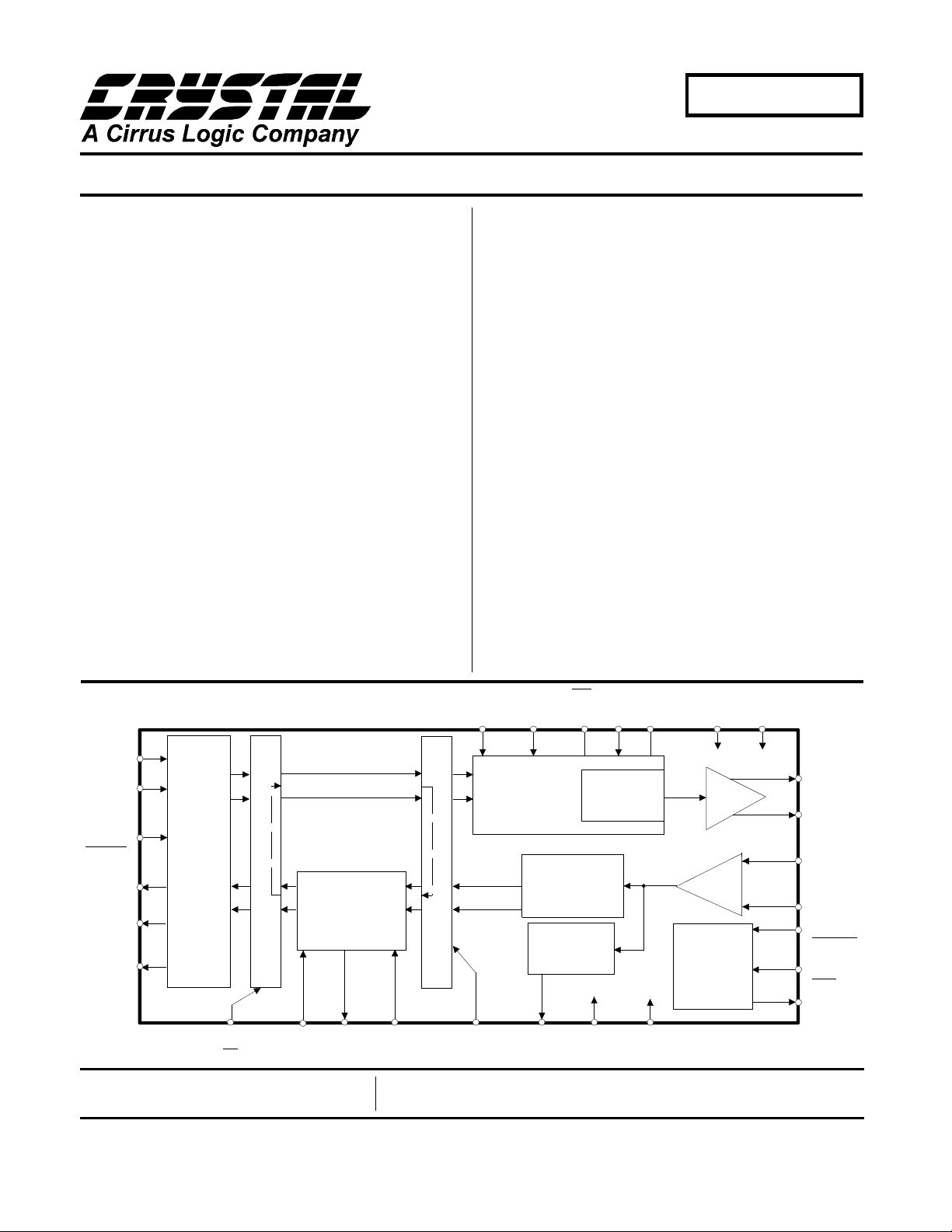
T1/E1 Line Interface
CS61577
Features
Provides Analog Transmission Line
•
Interface for T1 and E1 Applications
Drop-in Replacement for CS61574 with
•
the Following Enhancements:
- Lower Power Consumption
- Transmitter Short-Circuit
Current Limiting
- Greater Transmitter Immunity
to Line Reflections
- Software Selection Between 75Ω and
120Ω E1 Output Options
- Internally Controlled E1 Pulse Width
- B8ZS/HDB3/AMI Encoder/Decoder
General Description
The CS61577 is a drop-in replacement for the
CS61574, and combines the complete analog transmit
and receive line interface for T1 or E1 applications in a
low power, 28-pin device operating from a +5V supply.
The CS61577 supports processor-based or standalone operation and interfaces with industry standard
T1 and E1 framers.
The receiver uses a digital Delay-Locked-Loop which is
continuously calibrated from a crystal reference to provide excellent stability and jitt er tolerance. The receiver
includes a jitter attenuator optimized for minimum delay
in switching and transmission applications. The transmitter provides internal pulse shaping to insure
compliance with T1 and E1 pulse template specifications.
Applications
• Interfacing Network Equipment such as DACS and
Channel Banks to a DSX-1 Cross Connect
• Building Channel Service Units
ORDERING INFORMATION
CS61577-IP1 28 Pin Plastic DIP
CS61577-IL1 28 Pin Plastic PLCC
TCLK
TPOS
[TDATA]
TNEG
[TCODE]
RCLK
RPOS
[RDATA]
RNEG
[BPV]
( ) = Pin Function in
[ ] = Pin Function in
2
3
4
AMI,
B8ZS,
HDB3,
8
CODER
7
6
RLOOP
(CS)
Host Mode
Extended Hardware Mode
R
E
M
O
T
E
L
O
O
P
B
A
C
K
26
XTALIN
JITTER
ATTENUATOR
9
XTALOUT10ACLKI
Preliminary Product Information
Crystal Semiconductor Corporation
P. O. Box 17847, Austin, Texas, 78760
(512) 445-7222 FAX:(512) 445-7581
MODE
L
O
C
A
L
L
O
O
P
B
A
C
K
1
LLOOP
(SCLK)
(CLKE)
TAOS
5
CONTROL
27
(INT)
LEN0
28 23
CLOCK &
DATA
RECOVERY
SIGNAL
QUALITY
MONITOR
12 21
LOS
(SDI)
(SDO)
LEN1
LEN2
2524
PULSE
SHAPER
LINE RECEIVER
RV+22RGND
TGND
14
LINE DRIVER
DRIVER
MONITOR
TV+
15
13
16
19
20
17
18
11
TTIP
TRING
RTIP
RRING
MTIP
[RCODE]
MRING
[PCS]
DPM
[AIS]
This document contains information for a new product. Crystal
Semiconductor re ser ve s th e rig ht to modify this product wit hout n otic e.
Copyright Crystal Semiconductor Corporation 1996
(All Rights Reserved)
MAY ’96
DS155PP2
1
CS61577
ABSOLUTE MAXIMUM RATINGS
Parameter Symbol Min Max Units
DC Supply (referenced to RGND=TGND=0V) RV+
TV+
Input Voltage, Any Pin (Note 1) V
Input Current, Any Pin (Note 2) I
Ambient Operating Temperature T
Storage Temperature T
in
in
A
stg
-
-
6.0
(RV+) + 0.3
RGND-0.3 (RV+) + 0.3 V
-10 10 mA
-40 85
-65 150
WARNIN G: O perat ions at or beyond these l imits may resul t in perma nent da mage to t he devi ce.
Normal operation is not guaranteed at these extremes.
Notes: 1. Excluding RTIP, RRING, whic h must stay wit hin -6V to (RV+ ) + 0.3V.
2. Transient currents of up to 1 00 mA will not cause SCR la tch-up. Also TTIP, TRING, TV+ and TGND
can withstand a continuous current of 100 mA.
RECOMMENDED OPERATING CONDITIONS
Parameter Symbol Min Typ Max Units
DC Supply (Note 3) RV+, TV+ 4.75 5.0 5.25 V
Ambient Operating Temperature T
Power Consumption (Notes 4,5) P
Power Consumption (Notes 4,6) P
Notes: 3. TV+ must not exceed RV+ by more than 0.3V.
4. Power consumption while driving line load over operating temperature range. Includes IC and load.
Digital input levels are within 10% of the supply rails and digital outputs are driving a 50 pF
capacitive load.
5. Assumes 100% ones density and maximum line length at 5.25V.
6. Assumes 50% ones density and 300ft. line length at 5.0V.
A
C
C
-40 25 85
-400500mW
-230-mW
V
V
°C
°C
°C
DIGITAL CHARACTERISTICS (TA = -4 0°C to 85°C; T V+, RV+ = 5.0V ± 5%; GND = 0V)
Parameter Symbol Min Typ Ma x Units
High-Level Input Voltage (Notes 7, 8)
V
IH
PINS 1-4 , 17, 18 , 23-28
Low-Level Input Voltage (Notes 7, 8)
V
IL
PINS 1-4 , 17, 18 , 23-28
High-Level Output Voltage (Notes 7, 8, 9)
I
= -40 µA PINS 6-8, 11, 12, 25
OUT
Low-Level Output Voltage (Notes 7, 8, 9)
I
= 1.6 mA PINS 6-8, 11, 12, 23, 25
OUT
V
OH
V
OL
Input Leakage Current (Except Pin 5) - Low-Level Input Voltage, PIN 5 V
High-Level Input Voltage, PIN 5 V
Mid-Level Input Voltage, PIN 5 (Note 10) V
IL
IH
IM
Notes: 7. In Extended Hardware Mode, pins 17 and 18 are digital inputs. In Host Mode, pin 23 is
an open drain output and pin 25 is a tristate output.
8. This specification guarantees TTL compatibility (V
= 2.4V @ I
OH
9. Output drivers will drive CMOS logic levels into a CMOS load.
10. As a n a lter nat ive t o suppl yin g a 2.3- to -2.7 V in put, th is pin may b e le ft flo ati ng.
2 DS155PP2
2.0 - - V
--0.8V
4.0 - - V
--0.4V
±10 µA
--0.2V
(RV+) - 0.2 - - V
2.3 - 2.7 V
= -40µA).
OUT

CS61577
ANALOG SPECIFICATIONS (TA = -40°C to 85°C; TV+, RV+ = 5. 0V ±5%; GND = 0V)
Parameter Min Typ Max Units
Transmitter
AMI Output Pulse Amplitudes (Note 11)
E1, 75 Ω (Note 12)
E1, 120 Ω (Note 13)
T1, (FCC Part 68) (Note 14)
T1, DSX-1 (Note 15)
Load Presented To Transmitter Output (Note 11) - 25 Jitter Added During Remote Loopback (Note 16)
10Hz - 8kHz
8kHz - 40k Hz
10Hz - 40k Hz
Broad Band
Power in 2kHz band about 772kHz (Notes 11, 17) 12.6 15 17.9 dBm
Power in 2kHz band about 1.544MHz (Notes 11, 17)
(referenced to power in 2kHz band at 772kHz)
Positive to Negative Pulse Imbalance (Notes 11, 17) - 0.2 0.5 dB
Transmitter Output Impedance (Notes 17, 18) - - 10
Transmitter Short Circuit Current (Notes 11, 19) - - 50 mA RMS
Notes: 11. Usi ng a 0.47 µF capacitor in series with the primary of a transformer recommended
in the Applications Section.
12. Pulse amplitude measured at the output of the transformer across a 75 Ω load for line length
settings LEN2/1/0 = 0/0/1 and 0/0/0. For LEN2/1/0 = 0/0/0 only, a 4.4 Ω resistor is required
in series with the transformer primary.
13. Pulse amplitude measured at the output of the transformer across a 120 Ω load for line length
setting LEN2/1/0 = 0/0/0.
14. Pulse amplitude measured at the output of the transformer across a 100 Ω load for line length
setting LEN2/1/0 = 0/1/0.
15. Pulse amplitude measured at the DSX-1 Cross-Connect for all line length settings from
LEN2/1/0 = 0/1/1 to LEN2/1/0 = 1/1/1.
16. Input signal to RTIP/RRING is jitter free. Values will reduce slightly if jitter free clock is input to TCLK.
17. Not production tested. Parameters guaranteed by design and characterization.
18. Measured between the TTIP and TRING pins at 772 kHz during marks and spaces.
19. Measured broadband through a 0.5 Ω resistor across the secondary of the transmitter transformer
during the transmission of an all ones data pattern with LEN2/1/0 = 0/0/0 or 0/0/1.
2.14
2.7
2.7
2.4
-
-
-
-
-29 -38 - dB
2.37
3.0
3.0
3.0
0.005
0.008
0.010
0.015
2.6
3.3
3.3
3.6
-
-
-
-
V
V
V
V
Ω
UI
UI
UI
UI
Ω
DS155PP2 3

CS61577
ANALOG SPECIFICATIONS (TA = -40°C to 85°C; TV+, RV+ = 5. 0V ±5%; GND = 0V)
Parameter Min Typ Max Units
Receiver
RTIP/RRING Input Impedance - 50k Sensitivity Below DSX (0dB = 2.4V) -13.6
500
Loss of Signal Threshold - 0.30 - V
Data Decision Threshold
T1, DSX-1 (Note 20)
T1, DSX-1 (Note 21)
T1, (FCC Part 68) and E1 (Note 22)
60
53
45
Allowable Consecutive Zeros before LOS 160 175 190 bits
Receiver Input Jitter Tolerance (Note 23)
10kHz - 100kHz
2kHz
10Hz and below
0.4
6.0
300
Jitter Attenuator
Jitter Attenuation Curve Corner Frequency (Notes 17, 24) - 6 - Hz
Attenuation at 10kHz Jitter Frequency (Notes 17, 24) - 50 - dB
Attenuator Input Jitter Tolerance (Before Onset
12 23 - UI
of FIFO Overflow or Underflow Protection) (Notes 17, 24)
Notes: 20. For input amplitude of 1.2 V
21. For input amplitude of 0.5 V
22. For input amplitude of 1.05 V
to 4. 14 Vpk.
pk
to 1.2 Vpk and from 4. 14 Vpk to RV+.
pk
to 3.3 Vpk.
pk
23. Jitter tolerance increases at lower frequencies. See Figure 11.
24. Attenuation measured with input jitter equal to 3/4 of measured jitter tolerance. Circuit attenuates
jitter at 20 dB/decade above the corner frequency. See Figure 12. Output jitter can increase
significantly when more than 12 UI’s are input to the attenuator. See discussion in the text section.
65
65
50
-
-
-
-
-
70
77
55
-
-
dB
mV
% of peak
% of peak
% of peak
-
-
-
UI
UI
UI
Ω
4 DS155PP2
CS61577
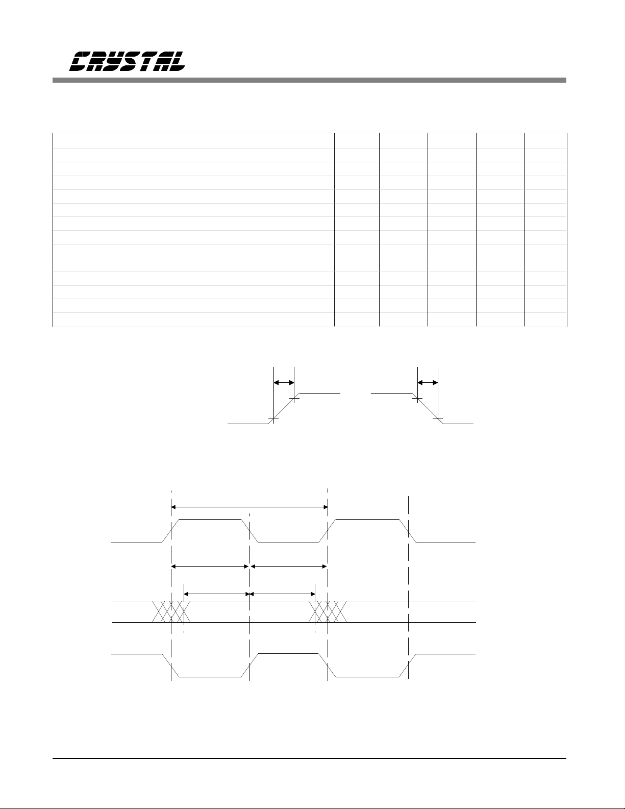
T1 SWITCHING CHARACTERISTICS (TA = -40°C to 85°C; TV+, RV+ = 5.0V ±5%;
GND = 0V; Inputs: Logic 0 = 0V, Logic 1 = RV+; See Figures 1, 2, & 3)
Parameter Symbol Min Typ Max Units
Crystal Frequency (Note 25) f
TCLK Frequency f
ACLKI Frequency (Note 26) f
RCLK Duty Cycle (Note 27) t
Rise Time, All Digital Outputs (Note 28) t
Fall Time, All Digital Outputs (Note 28) t
TPOS/TNEG (TDATA) to TCLK Falling Setup Time t
TCLK Falling to TPOS/TNEG (TDATA) Hold Time t
RPOS/RNEG Valid Before RCLK Falling (Note 29) t
RDATA Valid Before RCLK Falling (Note 30) t
RPOS/RNEG Valid Before RCLK Rising (Note 31) t
RPOS/RNEG Valid After RCLK Falling (Note 29) t
RDATA Valid After RCLK Falling (Note 30) t
RPOS/RNEG Valid After RCLK Rising (Note 31) t
c
tclk
aclki
pwh1/tpw1
r
f
su2
h2
su1
su1
su1
h1
h1
h1
Notes: 25. Crystal must meet specifications described in CXT6176/CXT8192 data sheet.
26. ACLKI provided by an external source or TCLK.
27. RCLK duty cycle will be 62.5% o r 37.5% when jitte r attenuator limit s are reach ed.
28. At max load of 1.6 mA and 50 pF.
29. Host Mode (CLKE = 1).
30. Extended Hardware Mode.
31. Hardware Mode, or Host Mode (CLKE = 0)
32. The transmitted pulse width does not depend on the TCLK duty cycle.
- 6.176000 - MHz
-1.544-MHz
-1.544-MHz
45 50 55 %
- - 85 ns
- - 85 ns
25 - - ns
25 - - ns
150 274 - n s
150 274 - n s
150 274 - n s
150 274 - n s
150 274 - n s
150 274 - n s
E1 SWITCHING CHARACTERISTICS (TA = -4 0°C to 85 °C; TV+, RV+ = 5.0V ±5%;
GND = 0V; Inputs: Logic 0 = 0V, Logic 1 = RV+; See Figures 1, 2, & 3)
Parameter Symbol Min Typ Max Units
Crystal Frequency (Note 25) f
TCLK Frequency f
TCLK Duty Cycle for LEN2/1/0 = 0/0/0 (Note 32) t
ACLKI Frequency (Note 26) f
RCLK Duty Cycle (Note 27) t
Rise Time, All Digital Outputs (Note 28) t
Fall Time, All Digital Outputs (Note 28) t
TPOS/TNEG (TDATA) to TCLK Falling Setup Time t
TCLK Falling to TPOS/TNEG (TDATA) Hold Time t
RPOS/RNEG Valid Before RCLK Falling (Note 29) t
RDATA Valid Before RCLK Falling (Note 30) t
RPOS/RNEG Valid Before RCLK Rising (Note 31) t
RPOS/RNEG Valid After RCLK Falling (Note 29) t
RDATA Valid After RCLK Falling (Note 30) t
RPOS/RNEG Valid After RCLK Rising (Note 31) t
c
tclk
pwh2/tpw2
aclki
pwh1/tpw1
r
f
su2
h2
su1
su1
su1
h1
h1
h1
DS155PP2 5
- 8.192000 - MHz
-2.048-MHz
40 50 60 %
-2.048-MHz
45 50 55 %
- - 85 ns
- - 85 ns
25 - - ns
25 - - ns
100 194 - n s
100 194 - n s
100 194 - n s
100 194 - n s
100 194 - n s
100 194 - n s
SWITCHING CHARACTERISTICS (TA = -40 ° to 85°C; TV +, RV+ = ±5% ;
Inputs: Logic 0 = 0V, Logic 1 = RV+)
Parameter Symbol Min Typ Max Un its
SDI to SCLK Setup Time t
SCLK to SDI Hold Time t
SCLK Low Time t
SCLK High Time t
SCLK Rise and Fall Time t
CS to SCLK Setup Time t
SCLK to CS Hold Time t
CS Inactive Time t
SCLK to SDO Valid (Note 33) t
CS to SDO High Z t
Input Valid To PCS Falling Setup Time t
PCS Rising to Input Invalid Hold Time t
PCS Active Low Time t
Notes: 33. Output load capacitance = 50pF
dc
cdh
cl
ch
, t
r
cc
cch
cwh
cdv
cdz
su4
h4
pcsl
f
50 - - ns
50 - - ns
240 - - ns
240 - - ns
- - 50 ns
50 - - ns
50 - - ns
250 - - ns
- - 200 ns
- 100 - ns
50 - - ns
50 - - ns
250 - - ns
CS61577
RCLK
RPOS
RNEG
RDATA
BPV
RCLK
Any Digital Output
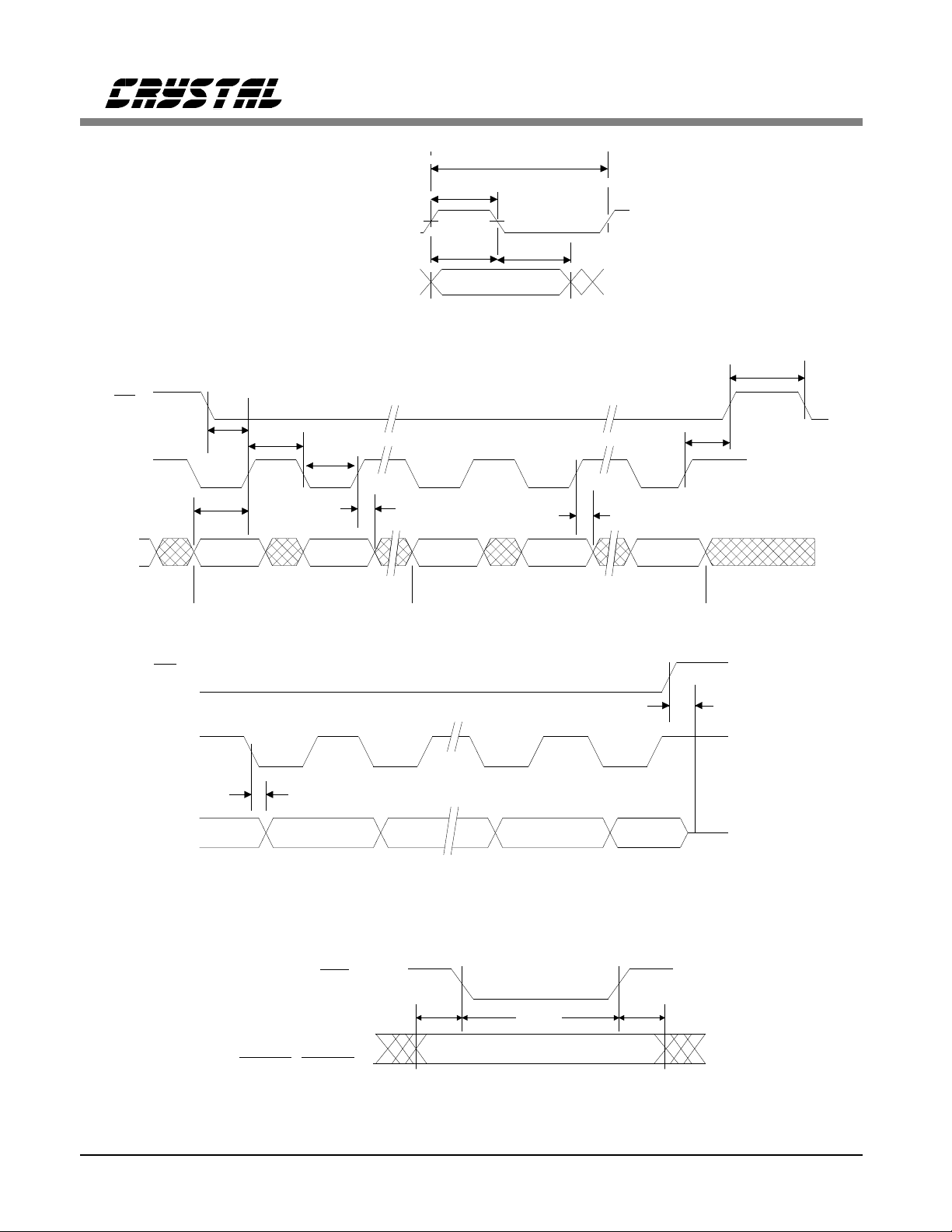
Figure 1. Signal Rise and Fall Characteristics
t
t
pwl1
tt
su1
pw1
t
r
90% 90%
10%
t
pwh1
h1
10%
t
f
EXTENDED
HARDWARE
MODE OR
HOST MODE
(CLKE = 1)
HARDWARE
MODE OR
HOST MODE
(CLKE = 0)
Figure 2. Recovered Clock and Data Switching Characteristics
6 DS155PP2
t
pwh2
t
pw2
CS61577
CS
SCLK
SDI
TCLK
t
su2
t
h2
TPOS/TNEG
Figure 3. Transmit Clock and Data Switching Characteristics
t
t
cc
t
dc
LSB LSB
ch
CONTROL BYTE DATA BYTE
t
cl
t
cdh
Figure 4. Serial Port Write Timing Diagram
t
cdh
MSB
t
cch
t
cwh
CS
SCLK
SDO
CLKE = 1
t
cdv
Figure 5. Seria l Port R ead Timi ng Di agra m
PCS
t
h4
LEN0/1/2 , T A OS,
RLOOP, LLOOP,
RLOOP, LLOOP,
t
su4
t
pcsl
VALID INPUT DATA
RCODE, TCODE
Figure 6. Exte nded Ha rdwa re Mo de Par allel Chip Select Timin g Dia gram
t
cdz
HIGH Z
DS155PP2 7
CS61577
THEORY OF OPERATION
CS61577 Enhancement s Relative to CS61 574
Existing design s using the CS61574 can be converted to th e higher perform ance, pin-co mpatible
CS61577 with no changes to the PCB, external
component or system software.
The CS61577 provides higher performance and
more features than the CS61574 including:
• Selection of 75 Ω or 120 Ω E1 outpu t op-
tions under software or hardware control,
• 50 mA
transmitter short-ci rcuit current
RMS
limiting for E1 (per OFTEL OTR-001),
• internally co ntrolled puls e width for E1
output options,
• 35% lower power consumption,
• Increased transmit ter immunity to signal re-
flections for improved signal qu ality,
• Optional AMI, B8ZS, HDB3 enc oder/de-
coder or external line coding support,
• Receiver AIS (unframed all on es) detect ion,
• Improved receiver Loss of Signal handling
(LOS set at power-up, reset upon receipt of
3 ones in 32 bit pe riods with no more t han
15 consecutive zeros),
• Transmitter TTIP and TRING ou tputs are
forced low when TCLK is static,
• The Driver Performan ce Monitor op erates
over a wider range of input signal levels.
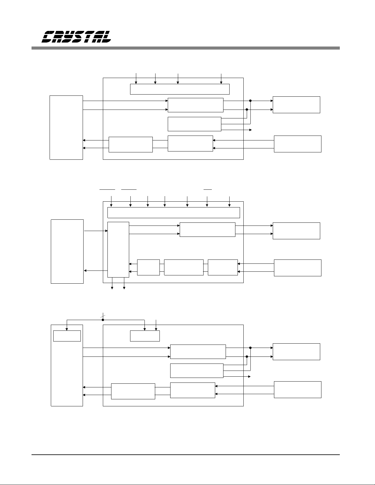
Introduction to Op erating Modes
The CS61577 supports three operating modes
which are selected by the level of the MODE pin
as shown in Tables 1 and 2, Figure 7, and Figures
A1-A3 of the Applications section.
The modes are Har dware Mode, Extended Hardware Mode, and Host Mode. In Hardware and
Extended Hardware Modes, discret e pins are used
to configure and monitor the device. The Extended Hardware Mode provides a parallel chip
select input which latches the control inputs al-
lowing individual ICs to be configured using a
common set of control lines. In the Host Mode,
an external processor monito rs and configures the
device through a serial interface. There are thirteen multi-function pins whose functionality is
determined by the operating mode. (see Table 2).
Hardware
Mode
Control
Method
MODE
Pin
Level
Line
Coding
AIS
Detection
Driver
Performance
Monitor
Table 1. Diff erences Betwe en Operati ng Modes
FUNCTION PIN HARDWARE
TRANSMITTER
RECEIVER/DPM
CONTROL
Control
Pins
<0.2 V Floating or
External Internal-
No Yes No
Yes No Yes
3TPOS TDATA TPOS
4TNEG
6 RNEG B PV RNEG
7RPOS RDATA RPOS
11 DPM AIS DPM
17 MTIP
18 MRING - MRING
18 23 LEN0 LEN0
24 LEN1 LEN1 SDI
25 LEN2 LEN2 SDO
26 RLOOP RLOOP
27 LLOOP LLOOP SCLK
28 TAOS TAOS CLKE
Table 2. Pin Definitions
Extended
Hardware
Mode
Control Pins
with Parallel
Chip Select
2.5 V
AMI, B8ZS,
or HDB3
MODE
EXTENDED
HARDWARE HOST
TCODE TNEG
RCODE MTIP
PCS -
Host
Mode
Serial
Interface
>(R V+)-0.2 V
External
INT
CS
8 DS155PP2
CS62180B
FRAMER
CIRCUIT
TNEG
RPOS
RNEG
CS61577
JITTER
ATTENUATOR
EXTENDED HARDWARE MODE
HARDWARE MODE
RLOOP LEN0/1/2LLOOPTAOS
CONTROL
LINE DRIVER
DRIVER MONITOR
LINE RECEIVER
MRING
MTIP
TTIPTPOS
TRING
DPM
RTIP
RRING
CS61577
TRANSMIT
TRANSFORMER
RECEIVE
TRANSFORMER
T1 or E1
REPEATER
OR
MUX
CONTROL
CS62180B
FRAMER
CIRCUIT
TDATA
CODER
RDATA
BPV AIS
µ
P SERIAL POR T
5
TPOS
TNEG
RPOS
RNEG
RCODETCODE
AMI
B8ZS,
HDB3,
CS61577
JITTER
ATTENUATOR
CS61577
AIS
DETECT
CLKE
CONTROL
RLOOP PCS LEN0/1/2LLOOPTAOS
CONTROL
JITTER
ATTENUATOR
HOST MODE
LINE DRIVER
DRIVER MONITOR
LINE RECEIVER
LINE DRIVER
RECEIVER
LINE
MRING
MTIP
TTIP
TRING
RTIP
RRING
TTIP
TRING
DPM
RTIP
RRING
TRANSMIT
TRANSFORMER
RECEIVE
TRANSFORMER
TRANSMIT
TRANSFORMER
RECEIVE
TRANSFORMER
Figure 7. Overv iew of Op eratin g Mode s
DS155PP2 9
CS61577
Transmitter
The transmitter takes digita l T1 or E1 input data
and drives appropriately shaped bipolar pulses
onto a transmission line through a 1:2 transformer. The transmit data (TPOS & TNEG or
TDATA) is supplied synchronously and sampled
on the falling edge of the input clock, TCLK.
Either T1 (DSX-1 or Network Interface) or E1
CCITT G.703 pulse shapes may be selected.
Pulse shaping and signal level are controlled by
"line length selec t" inputs as shown in Table 3.
For T1 DSX-1 applications, line lengths from 0 to
655 feet (a s measured from t he transmitter to the
DSX-1 cross conne ct) may be selected. The five
partition arrangement in Table 3 meets ANSI
T1.102 and AT&T CB-119 requirements when
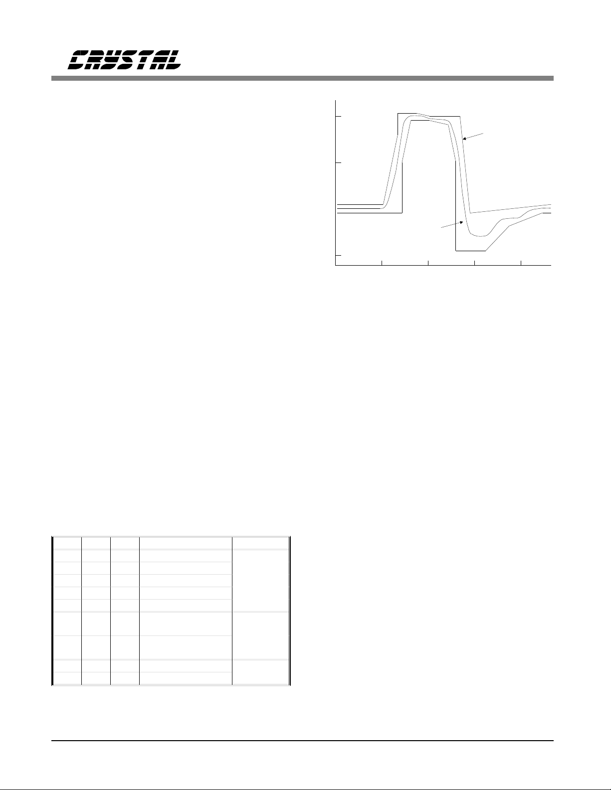
using #22 ABAM cable. A typica l outpu t pulse is
shown in Figure 8. The se pulse settings can also
be used to meet CCITT pul se shape require ments
for 1.544 MHz operation.
For T1 Network In terface applicat ions, two add itional opti ons are provided. Not e that the o ptimal
pulse width for Part 68 (324 ns) is narrower than
the optimal pu lse width for DSX-1 (350 ns ). The
CS61577 automatically adjusts the pulse width
based upon the "line length" selection made.
NORMALIZED
AMPLITUDE
1.0
0.5
0
OUTPUT
PULSE SHAPE
-0.5
0
Figure 8. Typical Pulse Shape at DSX-1 Cross Connect
250 750 1000
500
TIME (nanoseconds)
ANSI T1.102,
AT&T CB 119
SPECIFICATIONS
The E1 G.703 p ulse shape is supported wi th line
length selections LEN2/1/0=0/0/0 or
LEN2/1/0=0/0/1. As with the CS61574,
LEN2/1/0=0/0 /0 supports the 120 Ω, 3 V o utput
option without external series resistors, but will
also support the 75 Ω, 2.37 V output optio n with
an external 4.4 Ω resistor in series with TTIP or
TRING. The new LEN2/1/0=0/0 /1 code supports
the 75 Ω, 2.37 V outpu t option without external
series resistors allowing for software selection between the two E1 output opti ons. The pulse width
will meet th e G.703 pulse shape template shown
in Figure 9, and specified in Table 4.
The CS61577 wi ll detect a static TCL K, and will
force TTIP and TRING low to prevent trans mis-
LEN2 LEN1 LEN0 Option Selected Application
0 1 1 0-133 FEET
100 133-266 FEET
101 266-399 FEET
110 399-533 FEET
111 533-655 FEET
000
001
0 1 0 FCC PART 68, OPT. A NETWORK
011 ANSI T1.403
Table 3. Line Length Selection
10 DS155PP2
75 Ω (with 4.4 Ω
resistor) & 120 Ω
75 Ω (without
4.4 Ω resistor)
DSX-1
ABAM
(AT&T 600B
or 600C)
E1
CCITT G.703
INTERFACE
sion when data is not present. When any transmit
control pin (TAOS, LEN0-2 or LLOOP) is toggled, the transmitter outputs will require
approximately 22 bit periods to stabilize. The
transmitter will take longer to stabilize when
RLOOP is selected because the timing circuitry
must adjust to the new frequency.
CS61577
Percent of
nominal
peak
voltage
120
110
100
90
80
50
10
0
-10
-20
Figure 9. Mask of the Pulse at the 2048 kbps Interface
269 ns
244 ns
194 ns
Nominal Pulse
219 ns
488 ns
Transmit All Ones Select
The transmitter provides for all ones insertion at
the frequency of TCLK. Transmit all ones is selected when TAOS goes high, and causes
continuous ones to be transmitted on the line
(TTIP and T RING). In this mode , the TPOS and
TNEG (or TDATA) inputs are ignore d. If Remote
Loopback is in effect, any TAOS request will be
ignored.
Receiver
The receiver extracts dat a an d cl ock fro m an AMI
(Alternate Mark Inversion) coded signal and outputs clock an d synchronized data. The receiver is
sensitive to signals over the entire range of
ABAM cable lengths and requires no equalizati on
or ALBO (Automatic Line Build Out) circuits.
The signal is received on both ends of a centertapped, center-grounded transformer. The
transformer is center tapped on the IC side. The
clock and dat a recovery circuit exceeds the jitter
tolerance specifications of Publications 43802,
43801, AT&T 62411, TR-TSY-000170, and
CCITT REC. G.823.
A block diagram of the rec eiver is shown in Figure 10. The two leads of the transformer (RTIP
and RRING) have oppos ite polarity allowing the
receiver to treat RTIP and RRING as unipolar signals. Comparators are used to detect pulses on
RTIP and RRING. The co mparator th resholds are
dynamically established a t a percent of the peak
level (50% of peak for E1, 65% of peak for T1;
with the slicing level selected by LEN2/1/0 inputs).
The leading ed ge of an incoming data pul se triggers the clo ck phase selector. The phase selector
chooses o ne of the 13 available ph ases which the
delay line pr oduces for each bit period. T he out-
For coaxial cable,
75Ω load and
transformer specified
in Application Section.
Nominal peak voltage of a mark (pulse) 2.37 V 3 V
Pea k voltage of a space (no pulse)
Nominal puls e wi dt h 244 ns
Ratio of the amplitudes of positive and negative
pulses at the center of the pulse interval
Ratio of the widths of positive and negative
pulses at the nomi nal half amplitude
* When configured with a 0.47 µF nonpolarized capacitor in series with the TX transformer
primary as shown in Figures A1, A2 and A3.
Table 4. CCITT G.703 S pecificati ons
DS155PP2 11
0 ±0.237 V 0 ±0.30 V
0.95 to 1.05*
0.95 to 1.05*
For shielded twisted
pair, 120Ω load and
transformer specified
in Application Section.
CS61577
RTIP
1 : 2
RRING
Data
Level
Slicer
Edge
Detector
Figure 1 0. Re cei ver Bl oc k Di agr am
put from the phase selector feeds the clock and
data recovery circuits which generate the recovered clock and sample the incoming signal at
appropriate intervals to recover the data.
Data sampling will continue at the periods selected by the phase selector until an incoming
pulse deviates enou gh to cause a new phase to be
selected for da ta sampling. The phases of the d elay line are selected and updated to allow as much
as 0.4 UI of jitter from 10 kHz to 100 kHz, without error. The jitter tolerance of the receiver
exceeds that shown in Figure 11. Additionally,
this method o f clock and d ata recovery is tol erant
of long strings of consecutive zeros. The data
Minimum
Performance
PEAK-TO-PEAK
JITTER
(unit intervals)
300
138
100
AT&T 62411
28
10
Data
Sampling
& Clock
Extraction
Clock
Phase
Selector
Continuously
Calibrated
Delay Line
Jitter
Attenuator
RPOS
RNEG
RCLK
sampler will continuously sample data based on
its last input until a new pulse arrives to update
the clock phase selector.
The delay line is continuously calibrated using
the crystal oscillator reference clock. The delay
line produces 13 phases for eac h cycle of the reference clock. In effect, the 13 phases are
analogous to a 20 MHz clock when the reference
clock is 1.544 MHz. This implementation utilizes
the benefits of a 2 0 MHz clo ck for cl ock recovery
without actually having the clock present to impede analog circuit performance.
In the Hardware Mode, d ata at RPOS and RNEG
should be sampled on th e rising edge of RCLK,
the recovered clock. In the Extended Hardware
Mode, data at RDATA shou ld be sampled on the
falling edge of RCLK. In the Host Mode, CLKE
determines the clock polarity for which output
data should be sampled as s hown in Table 5.
1
.4
.1
1
10 1k 10k
100 100k700
300
JITTER FREQUENCY (Hz)
Figure 11. Minimum Input Jitter Tolerance of Receiver
(Clock Reco very C ircui t and Jitt er Atte nua tor)
12 DS155PP2

CS61577
MODE
(pin 5)
LOW
(<0.2V)
HIGH
(>(V+) - 0.2V)
HIGH
(>(V+) - 0.2V)
MIDDLE
(2.5V)
X = Don’t Care
Table 5. Data Ou tput/Clock Relatio nship
CLKE
(pin 28) DATA CLOCK
RPOS
X
RNEG
LOW
HIGH
RPOS
RNEG
SDO
RPOS
RNEG
SDO
X RDATA RCLK Falling
RCLK
RCLK
RCLK
RCLK
SCLK
RCLK
RCLK
SCLK
Clock Edge for
Valid Data
Rising
Rising
Rising
Rising
Falli ng
Falli ng
Falli ng
Rising
Loss of Signal
The receiver will indicate loss of signal after
power-up, reset or upon receiving 175 consecutive zeros. A digital counter counts received
zeros, base d on RCLK cycles. A zero is received
when the RTIP and RRING inputs are below the
input comparator slicing threshold level established by the peak detector. After the signal is
removed for a period of time the data slicing
threshold level decays to approximately
300 mV
peak
.
The receiver reports loss of s ignal by setting the
Loss of Signal p in, LOS, high. If the serial interface is used, the LOS bit will be set and an
interrupt will be issued on
LOS will return low (asserting the
INT (unless disabled).
INT pin again
in Host Mode) upon receipt of 3 ones in 32 bit
periods with no more t han 15 consecutive zeros.
Note that in the Host Mode, LOS is simultaneously available from both the register and pin 12.
RPOS/RNEG or RDATA are forced low during
LOS unless the jitter attenuator is dis abled. (See
"Jitter Attenuator" section)
If ACLKI is present during the LOS st ate, ACLKI
is switched int o the input of the jitter attenua tor,
resulting in RCLK matching the frequency of
ACLKI. The jitter attenuator buffers any inst antaneous changes in phase between the last
recovered clock and the ACLKI reference clock.
This means that RCLK will smoothly transition
to the new frequency. If ACLKI is not present,
then the crysta l osci lla tor of the jit ter atte nua tor is
forced t o its center frequ ency. Table 6 shows the
status of RCLK upon LOS.
Crystal
present?
No Yes ACLKI
Yes No Center ed Crysta l
Yes Yes
ACLKI
present?
Table 6. RC LK Stat us at L OS
Source of RCLK
ACLKI via t he
Jitter Attenuator
Jitter Attenuator
The jitter at tenuator reduces wander and jitte r in
the recovered cl ock signal. It consists of a 32-bit
FIFO, a crystal os cillator, a set o f load ca pacitors
for the crystal, and control log ic. The jitter attenuator exceeds the jit ter attenu ation requi rements of
Publication s 43802 and REC. G.742.
The jitter attenu ator works in the following manner. The recovered clock and data are in put to t he
FIFO with the recovered clock controlling the
FIFO’s write pointer. The crystal oscillator controls the FIFO’s read pointer which reads data out
of the FIFO and presents it at RPOS and RNEG
(or RDATA). The u pdate rate of the read p ointer
is analogous to RCLK. By chang ing the load capacitance that the IC presents to the crystal, the
oscillation frequency is adjusted to the average
frequency of the recovered signal. Logic determines the phase relationship between the read and
write pointe rs and decid es how to adjust the lo ad
capacitance of the crystal. Thus th e jitter attenuator behaves as a first-order phase lock loop. Jitter
is absorbed in the FIFO according to the jitter
transfer ch ar acteristic s h own in Figure 12.
DS155PP2 13
CS61577
0
a) Minimum Attenuati on Limit
10
20
30
b) Maximum
40
Attenuation in dB
Attenuation
Limit
50
60
110
Figure 12. Typ ical Jitte r Tr ansf er Fun ction
62411 Requirements
Measured Performance
100
Frequency in Hz
1 k 10 k
The FIFO in the jitter attenuator is designed to
prevent overflow and underflow. If the jitter amplitude becomes very large, the read and write
pointers may get very clos e together. Should they
attempt to cross, the oscillator’s divide by four
circuit adjusts by performing a divide by 3 1/2 or
divide by 4 1/2 to prevent the overflow or underflow. During this activity, data will never be lost.
Local Loopback
Local loopbac k is selected by taking LLOOP, pin
27, high or by setting the LLOOP register bit via
the serial interface.
The local loopback mode takes clock and data
presented on TCLK, TPOS, and TNEG (or
TDATA), sends it through the j itter a tte nuator a nd
outputs it at RCLK, RPOS and RNEG (or
RDATA). If the jitter attenuator is disabled, it is
bypassed. Inputs to the tr ansmitter are still transmitted on TTIP and TRING, unless TAOS has
been selec ted in which case, AMI-coded conti nuous ones are tra nsmitted at the TCLK freq uency.
The receiver RT IP and RRING inp uts are igno red
when local loopback is in effect.
Remote Loopback
Remote loopback is selected by taking RLOOP,
pin 26, high o r by settin g the RLOOP register bit
via the serial interface.
The 32-bit FIFO in the CS61577 attenuator allows it to absorb jitter with minimum dat a d elay
in T1 and E1 switching or transmission applications. Like the CS61574, the CS61577 will
tolerate large amplitude jitter (>23 UIpp) by
tracking rather than attenuating it, preventing data
errors so that the jitter may be absorbed in external frame buffers.
The jitter at tenuator may be bypass ed by pulling
XTALIN to RV+ through a 1 kΩ resistor and pro-
viding a 1.544 MHz (or 2.048 MHz) clock on
ACLKI. RCLK may exhibit quantiza tion jitter of
approximately 1/13 UIpp and a duty cycle of approximately 30% (70%) when the attenuator is
disabled.
In remote loopbac k, the re covered clock and da ta
input on RTIP and RRING are sent through the
jitter attenuato r and back ou t on the lin e via TTIP
and TRING. Selecting remote loo pback overrides
any TAOS request (see Table 6). The recovered
incoming signals are also sent to RCLK, RPOS
and RNEG (or RDATA). A remote loopbac k occurs in response to RLOOP going high.
RLOOP
Input
Signal
Notes: 1. X = Don’t Care. The identified All Ones Select
TAOS
Input
Signal
00 TDATA TCLK
0 1 all 1s TCLK
1 X RTIP & RRING RTIP & RRING (RCLK)
input is ignored when the indicated loopback is
in effect.
2. Logic 1 indicates that Loopback or All Ones
option i s sele ct ed.
Table 7. Interaction of RLOOP wi th TAOS
Source of
Data for
TTIP & TRING
Source of
Clock for
TTIP & TRING
14 DS155PP2

CS61577
Simultaneou s selection of local and remote loopback modes is not valid (see Reset).
In the Extended Hardware Mode the transmitted
data is looped before the AMI/B8ZS/HDB3 encoder/decoder du ring remot e loopbac k so that th e
transmitted signal matches the received signal,
even in the presence of received bipolar violations. Data output on RDATA is decoded,
however, if
RCODE is low.
Alarm Indication Signal
In the Extended Hardware Mode, the receiver sets
the output pin AIS high when less than 3 zeros
are detected out of 2048 bit periods.
Line Code Encoder/De coder
In the Extend ed Hardware Mode , three line codes
are available: AMI, B8ZS a nd HDB3. The input
to the encoder is TDATA. The outputs from the
decoder are RDATA and BPV (Bipol ar Violatio n
Strobe). The encoder and decoder are selected
using the LEN2, LEN1, LEN0,
TCODE and
RCODE pins as shown in T a ble 8.
LEN 2/1/0
000 010-111
TCODE
(Transmit
Encoder
Selection)
RCODE
(Receiver
Decoder
Selection)
Table 8. Encoder/Decoder Selection
LOW
HIGH AMI Encoder
LOW
HIGH AMI Decoder
HDB3
Encoder
HDB3
Decoder
B8ZS
Encoder
B8ZS
Decoder
Parallel Chip Select
In the Extended Hardware Mode,
used to gate the digital control inputs:
PCS can be
TCODE,
RCODE, LEN0, LE N1, LEN2, RLOOP, LLOOP
and TAOS. Inputs are ac cepted on th ese p ins only
when
PCS is low and will immediately change
the opera ting stat e of th e device. The refore , when
cycling
PCS to update the operating state, the
digital con trol inputs should be s table for the entire
PCS low period. The digital control inputs are
ignored when
PCS is high
Driver Perfo rmance Moni tor
To aid in early detection and easy isolation of
non-functioning links, the IC is able to monitor
transmit drive performance and report when the
driver is no longer operational. This feature can
be used to monitor either the device’s performance or t he performance of a neig hboring driver.
The driver performan ce monitor indicator is normally low, and goes high upon de tecting a driver
failure.
The driver performance monitor consists of an activity detector th at mo nito rs t he t ransm itt ed sign al
when MTIP is connected to TT IP and MRING is
connected to TRING. DPM will go high if the
absolute difference between MTIP and MRING
does not transition above or below a threshold
level within a time-out period. In the Host Mode,
DPM is available from the register and pin 11.
Whenever more than on e line interface IC res ides
on the sa me ci rcuit bo ard, th e effectiveness of the
driver performance monitor can be maxi mized by
having each IC monitor perfo rmance of a neighboring IC, rather than having it monitor its own
performance. Note that a CS61577 can not be
used to monitor a CS61574 due to output stage
differences.
DS155PP2 15

CS
SCLK
CS61577
SDI
SDO
R/W
0
0
Address/Command Byte
00 01 0
Figure 13. Input/Output Timing
Serial Interface
In the Host Mode, pins 23 th rough 28 serve as a
microprocessor/microcontroller interface. One
on-board register can be written to via the SDI
pin or read from v ia the S DO pin a t th e clo ck rate
determined by SCLK. Through this register, a
host controlle r can be used t o control operati onal
characteri stics and monitor device status. T he serial port read/write timing is independent of the
system transmit and receive timing.
Data transfers are initiated by taking the chip select input,
CS, low (CS must initially be high).
Address and in put data bit s are clocked in o n the
rising edge of SCLK. The clock edge on which
output data is stable and valid is determined by
CLKE as shown in Table 5. Data tran sf e rs ar e ter minated by setting
CS high. CS may go hig h no
sooner than 50 ns after the rising edge of the
SCLK cycle corresponding to the last write bit.
For a serial data read,
CS may go high any time
to terminate the output.
D7D6D5D4D3D2D1D0
Data Inpu t/ Ou tput
D6D5D4D3D2D1D0 D7
LSB, first bit 0 R/W Read/Write Select; 0 = write, 1 = read
1 ADD0 LSB of address, Must be 0
2 ADD1 Must be 0
3 ADD2 Must be 0
4 ADD3 Must be 0
5 ADD4 Must be 1
6 - Reserved - Must be 0
Table 9. Address/Command Byte
An address/command byte, shown in Table 9, precedes a data register. The first bit of the
address/comma nd byt e d ete rmines wh ether a read
or a write is requested. The next six bits contain
the address. The line interface responds to address
16 (0010000). The last bit is ignored.
The data register, shown in Table 10, can be written to the serial port. Data is input on the eight
clock cycles immediately following the address/command byte. Bits 0 and 1 are used to
clear an interrupt issued from the
INT pin, which
occurs in r esponse to a loss of signal or a problem
with the output driver.
Figure 13 shows the timing relationships for dat a
transfers when CLKE = 1. When CLKE = 1, dat a
bit D7 is held until the falling edge of the 16th
clock cycle. When CLKE = 0, dat a bit D7 is held
until the risin g edge of t he 17th c loc k cycle. SDO
goes High-Z after
CS goes high or at the end of
the hold period of data bit D7.
16 DS155PP2
LSB: first bit in 0 clr LOS Clear Loss of Signal
1 clr DPM Clear Driver Performance Monitor
2 LEN0 Bit 0 - Line Lengt h Select
3 LEN1 Bit 1 - Line Lengt h Select
4 LEN2 Bit 2 - Line Lenght Select
5 RLOOP Remote Loopback
6 LLOOP Local Loopback
MSB: last bit in 7 TAOS Transmit All Ones Select
NOTE: Setting 5, 6, & 7 to 101 or 111 puts the CS61577 into a
factory test mode.
Table 10. Input Data Register

CS61577
Writing a "1" to either "Clear LOS" or "Clear
DPM" over the serial interface has three effects:
1) The current inte rrupt on the seri al interface
will be cleared . (Note t hat simply r eading
the register b its will not cl ear the i nterrupt).
2) Output data b its 5, 6 and 7 will be reset as
appropriate.
3) Future interrupts for the correspon ding LOS
or DPM will be prevented from occurring.
Writing a "0" to either "Clear LOS" or "Clear
DPM" enables the corresponding interrupt for
LOS or DPM.
Input bits 5/6/ 7=111 and 5/6/7=1 01 are the same
request, an d cause the line interface to enter into
the factory test mode. In other words, when
RLOOP=1 (Bit 5) and TAOS=1 (Bit 7), LOOP
(Bit 6) is a don’t care. For normal operation,
RLOOP and TAOS should not be simultaneously
selected via the serial interface.
Output data from the serial interface is pre sented
as shown in Table s 11 and 12. Bits 2, 3 and 4 ca n
be read to verify line length selection. Bits 5, 6
and 7 must be decoded. Codes 101, 1 10 and 111
(Bits 5, 6 and 7) indicate intermittent losses of
signal and/or driver problems.
SDO goes to a hig h impedance state wh en not in
use. SDO and SDI may be tied togethe r in applications where the host processor has a
bi-directional I/O port .
LSB: first bit in 0 LOS Loss of Signal
1 DPM Driver Performance Monitor
2 LEN0 Bit 0 - Line Length Select
3 LEN1 Bit 1 - Line Length Select
4 LEN2 Bit 2 - Line Lenght Select
Table 11. Output Data Bits 0 - 4
Bits
567
0 0 0 Reset has occurred or no program input.
001TAOS in effect.
0 1 0 LLOOP in effect.
0 1 1 TAOS/LLOOP in effect.
1 0 0 RLOOP in effect
1 0 1 DPM changed stat e si nce last "clear DPM "
occured.
1 1 0 LOS changed state since last "clear LOS"
occured.
1 1 1 LOS and DPM have changed state since
last "clear LOS" and "clear DPM".
Table 12. Coding for Serial Output bits 5,6,7
Stat us
Power On Reset / Reset
Upon power-up, the IC is held in a static state
until the supply crosses a threshold of approximately 3 Volts. When this threshold is crossed,
the device will del ay for about 10 ms to allow the
power supply to reach operating voltage. After
this delay, calibration of the delay lines used in
the transmit and receive sections commences. The
delay lines can be calibrated only if a reference
clock is present. The reference clock for the receiver is provided by the crystal oscillator, or
ACLKI if the oscillator is disabled. The reference
clock for the transmitter is provided by TCLK.
The initial calibration should take less than
20 ms.
In operation, the delay lin es are continuously calibrated, making the performance of the device
independen t of power suppl y or tempe rature variations. The continuous calibration function
forgoes any requirement t o reset the lin e interface
when in operation. However, a reset function is
available which will clear all registers.
In the Hardware and Extended Hardware Modes,
a reset request is ma de by simultaneously se tting
both the RLOOP and LLOOP pins high for at
least 200 ns. Reset will initiate on the falling edge
of the reset reque st (falling edge of RLOOP and
LLOOP). In the Host Mo de, a res et is initia ted by
simultaneously writing RLOOP and LLOOP to
DS155PP2 17

the register. In either mode, a reset will set all registers to 0 and force the oscillator to its center
frequency before initiating calibration. A reset
will also set LOS high.
Power Supply
CS61577
Schematic & Layout Review Service
Confirm Optimum
Schematic & Layout
Before Building Your Board.
The device operates from a si ngle +5 Volt suppl y.
Separate pins for transmit and receive supplies
provide internal isolation. These pins should be
connected externally near the device and decoupled to their respective grounds. TV+ must not
exceed R V+ by more than 0.3V.
Decoupling an d filtering of the power supplies is
crucial for the proper opera tion of the analog circuits in both th e transmit and rece ive paths. A 1.0
µF capacitor should be connected between TV+
and TGND, and a 0.1 µF capacitor should be con-
nected between RV+ and RGND. Use mylar or
ceramic capacitors and place them as closely as
possible to the ir respective power supply pins. A
68 µF tantalum capacitor should be added close
to the RV+/RGND supply. Wire-wrap breadboarding o f the line interface is n o t recommended
because lead resistance and inductance serve to
defeat the function of the decoupling capacitors.
For Our Free Review Service
Call Applications Engineering.
Call:(512) 445-7222
18 DS155PP2

PIN DESCRIPTIONS
CS61577
Hardware Mode
ACLKI TAOS
TCLK LLOOP
TPOS RLOOP
TNEG L EN 2
MODE LEN1
RNEG LEN0
RPOS RGND
RCLK RV+
XTALIN RRING
XTALOUT RTIP
DPM MRING
LOS MT IP
TTIP TRING
TGND T V+
1
2
3
4
5
6
7
8
9
10
11
12
13
14
Extended Hardware M ode
ACLKI
28
27
26
25
24
23
22
21
20
19
18
17
16
15
TCLK TAOS
TPOS LLOOP
TNEG RLOOP
MODE LEN2
327242628
RNEG LEN1
RPOS LEN0
RCLK RGND
XTALIN RV+
XTALOUT RRING
5
6
7
8
9
10
11
12 14 16 18
1
top
view
13 15
25
24
23
22
21
20
19
17
DPM RTIP
LOS MRING
TTIP MTIP
TGND T RI NG
TV+
DS155PP2 19

Host Mode
CS61577
ACLKI CLKE
TCLK SCLK
TPOS
TNEG SDO
MODE SDI
RNEG
RPOS RGND
RCLK RV+
XTALIN RRING
XTALOUT RTIP
DPM MRING
LOS MT IP
TTIP TRING
TGND T V+
1
2
3
4
5
6
7
8
9
10
11
12
13
14
ACLKI
28
27
26
25
24
23
22
21
20
19
18
17
16
15
CS
INT
TCLK CLKE
TPOS S CL K
TNEG
CS
MODE SDO
327242628
RNEG SDI
RPOS
RCLK RGND
XTALIN RV+
XTALOUT RRING
5
6
7
8
9
10
11
12 14 16 18
1
top
view
13 15
17
25
24
23
22
21
20
19
INT
DPM RTIP
LOS MRING
TTIP MTIP
TGND T RI NG
TV+
20 DS155PP2

Power Supplies
RGND - Ground, Pin 22.
Power supply ground for all subcircuits except the transmit driver; typically 0 Volts.
RV+ - Power Supply, Pin 21.
Power supply for all subcircuits except the transmit driver; typically +5 Volts.
TGND - Ground, Transmit Driver, Pin 14.
Power supply ground for the transmit driver; typically 0 Volts.
TV+ - Power Supply, Transmit Driver, Pin 15.
Power supply for the transmit driver; typically +5 Volts . TV+ mus t n ot exceed RV+ by more than
0.3 V.
Oscillator
XTALIN, XTALOUT - Cr ystal Connections, Pins 9 a nd 10.
A 6.176 MHz (o r 8.19 2 MHz ) cry stal shoul d be c onn ected acro ss t hese pin s. If a 1.5 44 MHz (or
2.048 MHz) clock is provided on ACLKI (pin 1), the jitter att enuator may be disabled by tyin g
XTALIN, Pin 9 to RV+ through a 1 kΩ resistor, and floating XTALOUT, Pin 10.
Overdriving the oscillator with an external clock is not supported.
CS61577
Control
ACLKI - Alternate External Clock Input, Pin 1.
A 1.544 MHz (or 2.048 MHz) clock may be input to ACLKI, or this pin must be tied to ground.
During LOS, the ACLKI input signal, if present, is output on RCLK through the jitter attenuator.
CLKE - Clock Edge, Pin 28 . (Host Mode)
Setting CLKE to logic 1 causes RPOS and RNE G to be valid on t he falling e dge of RCLK, and
SDO to be valid on the risin g edge of SCL K. Conversely, setting CLKE to lo gic 0 causes RPOS
and RNEG to be valid on the rising edge of RCLK, and SDO to be valid on the falling edge of
SCLK.
CS - Chip Select, Pin 26. (Host Mode)
This pin must transition from high to low to read or write the seria l port.
INT - Receive Alarm Interrupt, Pin 23. (Host Mode)
Goes low when LOS or DPM change s tate to flag the host proces sor.
"clear LOS" or " clea r DP M" t o t he regist er.
INT is an open drain out put and s hou ld be ti ed t o the
power supply through a resistor.
INT is cleared by writing
DS155PP2 21

CS61577
LEN0, LEN1, LEN2 - Line Length Selection, Pins 23, 24 and 25. (Hardware and Extended
Hardware Modes)
Determines the shape and amplitu de of the tran smitted pulse to acco mmodate several cable types
and lengths. See Table 3 for information on line length selection. Also controls the receiver
slicing level and the line code in Extended Hardware Mode.
LLOOP - Local Loopback, Pin 27. (Hardware and Extended Hardware Modes)
Setting LL OOP to a logic 1 rou tes the transmit clock and d ata throug h the jitter attenu ator to the
receive clock and data pins. TCLK and TPOS/TNEG (or TDATA) are still transmitted unless
overridden by a TAOS request. Inputs on RTIP and RRING are ignored.
MODE - Mode Select, Pin 5.
Driving the MODE pin hi gh puts the lin e interface in the Ho st Mode. In the host mod e, a serial
control por t is used to co ntrol the line i nterface and determi ne its status. Grou nding the MODE
pin puts the line inte rface in the Hardware Mode, where configurati on and status are controlled
by discrete pi ns. Floating the MODE pin or driving i t to +2.5 Vselects the Ext ended Hardware
Mode, where configuration and status are controlled by discrete pins. When floating MODE,
there should be no externa l load on the pin. MODE defines the status of 13 pins (see Table 2).
PCS - Parallel Chip Select, Pin 18. (Extended Hardware Mode)
Setting
PCS high causes the l ine interface to ig nore th e TCODE, RCODE, LEN0, LEN1, LEN2,
RLOOP, LLOOP and TAOS inputs.
RCODE - Receiver Decoder Select, Pin 17. (Extended Hardware Mode)
Setting
RCODE low enables B8ZS or HDB3 zero substitution in the receiver decoder. Setting
RCODE high enables the AMI receiver decoder (see Table 8).
RLOOP - Remote Loopback, Pin 26. (Hardware and Extended Hardware Modes)
Setting RLOOP to a logic 1 causes the recovered clock and data to be sent through the jitter
attenuator ( if active) and through the driver back to the line. The recovered sign al is also sent to
RCLK and RPOS/RNEG (or RDATA). Any TAOS request is ignored. In the Host Mode,
simultaneous selection of RLOOP & T AOS enables a factory test mode.
Simultaneously taking RLOOP and LLOOP high for at least 200 ns initiates a device reset.
SCLK - Serial Clock, Pin 27. (Host Mode)
Clock used to read or write the serial port registers. SCLK can be either high or low when the line
interface is selected using the
CS pin.
SDI - Serial Data Input, Pin 24. (Host Mode)
Data for the on-chip register. Sampled on the rising edge of SCLK.
SDO - Serial Data Output, Pin 25. (Host Mode)
Status and contro l information from the on-chip register. If CLKE is high SDO is valid on the
rising edge of SCLK. If CLKE is low SDO is valid on the falling edge of SCLK. This pin goes to
a high-impedance sta te when the serial port is bein g written to or after bit D7 is output.
22 DS155PP2

TAOS - Transmit All Ones Select, Pin 28. (Hardware and Extended Hardware Modes)
Setting TAOS to a logic 1 caus es continuous ones to be transmitted at the frequ ency determined
by TCLK. In t he Host Mode, simul taneous selection of RLOOP & TAOS enables a factory test
mode.
TCODE - Transmitter Encoder Select, Pin 4. (Extended Hardware Mode)
Setting
TCODE low enables B8ZS or HDB3 zero substi tution in the transmitter encode r. Setting
TCODE high enables the AMI transmitter encoder .
Data
RDATA - Receive Data - Pin 7. (Extended Hardware Mode)
Data recovered from the RTIP and RRING inputs is outpu t at this p in, afte r bein g decode d by th e
line code decoder. RDAT A is NRZ. RDATA is stable and valid on the falling edge of RCLK.
RCLK - Recovered Clock, Pin 8.
The receiver recovered clock ge nerated by the j itter attenua tor is output o n this pin.When i n the
loss of signal state ACLKI (if present) is output on RCLK via the jitter attenuator. If ACLKI is
not present during LOS, RCLK is forced to the center fr equency of the crysta l oscillator..
CS61577
RPOS, RNEG - Receive Positive Data, Receive Negative Data, Pins 6 and 7 . (Hardware and Host
Modes)
The receiver recovered NRZ digital data is output on these pins. In the Hardware Mode, RPOS
and RNEG are stable and valid on the rising edge of RCLK. In the Host Mode, CLKE determines
the clock edge for which RPOS and RNEG are stable and valid. See Table 5. A positive pulse
(with respect to gro und) received on the RT IP pin generates a logic 1 on RPOS, an d a positive
pulse received on the RRING pin generates a logic 1 on RNEG.
RTIP, RRING - Receive Tip, Receive Ring, Pins 19 and 20.
The AMI receive signal is input to these pins. A center-tapped, center-grounded, 2:1, step-up
transformer is require d on these inputs, as shown in Figure A1 in the Appl ications secti on. Data
and clock are recovered and output on RCLK and RPOS/RNEG or RDTA.
TCLK - Transmit Clock, Pin 2.
The1.544 MHz (o r 2.048 MHz) trans mit clock is input on this pin. TPOS/TNEG or TDATA are
sampled on the falling edge of TCLK.
TDATA - Transmit Data, Pin 3. (Extended Hardware Mode)
Transmitter NRZ input d ata which passes th rough the li ne code encoder, and is then driven on to
the line through TTIP and TRING. TDATA is sampled on the falling edge of TCLK.
TPOS, TNEG - Transmit Positive Data, Transmit Negative Data, Pins 3 and 4. (Hardware and
Host Modes)
Inputs for clock and data to be transmi tted. The signal is driven on to the l ine through TT IP and
TRING. TPOS and TNEG are sampled on the falling edge of TCLK. A TPOS input causes a
positive pulse to be transmitted, while a TNEG input causes a negative pulse to be transmitted.
DS155PP2 23

TTIP, TRING - Transmit Tip, Tr ansmit Ring, Pins 13 and 16.
The AMI signal is driven to the lin e through these pins. The transmitter output is designed to
drive a 25 Ω load between TTIP and TRING. A transformer is required as shown in Table A1.
Status
AIS - Alarm Indication Signal, Pin 11. (Extended Hardware Mode)
AIS goes high when unframed all-ones condition (blue alarm) is detected, using the detection
criteria of less than three zeros out of 2048 bit periods.
BPV- Bipolar Violation Strobe, Pin 6. (Extended Hardware Mode)
BPV strobes high when a bipolar violation is detected in the received signal. B8ZS ( or HDB3)
zero substitutions are not flagged as bipol ar violations if the B8Z S (or HDB3) decoder has been
enabled.
DPM - Driver Perfor mance Monitor, Pin 11. (Hardware and Host Modes)
DPM goes high if no activity is detected on MTIP and MRING.
LOS - Loss of Signal, Pin 12.
LOS goes high when 175 consecutive zeros have been received. LOS returns low when 3 o nes
are received within 32 bit periods wit h no more than 15 consecutive zeros. When in the loss of
signal state RPOS /RNEG or RDATA are forced low, and ACLKI (if present) is output on RCLK
via the jitter attenuator. If ACLKI is not present during LOS, RCLK is forced to the center
frequency of the crys tal oscillator.
CS61577
MTIP, MRING - Monitor Tip, Monitor Ring, Pins 17 and 18. (Hardware and Host Modes)
These pins are normally connecte d to TTIP and TRING and monitor the output of a line interface
IC. If the
INT pin in the hos t mode is used, and the moni tor is not used, writing "clear DPM" to
the serial interface will prevent an interrupt from the driver performance monitor.
24 DS155PP2

CS61577
14
15
E1
28 pin
Plastic DIP
A
L
A1
B
∝
eA
SEATING
PLANE
B1
28
1
D
e1
NOTES:
1. POSITIONAL TOLERANCE OF LEADS SHALL BE WITHIN
0.25mm (0.010") AT MAXIMUM MATERIAL CONDITION, IN
RELATION TO SEATING PLANE AND EACH OTHER.
2. DIMENSI O N e A TO CE N T ER O F LEADS WHEN FORMED PARALLE L .
3. DIMENSION E1 DOES NOT INCLUDE MOLD FLASH.
MILLIMETERS
DIM
MINMAXMINMAX
NOM
3.94
0.51
0.36
1.02
0.20
36.45
13.72
2.41
15.24
3.18
0°
4.32
5.08
0.76
1.02
0.46
0.56
1.27
1.65
0.25
0.38
36.83
37.21
13.97
14.22 0.540
2.54
2.67 0.095
15.87 0.625
-
-
3.81
-
15°
A
A1
B
B1
C
D
E1
e1
C
eA
L
∝
0.155
0.020
0.014
0.040
0.008
1.435
0.600
0.125
0°
INCHES
NOM
0.170
0.030
0.018
0.050
0.010
1.450
0.550
0.100
-
-
-
0.200
0.040
0.022
0.065
0.015
1.465
0.560
0.105
0.150
15°
28-pin PLCC
28
E
E1
D1
D
B
e
A1
D2/E2
DIM
A1
D/E
D1/E1
D2/E2
A
MILLIMETERS INCHES
NOM
A
B
e
4.45
2.29 0.090
2.79
0.41
12.45
12.32 12.57 0.485 0.495
11.43 11.58 0.450 0.456
11.51
9.91 10.92 0.390 0.430
10.41
1.19 1.35 0.047 0.053
1.27
MIN
MAXMIN MAX
4.574.20 0.1800.165
3.04 0.120
0.530.33 0.0210.013
NOM
0.175
0.110
0.016
0.490
0.453
0.410
0.050
DS155PP2 25

APPLICATIONS
Control
&
Monitor
Frame
Format
Encoder/
Decoder
XTL
+
RV+
68 µF
RGND
28
1
12
11
5
7
6
8
3
4
2
9
10
CLKE
ACLKI
LOS
DPM
MODE
RPOS
RNEG
RCLK
TPOS
TNEG
TCLK
XTALIN
XTALOUT
+5V
0.1 µF
21 15
RV+ TV+
CS61577
IN
HOST
MODE
RGND TGND
22 14
+
1.0 µF
TGND
SCLK
CS
INT
SDI
SDO
RTIP
RRING
MTIP
MRING
TRING
TTIP
27
26
23
24
25
19
20
17
18
16
13
+5V
100 k
0.47
R1
R2
Serial
F
µ
Ω
P
µ
Port
1
3
5
2CT:1
PE-65351
2
6
1:2CT
PE-65351
2
RECEIVE
LINE
6
1
TRANSMIT
LINE
5
CS61577
Figure A 1. T1 Ho st Mo de Conf ig urat io n
Frequency
MHz
Crystal
XTL
Cable
Ω
1.544 (T1) CXT6176 100 0/1/1 - 1/1/1
2.048 (E1) CXT8192 120 0/0/0
75 0/0/0
Table A1. External Component Values
Line Interface
Figures A1-A3 show typical T1 and E 1 line int erface application circuits. Table A1 shows the
external components which are specific to each
application . Fig ur e A1 illus tra tes a T1 in ter face in
the Host Mode. Fig ure A2 illustrates a 12 0 Ω E1
interface in the Hardware Mode . Figure A3 illus-
trates a 75 Ω E1 interface in the Extended
Hardware Mode.
LEN2/1/0 R3
Ω
not used
not used
4.4
0/0/1
not used
R1 and R2
Ω
200
240
150
The 1:2 receiver transformer has a grounded center tap on the IC side. Resistors R1 and R2
between the RTIP and RRING pins to ground
provide the termination for the receive line. The
transmitter als o uses a 1:2 transformer. A 0.47 µF
capacitor is required in series with the transmit
transformer primary. This capacitor is needed to
prevent any output stage imbalance from resulting
in a DC current through the transf ormer primary.
This current might saturate the transformer producing an output offset level shift.
26 DS155PP2

CS61577
+5V
+
µ
F
68
0.1 µF
+
1.0 µF
Control
&
Monitor
Frame
Format
Encoder/
Decoder
XTL
RGND
28
1
26
27
12
11
5
7
6
8
3
4
2
9
10
TAOS
ACLKI
RLOOP
LLOOP
LOS
DPM
MODE
RPOS
RNEG
RCLK
TPOS
TNEG
TCLK
XTALIN
XTALOUT
21 15
RV+ TV+
CS61577
IN
HARDWARE
MODE
RGND TGND
22 14
TGND
LEN0
LEN1
LEN2
RTIP
RRING
MTIP
MRING
TRING
TTIP
23
24
25
19
20
17
18
16
13
0.47
Line
Length
Setting
1
R1
3
R2
5
µ
F
2
6
2CT:1
PE-65351
1:2CT
PE-65351
Figure A 2. 120 Ω, E1 Hardware Mode Configuration
+5V
+
68
µ
F
0.1 µF
+
1.0
µ
F
2
RECEIVE
LINE
6
1
TRANSMIT
LINE
5
Control
&
Monitor
Frame
Format
Encoder/
Decoder
XTL
RGND
17
18
6
28
1
26
27
12
11
5
4
7
8
3
2
9
10
RCODE
PCS
BPV
TAOS
ACLKI
RLOOP
LLOOP
LOS
AIS
MODE
TCODE
RDATA
RCLK
TDATA
TCLK
XTALIN
XTALOUT
21 15
RV+ TV+
CS6157 7
IN
EXTENDED
HARDWARE
MODE
RGND TGND
22 14
LEN0
LEN1
LEN2
RTIP
RRING
TRING
TTIP
TGND
23
24
25
19
20
0.47
16
13
Note:
R3 is used for LEN2/1/0 = 0/0/0, but
not required with LEN2/1/0 = 0/0/1.
Figure A 3. 75 Ω, E1 E xtend ed Ha rdwa re Mode Co nfig urat ion
Line
Length
Setting
R1
R2
F
µ
R3
1
3
5
2CT:1
PE-65351
2
6
1:2CT
PE-65351
2
RECEIVE
LINE
6
1
TRANSMIT
5
LINE
DS155PP2 27

CS61577
Transformers
Recommended transmitter and receiver transformer specificati ons are shown in Table A2. The
transformers in Table A3 have been tested and
recommended for use with th e C S615 77. R efer to
the "Telecom Transformer Selection Guide" for
detailed schematics which show how to connect
the line interfa ce I C with a particu lar tr ansformer.
Turns Ratio
Primary
1:2 CT ± 5%
600 µH min. @ 772 kHz
Inductance
Primary Leakage
1.3 µH max. @ 772 kHz
Inductance
Secondary Leakage
0.4 µH max. @ 772 kHz
Inductance
Interwinding
23 pF max.
Capacitance
ET-constant
16 V -µs min. for T1
12 V-µs min. for E1
Table A2. Transformer Specifications
Selecting an Oscil lator Crystal
Specific crystal parameters are required for
proper operati on of the jitter attenuator. It is recommended that the Crystal Semiconductor
CXT6176 crystal be used for T1 applicati ons and
the CXT8192 crystal be used for E1 applications.
Transmit Side Jitter A ttenuation
In some applications it is desirable to attenuate
jitter from the signal to be transmitted. A
CS61577 in local loopback mode can be used as a
jitter attenua tor. The inputs to the jit ter attenuator
are TPOS, TNEG, TCLK. The outputs from the
jitter attenuator are RPOS, RNEG and RCLK.
Line Protection
Secondary protection components can be added
to provide lightning surge and AC power-cross
immunity. Refer to the "Telecom Line Protection
Application Note" fo r detailed information on the
different electrical safety standards and specific
application circuit recommendations.
Turns
Manufacturer Part Number Package Type
Ratio(s)
1:2CT Pulse Engineering PE-65351 1.5 kV through-hole, single
Schott 67129300
Bel Fuse 0553-0013-HC
dual
1:2CT
dual
1:2CT
Pulse Engineering PE-64951 1.5 kV through-hole, dual
Bel Fuse 0553-0013-1J
Pulse Engineering PE-65761 1.5 kVsurface-mount, dual
Bel Fuse S553-0013-03
1:2CT Pulse Engineering PE-65835 3 kV through-hole, single
EN60950, EN4100 3 approved
Table A3 . Rec ommend ed Tr ansf ormers
28 DS155PP2

Interfacing The CS615 77 With the CS62 180B
T1 Transceiver
To in terface with the CS62180B, connect the devices as shown in Figure A5. In thi s case, the lin e
interface and CS62180B are in host mode controlled by a m icroproc essor serial interface. If the
line interface is used in Hardware Mode, then the
line interface RCLK o utput must be inverted before being input to the CS62180B. If the
CS61577 is used in Extended Hardware Mode,
the RCLK outp ut d oes no t have to be i nverted before being input to the CS62180B.
TO HOST CONTROLLER
CS61577
1.544 MHz
SCLK
SDO
SDI
CS
RNEG
CS62180B
TCLK
TPOS
TNEG
RPOS
RCLK
CLOCK
SIGNAL
ACLK
TCLK
TPOS
TNEG
RNEG
RPOS
RCLK
CS61577
SCLK
SDO
SDI
CS
INT
CLKE
MODE
V+
V+22k
Figure A4. Interfacing the CS61577 with a CS62180B
(Host Mode)
100k
DS155PP2 29

• Notes •

CDB61534, CDB61535, CDB61535A, CDB6158,
CDB6158A, CDB61574, CDB61574A, CDB61575,
CDB61577, CDB615304A, & CDB61305A
Line Interface Evaluation Board
Features
Socketed Line Interface Device
••
All Required Components for Complete
••
Line Interface Evaluation
Configuration by DIP Switch or Serial
••
Interface
LED Status Indicators for Alarm
••
Conditions
Support for Host, Hardware, and
••
Extended Hardware Modes
Mode Select
Circuit
General Description
The evaluation board includes a socketed line interface
device and all support components necessary for
evaluation. The board is powered by an external 5 Volt
supply.
The board may be configured for 100 Ω twisted-pair
T1, 75 Ω coax E1, or 120 Ω twisted-pair E1 operation.
Binding posts are provided for line connections. Several BNC connectors are available to provide system
clocks and data I/O. Two LED indicators monitor device alarm conditions. The board supports all line
interface operating modes.
ORDERING INFORMATION:
CDB61534, CDB61535. CDB61535A,
CDB6158, CDB6158A, CDB61574,
CDB61574A, CDB61575, CDB61577,
CDB61304A, CDB61305A
+5V 0V
Control Circuit
ACLKI
TCLK
TPOS
(TDATA)
TNEG
(TCODE)
RCLK
RPOS
(RDATA)
RNEG
(BPV)
Reset
Circuit
Serial Interface
Control Circuit
Hardware
LED Status
Indicators
CS61534,
CS61535,
CS61535A,
CS6158,
CS6158A,
CS61574,
CS61574A,
CS61575,
CS61577,
CS61304A
or
CS61305A
TTIP
TRING
RTIP
RRING
XTL
Crystal Semiconductor Corporation
P.O. Box 17847, Austin, TX 78760
(512) 445-7222 FAX: (512) 445-7581
SEP ’95
DS40DB3
31

LINE INTERFACE EVALUATION BOARD
POWER SUPPLY
As shown on the evaluation board schematic in
Figure 1, power is supplied to the evaluation
board from an external +5 Volt supply connected
to the two binding posts labeled +5V and GND.
Transient suppressor D10 protects the components on the board from over-voltage damage and
reversed supply connections. The recommended
power supply decoupling is provided by C1, C2
and C3. Ceramic capacitor C1 and electrolyt ic capacitor C2 are used to decouple RV+ to RGND.
Capacitor C3 decouples TV+ to TGND. The TV+
and RV+ power supply traces are connected at the
device socket U1. A ground plane on the component side of the evaluation board insures optimum
performance.
BOARD CONFIGURATION
Pins on line interface device U1 with more than
one pin name have different functions depending
on the operating mode selected. Pin names not
enclosed in parenthesis or square brackets describe the Hardware mode pin function. Pin
names enclosed in parenthesis describe the Extended Hardware mode pin function. Pin names
enclosed in square brackets describe the Host
mode pin function.
Table 1 explains how to configure the evaluation
board jumpers depending on the device installed
and the desired operating mode. Mode selection
is accomplished with slide switch SW1 and jumpers JP2, JP6, and JP7. The CS61535A,
CS61574A, CS61575, CS61577, CS61304A, and
CS61305A support the Hardware, Extended
Hardware, and Host operating modes. The
CS61534, CS61535, and CS61574 support the
Hardware and Host operating modes. The
CS6158 and CS6158A only support the Hardware
operating mode.
Hardware Mode
In the Hardware operating mode, the line interface is configured using DIP switch S2. The digital control inputs to the device selected by S2 include: transmit all ones (TAOS), local loopback
(LLOOP), remote loopback (RLOOP), and transmit line length selection (LEN2,LEN1,LEN0).
Closing a DIP switch on S2 towards the label sets
the device control pin of the same name to logic 1
(+5 Volts). Note that S2 switch positions TCODE
and RCODE have no function in Hardware mode.
In addition, the host processor interface connector
JP1 should not be used in the Hardware mode.
Two LED status indicators are provided in Hardware mode. The LED labeled DPM (AIS) illuminates when the line interface asserts the Driver
JUMPER POSITION FUNCTION SELECTED
JP1 - Connector for external processor in Host operating mode.
JP2, JP6, JP7
JP3
JP4
JP5
JP8
32 DS40DB3
A-A Extended Hardware operating mode.
B-B Hardware or Host operating modes.
IN Hardware or Extended Hardware operating modes.
OUT Host operating mode.
C-C Connects the ACLKI BNC input to pin 1 of device.
D-D
E-E Transmit line connection for all applications except those listed for "F-F" on the next line.
F-F
IN Shorts resistor R2 for all applications except those listed for "OUT" on the next line.
OUT
Grounds the ACLKI BNC input through 51Ω resistor R1.
75Ω coax E1 applications using the Schott 12932/12532 or PE-65389/65566 at transformer T1.
Inserts resistor R2 for 75Ω coax E1 applications using the CS61534, 35, 58, 74, or 77.
Table 1. Evaluation Board Jumper Settings

LINE INTERFACE EVALUATION BOARD
100
R15
RV+
+5V
D10
CC
Pin 4
ACLKI
JP3
R17
10k
P6KE
6
8
2
3
7
1
4
23
24
25
26
27
28
R14
4.7k
SIP
MODE
MODE
SW1
W
RNEG (BPV)
RCLK
TCLK
TPOS (TDATA)
RPOS (RDATA)
ACLKI
TNEG (TCODE)
LEN0 [INT]
LEN1 [SDI]
LEN2 [SD0]
RLOOP [CS]
LLOOP [SCLK]
TAOS [CKLE]
511 12
W
GND
(0V)
R1 51. 1
Ω
JP2
BB
D8
C4 0.047mF
6
R16
1k
Ω
Pin 6
RCLK
TCLK
Pin 3
Pin 7
JP4
DD
AA
3
R18
W
10k
RNEG
(BPV)
RCLK
TCLK
TPOS
(TDATA)
RPOS
(RDATA)
RV+
ACLKI
Ω
TNEG
S2
RCODE
TCODE
LEN0/INT
LEN1/SDI
LEN2/SD0
RLOOP/CS
LLOOP/SCLK
TAOS/CLKE
INT
SDI
SDO
CS
SCLK
D9
JP1
1N914
S1
RESET
R4
W
221k
875124
RV+
C2
0.1mF
C3
1 mF
TGND RGND
{CS6158/58A: RT}
{CS6158/58A: NC}
U1
RV+
DPM
(AIS)
HOST:3-1,6-8
EXT HW: 3-2, 6-7
HW: 3-4, 6-5
C1
68mF
+
21
221415
RV+TV+
XTALIN
XTALOUT
RTIP
RRING
TTIP
MRING (PCS)
TRING
MTIP (RCODE)
LOSDPM (AIS)MODE
LOS
Q2
2N2222
LED
D2
R5
470
Ω
Prototyping
Area
RV+
R13 (only included for CS6158/58A)
W
1k
9
E1: CXT8192
T1: CXT6176
(not included for CS6158/58A)
10
19
20
13
18
16
17
RV+
RTIP
RRING
Pin 18
TRING
Pin 17
Q1
2N2222
LED
D3
R6
470
Change R9 and R10 for E1 operation
R10
W
200
R9
W
200
TTIP
JP6
BB
AA
JP7
BB
AA
Ω
0.47 mF
4.4
(Used only for E1 75
applications with the CS61534,
CS61535, CS6158, CS61574,
OR CS61577)
U1:
(see Table 2)
C5
JP8
R2
W
CS61534, CS61535,
CS61535A, CS6158,
CS6158A, CS61574,
CS61574A, CS61575,
CS61577, CS61304A,
OR CS61305A
RV+
T2
2:1
JP5
FF
T1
(see Table 2)
W
RTIP
RRING
TTIP
EE
TRING
Figure 1. Evaluation Board Schemati c
DS40DB3 33

LINE INTERFACE EVALUATION BOARD
Performance Monitor alarm. The LED labeled
LOS illuminates when the line interface receiver
has detected a loss of signal.
Extended Hardware Mode
In the Extended Hardware operating mode, the
line interface is configured using DIP switch S2.
The digital control inputs to the device selected
by S2 include: transmit all ones (TAOS), local
loopback (LLOOP), remote loopback (RLOOP),
transmit line length selection (LEN2, LEN1,
LEN0), transmit line code (TCODE), and receive
line code (RCODE). Closing a DIP switch (moving it towards the S2 label) sets the device control
pin of the same name to logic 1 (+5 Volts). Note
that the TCODE and RCODE options are active
low and are enabled when the switch is moved
away from the S2 label. The parallel chip select
input PCS is tied to ground in Extended Hardware mode to enable the device to be reconfigured when S2 is changed. In addition, the host
processor interface connector JP1 should not be
used in Extended Hardware mode.
Two LED status indicators are provided in Extended Hardware mode. The LED labeled DPM
(AIS) illuminates when the line interface detects
the receive blue alarm (AIS). The LED labeled
LOS illuminates when the line interface receiver
has detected a loss of signal.
Host Mode
In the Host operating mode, the line interface is
configured using a host processor connected to
the serial interface port JP1. The S 2 switch position labeled CLKE selects the active edge of
SCLK and RCLK. Closing the CLKE switch selects RPOS and RNEG to be valid on the falling
edge of RCLK and SDO to be valid on the rising
edge of SCLK as required by the CS2180B T1
framer.
All other DIP switch positions on S2 should be
open (logic 0) to prevent shorting of the serial in-
terface signals. Resistor R15 is a current limiting
resistor that prevents the serial interface signals
from being shorted directly to the +5 Vo lt supply
if any S2 switch, other than CLKE, is closed.
Jumper JP3 should be out so the INT pin may be
externally pulled-up at the host processor interrupt pin.
Two LED status indicators are provided in Host
mode. The LED labeled DPM (AIS) illuminates
when the line interface asserts the Driver Performance Monitor alarm. The LED labeled LOS
illuminates when the line interface receiver has
detected a loss of signal.
Manual Reset
A manual reset circuit is provided that can be
used in Hardware and Extended Hardware
modes. The reset circuit consists of S1, R4, R16,
C4, D8, and D9. Pressing switch S1 forces both
LLOOP and RLOOP to a logic 1 and causes a
reset. A reset is only necessary for the CS61534
device to calibrate the center frequency of the receiver clock recovery circuit. All other line interface units use a continuously calibrated clock recovery circuit that eliminates the reset requirement.
TRANSMIT CIRCUIT
The transmit clock and data signals are supplied
on BNC inputs labeled TCLK, TPOS(TDATA),
and TNEG. In the Hardware and Host operating
modes, data is supplied on the TPOS(TDATA)
and TNEG connectors in dual NRZ format. In the
Extended Hardware operating mode, data is supplied in NRZ format on the TPOS(TDATA) connector and TNEG is not used.
The transmitter output is transformer coupled to
the line through a transformer denoted as T1 in
Figure 1. The signal is availabl e at the TTIP and
TRING binding posts. Capacitor C5 is the recommended 0.47 µF DC blocking capacitor.
34 DS40DB3

LINE INTERFACE EVALUATION BOARD
The evaluation board supports 100Ω twisted-pair
T1, 75Ω coax E1, and 120Ω twisted-pair E1 op-
eration. The CDB61534, CDB61535, CDB6158,
CDB61574, and CDB61577 are supplied from
the factory with a 1:2 transmit transformer that
may be used for all T1 and E1 applications. The
CDB61535A, CDB6158A, CDB61574A,
CDB61575, CDB61304A, and CDB61305A are
supplied with a 1:1.15 transmit transformer installed for T1 applications. An additional 1:1:1.26
transformer for E1 applications is provided with
the board. This transformer requires JP5 to be
jumpered across F-F for 75Ω coax E1 applications.
The CDB61534, CDB61535, CDB6158,
CDB61574, and CDB61577 require the JP8
jumper to be out for 75Ω coax E1 applications.
This inserts resistor R2 to reduce the transmit
pulse amplitude and meet the 2.37 V nominal
pulse amplitude requirement in CCITT G.703. In
addition, R2 increases the equivalent load impedance across TTIP and TRING.
The recovered clock and data signals are available on BNC outputs labeled RCLK,
RPOS(RDATA), and RNEG(BPV). In the Hardware and Host operating modes, data is output on
the RPOS(RDATA) and RNEG(BPV) connectors
in dual NRZ format. In the Extended Hardware
operating mode, data is output in NRZ format on
the RPOS(RDATA) connector and bipolar violations are reported on the RNEG(BPV) connector.
QUARTZ CRYSTAL
A quartz crystal must be installed in socket Y1 for
all devices except the CS6158 and CS6158A. A
Crystal Semiconductor CXT6176 crystal is recommended for T1 operation and a CXT8192 is
recommended for E1 operation. The evaluation
board has a CXT6176 installed at the factory and
a CXT8192 is also provided with the board.
The CDB6158 and CDB6158A have resistor R13
installed instead of a crystal. This connects the RT
pin of the device to the +5 Volt supply.
RECEIVE CIRCUIT
The receive line interface signal is input at the
RTIP and RRING binding posts. The receive signal is transformer coupled to the line interface device through a center-tapped 1:2 transformer. The
transformer produces ground referenced pulses of
equal amplitude and opposite polarity on RTIP
and RRING.
The receive line interface is terminated by resistors R9 and R10. The evaluation boards are sup-
plied from the factory with 200Ω resistors for terminating 100Ω T1 twisted-pair lines. Resistors
R9 and R10 should be replaced with 240Ω resistors for terminating 120Ω E1 twisted-pair lines or
150Ω resistors for terminating 75Ω E1 coaxial
lines. Two 243Ω resistors and two 150Ω resistors
are included with the evaluation board for this
purpose.
ALTERNATE CLOCK INPUT
The ACLKI BNC input provides the alternate
clock reference for the line interface device
(ACLK for the CS61534) when JP4 is jumpered
across C-C. This clock is required for the
CS61534, CS61535, CS6158, and CS6158A operation but is optional for all other line interface
devices. If ACLKI is provided, it may be desirable to connect both C-C and D-D positions on
JP4 to terminate the external clock source provid-
ing ACLKI with the 51Ω resistor R1. If ACLKI is
optional and not used, connector JP4 should be
jumpered across D-D to ground pin 1 of the device through resistor R1.
TRANSFORMER SELECTION
To permit the evaluation of other transformers,
Table 2 lists the transformer and l ine interface device combinations that can be used in T1 and E1
DS40DB3 35

LINE INTERFACE EVALUATION BOARD
applications. A letter at the intersection of a row
and column in Table 2 indicates that the selected
transformer is supported for use with the device.
The transformer is installed in the evaluation
board with pin 1 positioned to match the letter
illustrated on the drawing in Table 2. For example, the Pulse Engineering PE-65388 transformer
may be used with the transmitter of the CS61575
device for 100Ω T1 applications only (as indi-
cated by note 3) when installed in transformer
socket T1 with pin 1 at position D (upper right).
PROTOTYPING AREA
A prototyping area with power supply and ground
connections is provided on the evaluation board.
This area can be used to develop and test a variety of additional circuits like a data pattern generator, CS2180B framer, system synchronizer PLL,
or specialized interface logic.
4. To avoid damage to the external host controller
connected to JP1, all S2 switch positions (except
CLKE) should be open. In the Host operating
mode, the CLKE switch selects the active edge of
SCLK and RCLK.
EVALUATION HINTS
1. Properly terminate TTIP/TRING when evaluating the transmit output signal. For more information concerning pulse shape evaluation, refer to
the Crystal application note entitled "Measurement and Evaluation of Pulse Shapes in T1/E1
Transmission Systems."
2. Change the receiver terminating resistors R9
and R10 when evaluating E1 applications. Resis-
tors R9 and R10 should be replaced with 240Ω
resistors for terminating 120Ω E1 twisted-pair
lines or 150Ω resistors for terminating 75Ω E1
coaxial lines. Two 243Ω resistors and two 150Ω
resistors are included with the evaluation board
for this purpose.
3. Closing a DIP switch on S2 towards the label
sets the device control pin of the same name to
logic 1 (+5 Volts).
36 DS40DB3

LINE INTERFACE EVALUATION BOARD
LINE INTERFACE UNIT
TRANSFORMER
(Turns Ratio)
PE-65351 (1:2CT) A D A D A A D A A D A A A
Schott 12930 (1:2CT) B C B C B B C B B C B B B
PE-65388 (1:1.15) D
Schott 12931 (1:1.15) C
PE-65389 (1:1:1.26) D
Schott 12932 (1:1:1.26) C
PE-64951 (dual 1:2CT) E E E E
Schott 11509 (dual 1:2CT) E E E E
PE-65565 (dual 1:1.15 & 1:2CT) E
Schott 12531 (dual 1:1.15 & 1:2CT) E
PE-65566 (dual 1:1:1.26 & 1:2CT) E
Schott 12532 (dual 1:1:1.26 & 1:2CT) E
T2
A
C
T1
1,2
’34 ’35 ’35A ’58 ’58A ’74,’77 ’74A ’75
RX TX RX TX RX TX RX TX RX TX RX TX RX TX RX TX RX TX
3
3
4
4
3
3
4
4
3
D
3
C
4
D
4
C
3
E
3
E
4
E
4
E
3
D
3
C
4
D
4
C
3
E
3
E
4
E
4
E
3
D
3
C
4
D
4
C
3
E
3
E
4
E
4
E
NOTES:
1. A letter at the intersection of a row and column in Table 2 indicates
that the selected transformer is supported for use with the dev ice.
The transformer is installed in the evaluation board with pin 1 po-
T2
B
sitioned to match the letter illustrated in the drawing to the left.
2. The receive transformer (RX) is soldered at location T2 on the
evaluation board and is used for all applications. The transmit
transformer (TX) is socketed at location T1 on the evaluation
board and may be changed according to the applic ation.
D
3. For use in 100Ω T1 twisted-pair applications only.
4. For use in 75Ω and 120Ω E1 applications only. Place jumper JP5
in position F-F for 75Ω E1 applications requiring a 1:1 turns ratio.
5. Transmitter return loss impro ves when usi ng a 1:2 turns ra tio trans-
E
T1
former with t he appro priate tr ansmit re sistors.
’304A,
’305A
D
C
D
C
3,5
E
3,5
E
4,5
E
4,5
E
3,5
3,5
4,5
4,5
Table 2. Transformer Applications
DS40DB3 37

LINE INTERFACE EVALUATION BOARD
Figure 2. Silk Screen Layer (NOT TO SCALE)
38 DS40DB3

LINE INTERFACE EVALUATION BOARD
Figure 3. Top Ground Plane Layer (NOT TO SCALE)
DS40DB3 39

LINE INTERFACE EVALUATION BOARD
Figure 4. Bottom Tr ace Layer (NOT TO SCALE)
40 DS40DB3

• Notes •

• Notes •

• Notes •

Smart
Analog
TM
is a Trademark of Crystal Semiconductor Corporation
 Loading...