

Page 1
T1/E1 Line Interface
CS61574A
CS61575
Features
Provides Analog Transmission Line
•
Interface for T1 and E1 Applications
Provides Line Driver, Jitter Attenuator
•
and Clock Recovery Functions
Fully Compliant with AT&T 62411
•
Stratum 4 Jitter Requirements
Low Power Consumption
•
(typically 175 mW)
B8ZS/HDB3/AMI Encoder/Decoder
•
14 dB of Transmitter Return Loss
•
General Description
The CS61574A and CS61575 combine the complete
analog transmit and receive line interface for T1 or E1
applications in a low power, 28-pin device operating
from a +5V supply. Both devices support processorbased or stand-alone operation and interface with
industry standard T1 and E1 framers.
The receiver uses a digital Delay-Locked-Loop which is
continuously calibrated from a crystal reference to provide excellent stability and jitter tolerance. The
CS61574A has a receiver jitter attenuator optimized for
minimum delay in switching and transmission applications, while the CS61575 attenuator is optimized for
CPE applications subject to AT&T 62411 requirements.
The transmitter features internal pulse shaping and a
matched, constant impedance output stage to insure
signal quality on mismatched, poorly terminated lines.
Applications
• Interfacing Network Equipment such as DACS and
Channel Banks to a DSX-1 Cross Connect
• Interfacing Customer Premises Equipment to a
CSU
• Building Channel Service Units
TCLK
TPOS
[TDATA]
TNEG
[TCODE]
RCLK
RPOS
[RDATA]
RNEG
[BPV]
( ) = Pin Function in
[ ] = Pin Function in
2
3
4
AMI,
B8ZS,
HDB3,
8
CODER
7
6
RLOOP
(CS)
Host Mode
Extended Hardware Mode
R
E
M
O
T
E
L
O
O
P
B
A
C
K
26
XTALIN
JITTER
ATTENUATOR
9
XTALOUT10ACLKI
Crystal Semiconductor Corporation
P. O. Box 17847, Austin, Texas, 78760
(512) 445-7222 FAX:(512) 445-7581
ORDERING INFORMATION - See page 26.
MODE
L
O
C
A
L
L
O
O
P
B
A
C
K
1
LLOOP
(SCLK)
Copyright Crystal Semiconductor Corporation 1996
(CLKE)
TAOS
5
CONTROL
27
(All Rights Reserved)
(INT)
LEN0
28 23
CLOCK &
DATA
RECOVERY
SIGNAL
QUALITY
MONITOR
12 21
LOS
(SDI)
(SDO)
LEN1
LEN2
PULSE
SHAPER
LINE RECEIVER
RV+22RGND
TGND
2524
LINE DRIVER
DRIVER
MONITOR
14
TV+
15
13
16
19
20
17
18
11
TTIP
TRING
RTIP
RRING
MTIP
[RCODE]
MRING
[PCS]
DPM
[AIS]
MAY ’96
DS154F2
1
Page 2
CS61574A CS61575
ABSOLUTE MAXIMUM RATINGS
Parameter Symbol Min Max Units
DC Supply (referenced to RGND, TGND=0V ) RV+
TV+
Input Voltage, Any Pin (Note 1) V
Input Current, Any Pin (Note 2) I
Ambient Operating Temperature T
Storage Temperature T
in
in
A
stg
-
-
6.0
(RV+) + 0.3
RGND-0.3 (RV+) + 0.3 V
-10 10 mA
-40 85
-65 150
WARNIN G: O perat ions at or beyond these l imits may resul t in perma nent da mage to t he devi ce.
Normal operation is not guaranteed at these extremes.
Notes: 1. Excluding RTIP, RRING, whic h must stay wit hin -6V to (RV+ ) + 0.3V.
2. Transient currents of up to 1 00 mA will not cause SCR la tch-up. Also TTIP, TRING, TV+ and TGND
can withstand a continuous current of 100 mA.
RECOMMENDED OPERATING CONDITIONS
Parameter Symbol Min Typ Max Units
DC Supply (Note 3) RV+, TV+ 4.75 5.0 5.25 V
Ambient Operating Temperature T
Power Consumption (Notes 4,5) P
Power Consumption (Notes 4,6) P
Notes: 3. TV+ must not exceed RV+ by more than 0.3V.
4. Power consumption while driving line load over operating temperature range. Includes IC and load.
Digital input levels are within 10% of the supply rails and digital outputs are driving a 50 pF
capacitive load.
5. Assumes 100% ones density and maximum line length at 5.25V.
6. Assumes 50% ones density and 300ft. line length at 5.0V.
A
C
C
-40 25 85
-290350mW
-175-mW
V
V
°C
°C
°C
DIGITAL CHARACTERISTICS (TA = -4 0°C to 85°C; T V+, RV+ = 5.0V ± 5%; GND = 0V)
Parameter Symbol Min Typ Ma x Units
High-Level Input Voltage (Notes 7, 8)
V
IH
PINS 1-4 , 17, 18 , 23-28
Low-Level Input Voltage (Notes 7, 8)
V
IL
PINS 1-4 , 17, 18 , 23-28
High-Level Output Voltage (Notes 7, 8, 9)
I
= -40 µA PINS 6-8, 11, 12, 25
OUT
Low-Level Output Voltage (Notes 7, 8, 9)
I
= 1.6 mA PINS 6-8, 11, 12, 23, 25
OUT
V
OH
V
OL
Input Leakage Current (Except Pin 5) - Low-Level Input Voltage, PIN 5 V
High-Level Input Voltage, PIN 5 V
Mid-Level Input Voltage, PIN 5 (Note 10) V
IL
IH
IM
Notes: 7. In Extended Hardware Mode, pins 17 and 18 are digital inputs. In Host Mode, pin 23 is
an open drain output and pin 25 is a tristate output.
8. This specification guarantees TTL compatibility (V
= 2.4V @ I
OH
9. Output drivers will drive CMOS logic levels into a CMOS load.
10. As a n a lter nat ive t o suppl yin g a 2.3- to -2.7 V in put, th is pin may b e le ft flo ati ng.
2 DS154F2
2.0 - - V
--0.8V
4.0 - - V
--0.4V
±10 µA
--0.2V
(RV+) - 0.2 - - V
2.3 - 2.7 V
= -40µA).
OUT
Page 3

CS61574A CS61575
ANALOG SPECIFICATIONS (TA = -40°C to 85°C; TV+, RV+ = 5. 0V ±5%; GND = 0V)
Parameter Min Typ Max Units
Transmitter
AMI Output Pulse Amplitudes (Note 11)
E1, 75 Ω (Note 12)
E1, 120 Ω (Note 13)
T1, FCC Part 68 (Note 14)
T1, DSX-1 (Note 15)
E1 Zero (space ) level (LE N2/1/0 = 0 /0/0)
1:1 transformer and 75Ω load
1:1.26 transformer and 120Ω load
Recommended Output Load at TTIP and TRING - 75 Jitter Added During Remote Loopback (Note 16)
10Hz - 8kHz
8kHz - 40k Hz
10Hz - 40k Hz
Broad Band
Power in 2kHz band about 772kHz (Notes 11, 17) 12.6 15 17.9 dBm
Power in 2kHz band about 1.544MHz (Notes 11, 17)
(referenced to power in 2kHz band at 772kHz)
Positive to Negative Pulse Imbalance (Notes 11, 17)
T1, DSX-1
E1 amplitude at center of pulse
E1 pulse width at 50% of nominal amplitude
Transmitter Return Loss (Notes 11, 17, 18)
51 kHz to 102 kHz
102 kHz to 2.048 MHz
2.048 MHz to 3.072 MHz
Transmitter Short Circuit Current (Notes 11, 19) - - 50 mA RMS
2.14
2.7
2.7
2.4
-0.237
-0.3
-
-
-
-
-29 -3 8 - dB
-
-5
-5
8
14
10
Driver Performance Monitor
MTIP/MRING Sensitivity:
Differential Voltage Required for Detection - 0.6 - V
Notes: 11. Usi ng a 0.47 µF capacitor in series with the primary of a transformer recommended
in the Applications section.
12. Pulse amplitude measured at the output of a 1:1 or 1:1.26 transformer across a 75 Ω load for
line length setting LEN2/1/0 = 0/0/0.
13. Puls e ampli tude m easur ed at the ou tpu t of a 1:1. 26 tra nsfor mer acr oss a 12 0 Ω load for line length
setting LEN2/1/0 = 0/0/0.
14. Puls e ampli tude m easur ed at the ou tpu t of a 1:1. 15 tra nsfor mer acr oss a 10 0 Ω load for
line length setting LEN2/1/0 = 0/1/0.
15. Pulse amplitude measured at the DSX-1 cross-connect across a 100 Ω load for line length settings
LEN2/1/0 = 0/1/1, 1/0/0, 1/0/1, 1/1/0, or 1/1/1 using a 1:1.15 transformer and the length of #22 AWG,
ABAM, or equivalent cable specified in Table 3.
16. Input signal to RTIP/RRING is jitter free. Values will reduce slightly if jitter free clock is input to TCLK.
17. Not production tested. Parameters guaranteed by design and characterization.
18. Return loss = 20 log
= imped anc e of lin e loa d. Mea sur ed wi th a re pea ting 101 0 da ta p att ern wit h LEN 2/1 /0 = 0/ 0/0
z
0
and a 1:1 transformer terminated with a 75Ω load, or a 1:1.26 transformer terminated with a
120Ω load.
19. Measured broadband through a 0.5 Ω resistor across the secondary of a 1:1.26 transformer
during the transmission of an all ones data pattern for LEN2/1/0 = 0/0/0.
ABS((z1 +z0)/(z1-z0)) wher e z1 = impedance of the transmitter, and
10
2.37
3.0
3.0
3.0
-
-
0.005
0.008
0.010
0.015
0.2
-
-
-
-
-
2.6
3.3
3.3
3.6
0.237
0.3
0.02
0.025
0.025
0.05
0.5
5
5
-
-
-
V
V
V
V
V
V
Ω
UI
UI
UI
UI
dB
%
%
dB
dB
dB
DS154F2 3
Page 4

CS61574A CS61575
ANALOG SPECIFICATIONS (TA = -40°C to 85°C; TV+, RV+ = 5. 0V ±5%; GND = 0V)
Parameter Min Typ Max Units
Receiver
RTIP/RRING Input Impedance - 50k Sensitivity Below DSX (0dB = 2.4V) -13.6
500
Data Decision Threshold
T1, DSX-1 (Note 20)
T1, DSX-1 (Note 21)
T1, FCC Part 68 and E1 (Note 22)
60
53
45
Allowable Consecutive Zeros before LOS 160 175 190 bits
Receiver Input Jitter Tolerance (Note 23)
10kHz - 100kHz
2kHz
10Hz and below
0.4
6.0
300
Loss of Signal Threshold (Note 24) 0.25 0.30 0.50 V
Notes: 20. For input amplitude of 1.2 V
21. For input amplitude of 0.5 V
22. For input amplitude of 1.05 V
to 4. 14 Vpk.
pk
to 1.2 Vpk and from 4. 14 Vpk to RV+.
pk
to 3.3 Vpk.
pk
23. Jitter tolerance increases at lower frequencies. See Figure 11.
24. The analog input squelch circuit shall operate when the input signal amplitude above ground on the
RTIP and RRING pins falls within the range of 0.25V to 0.50V. Operation of the squelch results in
the recovery of zeros. During receive LOS, the RPOS, RNEG or RDATA outputs are forced low.
65
65
50
-
-
-
-
-
70
77
55
-
-
dB
mV
% of peak
% of peak
% of peak
-
-
-
UI
UI
UI
Ω
4 DS154F2
Page 5

CS61574A CS61575
ANALOG SPECIFICATIONS (TA = -40°C to 85°C; TV+, RV+ = 5. 0V ±5%; GND = 0V)
Parameter Min Typ Max Units
Jitter Attenuator
Jitter Attenuation Curve Corner Frequency (Notes 17, 25)
CS61574A
CS61575
CS61574A T1 Receiver Jitter Transfer (Notes 25, 26)
Jitter Freq. [Hz] Amplitude [UIpp]
10 10
100 10
500 10
1k 5
10k, 40k 0.3
CS61575 T1 Receiver Jitter Transfer (Notes 25, 26)
Jitter Freq. [Hz] Amplitude [UIpp]
10 10
100 10
500 10
1k 5
10k, 40k 0.3
CS61574A E1 Receiver Jitter Transfer (Notes 26, 27, 28)
Jitter Freq. [Hz] Amplitude [UIpp]
10 1.5
20 1.5
100 1.5
400 1.5
1k 1.5
10k, 100k 0.2
CS61575 E1 Receiver Jitter Transfer (Notes 26, 27, 28)
Jitter Freq. [Hz] Amplitude [UIpp]
10 1.5
20 1.5
100 1.5
400 1.5
1k 1.5
10k, 100k 0.2
Attenuator Input Jitter Tolerance (Notes 17, 28)
(Bef ore Onse t of FI FO Overf low or Underf low Pro tect ion)
CS61574A
CS61575
Notes: 25. Attenuation measured at the demodulator output of an HP3785B with input jitter equal to 3/4 of
measured jitter tolerance using a measurement bandwidth of 1 Hz (10<f<100Hz), 4Hz (100<f<1000
Hz) and 10 Hz (f> 1kHz) centered around the jitter frequency. With a 2
26. Crystal must meet specifications described in CXT6176/CXT8192 data sheet.
27. Jitter measured at the demodulator output of an HP3785A (or equivalent) using a measurement
bandwidth not to exceed 20 Hz centered around the jitter frequency. With a 2
28. Jitter below 100 kHz and within the attenuator’s input jitter tolerance is not translated or aliased to
other frequencies. Output jitter increases significantly when attenuator input jitter tolerance is
exceeded.
-
-
3.0
20
35
40
40
6.0
23
38
40
40
3.0
6.0
20
30
35
35
6.0
12
22
30
35
35
12
138
6
3
6.0
30
40
50
50
9.0
33
43
50
50
6.0
12
32
40
45
45
12
18
29
39
45
45
23
-
15
-1 PRBS data pattern.
-
-
-
-
-
-
-
-
-
-
-
-
-
-
-
-
-
-
-
-
-
-
-
-
-
-
15
-1 PRBS data pattern.
Hz
Hz
dB
dB
dB
dB
dB
dB
dB
dB
dB
dB
dB
dB
dB
dB
dB
dB
dB
dB
dB
dB
dB
dB
UI
UI
DS154F2 5
Page 6
CS61574A CS61575
T1 SWITCHING CHARACTERISTICS (TA = -40°C to 85°C; TV+, RV+ = 5.0V ±5%;
GND = 0V; Inputs: Logic 0 = 0V, Logic 1 = RV+; See Figures 1, 2, & 3)
Parameter Symbol Min Typ Max Units
Crystal Frequency (Note 26) f
TCLK Frequency f
TCLK Pulse Width (Note 29) t
ACLKI Duty Cycle t
ACLKI Frequency (Note 30) f
RCLK Duty Cycle (Note 31) t
Rise Time, All Digital Outputs (Note 32) t
Fall Time, All Digital Outputs (Note 32) t
TPOS/TNEG (TDATA) to TCLK Falling Setup Time t
TCLK Falling to TPOS/TNEG (TDATA) Hold Time t
RPOS/RNEG Valid Before RCLK Falling (Note 33) t
RDATA Valid Before RCLK Falling (Note 3 4) t
RPOS/RNEG Valid Before RCLK Rising (Note 35) t
RPOS/RNEG Valid After RCLK Falling (Note 33) t
RDATA Valid After RCLK Falling (Note 34) t
RPOS/RNEG Valid After RCLK Rising (Note 35) t
c
tclk
pwh2
pwh3/tpw3
aclki
pwh1/tpw1
r
f
su2
h2
su1
su1
su1
h1
h1
h1
Notes: 29. The transmitted pulse width does not depend on the TCLK duty cycle.
30. ACLKI provided by an external source or TCLK.
31. RCLK duty cycle will be 62.5% o r 37.5% when jitte r attenuator limit s are reach ed.
32. At max load of 1.6 mA and 50 pF.
33. Host Mode (CLKE = 1).
34. Extended Hardware Mode.
35. Hardware Mode, or Host Mode (CLKE = 0).
- 6.176000 - MHz
-1.544-MHz
150 - 500 ns
40 - 60 %
-1.544-MHz
45 50 55 %
- - 85 ns
- - 85 ns
25 - - ns
25 - - ns
150 274 - ns
150 274 - ns
150 274 - ns
150 274 - ns
150 274 - ns
150 274 - ns
E1 SWITCHING CHARACTERISTICS (TA = -4 0°C to 85 °C; TV+, RV+ = 5.0V ±5%;
GND = 0V; Inputs: Logic 0 = 0V, Logic 1 = RV+; See Figures 1, 2, & 3)
Parameter Symbol Min Typ Max Units
Crystal Frequency (Note 26) f
TCLK Frequency f
TCLK Pulse Width (Note 29) t
ACLKI Duty Cycle t
ACLKI Frequency (Note 30) f
RCLK Duty Cycle (Note 31) t
Rise Time, All Digital Outputs (Note 32) t
Fall Time, All Digital Outputs (Note 32) t
TPOS/TNEG (TDATA) to TCLK Falling Setup Time t
TCLK Falling to TPOS/TNEG (TDATA) Hold Time t
RPOS/RNEG Valid Before RCLK Falling (Note 33) t
RDATA Valid Before RCLK Falling (Note 3 4) t
RPOS/RNEG Valid Before RCLK Rising (Note 35) t
RPOS/RNEG Valid After RCLK Falling (Note 33) t
RDATA Valid After RCLK Falling (Note 34) t
RPOS/RNEG Valid After RCLK Rising (Note 35) t
c
tclk
pwh2
pwh3/tpw3
aclki
pwh1/tpw1
r
f
su2
h2
su1
su1
su1
h1
h1
h1
6 DS154F2
- 8.192000 - MHz
-2.048-MHz
150 - 340 ns
40 - 60 %
-2.048-MHz
45 50 55 %
- - 85 ns
- - 85 ns
25 - - ns
25 - - ns
100 194 - ns
100 194 - ns
100 194 - ns
100 194 - ns
100 194 - ns
100 194 - ns
Page 7
SWITCHING CHARACTERISTICS (TA = -40 ° to 85°C; TV +, RV+ = ±5% ;
Inputs: Logic 0 = 0V, Logic 1 = RV+)
Parameter Symbol Min Typ Max Units
SDI to SCLK Setup Time t
SCLK to SDI Hold Time t
SCLK Low Time t
SCLK High Time t
SCLK Rise and Fall Time t
CS to SCLK Setup Time t
SCLK to CS Hold Time t
CS Inactive Time t
SCLK to SDO Valid (Note 36) t
CS to SDO High Z t
Input Valid To PCS Falling Setup Time t
PCS Rising to Input Invalid Hold Time t
PCS Active Low Time t
Notes: 36. Output load capacitance = 50pF.
dc
cdh
cl
ch
, t
r
cc
cch
cwh
cdv
cdz
su4
h4
pcsl
f
50 - - ns
50 - - ns
240 - - ns
240 - - ns
- - 50 ns
50 - - ns
50 - - ns
250 - - ns
- - 200 ns
- 100 - ns
50 - - ns
50 - - ns
250 - - ns
CS61574A CS61575
RCLK
RPOS
RNEG
RDATA
BPV
RCLK
Any Digital Output
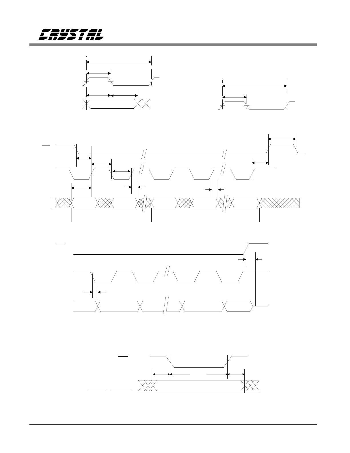
Figure 1. Signal Rise and Fall Characteristics
t
pwl1
tt
su1
t
pw1
t
r
90% 90%
10%
t
pwh1
h1
10%
t
f
EXTENDED
HARDWARE
MODE OR
HOST MODE
(CLKE = 1)
HARDWARE
MODE OR
HOST MODE
(CLKE = 0)
Figure 2. Recovered Clock and Data Switching Characteristics
DS154F2 7
Page 8
TCLK
t
pwh2
t
su2
t
pw2
CS61574A CS61575
t
pw3
t
h2
t
pwh3
TPOS/TNEG
Figure 3a. Transmit Clock and Data Switching
Charact er ist ic s
CS
t
ch
CONTROL BYTE DATA BYTE
t
cl
t
cdh
Figure 4. Serial Port Write Timing Diagram
SCLK
SDI
t
cc
t
dc
LSB LSB
CS
ACLKI
Figure 3b. Alternate External Clock Characteristics
t
cwh
t
cch
t
cdh
MSB
t
cdz
SCLK
t
cdv
SDO
HIGH Z
CLKE = 1
Figure 5. Seria l Port R ead Timi ng Di agra m
PCS
t
h4
LEN0/1/2 , T A OS,
RLOOP, LLOOP,
t
su4
t
pcsl
VALID INPUT DATA
RCODE, TCODE
Figure 6. Exte nded Ha rdwa re Mo de Par allel Chip Select Timin g Dia gram
8 DS154F2
Page 9

CS61574A CS61575
THEORY OF OPERATION
Enhancements in CS61575 and CS61574A
The CS61574A a nd CS61575 provid e high er p erformance and more features than the CS61574
including:
• AT&T 62411, Stratum 4 complian t jitter at-
tenuation over the full rang e of operatin g
frequency and jitte r amplitude (CS6157 5),
• 50% lower power consumption,
• Internally matched trans mitter outpu t im-
pedance for improved signal q uality,
• Optional AMI, B8ZS, HDB3 enc oder/de-
coder or external line coding support,
• Receiver AIS (unframed all ones ) detect ion,
• ANSI T1.231-1993 compliant receiver
LOS (Loss of Signal) handli ng,
• Transmitter TTIP and TRING ou tputs are
forced low when TCLK is static,
• The Driver Performan ce Monitor op erates
over a wider range of input signal levels.
Existing design s using the CS61574 can be converted to th e higher perform ance, pin-co mpatible
CS61574A or CS61575 if the transmit transformer is replaced by a pin-compatible
transformer with a new turns ratio.
Understanding the Difference Between the
CS61575 and CS61 574A
The CS61574A and CS61575 provide receiver
jitter attenuation performance optimized for different appli cations. The CS6 1575 is optimize d to
attenuate l arge amplitud e, low fre quency jitte r for
T1 Customer Prem ises Equi pm ent ( CPE ) app lications as required by AT&T 62411. The
CS61574A is optimized to minimize data delay in
T1 and E1 switching or transmission applications.
Refer to the "Jitter Attenuator" section for additional information.
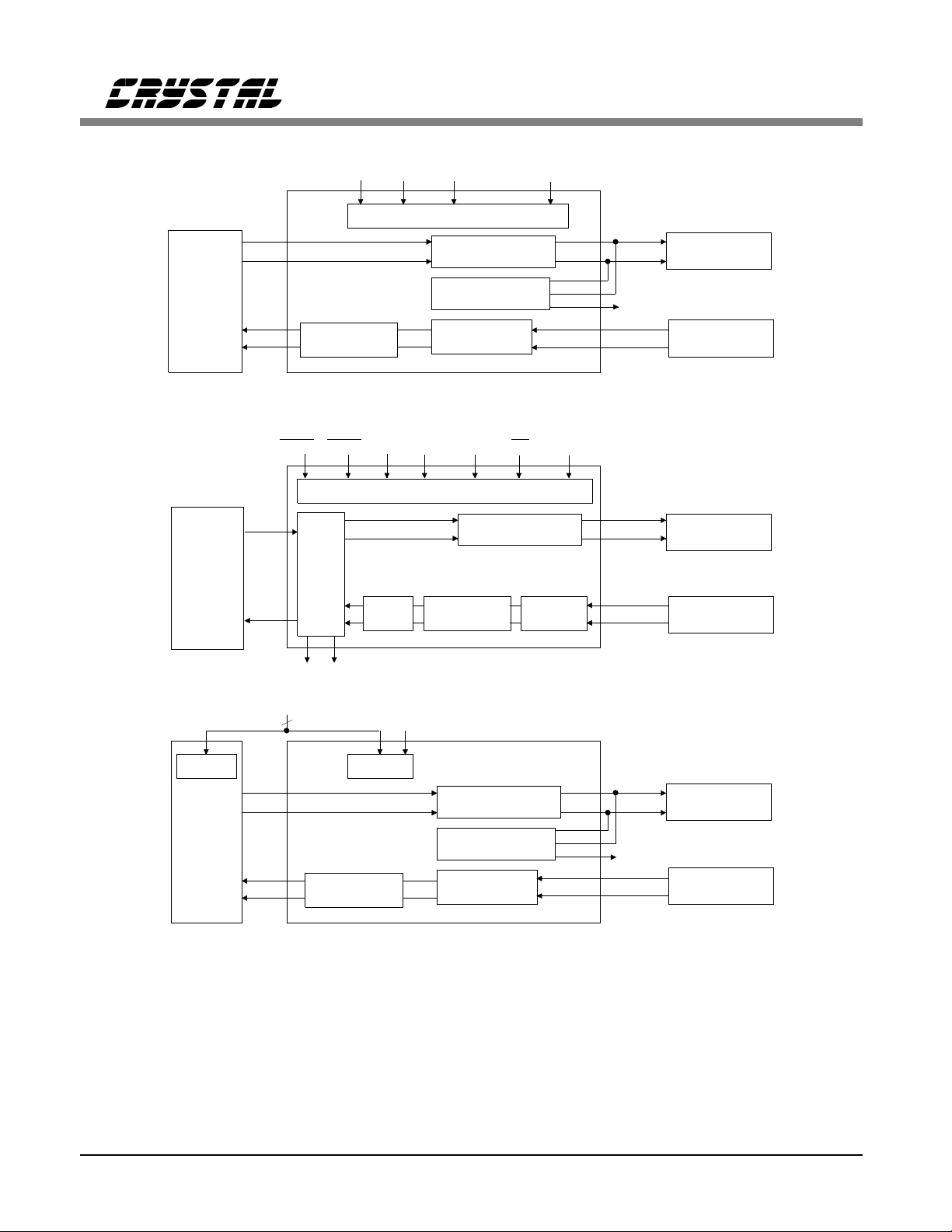
Introduction to Operating Modes
The CS61574A and CS61 575 support three operating modes wh ich are s electe d by th e level of the
MODE pin as shown in Tables 1 and 2, Figure 7,
and Figures A1-A3 of the Applications section.
The modes are Hardware Mode, E xtended Hardware Mode, and Host Mode. In Hardware and
Extended Hardware Modes, discre te pin s are used
to configure and monitor the device. The Extended Hardware Mode provides a parallel chip
select input which latches the control inputs allowing individual ICs to be configured using a
common set of control lines. In the Host Mode,
an external processor monito rs and configures the
device through a serial interface. There are thirteen multi-function pins whose functionality is
determined by the operating mode. (see Table 2).
Hardware
Mode
Control
Method
MODE
Pin
Level
Line
Coding
AIS
Detection
Driver
Performance
Monitor
Table 1. Diff erences Betwe en Operati ng Modes
Control
Pins
<0.2 V Floating or
External Internal-
No Yes No
Yes No Yes
Extended
Hardware
Mode
Control Pins
with Parallel
Chip Select
2.5 V
AMI, B8ZS,
or HDB3
Host
Mode
Serial
Interface
>(R V+)-0.2
V
External
DS154F2 9
Page 10
CS62180B
FRAMER
CIRCUIT
T1 or E1
REPEATER
OR
MUX
TNEG
RPOS
RNEG
TDATA
RDATA
CS61575
CS61574A
JITTER
ATTENUATOR
RCODETCODE
AMI
B8ZS,
HDB3,
CODER
HARDWARE MODE
RLOOP LEN0/1/2LLOOPTAOS
CONTROL
LINE DRIVER
DRIVER MONITOR
LINE RECEIVER
EXTENDED HARDWARE MODE
RLOOP PCS LEN0/1/2LLOOPTAOS
CONTROL
LINE DRIVER
CS61575
CS61574A
AIS
DETECT
JITTER
ATTENUATOR
MRING
MTIP
LINE
RECEIVER
TTIPTPOS
TRING
DPM
RTIP
RRING
TTIP
TRING
RTIP
RRING
CS61574A CS61575
TRANSMIT
TRANSFORMER
RECEIVE
TRANSFORMER
TRANSMIT
TRANSFORMER
RECEIVE
TRANSFORMER
CONTROL
CS62180B
FRAMER
CIRCUIT
BPV AIS
P SERIAL PORT
µ
5
TPOS
TNEG
RPOS
RNEG
HOST MODE
CLKE
CONTROL
LINE DRIVER
CS61575
CS61574A
JITTER
ATTENUATOR
DRIVER MONITOR
LINE RECEIVER
Figure 7. Overv iew of Op eratin g Mode s
MRING
MTIP
TTIP
TRING
DPM
RTIP
RRING
TRANSMIT
TRANSFORMER
RECEIVE
TRANSFORMER
10 DS154F2
Page 11
CS61574A CS61575
MODE
FUNCTION PIN HARDWARE
TRANSMITTER
RECEIVER/ DPM
CONTROL
3TPOS TDATA TPOS
4TNEG
6 RNE G BPV RNEG
7RPOS RDATA RPOS
11 DPM AIS DPM
17 MTIP
18 MRI NG - MRING
18 23 LEN0 LEN0
24 LEN1 LEN1 SDI
25 LEN2 LEN2 SDO
26 RLOOP RLOOP
27 LLOOP LLOOP SCLK
28 TAOS TAOS CLKE
EXTENDED
HARDWARE
TCODE TNEG
RCODE MTIP
PCS -
HOST
INT
CS
Table 2. Pin Definitions
Transmitter
The transmitter takes digita l T1 or E1 input data
and drives appropriately shaped bipolar pulses
onto a transmission line. The transmit data (TPOS
& TNEG or TDATA) is supplied synchronously
and sampled on the falling edge of the input
clock, TCLK.
Either T1 (DSX-1 or Network Interface) or E1
CCITT G.703 pulse shapes may be selected.
Pulse shaping and signal level are controlled by
"line length select" inputs as shown in Table 3.
LEN2 LEN1 LEN0 Option Selected Application
0 1 1 0-133 FEET
1 0 0 133-266 FEET
1 0 1 266-399 FEET
1 1 0 399-533 FEET
1 1 1 533-655 FEET
000
0 0 1 AT&T CB113 Repeater
0 1 0 FCC PART 68, OPT. A Network
011 ANSI T1.403
120Ω (1:1.26)
75Ω (1:1)
Table 3. Line Length Selection
DSX-1
ABAM
(AT&T 600B
or 600C)
E1
CCITT G.703
Interface
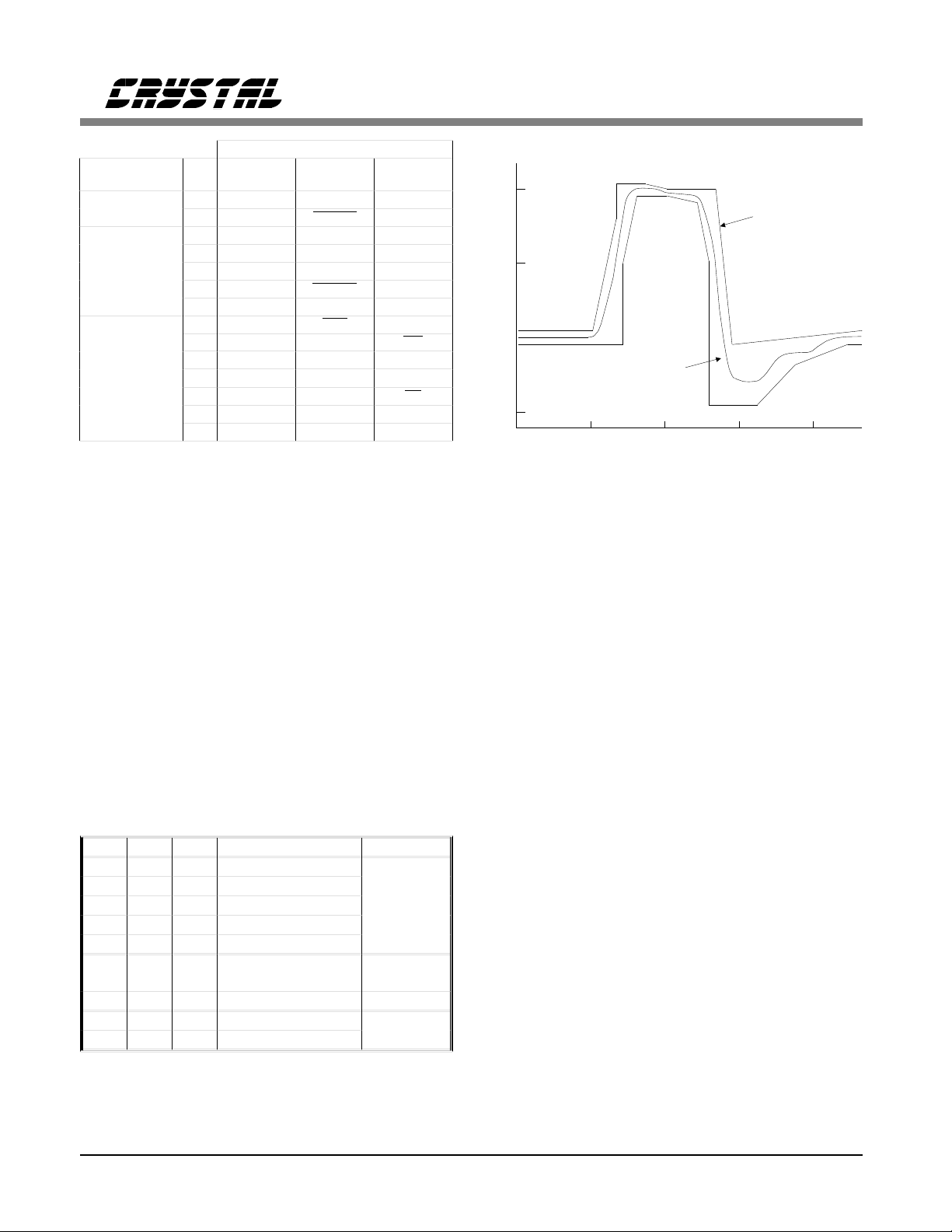
NORMALIZED
AMPLITUDE
1.0
0.5
0
OUTPUT
PULSE SHAPE
-0.5
0 250 750 1000
500
TIME (nanoseconds)
ANSI TI.102,
AT&T CB 119
SPECIFICATIONS
Figure 8. Typical Pulse Shape at DSX-1 Cross Connect
The CS61575 and CS6157 4A line drivers are designed to drive a 75 Ω equivalent load.
For E1 applicatio ns, t he C S615 74A a nd CS615 75
drivers provide 14 dB of return loss during the
transm ission o f both mark s and sp aces. This i mproves signal quality by minimizing reflections
off the transmitter. Similar levels of return loss
are provided for T1 applications.
For T1 DSX-1 applications, line len gths from 0 to
655 feet (as measured from the transmitter to the
DSX-1 cross connect ) may be selected. The five
partition arrangement in Table 3 meets ANSI
T1.102 and AT&T CB-119 requirements when
using #22 ABAM cable. A ty pical outp ut puls e is
shown in Figu re 8. These pulse s ettings can also
be used to meet CCITT puls e shape requi rements
for 1.544 MHz operation.
For T1 Network Interface applications , two additional opt ions are pr ovided. Note t hat the opt imal
pulse width for Part 68 (32 4 ns) is narrower than
the optimal puls e width for DSX-1 (350 ns). T he
CS61575 and CS61574A automatically adjusts
the pulse width based upon the "lin e length" selection made.
DS154F2 11
Page 12
CS61574A CS61575
Percent of
nominal
peak
voltage
120
110
100
90
80
50
10
0
-10
-20
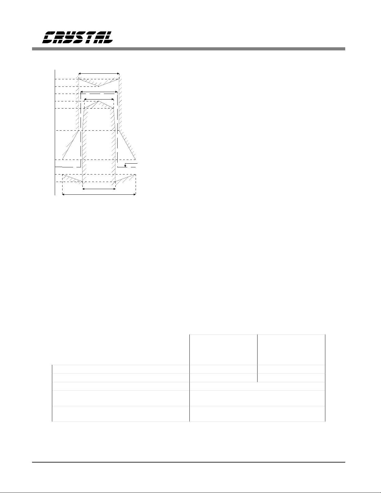
Figure 9. Mask of the Pulse at the 2048 kbps Interface
269 ns
244 ns
194 ns
Nominal Pulse
219 ns
488 ns
The E1 G.703 pu lse shape is supported wit h line
length selection LEN2/1/0=0/0/0. The pulse
width will meet the G.703 pulse shape template
shown in Figure 9, and specified in Table 4.
The CS61574A an d CS61575 will detect a static
TCLK, and will force TTIP and TRING low to
prevent transmission when data is not present.
When any transmit control pin (TAOS, LEN0-2
or LLOOP) is toggled, the transmitter outputs
will require appro ximat ely 22 bi t pe riod s to stab ilize. The transmitter will take longer to stabilize
when RLOOP is select ed because the timing circuitry must adjust to the new frequency.
Transmit All On es Select
The transmitte r provides for all ones insertion at
the frequency of TCLK. Transmit all ones is selected when TAOS goes high, and causes
continuous ones to be transmitted on the line
(TTIP and TRING). In this mode, the TPOS and
TNEG (or TDATA) inputs are ignored. If Remote
Loopback i s in effect, any TAOS request will be
ignored.
Receiver
The receiver extracts dat a an d cl ock fro m an AMI
(Alternate Mark Inversion) coded signal and outputs clock an d synchronized data. The receiver is
sensitive to signals over the entire range of
ABAM cable lengths and requires no equalizati on
or ALBO (Automatic Line Build Out) circuits.
The signal is received on both ends of a centertapped, center-grounded transformer. The
transformer is center tapped on the IC side. The
clock and dat a recovery circuit exceeds the jitter
tolerance specifications of Publications 43802,
43801, AT&T 62411, TR-TSY-000170, and
CCITT REC. G.823.
For coaxial cable,
75Ω load and
transformer specified
in Application Section.
Nominal peak voltage of a mark (puls e) 2.37 V 3 V
Pea k voltage of a space (no pulse)
Nominal puls e wi dt h 244 ns
Ratio of the amplitudes of positive and negative
pulses at the center of the pulse interval
Ratio of the widths of positive and negative
pulses at the nomi nal half amplitude
* When configured with a 0.47 µF nonpolarized capacitor in series with the TX transformer
primary as shown in Figures A1, A2 and A3.
Table 4. CCITT G.703 S pecificati ons
12 DS154F2
0 ±0.237 V 0 ±0.30 V
0.95 to 1.05*
0.95 to 1.05*
For shielded twisted
pair, 120Ω load and
transformer specified
in Application Section.
Page 13
CS61574A CS61575
RTIP
1 : 2
RRING
Data
Level
Slicer
Edge
Detector
Figure 1 0. Re cei ver Bl oc k Di agr am
A block diagram of the rece iver is shown in Figure 10. The two leads of the transformer (RTIP
and RRING) have opp osite polarity allowing th e
receiver to treat RTIP and RRING as unipolar signals. Comparators are used to detect pulses on
RTIP and RR ING. The compar ator thre shold s are
dynamically established at a percent of the peak
level (50% of peak for E1, 65% of peak for T1;
with the slicing level selected by LEN2/1/0 inputs).
The leading edge of an incoming data pulse triggers the clock ph ase selector. The phase selector
chooses one of t he 13 available phases which th e
delay line pro duces for each bit perio d. The output from the phase selector feeds the clock and
data recovery circuits which generate the recovered clock and sample the incoming signal at
appropriate intervals to recover the data.
Data sampling will continue at the periods selected by the phase selector until an incoming
pulse deviates enou gh to cause a new phase to be
selected for da ta sampling. The phases of the d elay line are selected and updated to allow as much
as 0.4 UI of jitter from 10 kHz to 100 kHz, without error. The jitter tolerance of the receiver
exceeds that shown in Figure 11. Additionally,
this method o f clock and d ata recovery is tol erant
of long strings of consecutive zeros. The data
Data
Sampling
& Clock
Extraction
Clock
Phase
Selector
Continuously
Calibrated
Delay Line
Jitter
Attenuator
RPOS
RNEG
RCLK
sampler will continuously sample data based on
its last input until a new pulse arrives to update
the clock phase selector.
The delay line is continuously calibrated using
the crystal oscillator reference clock. The delay
line produces 13 phases for eac h cycle of the reference clock. In effect, the 13 phases are
analogous to a 20 MHz clock when the reference
clock is 1.544 MHz. This implementation utilizes
the benefits of a 2 0 MHz clo ck for cl ock recovery
without actually having the clock present to impede analog circuit performance.
Minimum
300
138
PEAK-TO-PEAK
JITTER
(unit intervals)
100
28
10
1
.4
.1
AT&T 62 411
Figure 11. Minimum Inpu t Jitter Tole rance of R eceiver
Performance
10
JITT E R F R E QUENC Y (Hz)
300
1k
10k1 100 100k700
DS154F2 13
Page 14
CS61574A CS61575
In the Hardware Mode, da ta at RPOS and RNEG
should be sampled on the rising edge of RCLK,
the recovered clock. In the Extended Hardware
Mode, data at RDATA should be sampled on th e
falling edge o f RCLK. In the Host Mode , CLKE
determines the clock polarity for which output
data should be sampled as shown in Table 5.
MODE
(pin 5)
LOW
(<0.2V)
HIGH
(>(V+) - 0.2V)
HIGH
(>(V+) - 0.2V)
MIDDLE
(2.5V)
X = Don’t care
Table 5. Data Ou tput/Clock Relatio nship
CLKE
(pin 28)
XRPOS
LOW RPOS
HIGH RPOS
X RDATA RCLK Falling
DATA CLOCK Clock Edge
for V alid Data
RCLK
RNEG
RNEG
SDO
RNEG
SDO
RCLK
RCLK
RCLK
SCLK
RCLK
RCLK
SCLK
Rising
Rising
Rising
Rising
Falling
Falling
Falling
Rising
Loss of Signal
The receiver will indicate loss of signal after
power-up, reset or upon receiving 175 consecutive zeros. A digital counter counts received
zeros, base d on RCLK cycles. A zero is received
when the RTIP and RRING inputs are below the
input comparator slicing threshold level established by the peak detector. After the signal is
removed for a period of time the data slicing
threshold level decays to approximately
300 mV
peak
.
If ACLKI is present during the LOS state, ACLKI
is switched int o the input of the jitter attenua tor,
resulting in RCLK matching the frequency of
ACLKI. The jitter attenuator buffers any inst antaneous changes in phase between the last
recovered clock and the ACLKI reference clock.
This means that RCLK will smoothly transition
to the new frequency. If ACLKI is not present,
then the crys tal os cil lator of t he j itter atten uat or is
forced t o its center frequ ency. Ta ble 6 shows the
status of RCLK upon LOS.
Crystal
present?
No Yes ACLKI
Yes No Centered Crystal
Yes Yes
ACLKI
present?
Table 6. RC LK Stat us at L OS
Source of RCLK
ACLKI via the
Jitter Attenuator
Jitter Attenuator
The jitter at tenuator reduces wander and jitte r in
the recovered clock si gnal. It consists of a 32 or
192-bit FIFO, a crystal oscillator, a set of load
capacitors for the crystal, and control logic. The
jitter attenuator exceeds the jitter attenuation requirements of Publications 43802 and REC.
G.742. A typi cal jitter a ttenuation cu rve is shown
in Figure 12. The CS61575 fully meets AT&T
62411 jitter attenuation requirements. The
CS61574A will have a discontinuity in the jitter
transfer function whe n the incoming jitter amplitude exceeds approximately 23 UIs.
The jitter attenu ator works in the following manner. The recovered clock and data are in put to t he
FIFO with the recovered clock controlling the
FIFO’s write pointer. The crystal oscillator controls the FIFO’s read pointer which reads data out
of the FIFO and presents it at RPOS and RNEG
(or RDATA). RCLK is equivalent to the oscillator’s output. By changing the load capacitance
that the IC presents to the crystal, the oscillatior
frequency (and RCLK) is a djusted to the average
frequency of the recovered signal. Logic determines the phase relationship between the read and
write pointe rs and decid es how to adjust the lo ad
capacitance o f th e c rystal . Jitte r is ab so rbed in the
FIFO accordi ng to t he jitt er tra nsfer ch aracteri stic
shown in Figure 12.
14 DS154F2
Page 15

CS61574A CS61575
0
10
20
30
40
b) Maximum
Attenuation
Attenuation in dB
Limit
50
60
1 10 100 1 k 10 k
Figure 12. Typ ical Jitte r Tr ansf er Fun ction
a) Minimum Attenuation Limit
62411 Requireme nts
Measured Perf ormanc e
Frequency in Hz
The FIFO in the jitter attenuator is designed to
prevent overflow and underflow. If the jitter amplitude becomes very large, the read and write
pointers may get very clos e together. Should they
attempt to cross, the oscillator’s divide by four
circuit adjusts by performing a divide by 3 1/2 or
divide by 4 1/2 to prevent the overflow or underflow. During this activity, data will never be lost.
The difference between the CS61575 and
CS61574A is the depth of the FIFO in the jitter
attenuator. The CS61575 has a 192-bit FIFO
which allows it to atten uate large amplitude, low
frequency jitter as req uire d by AT&T 62411 (e.g .,
28 UIpp @ 300 Hz). This makes the CS61575
ideal for use in T1 Customer Premises Equipment
which must be compatible wit h AT&T 62411 requirements. In single-line Stratum 4, Type II
systems which are loop-timed, he CS61575 recovered clock can be used as the transmit clock
eliminating the need for an exte rnal system c lock
synchronizer. In Stratum 4, Type I systems which
transfer timing and re quire a clock synchronizer,
the CS61575 simplifies the design of the synchronizer by absorb ing large ampl itude low frequency
jitter before it reaches the synchronizer.
The CS61574A has a 32-b it FIFO whic h allows it
to absorb jitter with minimum data delay in T1
and E1 switching or transmission applications.
The CS61574A will tolerate large amplitu de jitter
by tracking rather than attenuating it, preventing
data errors so that the jitter may be absorbed in
external frame buffers. With large amplitude input
jitter, the CS61574A jitter transfer function may
exhibit some jitter peaking, but will offer performance comparable to the CS61574.
The jitter a ttenuator may be bypassed by pulling
XTAL IN to RV+ through a 1 kΩ resistor and pro-
viding a 1.544 MHz (or 2.048 MHz) clock on
ACLKI. RCLK may exhibit quantiz ation jitter of
approximately 1/13 UIpp and a duty cycle of approximately 30% (70%) when the attenuator is
disabled.
Local Loopback
Local loopbac k is selected by taking LLOOP, pin
27, high or by setting the LLOOP register bit via
the serial interface.
The local loopback mode takes clock and data
presented on TCLK, TPOS, and TNEG (or
TDATA), send s it thro ugh th e jitt er a ttenua tor a nd
outputs it at RCLK, RPOS and RNEG (or
RDATA). If the jitter attenuator is disabled, it is
bypassed. Inputs to the tr ansmitter are still transmitted on TTIP and TRING, unless TAOS has
been selec ted in which case, AMI-coded conti nuous ones are tra nsmitted at the TCLK freq uency.
The receiver RTIP and RRING inp uts are i gnored
when local loopback is in effect.
DS154F2 15
Page 16

CS61574A CS61575
Remote Loopba ck
Remote loopback is selected by taking RLOOP,
pin 26, high or b y setting the RLOOP register bit
via the serial interface.
In remote loopback , the recovered clock and data
input on RTIP and RRING are sent through the
jitter attenuator an d back out on the line via TTIP
and TRING. Sel ecting remote loop back overrides
any TAOS request (see Table 7). The recovered
incoming signals are also sent to RCLK, RPOS
and RNEG (or RDATA). Simultaneous selec tion
of local and remot e loopback modes is not valid
(see Reset).
RLOOP
Input
Signal
Notes: 1. X = Don’t care. The identified All Ones Select
TAOS
Input
Signal
00 TDATA TCLK
0 1 all 1s TCLK
1 X RTIP & RRING RTIP & RRING (RCLK)
input is ignored when the indicated loopback
is in effect.
2. Logic 1 indicates that Loopback or All Ones
option is selected.
Table 7. Intera ctio n of RLOOP with TAOS
Source of
Data for
TTIP & TRING
Source of
Clock for
TTIP & TRING
In the Extended Hardware Mode the transmitted
data is looped before the AMI/B8ZS/HDB3 encoder/decoder du ring remot e loopbac k so that th e
transmitted signal matches the received signal,
even in the presence of received bipolar violations. Data output on RDATA is decoded,
however, if
RCODE is low.
Driver Performance Monitor
To aid in early detection and easy isolation of
non-functioning links, the IC is able to monitor
transmit drive performance and report when the
driver is no longer operational. This feature can
be used to monitor either the device’s performance or th e performance of a neigh boring driver.
The driver performance monitor indicat or is nor-
mally low, and goes high upon de tecting a driver
failure.
The driver performance monitor consists of an activity detector th at mo nito rs t he t ransm itt ed sign al
when MTIP is connected to TT IP and MRING is
connected to TRING. DPM will go high if the
absolute difference between MTIP and MRING
does not transition above or below a threshold
level within a time-out period. In the Host Mode,
DPM is available from both the register and pin
11.
Whenever more than on e line interface IC res ides
on the sa me ci rcuit bo ard, th e effectiveness of the
driver performance monitor can be maxi mized by
having each IC monitor perfo rmance of a neighboring IC, rather than having it monitor its own
performance. Note that a CS61574A or C S61575
can not be used to monit or a CS61 574 due to output stage differences.
Line Code Encode r/Decoder
In the Extended Hardware Mod e, three line code s
are available: AMI, B8ZS and HDB3. The inp ut
to the encoder is TDATA. The outputs from the
decoder are RDATA and BPV (Bipolar Violation
Strobe). The encoder and decoder are selected
using the LEN2, LEN1, LEN0,
TCODE and
RCODE pins as shown in Table 8.
LEN 2/1/0
000 010-111
TCODE
(Transmit
Encoder
Selection)
RCODE
(Receiver
Decoder
Selection)
LOW
HIGH
LOW
HIGH
Table 8. En code r/Deco der S elect ion
HDB3
Encoder
HDB3
Decoder
B8ZS
Encoder
AMI
Encoder
B8ZS
Decoder
AMI
Decoder
16 DS154F2
Page 17

CS61574A CS61575
Alarm Indication Signal
In the Extended Hardware Mode, the receiver sets
the output pin AIS high when less than 9 zeros
are detected ou t of 8192 bit periods. AIS retu rns
low when 9 or more zeros are detected out of
8192 bit periods.
Parallel Chip Se lect
In the Extended Hardware Mode,
used to gate the digital control inputs:
PCS can be
TCODE,
RCODE, LEN0, LEN1 , LEN2, RLOOP, LLOOP
and TAOS. Inputs are accept ed on these pi ns only
when
PCS is low and will immediately change
the operating state of th e device. There fore, when
cycling
PCS to update the operating state, the
digital control i nputs should be stable for the entire
PCS low period. The digital control inputs are
ignored when
PCS is high.
Power On Reset / Reset
Upon power-up, the IC is held in a static state
until the supply crosses a threshold of approximately 3 Volts. When this threshold is crossed,
the device will delay for about 10 ms to allow the
power supply to reach operating voltage. After
this delay, calibration of the delay lines used in
the transmit and receive sections commences . The
delay lines can be calibrated only if a reference
clock is present. The reference clock for the receiver is provided by the crystal oscillator, or
ACLKI if the oscillator is disable d. The refe rence
clock for the transmitter is provided by TCLK.
The initial calibration should take less than
20 ms.
In operation, the delay lines are continuously cal ibrated, making the performance of the device
independent of power supply or t emperature variations. The continuous calibration function
forgoes any requirem en t to re set the l ine inte rface
when in operation. However, a reset function is
available which will clear all registers.
In the Hardware and Extended Hardware Modes,
a reset request is ma de by simultaneously se tting
both the RLOOP and LLOOP pins high for at
least 200 ns. Reset will initiate on the falling edge
of the reset reque st (falling edg e of RLOOP and
LLOOP). In the Host Mo de, a res et is initia ted by
simultaneously writing RLOOP and LLOOP to
the register. In either mode, a reset will set all registers to 0 and force the oscillator to its center
frequency before initiating calibration. A reset
will also set LOS high.
Seria l Inte rfa ce
In the Host Mode, pins 23 t hrough 28 serve as a
microprocessor/microcontroller interface. One
on-board register can be written to via the SDI
pin or read from via the SDO pin at t he cl ock ra te
determined by SCLK. Through this register, a
host controller can be used to con trol operational
characteris tics and monitor device s tatus. The s erial port read/write timing is independent of the
system transmit and receive timing.
Data transfer s are initiated by ta king the chip select input,
CS, low (CS must initially be high).
Address and i nput data bits are c locked in on the
rising edge of SCLK. The clock edge on which
output data is stable and valid is determined by
CLKE as shown in Table 5. Data transfers are terminated by setting
CS high. CS may go high no
sooner than 50 ns after the rising edge of the
SCLK cycle corresponding to the last write bit.
For a serial data read,
CS may go hig h any time
to terminate the output.
Figure 13 shows the timing rel ationships for data
transfers whe n CLKE = 1. When CLKE = 1, da ta
bit D7 is held until the falling edge of the 16th
clock cycle. When CLKE = 0, da ta bit D7 is he ld
until the rising ed ge of the 17th clock cycle. SDO
goes High-Z a fter
CS goes high or at the end of
the hold period of data bit D7.
DS154F2 17
Page 18

CS
SCLK
CS61574A CS61575
SDI
SDO
R/W
0
0
Address/Command Byte
00 01 0
Figure 13. Input/Output Timing
An address/command byte, shown in T able 9, precedes a data register. The first bit of the
address/comman d b yte deter min es whe the r a rea d
or a write is request ed. The next six bits contain
the address. The line interface responds to address
16 (0010000). The last bit is ignored.
LSB, first bit 0 R/W Read/Write Select; 0 = write, 1 = read
1 ADDP LSB of address, Must be 0
2 ADD1 Must be 0
3 ADD2 Must be 0
4 ADD3 Must be 0
5 ADD4 Must be 1
6 - Reserved - Must be 0
MSB, last bit 7 X Don’t Care
Table 9. Add ress/Co mmand Byte
The data regis ter, shown in Table 10, can be written to the serial port. Data is input on the eight
clock cycles immediately following the address/command byte. Bits 0 and 1 are used to
clear an interrup t issued from the
INT pin, which
occurs in response to a loss of signal or a problem
with the output driver.
D7D6D5D4D3D2D1D0
Data Inpu t/ Ou tput
D6D5D4D3D2D1D0 D7
Writing a "1" to either "Clear LOS" or "Clear
DPM" over the serial interface has three effects:
1) The current interrupt on the serial interface
will be cleared. (Note that simply reading
the register bits wi ll not clear the interrupt).
2) Output data bits 5, 6 and 7 will be reset as
appropriate.
3) Future interrupts for the correspondi ng LOS
or DPM will be prevented from occurring.
Writing a "0" to either "Clear LOS" or "Clear
DPM" enables the corresponding interrupt for
LOS or DPM.
Output data from the se rial interface is pr esented
as shown in Tables 11 and 12. Bit s 2, 3 and 4 can
be read to verify line length selection. Bits 5, 6
and 7 must be decoded. Cod es 101, 110 and 111
(Bits 5, 6 and 7) indicate intermittent lo ss of signal and/or driver problems.
SDO goes to a high i mpedance state when not in
use. SDO and SDI may be tied tog ether in applications where the host processor has a
bi-directional I/O po rt.
LSB, first bit 0 clr LOS Clear Loss Of Signal
in 1 clr DPM Clear Driver Performance
2 LEN0 Bit 0 - Line Length S elect
3 LEN1 Bit 1 - Line Length S elect
4 LEN2 Bit 2 - Line Length S elect
5 RLOOP Remote Loopback
6 LLOOP Local Loopback
MSB, last bitin7 TAOS Transmit All Ones Select
Table 10. Input Data Register
18 DS154F2
LSB, fi rst bit 0 LOS Loss Of Signal
in 1 DPM Driver Performance
2 LEN0 Bit 0 - Line Lengt h Select
3 LEN1 Bit 1 - Line Lengt h Select
4 LEN2 Bit 2 - Line Lengt h Select
Table 11. Output Da ta Bi ts 0 - 4
Page 19

Bits Status
567
0 0 0 Reset has occurred or no program input.
001TAOS in effect.
0 1 0 LLOOP in effect
0 1 1 TAO S/LLO OP in eff e ct.
1 0 0 RLOOP in effect.
1 0 1 DPM changed state since last "clear DPM"
occurred.
1 1 0 LOS changed state since last "clear LOS"
occurred.
1 1 1 LOS and DPM have changed state since
last "clear LOS" and "clear DPM".
Table 12. Coding for Serial Output bits 5,6,7
Power Supply
The device operates from a si ngle +5 Volt supply.
Separate pins for transmit and receive supplies
provide internal isolation. These pins should be
connected externally near the device and decoupled to their respective grounds. TV+ must not
exceed R V+ by more than 0.3V.
CS61574A CS61575
Schematic & Layout Review Service
Confirm Optimum
Schematic & Layout
Before Building Your Board.
For Our Free Review Service
Call Applications Engineering.
Call:(512) 445-7222
Decoupling an d filtering of the power supplies is
crucial for the proper opera tion of the analog circuits in both th e transmit and rece ive paths. A 1.0
µF capacitor should be connected between TV+
and TGND, and a 0.1 µF capacitor should be con-
nected between RV+ and RGND. Use mylar or
ceramic capacitors and place them as closely as
possible to the ir respective power supply pins. A
68 µF tantalum capacitor should be added close
to the RV+/RGND supply. Wire-wrap breadboarding o f the line interface is not recommended
because lead resistance and inductance serve to
defeat the function of the decoupling capacitors.
DS154F2 19
Page 20

PIN DESCRIPTIONS
CS61574A CS61575
Hardware Mode
ACLKI TAOS
TCLK LLOOP
TPOS RLOOP
TNEG L EN 2
MODE LEN1
RNEG LEN0
RPOS RGND
RCLK RV+
XTALIN RRING
XTALOUT RTIP
DPM MRING
LOS MT IP
TTIP TRING
TGND T V+
1
2
3
4
5
6
7
8
9
10
11
12
13
14
ACLKI
28
27
26
25
24
23
22
21
20
19
18
17
16
15
TCLK TAOS
TPOS LLOOP
TNEG RLOOP
MODE LEN2
327242628
RNEG LEN1
RPOS LEN0
RCLK RGND
XTALIN RV+
XTALOUT RRING
5
6
7
8
9
10
11
12 14 16 18
1
top
view
13 15
25
24
23
22
21
20
19
17
DPM RTIP
LOS MRING
TTIP MTIP
TGND T RI NG
TV+
20 DS154F2
Page 21

Extended Hardware M ode
CS61574A CS61575
ACLKI TAOS
TCLK LLOOP
TDATA RLOOP
TCODE LEN2
MODE LEN1
BPV LEN0
RDATA RGND
RCLK RV+
XTALIN RRING
XTALOUT RTIP
LOS
TTIP TRING
TGND T V+
AIS
1
2
3
4
5
6
7
8
9
10
11
12
13
14
ACLKI
28
27
26
25
24
23
22
21
20
19
18
17
16
15
PCS
RCODE
TCLK TAOS
TDATA LLOOP
TCODE RLOOP
MODE LEN2
327242628
BPV LEN1
RDATA LEN0
RCLK RGND
XTALIN RV+
XTALOUT RRING
5
6
7
8
9
10
11
12 14 16 18
1
top
view
13 15
25
24
23
22
21
20
19
17
AIS RTIP
LOS
TTIP
PCS
RCODE
TGND T RI NG
TV+
DS154F2 21
Page 22

Host Mode
CS61574A CS61575
ACLKI CLKE
TCLK SCLK
TPOS
TNEG SDO
MODE SDI
RNEG
RPOS RGND
RCLK RV+
XTALIN RRING
XTALOUT RTIP
DPM MRING
LOS MT IP
TTIP TRING
TGND T V+
1
2
3
4
5
6
7
8
9
10
11
12
13
14
ACLKI
28
27
26
25
24
23
22
21
20
19
18
17
16
15
CS
INT
TCLK CLKE
TPOS S CL K
TNEG
CS
MODE SDO
327242628
RNEG SDI
RPOS
RCLK RGND
XTALIN RV+
XTALOUT RRING
5
6
7
8
9
10
11
12 14 16 18
1
top
view
13 15
17
25
24
23
22
21
20
19
INT
DPM RTIP
LOS MRING
TTIP MTIP
TGND T RI NG
TV+
22 DS154F2
Page 23

Power Supplies
RGND - Ground, Pin 22.
Power supply ground for all subcircuits except the transmit driver; typically 0 Volts.
RV+ - Power Supply, Pin 21.
Power supply for all subcircuits except the transmit driver; typically +5 Volts.
TGND - Ground, Transmit Driver, Pin 14.
Power supply ground for the transmit driver; typically 0 Volts.
TV+ - Power Supply, Transmit Driver, Pin 15.
Power supply for the transmit driver; typically +5 Volts. TV+ must not exce ed RV+ by more than
0.3 V.
Oscillator
XTALIN, XTALOUT - Crystal Connecti ons, Pins 9 and 10.
A 6.176 MHz (o r 8.19 2 MHz ) cry stal shoul d be c onn ected acro ss t hese pin s. If a 1.5 44 MHz (or
2.048 MHz) clock is provided on ACLKI (pin 1), the jitter att enuator may be disabled by tyin g
XTALIN, Pin 9 to RV+ through a 1 kΩ resistor, and floating XTALOUT, Pin 10.
Overdriving the oscillator with an external clock is not supported.
CS61574A CS61575
Control
ACLKI - Alternate External Clock Input, Pin 1.
A 1.544 MHz (or 2.048 MHz) clock may be input to ACLKI, or this pin must be tied to ground.
During LOS, the ACLKI input signal, if present, is output on RCLK through the jitter attenuator.
CLKE - Clock Edge, Pin 28 . (Host Mode)
Setting CLKE to logic 1 causes RPOS and RNE G to be valid on t he falling e dge of RCLK, and
SDO to be valid on the risin g edge of SCL K. Conversely, setting CLKE to lo gic 0 causes RPOS
and RNEG to be valid on the rising edge of RCLK, and SDO to be valid on the falling edge of
SCLK.
CS - Chip Select, Pin 26. (Host Mode)
This pin must transition from high to low to read or write the serial port.
INT - Receive Alarm Interrupt, Pin 23. (Host Mode)
Goes low when LOS or DPM change s tate to flag the host proces sor.
"clear LOS" or " clea r DP M" t o t he regist er.
INT is an open drain out put and s hou ld be ti ed t o the
power supply through a resistor.
INT is cleared by writing
DS154F2 23
Page 24

CS61574A CS61575
LEN0, LEN1, LEN2 - Line Length Selection, Pins 23, 24 and 25. (Hardware and Extended
Hardware Modes)
Determines the shape and amplitu de of the tran smitted pulse to acco mmodate several cable types
and lengths. See Table 3 for information on line length selection. Also controls the receiver
slicing level and the line code in Extended Hardware Mode.
LLOOP - Local Loopback, Pin 27. (Hardware and Extended Hardware Modes)
Setting LL OOP to a logic 1 rou tes the transmit clock and d ata throug h the jitter attenu ator to the
receive clock and data pins. TCLK and TPOS/TNEG (or TDATA) are still transmitted unless
overridden by a TA OS request. Inputs on RTIP and RRING are ignored.
MODE - Mode Select, Pin 5.
Driving the MODE pin hi gh puts the lin e interface in the Ho st Mode. In the host mod e, a serial
control por t is used to co ntrol the line i nterface and determi ne its status. Grou nding the MODE
pin puts the line inte rface in the Hardware Mode, where configurati on and status are controlled
by discrete pi ns. Floating the MODE pin or driving i t to +2.5 Vselects the Ext ended Hardware
Mode, where configuration and status are controlled by discrete pins. When floating MODE,
there should be no externa l load on the pin. MODE defines the status of 13 pins (see Table 2).
PCS - Parallel Chip Select, Pin 18. (Extended Hardware Mode)
Setting
PCS high causes the l ine interface to ig nore th e TCODE, RCODE, LEN0, LEN1, LEN2,
RLOOP, LLOOP and TA OS inputs.
RCODE - Receiver Decoder Select, Pin 17. (Extended Hardware Mode)
Setting
RCODE low enables B8ZS or HDB3 zero substitution in the receiver decoder. Setting
RCODE high enables the AMI receiver decoder (see Table 8).
RLOOP - Remote Loopback, Pin 26. (Hardware and Extended Hardware Modes)
Setting RLOOP to a logic 1 causes the recovered clock and data to be sent through the jitter
attenuator ( if active) and through the driver back to the line. The recovered sign al is also sent to
RCLK and RPOS/RNEG (or RDATA). Any TAOS request is ignored.
Simultaneously taking RLOOP and LLOOP high for at least 200 ns initiates a device reset.
SCLK - Serial Clock, Pin 27. (Host Mode)
Clock used to read or write the serial port registers. SCLK can be either high or low when the line
interface is selected using the
CS pin.
SDI - Serial Data Input, Pin 24. (Host Mode)
Data for the on-chip register. Sampled on the rising edge of SCLK.
SDO - Serial Data Output, Pin 25. (Host Mode)
Status and contro l information from the on-chip register. If CLKE is high SDO is valid on the
rising edge of SCLK. If CLKE is low SDO is valid on the falling edge of SCLK. This pin goes to
a high-impedance sta te when the serial port is bein g written to or after bit D7 is output.
24 DS154F2
Page 25

CS61574A CS61575
TAOS - Tra nsmit All Ones Select, Pin 28. (Hardware and Extended Hardware Modes)
Setting TAOS to a logic 1 ca uses continuou s ones to be transmitted at th e frequency determined
by TCLK.
TCODE - Transmitter Encoder Select, Pin 4. (Extended Hardware Mode)
Setting
TCODE low enables B8ZS or HDB3 zero substi tution in the transmitter encode r. Setting
TCODE high enables the AMI transmitter encoder .
Data
RCLK - Recovered Clock, Pin 8.
The receiver recovered clock ge nerated by the j itter attenua tor is output o n this pin.When i n the
loss of signal state ACLKI (if present) is output on RCLK via the jitter attenuator. If ACLKI is
not present during LOS, RCLK is forced to the center frequency of the crystal oscillator..
RDATA - Receive Data - Pin 7. (Extended Hardware Mode)
Data recovered from the RTIP and RRING inputs is outpu t at this p in, afte r bein g decode d by th e
line code decoder. RDATA is NRZ. RDATA is stable and valid on the falling edge of RCLK.
RPOS, RNEG - Receive Positive Data, Receive Negative Data, Pins 6 and 7 . (Hardware and Host
Modes)
The receiver recovered NRZ digital data is output on these pins. In the Hardware Mode, RPOS
and RNEG are stable and valid on the rising edge of RCLK. In the Host Mode, CLKE determines
the clock edge for which RPOS and RNEG are stable and valid. See Table 5. A positive pulse
(with respect to gro und) received on the RTIP pin generates a logic 1 on RPOS, and a positive
pulse received on the RRING pin generates a logic 1 on RNEG.
RTIP, RRING - Receive Tip, Receive Ring , Pins 19 and 20.
The AMI receive signal is input to these pins. A center-tapped, center-grounded, 2:1, step-up
transformer is require d on these inputs, as shown in Figure A1 in the Appl ications secti on. Data
and clock are recovered and output on RCLK and RPOS/RNEG or RDATA.
TCLK - Tr ansmit Clock, Pin 2.
The1.544 MHz (o r 2.048 MHz) trans mit clock is input on this pin. TPOS/TNEG or TDATA are
sampled on the falling edge of TCLK.
TDATA - Transmit Data, Pin 3. (Extended Hardware Mode)
Transmitter NRZ input d ata which passes th rough the li ne code encoder, and is then driven on to
the line through TTIP and TRING. TDATA is sampled on the falling edge of TCLK.
TPOS, TNEG - Transmit Positive Data, Transmit Negative Data, Pins 3 and 4. (Hardware and
Host Modes)
Inputs for clock and data to be transmi tted. The signal is driven on to the l ine through TT IP and
TRING. TPOS and TNEG are sampled on the falling edge of TCLK. A TPOS input causes a
positive pulse to be transmitted, while a TNEG input causes a negative pulse to be transmitted.
DS154F2 25
Page 26

TTIP, TRING - Transmit Tip, Transmit Ring, Pins 13 and 16.
The AMI signal is driven to the line t hrough these pins. The tr ansmitter output is d esigned to
dri ve a 75 Ω load between TT IP and TR ING. A tran sformer is required a s shown in Table A1.
Status
AIS - Alarm Indication Signal, Pin 11. (Extended Hardware Mode)
AIS goes high when unframed all-ones condition (blue alarm) is detected, using the detection
criteria of less than three zeros out of 2048 bit periods.
BPV- Bipolar Violation Strobe, Pin 6. (Extended Hardware Mode)
BPV strobes high when a bipolar violation is detected in the received signal. B8ZS (or HDB3)
zero su bstituti ons ar e not flag ged as bi polar vi olatio ns if th e B8ZS (or H DB3) dec oder has be en
enabled.
DPM - Driver Performance Monitor, Pin 11. (Hardware and Host Modes)
DPM goes high if no activity is detected on MTIP and MRING.
LOS - Loss of Signal, Pin 12.
LOS goes high when 175 consecutive zeros have been received. LOS returns low when the ones
density reache s 12.5% (based u pon 175 bit peri ods starting with a one and co ntaining less tha n
100 consectutive zeros) as prescribed in ANSI T1.231-1993. When in the loss of signal state
RPOS/RNEG or RDATA are forced low, and ACLKI (if present) is output on RCLK via the jitter
attenuator. If ACLKI is not present during LOS, RCLK is forced to the center frequency of the
crystal os cillator.
CS61574A CS61575
MTIP, MRING - Monitor Tip, Monitor Ring, Pins 17 and 18. (Hardware and Host Modes)
These pins are normally connected to TTIP and TRING and monitor the output of a line interface
IC. If the
INT pin in the host mode is used, and the monitor is not used, writing "clear DPM" to
the serial interface will prevent an interrupt from the driver performance monitor.
Ordering Guide
Model Frequency FIFO Depth (Bits) Package
CS61575-IP1 T1 & E1 192 28-pin Plastic DIP
CS61575-IL1 T1 & E1 192 28-pin PLCC
CS61574A-IP1 T1 & E1 32 28-pin Plastic DIP
CS61574A-IL1 T1 & E1 32 28-pin PLCC
26 DS154F2
Page 27

CS61574A CS61575
15
14
E1
28 pin
Plastic DIP
A
L
A1
B
∝
eA
SEATING
PLANE
B1
28
1
D
e1
NOTES:
1. POSITIONAL TOLERANCE OF LEADS SHALL BE WITHIN
0.25mm (0.010") AT MAXIMUM MATERIAL CONDITION, IN
RELATION TO SEATING PLANE AND EACH OTHER.
2. DIMENSI O N e A TO CE N T ER O F LEADS WHEN FORM ED P ARALLEL.
3. DIMENSION E1 DOES NOT INCLUDE MOLD FLASH.
MILLIMETERS
DIM
MINMAXMINMAX
NOM
3.94
0.51
0.36
1.02
0.20
36.45
13.72
2.41
15.24
3.18
0°
4.32
5.08
0.76
1.02
0.46
0.56
1.27
1.65
0.25
0.38
36.83
37.21
13.97
14.22 0.540
2.54
2.67 0.095
15.87 0.625
-
-
3.81
-
15°
A
A1
B
B1
C
D
E1
e1
C
eA
L
∝
0.155
0.020
0.014
0.040
0.008
1.435
0.600
0.125
0°
INCHES
NOM
0.170
0.030
0.018
0.050
0.010
1.450
0.550
0.100
-
-
-
0.200
0.040
0.022
0.065
0.015
1.465
0.560
0.105
0.150
15°
28-pin PLCC
28
E
E1
D1
D
B
e
A1
D2/E2
DIM
A1
D/E
D1/E1
D2/E2
A
MILLIMETERS INCHES
NOM
A
B
e
4.45
2.29 0.090
2.79
0.41
12.45
12.32 12.57 0.485 0.495
11.43 11.58 0.450 0.456
11.51
9.91 10.92 0.390 0.430
10.41
1.19 1.35 0.047 0.053
1.27
MIN
MAXMIN MAX
4.574.20 0.1800.165
3.04 0.120
0.530.33 0.0210.013
NOM
0.175
0.110
0.016
0.490
0.453
0.410
0.050
DS154F2 27
Page 28

APPLICATIONS
Control
&
Monitor
Frame
Format
Encoder/
Decoder
XTL
+
RV+
68 µF
RGND
28
1
12
11
5
7
6
8
3
4
2
9
10
CLKE
ACLKI
LOS
DPM
MODE
RPOS
RNEG
RCLK
TPOS
TNEG
TCLK
XTALIN
XTALOUT
+5V
0.1 µF
21 15
RV+ TV+
CS61574A
OR
CS61575
IN
HOST
MODE
RGND TGND
22 14
+
1.0 µF
TGND
SCLK
CS
INT
SDI
SDO
RTIP
RRING
MTIP
MRING
TRING
TTIP
27
26
23
24
25
19
20
17
18
16
13
+5V
100 k
0.47
R1
R2
Serial
F
µ
Ω
P
µ
Port
1
3
5
2CT:1
PE-65351
2
6
1:1.15
PE-65388
CS61574A CS61575
2
RECEIVE
LINE
6
1
TRANSMIT
LINE
5
Figure A 1. T1 Host Mo de Co nf igur at ion
Frequency
MHz
Cable
Ω
R1 and R2ΩTransmit
1.544 (T1) 100 200 1:1.15 CXT6176
2.048 (E1) 120 240 1:1.26 CXT8192
75 150 1:1
Table A1. External Component Values
Line Interface
Figures A1-A3 show typical T1 and E 1 line int erface application circuits. Table A1 shows the
external components which are specific to each
application . Fig ur e A1 illus tra tes a T1 in ter face in
the Host Mode. Fig ure A2 illustrates a 12 0 Ω E1
interface in the Hardware Mode . Figure A3 illus-
trates a 75 Ω E1 interface in the Extended
Hardware Mode
The receiver transformer has a grounded center
tap on the IC side. Resistors between the RTIP
Crystal
Transformer
XTL
and RRING pins to ground provide the te rmination for the receive line.
The transmitter transformer matches the 75 Ω
transmitter output impedance to the line imped-
ance. Figures A1-A3 show a 0. 47 µF ca pacitor in
series with th e trans mit tran sformer pri mary. This
capacitor is needed to prevent any output stage
imbalance from resulting in a DC current through
the transform er primary. This current might saturate the transformer producing an output offset
level shift.
28 DS154F2
Page 29

CS61574A CS61575
+5V
+
68
µ
F
0.1 µF
+
1.0
µ
F
Control
&
Monitor
Frame
Format
Encoder/
Decoder
XTL
RGND
28
1
26
27
12
11
5
7
6
8
3
4
2
9
10
TAOS
ACLKI
RLOOP
LLOOP
LOS
DPM
MODE
RPOS
RNEG
RCLK
TPOS
TNEG
TCLK
XTALIN
XTALOUT
21 15
RV+ TV+
CS61574A
OR
CS61575
IN
HARDWARE
MODE
RGND TGND
22 14
TGND
LEN0
LEN1
LEN2
RTIP
RRING
MTIP
MRING
TRING
TTIP
23
24
25
19
20
17
18
16
13
0.47
Line
Length
Setting
1
R1
3
R2
5
µ
F
2
6
2CT:1
PE-65351
1:1.26
PE-65389
Figure A 2. 120 Ω, E1 Hardware Mode Configuration
+5V
+
68
µ
F
0.1 µF
+
1.0 µF
2
RECEIVE
LINE
6
1
TRANSMIT
5
LINE
Control
&
Monito r
Frame
Format
Encoder/
Decoder
XTL
RGND
17
18
6
28
1
26
27
12
11
5
4
7
8
3
2
9
10
RCODE
PCS
BPV
TAOS
ACLKI
RLOOP
LLOOP
LOS
AIS
MODE
TCODE
RDATA
RCLK
TDATA
TCLK
XTALIN
XTALOUT
21 15
RV+ TV+
CS61574A
OR
CS61575
IN
EXTENDED
HARDWARE
MODE
RGND TGND
22 14
LEN0
LEN1
LEN2
RTIP
RRING
TRING
TTIP
TGND
23
24
25
19
20
16
13
Line
Length
Setting
R1
R2
0.47 µF
Figure A 3. 75 Ω, E1 Ex tended Hard ware Mode Conf igur atio n
1
3
5
2CT:1
PE-65351
2
6
1:1
PE-65389
2
RECEIVE
LINE
6
3
TRANSMIT
5
LINE
DS154F2 29
Page 30

CS61574A CS61575
Parameter Receiver Transmitter
Turns Ratio
1:2 CT ± 5% 1:1 ± 1.5 % for 75 Ω E1
1:1.15 ± 5 % for 100 Ω T1
1:1.26 ± 1.5 % for 120 Ω E1
Primary Induct ance
Primary Leakage Inductance
Secondary Le akage Induct ance
600 µH min. @ 772 kHz
1.3 µH max. @ 772 kHz 0.3 µH max. @ 772 kHz
0.4 µH max. @ 772 kHz 0.4 µH max. @ 772 kHz
1.5 mH min. @ 772 kHz
Interwinding Capacitance 23 pF max. 18 pF max.
ET-constant
Table A2. Transformer Specifications
16 V -µs min. for T1
12 V-µs min. for E1
16 V-µs min. for T1
12 V -µs min. for E1
Transformers
Recommended transmitter and receiver transformer specificati ons are shown in Table A2. The
transformers in Table A3 have been tested and
recommended for use with the CS61574A and
CS61575. Refer to the "Telecom Transformer Selection Guide" for detailed schematics which
show how to connect the lin e interface IC with a
particular transformer.
In applicati ons where it is advantageous to use a
single transmitter transformer for 75Ω and 120Ω
E1 applications, a 1:1.26 transformer may be
used. Althoug h transmitter return loss will be re-
duced for 75Ω applications, the pulse amplitude
will be correct across a 75Ω load.
Selecting an Oscill ator Crystal
Specific crystal parameters are required for
proper operatio n of the jitter attenuator. It is recommended that the Crystal Semiconductor
CXT6176 cryst al be u sed for T1 appl icatio ns and
the CXT8192 crystal be used for E1 applications.
Designing for AT&T 62411
For additional informati on on the requirements of
AT&T 62411 and the design of an appropriate
system synchronizer, please refer to the Crystal
Semiconductor Applica tion Notes: "AT&T 62411
Design Considerations – Jitter and Synchronization" and "Jitter Testing Procedures for
Compliance with AT&T 62411".
Transmit Side Jitter A ttenuation
In some applications it is desirable to attenuate
jitter from the signal to be transmitted. A
CS61575 in local loopback mode can be used as a
jitter attenua tor. The inputs to the jit ter attenuator
are TPOS, TNEG, TCLK. The outputs from the
jitter attenuator are RPOS, RNEG and RCLK.
Line Protection
Secondary protection components can be added
to provide lightning surge and AC power-cross
immunity. Refer to the application note "Secondary Line Protection for T1 and E1 Line Cards"
for detailed in formati on on the different elec trical
safety standards and specific application circuit
recommendations.
30 DS154F2
Page 31

CS61574A CS61575
Application Turns
Ratio(s)
RX:
1:2CT Pulse Engineering PE-65351 1.5 kV through-hole, single
T1 & E1
TX:
1:1.15 Pulse Engineering PE-65388 1.5 kV through-hole, single
T1
TX:
1:1.26
E1 (75 & 120 Ω)
RX &TX:
T1
RX &TX:
E1 (75 & 120 Ω)
RX &TX:
T1
RX &TX:
E1 (75 & 120 Ω)
RX :
1:2CT
1:1.15
1:2CT
1:1.26
1:2CT
1:1.15
1:2CT
1:1.26
1:2CT Pulse Engineering PE-65835 3 kV through-hole, single
T1 & E1
TX:
1:1.26
E1 (75 & 120 Ω)
1:1
1:1
1:1
1:1
Manufacturer Part Number Package Type
Schott 67129300
Bel Fuse 0553-0013-HC
Schott 67129310
Bel Fuse 0553-0013-RC
Pulse Engineering PE-65389 1.5 kV through-hole, single
Schott 67129320
Bel Fuse 0553-0013-SC
Pulse Engineering PE-65565 1.5 kV through-hole, dual
Bel Fuse 0553-0013-7J
Pulse Engineering PE-65566 1.5 kV through-hole, dual
Bel Fuse 0553-0013-8J
Pulse Engineering PE-65765 1.5 kVsurface-mount, dual
Bel Fuse S 553-0013-06
Pulse Engineering PE-65766 1.5 kV surface-mount, dual
Bel Fuse S 553-0013-07
EN60950, EN4100 3 approved
Pulse Engineering PE-65839 3 kV through-hole, single
EN60950, EN4100 3 approved
Table A3 . Rec ommend ed Tr ansf ormers
Interfacing The C S61575 and CS6 1574A With
the CS62180B T1 T ransceiver
To interface with the CS62 180B, connect the de-
TO HOST CONTROLLER
vices as shown in Figure A4. In thi s case, the lin e
interface and CS62180B are in Host Mode controlled by a m icroproc essor serial interface. If the
line interface is used in Hardware Mode, then the
line interface RCLK o utput must be inverted before being input to the CS62180B. If the
SCLK
SDO
SDI
CS
CS61575 or CS61574A is used in Extended
Hardware Mode, the R CLK output d oes not have
to be inverted before being input to the
CS62180B
CS62180B.
Figure A4. Interfacing the CS61574A or CS61575
with a CS62180B (Host Mode)
DS154F2 31
TCLK
TPOS
TNEG
RNEG
RPOS
RCLK
1.544 MHz
CLOCK
SIGNAL
ACLK
TCLK
TPOS
TNEG
RNEG
RPOS
RCLK
CS61574A OR
CS61575
SCLK
SDO
SDI
CS
INT
CLKE
MODE
V+
100k
V+22k
Page 32

• Notes •
Page 33

CDB61534, CDB61535, CDB61535A, CDB6158,
CDB6158A, CDB61574, CDB61574A, CDB61575,
CDB61577, CDB615304A, & CDB61305A
Line Interface Evaluation Board
Features
Socketed Line Interface Device
•
All Required Components for Complete
•
Line Interface Evaluation
Configuration by DIP Switch or Serial
•
Interface
LED Status Indicators for Alarm
•
Conditions
Support for Host, Hardware, and
•
Extended Hardware Modes
Mode Select
Circuit
General Description
The evaluation board includes a socketed line interface
device and all support components necessary for
evaluation. The board is powered by an external 5 Volt
supply.
The board may be configured for 100 Ω twisted-pair
T1, 75 Ω coax E1, or 120 Ω twisted-pair E1 operation.
Binding posts are provided for line connections. Several BNC connectors are available to provide system
clocks and data I/O. Two LED indicators monitor device alarm conditions. The board supports all line
interface operating modes.
ORDERING INFORMATION:
CDB61534, CDB61535. CDB61535A,
CDB6158, CDB6158A, CDB61574,
CDB61574A, CDB61575, CDB61577,
CDB61304A, CDB61305A
+5V 0V
Serial Interface
Control Circuit
Control Circuit
ACLKI
TCLK
TPOS
(TDATA)
TNEG
(TCODE)
RCLK
RPOS
(RDATA)
RNEG
(BPV)
Reset
Circuit
Hardware
LED Status
Indicators
CS61534,
CS61535,
CS61535A,
CS6158,
CS6158A,
CS61574,
CS61574A,
CS61575,
CS61577,
CS61304A
or
CS61305A
TTIP
TRING
RTIP
RRING
XTL
Crystal Semiconductor Corporation
P.O. Box 17847, Austin, TX 78760
(512) 445-7222 FAX: (512) 445-7581
SEP ’95
DS40DB3
33
Page 34

LINE INTERFACE EVALUATION BOARD
POWER SUPPLY
As shown on the evaluation board schematic in
Figure 1, power is supplied to the evaluation
board from an exter nal +5 Volt supply conne cted
to the two b inding posts labeled +5V and GND.
Transient suppressor D10 protects the components on the boa rd from over-volt age damag e an d
reversed supply connections. The recommended
power supply decoupling is provided by C1, C2
and C3. Ceramic capacitor C1 and electrolytic capacitor C2 are used to decouple RV+ to RGND.
Capacitor C3 decouples TV+ to TGND. The TV+
and RV+ power supply traces ar e connected a t the
device socket U1. A ground plane on the component side of the evaluation bo ard insures optimum
performance.
BOARD CONFIGURATION
Pins on line interface device U1 with more than
one pin name hav e different functions dependin g
on the operating mode selected. Pin names not
enclosed in parenthesis or square brackets describe the Hardware mode pin function. Pin
names enclosed in parenthesis describe the Extended Hardware mode pin function. Pin names
enclosed in square brackets describe the Host
mode pin function.
Table 1 explai ns how to configure t he evaluation
board jump ers depending on the devic e installed
and the desired operating mode. Mode selection
is accompli shed with slide switch SW1 and jumpers JP2, JP6, and JP7. The CS61535A,
CS61574A, CS615 75, CS615 77, CS61304A, and
CS61305A support the Hardware, Extended
Hardware, and Host operating modes. The
CS61534, CS61535, and CS61574 support the
Hardware and Host operating modes. The
CS6158 and CS6158A only support the Hardware
operating mode.
Hardware Mode
In the Hardware operating mode, the line interface is config ured usin g DIP switch S2. The di gital control input s to the device selected by S2 include: transmit all ones (TAOS), local loopback
(LLOOP), remote loopback (RLOOP), and tran smit line length selection (LEN2,LEN1,LEN0).
Closing a DIP switch on S2 towa rds the lab el set s
the device control pin of the same name to logi c 1
(+5 Volts). No te that S2 switch po sitions
and
RCODE have no function in Hardware mode.
TCODE
In additi on, the ho st processor interface connector
JP1 should not be used in the Hardware mode.
Two LED status indicat ors are provided in Hardware mode. The LED labeled DPM (AIS) illuminates when the line interface asserts the Driver
JUMPER POSITION FUNCTION SELECTED
JP1 - Connector for external pro cessor in Host operating mode.
JP2, JP6, JP7
JP3
JP4
JP5
JP8
34 DS40DB3
A-A Extended Hardware operating mode.
B-B Hardware or Host operating modes.
IN Hardware or Extended Hardware oper ating modes.
OUT Host operating mode.
C-C Connects th e ACLKI BNC input to pin 1 of device.
D-D
E-E Transmit line connection for all applications except thos e l i sted for "F-F" on the next line.
F-F
IN Shorts resistor R2 for all app lications exc ept those listed for "OUT" on the next line.
OUT
Grounds the ACLKI BNC input through 51
75
Ω coax E1 appl i cations using the Schott 12932/12532 or PE- 65389/65566 at transformer T1.
Inserts resistor R2 for 75
Table 1. Evaluation Board Jumper Settings
Ω coax E1 appli cations using the CS61534, 35, 58, 74, or 77.
Ω resistor R1.
Page 35

LINE INTERFACE EVALUATION BOARD
R15
100
RV+
+5V
D10
CC
Pin 4
ACLKI
R17
10k
P6KE
6
8
2
3
7
1
4
23
24
25
26
27
28
R14
4.7k
SIP
MODE
MODE
SW1
Ω
RNEG (BPV)
RCLK
TCLK
TPOS (TDATA)
RPOS (RDATA)
ACLKI
TNEG (TCODE)
LEN0 [INT]
LEN1 [SDI]
LEN2 [SD0]
RLOOP [CS]
LLOOP [SCLK]
TAOS [CKLE]
511
Ω
GND
(0V)
R1 51.1
Ω
JP2
BB
D8
C4 0.047µF
6
R16
1k
Ω
Pin 6
RCLK
TCLK
Pin 3
Pin 7
JP4
DD
AA
3
R18
10k
Ω
RNEG
(BPV)
RCLK
TCLK
TPOS
(TDATA)
RPOS
(RDATA)
RV+
ACLKI
Ω
TNEG
S2
RCODE
TCODE
LEN0/INT
LEN1/SDI
LEN2/SD0
RLOOP/CS
LLOOP/SCLK
TAOS/CLKE
INT
SDI
SDO
CS
SCLK
D9
JP1
1N914
S1
RESET
R4
221k
Ω
875124
RV+
C2
F
0.1
µ
C3
F
1
µ
{CS6158/58A: RT}
{CS6158/58A: NC}
U1
RV+
DPM
(AIS)
HOST:3-1,6-8
EXT HW: 3-2, 6-7
HW: 3-4, 6-5
C1
68
µ
F
+
221415
21
RV+TV+ TGND RGND
XTALIN
XTALOUT
RTIP
RRING
TTIP
MRING (PCS)
TRING
MTIP (RCODE)
LOSDPM (AIS)MODE
12
LOS
Q2
2N2222
LED
D2
R5
Ω
470
Prototyping
Area
RV+
R13 (only included for CS6158/58A)
1k
Ω
9
E1: CXT8192
T1: CXT6176
(not included for CS6158/58A)
10
RV+
RTIP
19
RRING
20
13
Pin 18
18
TRING
16
Pin 17
17
2N2222
470
Q1
LED
D3
R6
Change R9 and R10 for E1 operation
R10
200
Ω
R9
200
Ω
TTIP
JP6
BB
AA
JP7
BB
AA
(Used only for E1 75
applications with the CS61534,
CS61535, CS6158, CS61574,
OR CS61577)
Ω
(see Table 2)
0.47 µF
C5
JP8
R2
4.4
Ω
CS61534, CS61535,
U1:
CS61535A, CS6158,
CS6158A, CS61574,
CS61574A, CS61575,
CS61577, CS61304A,
OR CS61305A
RV+
T2
2:1
JP5
FF
T1
(see Table 2)
Ω
RTIP
RRING
TTIP
EE
TRING
Figure 1. Evaluation Board Schematic
DS40DB3 35
Page 36

LINE INTERFACE EVALUATION BOARD
Performance Monitor alarm. The LED labeled
LOS illuminates when the line interface receiver
has detected a loss of sign al.
Extended Hardware Mode
In the Extended Hardware operating mode, the
line interface is configured using DIP switch S2.
The digital control inputs to the device selected
by S2 include: transmit all ones (TAOS), local
loopback (LLOOP), remote loopback (RLOOP),
transmit line length selection (LEN2, LEN1,
LEN0), transmit line code (
line code (
RCODE). Closing a DIP switch (mov-
TCODE), and receive
ing it towards the S2 label) sets the device control
pin of the same name to logic 1 (+5 Volts). Note
that the
TCODE and RCODE options are active
low and are enabled when the switch is moved
away from the S2 label. The parallel chip select
input
PCS is tied to ground in Extended Hardware mode to enable the device to be reconfigured when S2 is changed. In addition, the host
processor interface connector JP1 should not be
used in Extended Hardware mode.
Two LED status indicators are provided in Extended Hardware mode. The LED labeled DPM
(AIS) illuminates when the line interface detects
the receive blue alarm (AIS). The LED labeled
LOS illuminates when the line interface receiver
has detected a loss of sign al.
Host Mode
In the Host operating mode, the line interface is
configured using a host processor connected to
the serial interface por t JP1. Th e S2 switch posi tion labeled CLKE selects the active edge of
SCLK and RCLK. Closing the CLKE switch s elects RPOS an d RNEG to be valid o n the falling
edge of RCLK an d SDO to be valid on the rising
edge of SCLK as required by the CS2180B T1
framer.
All other DIP switch positions on S2 should be
open (logic 0 ) to preve nt shortin g of the seri al in-
terface signals. Resistor R15 is a current limiting
resistor that prevents the serial interface signals
from being sh orted directly to th e +5 Volt supply
if any S2 switch, other than CLKE, is closed.
Jumper JP3 should be out so the
INT pin may be
externally pulled-up at the host processor interrupt pin.
Two LED status indicators are provided in Host
mode. The LED labeled DPM (AIS) illuminates
when the line interface asserts the Driver Performance Monitor alarm. The LED labeled LOS
illuminates when the line interface receiver has
detected a loss of signal.
Manual Reset
A manual reset circuit is provided that can be
used in Hardware and Extended Hardware
modes. The reset circ uit consists of S1, R4, R16,
C4, D8, and D9. Pressing switch S1 forces both
LLOOP and RLOOP to a logic 1 and causes a
reset. A reset is only neces sary for the C S61534
device to calibra te the center frequency of the receiver clock reco very circuit. All ot her line interface units use a co ntinuously calibrat ed clock recovery circuit that eliminates the reset requirement.
TRANSMIT CIRCUIT
The transmit clock and data signals are supplied
on BNC inputs labeled TCLK, TPOS(TDATA),
and TNEG. In the Hardware and Host operating
modes, data is supplied on the TPOS(TDATA)
and TNEG connectors in dual NRZ format. In the
Extended Hardware op erating mode, data is supplied in NRZ format on t he TPOS(TDATA) connector and TNEG is not used.
The transmitter output is transformer coupled to
the line through a transformer denoted as T1 in
Figure 1. T he signal is availa ble at the TTIP and
TRING binding pos ts. Capaci tor C5 is the reco mmende d 0. 47
µF DC blocking capacitor.
36 DS40DB3
Page 37

LINE INTERFACE EVALUATION BOARD
The evaluat ion board su pports 100Ω twiste d-pair
T1, 75Ω coax E1, and 120Ω twisted-pair E1 o p-
eration. The CDB61534, CDB61535, CDB6158,
CDB61574, and CDB61577 are supplied from
the factory with a 1:2 transmit transformer that
may be used fo r all T1 and E1 applicat ions. The
CDB61535A, CDB6158A, CDB61574A,
CDB61575, CDB61304A, and CDB61305A are
supplied with a 1:1.15 transmit transformer installed for T 1 applications. An additional 1:1:1.26
transformer for E1 applications is provided with
the board. This transformer requires JP5 to be
jumpered across F-F for 75Ω coax E1 applications.
The CDB61534, CDB61535, CDB6158,
CDB61574, and CDB61577 require the JP8
jumper to be out for 75Ω coax E1 applications.
This inserts resistor R2 to reduce the transmit
pulse amplitude and meet the 2.37 V nominal
pulse amplitude requirement in CCITT G.703. In
addition, R2 increases the eq uivalent lo ad impedance across TTIP and TRING.
The recovered clock and data signals are available on BNC outputs labeled RCLK,
RPOS(RDATA), and RNEG(BPV). In the Hardware and Host opera ting modes, data is outpu t on
the RPOS(RDATA) and RNEG(BPV) connectors
in dual NRZ format. In the Extended Hardware
operating mode, data is output in NRZ format on
the RPOS(RDATA) connector and bipolar violations are reported on the RNEG(BPV) connector.
QUARTZ CRYSTAL
A quartz crysta l must be installed in sock et Y1 for
all devices except the CS6158 and CS6158A. A
Crystal Semiconductor CXT6176 crystal is recommended for T1 operation and a CXT8192 is
recommended for E1 operation. The evaluation
board has a CXT6 176 installe d at the factory a nd
a CXT8192 is also provided with the board.
The CDB6158 and CDB6158 A have resistor R13
installed instead of a crystal. This connects the R T
pin of the device to the +5 Volt supply.
RECEIVE CIRCUIT
The receive line interface signal is input at the
RTIP and RRING binding posts. The receive signal is trans f orm er coupled to the line interface device through a center-tappe d 1:2 transforme r. The
transformer produces ground referen ced pulses of
equal amplitude and opposite polarity on RTIP
and RRING.
The receive li ne interface is terminate d by resistors R9 and R10. The evalua tion boards are sup-
plied from the factory wi th 2 00Ω resistors for terminating 100Ω T1 twisted-pair lines. Resistors
R9 and R10 should be replace d with 240Ω resistors for terminating 120Ω E1 twisted-p air lines or
150Ω resistors for terminating 75Ω E1 coaxial
lines. Two 243Ω resistors and two 150Ω resistors
are included with the evaluation board for this
purpose.
ALTERNATE CLOCK INPUT
The ACLKI BNC input provides the alternate
clock reference for the line interface device
(ACLK for the CS61534) when JP4 is jumpered
across C-C. This clock is required for the
CS61534, CS61535, CS6158, and CS6158A operation but i s optional for a ll other line interface
devices. If ACLKI is provided, it may be desirable to connect both C-C and D-D positions on
JP4 to termin ate th e exte rnal cl ock so urce provid-
ing ACLKI w i th th e 51Ω resistor R1. If ACLKI is
optional and not used, connector JP4 should be
jumpered across D-D t o ground pin 1 of the device thr o ug h re s i s t or R1.
TRANSFORMER SELECTION
To permit the evaluation of other transformers,
Table 2 lists th e tra nsformer an d li ne i nterface device combinations that can be used in T1 and E1
DS40DB3 37
Page 38

LINE INTERFACE EVALUATION BOARD
application s. A letter at the intersec tion of a row
and column in Table 2 indicates that the selected
transformer is suppo rted for use with the devi ce.
The transformer is installed in the evaluation
board with pin 1 positioned to match the letter
illustrated on the drawing in Table 2. For example, the Pulse Eng ineering PE-65388 transformer
may be used with the transmitte r of the CS6157 5
device for 100Ω T1 applications only (as indicated by note 3) when installed in transformer
socket T1 with pin 1 at position D (upper right).
PROTOTYPING AREA
A prototy ping area with power supply and ground
connections is pro vided on the evaluation board.
This area can be used to develop and test a variety of additional circ uit s like a da ta pa ttern gen erator, CS2180B framer, system synchronizer PLL,
or specialized interface logic.
4. To avoid damage to the external host controller
connected to JP1, all S2 switch pos itions (except
CLKE) should be open. In the Host operating
mode, th e CLKE swi tch selec ts the act ive edg e of
SCLK and RCLK.
EVALUATION HINTS
1. Properly terminate TTIP/TRING when evaluating the tr ansmit outpu t signal. For more inform ation concerning pulse shape evaluation, refer to
the Crystal application note entitled "Measurement and Evaluation of Pulse Shapes in T1/E1
Transmission Systems."
2. Change the receiver terminating resistors R9
and R10 whe n evaluating E1 applicatio ns. Resis-
tors R9 and R10 should be replaced with 240Ω
resistors for terminating 120Ω E1 twisted-pair
lines or 150Ω resistors for terminating 75Ω E1
coaxial lines. Two 243Ω resistors and two 150Ω
resistors are included with the evaluation board
for this purpose.
3. Closing a DIP switch on S2 towards the label
sets the device control pin of the same name to
logic 1 (+5 Volts).
38 DS40DB3
Page 39

LINE INTERFACE EVALUATION BOARD
LINE INTERFACE UNIT
TRANSFORMER
(Turns Ratio)
PE-65351 (1:2CT) A D A D A A D A A D A A A
Schott 12930 (1:2CT) B C B C B B C B B C B B B
PE-65388 (1:1.15) D
Schott 12931 (1:1.15) C
PE-65389 (1:1:1.26) D
Schott 12932 (1:1:1. 26) C
PE-64951 (dual 1:2CT ) E E E E
Schott 11509 (dual 1:2C T) E E E E
PE-65565 (dual 1:1.15 & 1:2CT ) E
Schott 12531 (dual 1:1.1 5 & 1:2C T) E
PE-65566 (dual 1:1:1.26 & 1:2CT) E
Schott 12532 (dual 1:1:1.26 & 1:2CT) E
T2
A
C
T1
1,2
’34 ’35 ’35A ’58 ’58A ’74,’77 ’74A ’75
RX TX RX TX RX TX RX TX RX TX RX TX RX TX RX TX RX TX
3
3
4
4
3
3
4
4
3
D
3
C
4
D
4
C
3
E
3
E
4
E
4
E
3
D
3
C
4
D
4
C
3
E
3
E
4
E
4
E
3
D
3
C
4
D
4
C
3
E
3
E
4
E
4
E
NOTES:
1. A letter at the intersection of a row and column in Table 2 indicates
that the selected transformer is supported for use with the device.
The transformer is installed in the evaluation board with pin 1 po-
T2
B
sitioned to match the le tter illustrat ed in the drawing to the left.
2. The receive transformer (RX) is soldered at location T2 on the
evaluation board and is used for all applications. The transmit
transformer (TX) is socketed at location T1 on the evaluation
board and may be changed according to the application.
D
3. For use in 100Ω T1 twisted-pair applications only.
4. For use in 75Ω and 120Ω E1 applications only. Place jumper JP5
in position F-F for 75Ω E1 applications requiring a 1:1 turns ratio.
E
5. Transmitter ret urn loss improve s when using a 1:2 turns ratio trans-
T1
former wit h the app ropriate trans mit res istors.
’304A,
’305A
D
C
D
C
3,5
E
3,5
E
4,5
E
4,5
E
3,5
3,5
4,5
4,5
Table 2. Transformer Applications
DS40DB3 39
Page 40

LINE INTERFACE EVALUATION BOARD
Figure 2. Silk Screen Layer (NOT TO SCALE)
40 DS40DB3
Page 41

LINE INTERFACE EVALUATION BOARD
Figure 3. Top Ground Plane Layer (NOT TO SCALE)
DS40DB3 41
Page 42

LINE INTERFACE EVALUATION BOARD
Figure 4. Bottom Trace Layer (NOT TO SCALE)
42 DS40DB3
Page 43

• Notes •
Page 44

Smart
Analog
TM
is a Trademark of Crystal Semiconductor Corporation
 Loading...