Cirrus Logic CS61575-IP1, CS61575-IL1, CS61574A-IP1, CS61574A-IL1 Datasheet
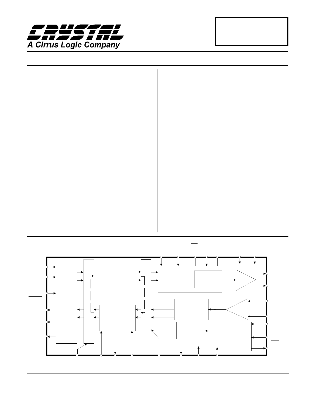
T1/E1 Line Interface
CS61574A
CS61575
Features
Provides Analog Transmission Line
•
Interface for T1 and E1 Applications
Provides Line Driver, Jitter Attenuator
•
and Clock Recovery Functions
Fully Compliant with AT&T 62411
•
Stratum 4 Jitter Requirements
Low Power Consumption
•
(typically 175 mW)
B8ZS/HDB3/AMI Encoder/Decoder
•
14 dB of Transmitter Return Loss
•
General Description
The CS61574A and CS61575 combine the complete
analog transmit and receive line interface for T1 or E1
applications in a low power, 28-pin device operating
from a +5V supply. Both devices support processorbased or stand-alone operation and interface with
industry standard T1 and E1 framers.
The receiver uses a digital Delay-Locked-Loop which is
continuously calibrated from a crystal reference to provide excellent stability and jitter tolerance. The
CS61574A has a receiver jitter attenuator optimized for
minimum delay in switching and transmission applications, while the CS61575 attenuator is optimized for
CPE applications subject to AT&T 62411 requirements.
The transmitter features internal pulse shaping and a
matched, constant impedance output stage to insure
signal quality on mismatched, poorly terminated lines.
Applications
• Interfacing Network Equipment such as DACS and
Channel Banks to a DSX-1 Cross Connect
• Interfacing Customer Premises Equipment to a
CSU
• Building Channel Service Units
TCLK
TPOS
[TDATA]
TNEG
[TCODE]
RCLK
RPOS
[RDATA]
RNEG
[BPV]
( ) = Pin Function in
[ ] = Pin Function in
2
3
4
AMI,
B8ZS,
HDB3,
8
CODER
7
6
RLOOP
(CS)
Host Mode
Extended Hardware Mode
R
E
M
O
T
E
L
O
O
P
B
A
C
K
26
XTALIN
JITTER
ATTENUATOR
9
XTALOUT10ACLKI
Crystal Semiconductor Corporation
P. O. Box 17847, Austin, Texas, 78760
(512) 445-7222 FAX:(512) 445-7581
ORDERING INFORMATION - See page 26.
MODE
L
O
C
A
L
L
O
O
P
B
A
C
K
1
LLOOP
(SCLK)
Copyright Crystal Semiconductor Corporation 1996
(CLKE)
TAOS
5
CONTROL
27
(All Rights Reserved)
(INT)
LEN0
28 23
CLOCK &
DATA
RECOVERY
SIGNAL
QUALITY
MONITOR
12 21
LOS
(SDI)
(SDO)
LEN1
LEN2
PULSE
SHAPER
LINE RECEIVER
RV+22RGND
TGND
2524
LINE DRIVER
DRIVER
MONITOR
14
TV+
15
13
16
19
20
17
18
11
TTIP
TRING
RTIP
RRING
MTIP
[RCODE]
MRING
[PCS]
DPM
[AIS]
MAY ’96
DS154F2
1
CS61574A CS61575
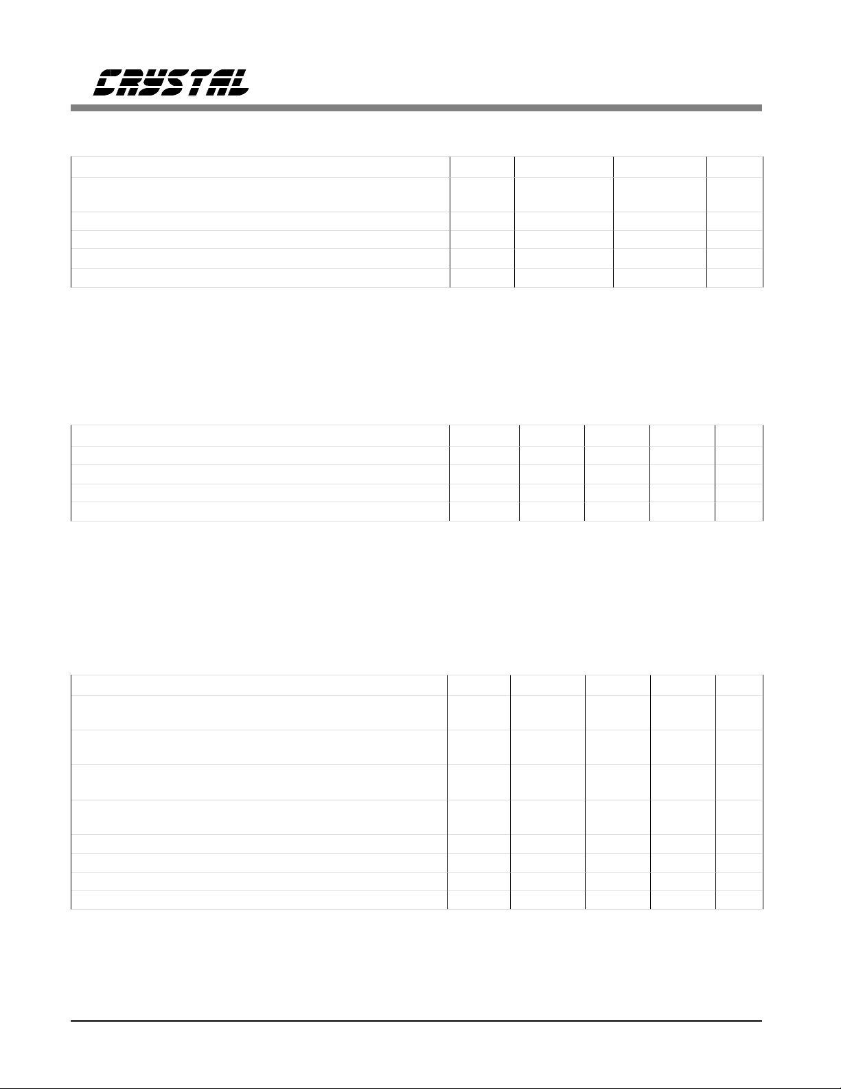
ABSOLUTE MAXIMUM RATINGS
Parameter Symbol Min Max Units
DC Supply (referenced to RGND, TGND=0V ) RV+
TV+
Input Voltage, Any Pin (Note 1) V
Input Current, Any Pin (Note 2) I
Ambient Operating Temperature T
Storage Temperature T
in
in
A
stg
-
-
6.0
(RV+) + 0.3
RGND-0.3 (RV+) + 0.3 V
-10 10 mA
-40 85
-65 150
WARNIN G: O perat ions at or beyond these l imits may resul t in perma nent da mage to t he devi ce.
Normal operation is not guaranteed at these extremes.
Notes: 1. Excluding RTIP, RRING, whic h must stay wit hin -6V to (RV+ ) + 0.3V.
2. Transient currents of up to 1 00 mA will not cause SCR la tch-up. Also TTIP, TRING, TV+ and TGND
can withstand a continuous current of 100 mA.
RECOMMENDED OPERATING CONDITIONS
Parameter Symbol Min Typ Max Units
DC Supply (Note 3) RV+, TV+ 4.75 5.0 5.25 V
Ambient Operating Temperature T
Power Consumption (Notes 4,5) P
Power Consumption (Notes 4,6) P
Notes: 3. TV+ must not exceed RV+ by more than 0.3V.
4. Power consumption while driving line load over operating temperature range. Includes IC and load.
Digital input levels are within 10% of the supply rails and digital outputs are driving a 50 pF
capacitive load.
5. Assumes 100% ones density and maximum line length at 5.25V.
6. Assumes 50% ones density and 300ft. line length at 5.0V.
A
C
C
-40 25 85
-290350mW
-175-mW
V
V
°C
°C
°C
DIGITAL CHARACTERISTICS (TA = -4 0°C to 85°C; T V+, RV+ = 5.0V ± 5%; GND = 0V)
Parameter Symbol Min Typ Ma x Units
High-Level Input Voltage (Notes 7, 8)
V
IH
PINS 1-4 , 17, 18 , 23-28
Low-Level Input Voltage (Notes 7, 8)
V
IL
PINS 1-4 , 17, 18 , 23-28
High-Level Output Voltage (Notes 7, 8, 9)
I
= -40 µA PINS 6-8, 11, 12, 25
OUT
Low-Level Output Voltage (Notes 7, 8, 9)
I
= 1.6 mA PINS 6-8, 11, 12, 23, 25
OUT
V
OH
V
OL
Input Leakage Current (Except Pin 5) - Low-Level Input Voltage, PIN 5 V
High-Level Input Voltage, PIN 5 V
Mid-Level Input Voltage, PIN 5 (Note 10) V
IL
IH
IM
Notes: 7. In Extended Hardware Mode, pins 17 and 18 are digital inputs. In Host Mode, pin 23 is
an open drain output and pin 25 is a tristate output.
8. This specification guarantees TTL compatibility (V
= 2.4V @ I
OH
9. Output drivers will drive CMOS logic levels into a CMOS load.
10. As a n a lter nat ive t o suppl yin g a 2.3- to -2.7 V in put, th is pin may b e le ft flo ati ng.
2 DS154F2
2.0 - - V
--0.8V
4.0 - - V
--0.4V
±10 µA
--0.2V
(RV+) - 0.2 - - V
2.3 - 2.7 V
= -40µA).
OUT
CS61574A CS61575
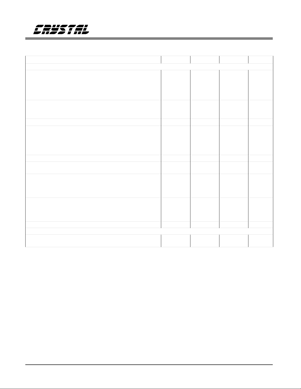
ANALOG SPECIFICATIONS (TA = -40°C to 85°C; TV+, RV+ = 5. 0V ±5%; GND = 0V)
Parameter Min Typ Max Units
Transmitter
AMI Output Pulse Amplitudes (Note 11)
E1, 75 Ω (Note 12)
E1, 120 Ω (Note 13)
T1, FCC Part 68 (Note 14)
T1, DSX-1 (Note 15)
E1 Zero (space ) level (LE N2/1/0 = 0 /0/0)
1:1 transformer and 75Ω load
1:1.26 transformer and 120Ω load
Recommended Output Load at TTIP and TRING - 75 Jitter Added During Remote Loopback (Note 16)
10Hz - 8kHz
8kHz - 40k Hz
10Hz - 40k Hz
Broad Band
Power in 2kHz band about 772kHz (Notes 11, 17) 12.6 15 17.9 dBm
Power in 2kHz band about 1.544MHz (Notes 11, 17)
(referenced to power in 2kHz band at 772kHz)
Positive to Negative Pulse Imbalance (Notes 11, 17)
T1, DSX-1
E1 amplitude at center of pulse
E1 pulse width at 50% of nominal amplitude
Transmitter Return Loss (Notes 11, 17, 18)
51 kHz to 102 kHz
102 kHz to 2.048 MHz
2.048 MHz to 3.072 MHz
Transmitter Short Circuit Current (Notes 11, 19) - - 50 mA RMS
2.14
2.7
2.7
2.4
-0.237
-0.3
-
-
-
-
-29 -3 8 - dB
-
-5
-5
8
14
10
Driver Performance Monitor
MTIP/MRING Sensitivity:
Differential Voltage Required for Detection - 0.6 - V
Notes: 11. Usi ng a 0.47 µF capacitor in series with the primary of a transformer recommended
in the Applications section.
12. Pulse amplitude measured at the output of a 1:1 or 1:1.26 transformer across a 75 Ω load for
line length setting LEN2/1/0 = 0/0/0.
13. Puls e ampli tude m easur ed at the ou tpu t of a 1:1. 26 tra nsfor mer acr oss a 12 0 Ω load for line length
setting LEN2/1/0 = 0/0/0.
14. Puls e ampli tude m easur ed at the ou tpu t of a 1:1. 15 tra nsfor mer acr oss a 10 0 Ω load for
line length setting LEN2/1/0 = 0/1/0.
15. Pulse amplitude measured at the DSX-1 cross-connect across a 100 Ω load for line length settings
LEN2/1/0 = 0/1/1, 1/0/0, 1/0/1, 1/1/0, or 1/1/1 using a 1:1.15 transformer and the length of #22 AWG,
ABAM, or equivalent cable specified in Table 3.
16. Input signal to RTIP/RRING is jitter free. Values will reduce slightly if jitter free clock is input to TCLK.
17. Not production tested. Parameters guaranteed by design and characterization.
18. Return loss = 20 log
= imped anc e of lin e loa d. Mea sur ed wi th a re pea ting 101 0 da ta p att ern wit h LEN 2/1 /0 = 0/ 0/0
z
0
and a 1:1 transformer terminated with a 75Ω load, or a 1:1.26 transformer terminated with a
120Ω load.
19. Measured broadband through a 0.5 Ω resistor across the secondary of a 1:1.26 transformer
during the transmission of an all ones data pattern for LEN2/1/0 = 0/0/0.
ABS((z1 +z0)/(z1-z0)) wher e z1 = impedance of the transmitter, and
10
2.37
3.0
3.0
3.0
-
-
0.005
0.008
0.010
0.015
0.2
-
-
-
-
-
2.6
3.3
3.3
3.6
0.237
0.3
0.02
0.025
0.025
0.05
0.5
5
5
-
-
-
V
V
V
V
V
V
Ω
UI
UI
UI
UI
dB
%
%
dB
dB
dB
DS154F2 3

CS61574A CS61575
ANALOG SPECIFICATIONS (TA = -40°C to 85°C; TV+, RV+ = 5. 0V ±5%; GND = 0V)
Parameter Min Typ Max Units
Receiver
RTIP/RRING Input Impedance - 50k Sensitivity Below DSX (0dB = 2.4V) -13.6
500
Data Decision Threshold
T1, DSX-1 (Note 20)
T1, DSX-1 (Note 21)
T1, FCC Part 68 and E1 (Note 22)
60
53
45
Allowable Consecutive Zeros before LOS 160 175 190 bits
Receiver Input Jitter Tolerance (Note 23)
10kHz - 100kHz
2kHz
10Hz and below
0.4
6.0
300
Loss of Signal Threshold (Note 24) 0.25 0.30 0.50 V
Notes: 20. For input amplitude of 1.2 V
21. For input amplitude of 0.5 V
22. For input amplitude of 1.05 V
to 4. 14 Vpk.
pk
to 1.2 Vpk and from 4. 14 Vpk to RV+.
pk
to 3.3 Vpk.
pk
23. Jitter tolerance increases at lower frequencies. See Figure 11.
24. The analog input squelch circuit shall operate when the input signal amplitude above ground on the
RTIP and RRING pins falls within the range of 0.25V to 0.50V. Operation of the squelch results in
the recovery of zeros. During receive LOS, the RPOS, RNEG or RDATA outputs are forced low.
65
65
50
-
-
-
-
-
70
77
55
-
-
dB
mV
% of peak
% of peak
% of peak
-
-
-
UI
UI
UI
Ω
4 DS154F2

CS61574A CS61575
ANALOG SPECIFICATIONS (TA = -40°C to 85°C; TV+, RV+ = 5. 0V ±5%; GND = 0V)
Parameter Min Typ Max Units
Jitter Attenuator
Jitter Attenuation Curve Corner Frequency (Notes 17, 25)
CS61574A
CS61575
CS61574A T1 Receiver Jitter Transfer (Notes 25, 26)
Jitter Freq. [Hz] Amplitude [UIpp]
10 10
100 10
500 10
1k 5
10k, 40k 0.3
CS61575 T1 Receiver Jitter Transfer (Notes 25, 26)
Jitter Freq. [Hz] Amplitude [UIpp]
10 10
100 10
500 10
1k 5
10k, 40k 0.3
CS61574A E1 Receiver Jitter Transfer (Notes 26, 27, 28)
Jitter Freq. [Hz] Amplitude [UIpp]
10 1.5
20 1.5
100 1.5
400 1.5
1k 1.5
10k, 100k 0.2
CS61575 E1 Receiver Jitter Transfer (Notes 26, 27, 28)
Jitter Freq. [Hz] Amplitude [UIpp]
10 1.5
20 1.5
100 1.5
400 1.5
1k 1.5
10k, 100k 0.2
Attenuator Input Jitter Tolerance (Notes 17, 28)
(Bef ore Onse t of FI FO Overf low or Underf low Pro tect ion)
CS61574A
CS61575
Notes: 25. Attenuation measured at the demodulator output of an HP3785B with input jitter equal to 3/4 of
measured jitter tolerance using a measurement bandwidth of 1 Hz (10<f<100Hz), 4Hz (100<f<1000
Hz) and 10 Hz (f> 1kHz) centered around the jitter frequency. With a 2
26. Crystal must meet specifications described in CXT6176/CXT8192 data sheet.
27. Jitter measured at the demodulator output of an HP3785A (or equivalent) using a measurement
bandwidth not to exceed 20 Hz centered around the jitter frequency. With a 2
28. Jitter below 100 kHz and within the attenuator’s input jitter tolerance is not translated or aliased to
other frequencies. Output jitter increases significantly when attenuator input jitter tolerance is
exceeded.
-
-
3.0
20
35
40
40
6.0
23
38
40
40
3.0
6.0
20
30
35
35
6.0
12
22
30
35
35
12
138
6
3
6.0
30
40
50
50
9.0
33
43
50
50
6.0
12
32
40
45
45
12
18
29
39
45
45
23
-
15
-1 PRBS data pattern.
-
-
-
-
-
-
-
-
-
-
-
-
-
-
-
-
-
-
-
-
-
-
-
-
-
-
15
-1 PRBS data pattern.
Hz
Hz
dB
dB
dB
dB
dB
dB
dB
dB
dB
dB
dB
dB
dB
dB
dB
dB
dB
dB
dB
dB
dB
dB
UI
UI
DS154F2 5

CS61574A CS61575
T1 SWITCHING CHARACTERISTICS (TA = -40°C to 85°C; TV+, RV+ = 5.0V ±5%;
GND = 0V; Inputs: Logic 0 = 0V, Logic 1 = RV+; See Figures 1, 2, & 3)
Parameter Symbol Min Typ Max Units
Crystal Frequency (Note 26) f
TCLK Frequency f
TCLK Pulse Width (Note 29) t
ACLKI Duty Cycle t
ACLKI Frequency (Note 30) f
RCLK Duty Cycle (Note 31) t
Rise Time, All Digital Outputs (Note 32) t
Fall Time, All Digital Outputs (Note 32) t
TPOS/TNEG (TDATA) to TCLK Falling Setup Time t
TCLK Falling to TPOS/TNEG (TDATA) Hold Time t
RPOS/RNEG Valid Before RCLK Falling (Note 33) t
RDATA Valid Before RCLK Falling (Note 3 4) t
RPOS/RNEG Valid Before RCLK Rising (Note 35) t
RPOS/RNEG Valid After RCLK Falling (Note 33) t
RDATA Valid After RCLK Falling (Note 34) t
RPOS/RNEG Valid After RCLK Rising (Note 35) t
c
tclk
pwh2
pwh3/tpw3
aclki
pwh1/tpw1
r
f
su2
h2
su1
su1
su1
h1
h1
h1
Notes: 29. The transmitted pulse width does not depend on the TCLK duty cycle.
30. ACLKI provided by an external source or TCLK.
31. RCLK duty cycle will be 62.5% o r 37.5% when jitte r attenuator limit s are reach ed.
32. At max load of 1.6 mA and 50 pF.
33. Host Mode (CLKE = 1).
34. Extended Hardware Mode.
35. Hardware Mode, or Host Mode (CLKE = 0).
- 6.176000 - MHz
-1.544-MHz
150 - 500 ns
40 - 60 %
-1.544-MHz
45 50 55 %
- - 85 ns
- - 85 ns
25 - - ns
25 - - ns
150 274 - ns
150 274 - ns
150 274 - ns
150 274 - ns
150 274 - ns
150 274 - ns
E1 SWITCHING CHARACTERISTICS (TA = -4 0°C to 85 °C; TV+, RV+ = 5.0V ±5%;
GND = 0V; Inputs: Logic 0 = 0V, Logic 1 = RV+; See Figures 1, 2, & 3)
Parameter Symbol Min Typ Max Units
Crystal Frequency (Note 26) f
TCLK Frequency f
TCLK Pulse Width (Note 29) t
ACLKI Duty Cycle t
ACLKI Frequency (Note 30) f
RCLK Duty Cycle (Note 31) t
Rise Time, All Digital Outputs (Note 32) t
Fall Time, All Digital Outputs (Note 32) t
TPOS/TNEG (TDATA) to TCLK Falling Setup Time t
TCLK Falling to TPOS/TNEG (TDATA) Hold Time t
RPOS/RNEG Valid Before RCLK Falling (Note 33) t
RDATA Valid Before RCLK Falling (Note 3 4) t
RPOS/RNEG Valid Before RCLK Rising (Note 35) t
RPOS/RNEG Valid After RCLK Falling (Note 33) t
RDATA Valid After RCLK Falling (Note 34) t
RPOS/RNEG Valid After RCLK Rising (Note 35) t
c
tclk
pwh2
pwh3/tpw3
aclki
pwh1/tpw1
r
f
su2
h2
su1
su1
su1
h1
h1
h1
6 DS154F2
- 8.192000 - MHz
-2.048-MHz
150 - 340 ns
40 - 60 %
-2.048-MHz
45 50 55 %
- - 85 ns
- - 85 ns
25 - - ns
25 - - ns
100 194 - ns
100 194 - ns
100 194 - ns
100 194 - ns
100 194 - ns
100 194 - ns
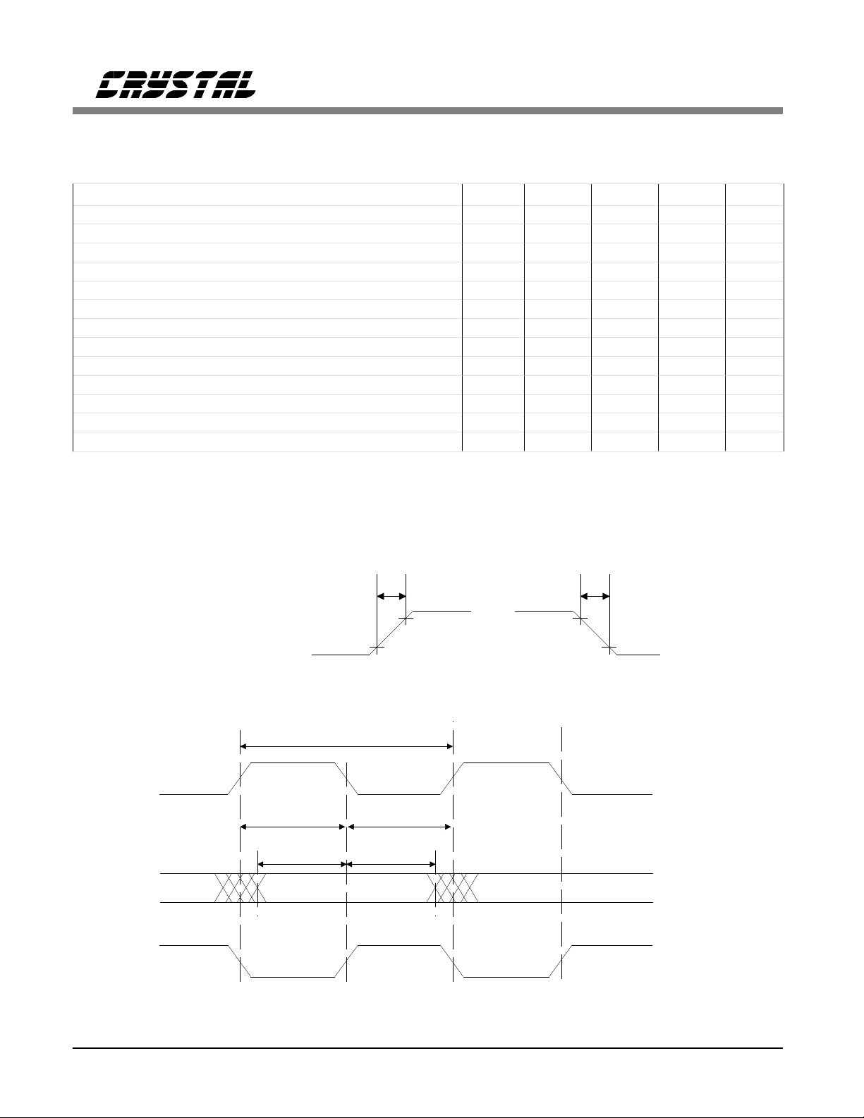
SWITCHING CHARACTERISTICS (TA = -40 ° to 85°C; TV +, RV+ = ±5% ;
Inputs: Logic 0 = 0V, Logic 1 = RV+)
Parameter Symbol Min Typ Max Units
SDI to SCLK Setup Time t
SCLK to SDI Hold Time t
SCLK Low Time t
SCLK High Time t
SCLK Rise and Fall Time t
CS to SCLK Setup Time t
SCLK to CS Hold Time t
CS Inactive Time t
SCLK to SDO Valid (Note 36) t
CS to SDO High Z t
Input Valid To PCS Falling Setup Time t
PCS Rising to Input Invalid Hold Time t
PCS Active Low Time t
Notes: 36. Output load capacitance = 50pF.
dc
cdh
cl
ch
, t
r
cc
cch
cwh
cdv
cdz
su4
h4
pcsl
f
50 - - ns
50 - - ns
240 - - ns
240 - - ns
- - 50 ns
50 - - ns
50 - - ns
250 - - ns
- - 200 ns
- 100 - ns
50 - - ns
50 - - ns
250 - - ns
CS61574A CS61575
RCLK
RPOS
RNEG
RDATA
BPV
RCLK
Any Digital Output
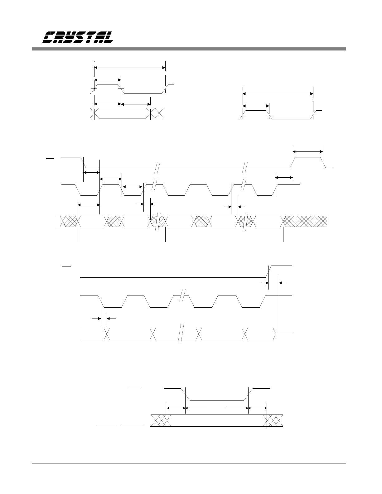
Figure 1. Signal Rise and Fall Characteristics
t
pwl1
tt
su1
t
pw1
t
r
90% 90%
10%
t
pwh1
h1
10%
t
f
EXTENDED
HARDWARE
MODE OR
HOST MODE
(CLKE = 1)
HARDWARE
MODE OR
HOST MODE
(CLKE = 0)
Figure 2. Recovered Clock and Data Switching Characteristics
DS154F2 7
TCLK
t
pwh2
t
su2
t
pw2
CS61574A CS61575
t
pw3
t
h2
t
pwh3
TPOS/TNEG
Figure 3a. Transmit Clock and Data Switching
Charact er ist ic s
CS
t
ch
CONTROL BYTE DATA BYTE
t
cl
t
cdh
Figure 4. Serial Port Write Timing Diagram
SCLK
SDI
t
cc
t
dc
LSB LSB
CS
ACLKI
Figure 3b. Alternate External Clock Characteristics
t
cwh
t
cch
t
cdh
MSB
t
cdz
SCLK
t
cdv
SDO
HIGH Z
CLKE = 1
Figure 5. Seria l Port R ead Timi ng Di agra m
PCS
t
h4
LEN0/1/2 , T A OS,
RLOOP, LLOOP,
t
su4
t
pcsl
VALID INPUT DATA
RCODE, TCODE
Figure 6. Exte nded Ha rdwa re Mo de Par allel Chip Select Timin g Dia gram
8 DS154F2

CS61574A CS61575
THEORY OF OPERATION
Enhancements in CS61575 and CS61574A
The CS61574A a nd CS61575 provid e high er p erformance and more features than the CS61574
including:
• AT&T 62411, Stratum 4 complian t jitter at-
tenuation over the full rang e of operatin g
frequency and jitte r amplitude (CS6157 5),
• 50% lower power consumption,
• Internally matched trans mitter outpu t im-
pedance for improved signal q uality,
• Optional AMI, B8ZS, HDB3 enc oder/de-
coder or external line coding support,
• Receiver AIS (unframed all ones ) detect ion,
• ANSI T1.231-1993 compliant receiver
LOS (Loss of Signal) handli ng,
• Transmitter TTIP and TRING ou tputs are
forced low when TCLK is static,
• The Driver Performan ce Monitor op erates
over a wider range of input signal levels.
Existing design s using the CS61574 can be converted to th e higher perform ance, pin-co mpatible
CS61574A or CS61575 if the transmit transformer is replaced by a pin-compatible
transformer with a new turns ratio.
Understanding the Difference Between the
CS61575 and CS61 574A
The CS61574A and CS61575 provide receiver
jitter attenuation performance optimized for different appli cations. The CS6 1575 is optimize d to
attenuate l arge amplitud e, low fre quency jitte r for
T1 Customer Prem ises Equi pm ent ( CPE ) app lications as required by AT&T 62411. The
CS61574A is optimized to minimize data delay in
T1 and E1 switching or transmission applications.
Refer to the "Jitter Attenuator" section for additional information.
Introduction to Operating Modes
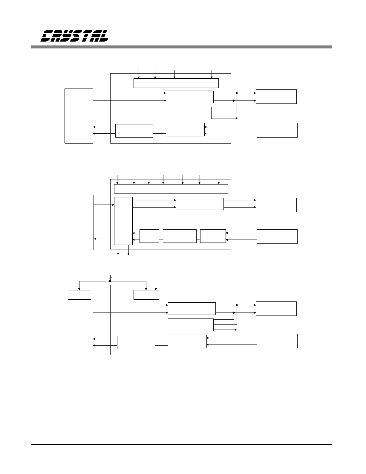
The CS61574A and CS61 575 support three operating modes wh ich are s electe d by th e level of the
MODE pin as shown in Tables 1 and 2, Figure 7,
and Figures A1-A3 of the Applications section.
The modes are Hardware Mode, E xtended Hardware Mode, and Host Mode. In Hardware and
Extended Hardware Modes, discre te pin s are used
to configure and monitor the device. The Extended Hardware Mode provides a parallel chip
select input which latches the control inputs allowing individual ICs to be configured using a
common set of control lines. In the Host Mode,
an external processor monito rs and configures the
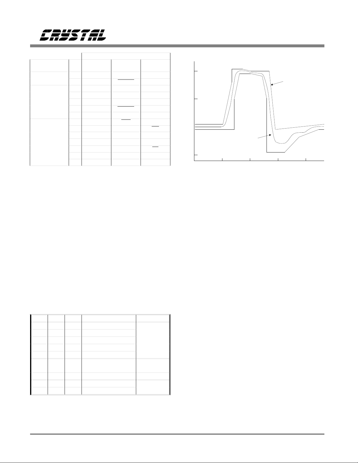
device through a serial interface. There are thirteen multi-function pins whose functionality is
determined by the operating mode. (see Table 2).
Hardware
Mode
Control
Method
MODE
Pin
Level
Line
Coding
AIS
Detection
Driver
Performance
Monitor
Table 1. Diff erences Betwe en Operati ng Modes
Control
Pins
<0.2 V Floating or
External Internal-
No Yes No
Yes No Yes
Extended
Hardware
Mode
Control Pins
with Parallel
Chip Select
2.5 V
AMI, B8ZS,
or HDB3
Host
Mode
Serial
Interface
>(R V+)-0.2
V
External
DS154F2 9
CS62180B
FRAMER
CIRCUIT
T1 or E1
REPEATER
OR
MUX
TNEG
RPOS
RNEG
TDATA
RDATA
CS61575
CS61574A
JITTER
ATTENUATOR
RCODETCODE
AMI
B8ZS,
HDB3,
CODER
HARDWARE MODE
RLOOP LEN0/1/2LLOOPTAOS
CONTROL
LINE DRIVER
DRIVER MONITOR
LINE RECEIVER
EXTENDED HARDWARE MODE
RLOOP PCS LEN0/1/2LLOOPTAOS
CONTROL
LINE DRIVER
CS61575
CS61574A
AIS
DETECT
JITTER
ATTENUATOR
MRING
MTIP
LINE
RECEIVER
TTIPTPOS
TRING
DPM
RTIP
RRING
TTIP
TRING
RTIP
RRING
CS61574A CS61575
TRANSMIT
TRANSFORMER
RECEIVE
TRANSFORMER
TRANSMIT
TRANSFORMER
RECEIVE
TRANSFORMER
CONTROL
CS62180B
FRAMER
CIRCUIT
BPV AIS
P SERIAL PORT
µ
5
TPOS
TNEG
RPOS
RNEG
HOST MODE
CLKE
CONTROL
LINE DRIVER
CS61575
CS61574A
JITTER
ATTENUATOR
DRIVER MONITOR
LINE RECEIVER
Figure 7. Overv iew of Op eratin g Mode s
MRING
MTIP
TTIP
TRING
DPM
RTIP
RRING
TRANSMIT
TRANSFORMER
RECEIVE
TRANSFORMER
10 DS154F2
CS61574A CS61575
MODE
FUNCTION PIN HARDWARE
TRANSMITTER
RECEIVER/ DPM
CONTROL
3TPOS TDATA TPOS
4TNEG
6 RNE G BPV RNEG
7RPOS RDATA RPOS
11 DPM AIS DPM
17 MTIP
18 MRI NG - MRING
18 23 LEN0 LEN0
24 LEN1 LEN1 SDI
25 LEN2 LEN2 SDO
26 RLOOP RLOOP
27 LLOOP LLOOP SCLK
28 TAOS TAOS CLKE
EXTENDED
HARDWARE
TCODE TNEG
RCODE MTIP
PCS -
HOST
INT
CS
Table 2. Pin Definitions
Transmitter
The transmitter takes digita l T1 or E1 input data
and drives appropriately shaped bipolar pulses
onto a transmission line. The transmit data (TPOS
& TNEG or TDATA) is supplied synchronously
and sampled on the falling edge of the input
clock, TCLK.
Either T1 (DSX-1 or Network Interface) or E1
CCITT G.703 pulse shapes may be selected.
Pulse shaping and signal level are controlled by
"line length select" inputs as shown in Table 3.
LEN2 LEN1 LEN0 Option Selected Application
0 1 1 0-133 FEET
1 0 0 133-266 FEET
1 0 1 266-399 FEET
1 1 0 399-533 FEET
1 1 1 533-655 FEET
000
0 0 1 AT&T CB113 Repeater
0 1 0 FCC PART 68, OPT. A Network
011 ANSI T1.403
120Ω (1:1.26)
75Ω (1:1)
Table 3. Line Length Selection
DSX-1
ABAM
(AT&T 600B
or 600C)
E1
CCITT G.703
Interface
NORMALIZED
AMPLITUDE
1.0
0.5
0
OUTPUT
PULSE SHAPE
-0.5
0 250 750 1000
500
TIME (nanoseconds)
ANSI TI.102,
AT&T CB 119
SPECIFICATIONS
Figure 8. Typical Pulse Shape at DSX-1 Cross Connect
The CS61575 and CS6157 4A line drivers are designed to drive a 75 Ω equivalent load.
For E1 applicatio ns, t he C S615 74A a nd CS615 75
drivers provide 14 dB of return loss during the
transm ission o f both mark s and sp aces. This i mproves signal quality by minimizing reflections
off the transmitter. Similar levels of return loss
are provided for T1 applications.
For T1 DSX-1 applications, line len gths from 0 to
655 feet (as measured from the transmitter to the
DSX-1 cross connect ) may be selected. The five
partition arrangement in Table 3 meets ANSI
T1.102 and AT&T CB-119 requirements when
using #22 ABAM cable. A ty pical outp ut puls e is
shown in Figu re 8. These pulse s ettings can also
be used to meet CCITT puls e shape requi rements
for 1.544 MHz operation.
For T1 Network Interface applications , two additional opt ions are pr ovided. Note t hat the opt imal
pulse width for Part 68 (32 4 ns) is narrower than
the optimal puls e width for DSX-1 (350 ns). T he
CS61575 and CS61574A automatically adjusts
the pulse width based upon the "lin e length" selection made.
DS154F2 11
CS61574A CS61575
Percent of
nominal
peak
voltage
120
110
100
90
80
50
10
0
-10
-20
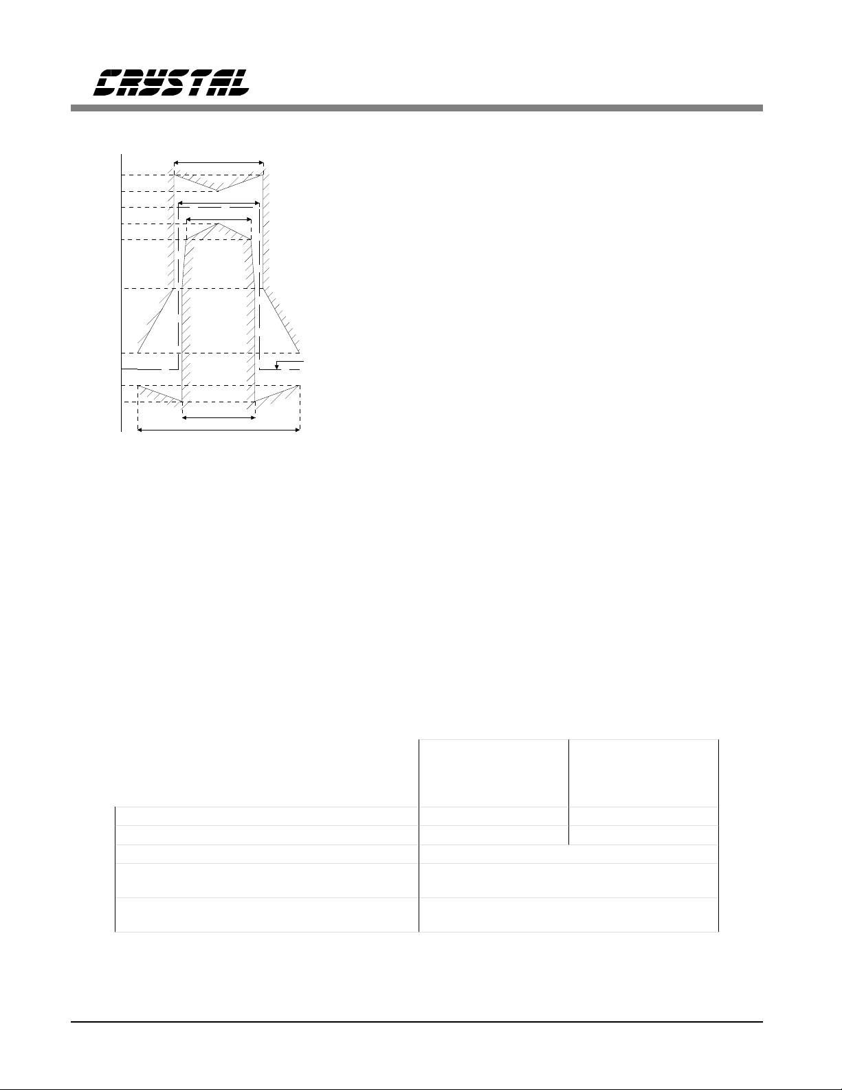
Figure 9. Mask of the Pulse at the 2048 kbps Interface
269 ns
244 ns
194 ns
Nominal Pulse
219 ns
488 ns
The E1 G.703 pu lse shape is supported wit h line
length selection LEN2/1/0=0/0/0. The pulse
width will meet the G.703 pulse shape template
shown in Figure 9, and specified in Table 4.
The CS61574A an d CS61575 will detect a static
TCLK, and will force TTIP and TRING low to
prevent transmission when data is not present.
When any transmit control pin (TAOS, LEN0-2
or LLOOP) is toggled, the transmitter outputs
will require appro ximat ely 22 bi t pe riod s to stab ilize. The transmitter will take longer to stabilize
when RLOOP is select ed because the timing circuitry must adjust to the new frequency.
Transmit All On es Select
The transmitte r provides for all ones insertion at
the frequency of TCLK. Transmit all ones is selected when TAOS goes high, and causes
continuous ones to be transmitted on the line
(TTIP and TRING). In this mode, the TPOS and
TNEG (or TDATA) inputs are ignored. If Remote
Loopback i s in effect, any TAOS request will be
ignored.
Receiver
The receiver extracts dat a an d cl ock fro m an AMI
(Alternate Mark Inversion) coded signal and outputs clock an d synchronized data. The receiver is
sensitive to signals over the entire range of
ABAM cable lengths and requires no equalizati on
or ALBO (Automatic Line Build Out) circuits.
The signal is received on both ends of a centertapped, center-grounded transformer. The
transformer is center tapped on the IC side. The
clock and dat a recovery circuit exceeds the jitter
tolerance specifications of Publications 43802,
43801, AT&T 62411, TR-TSY-000170, and
CCITT REC. G.823.
For coaxial cable,
75Ω load and
transformer specified
in Application Section.
Nominal peak voltage of a mark (puls e) 2.37 V 3 V
Pea k voltage of a space (no pulse)
Nominal puls e wi dt h 244 ns
Ratio of the amplitudes of positive and negative
pulses at the center of the pulse interval
Ratio of the widths of positive and negative
pulses at the nomi nal half amplitude
* When configured with a 0.47 µF nonpolarized capacitor in series with the TX transformer
primary as shown in Figures A1, A2 and A3.
Table 4. CCITT G.703 S pecificati ons
12 DS154F2
0 ±0.237 V 0 ±0.30 V
0.95 to 1.05*
0.95 to 1.05*
For shielded twisted
pair, 120Ω load and
transformer specified
in Application Section.
CS61574A CS61575
RTIP
1 : 2
RRING
Data
Level
Slicer
Edge
Detector
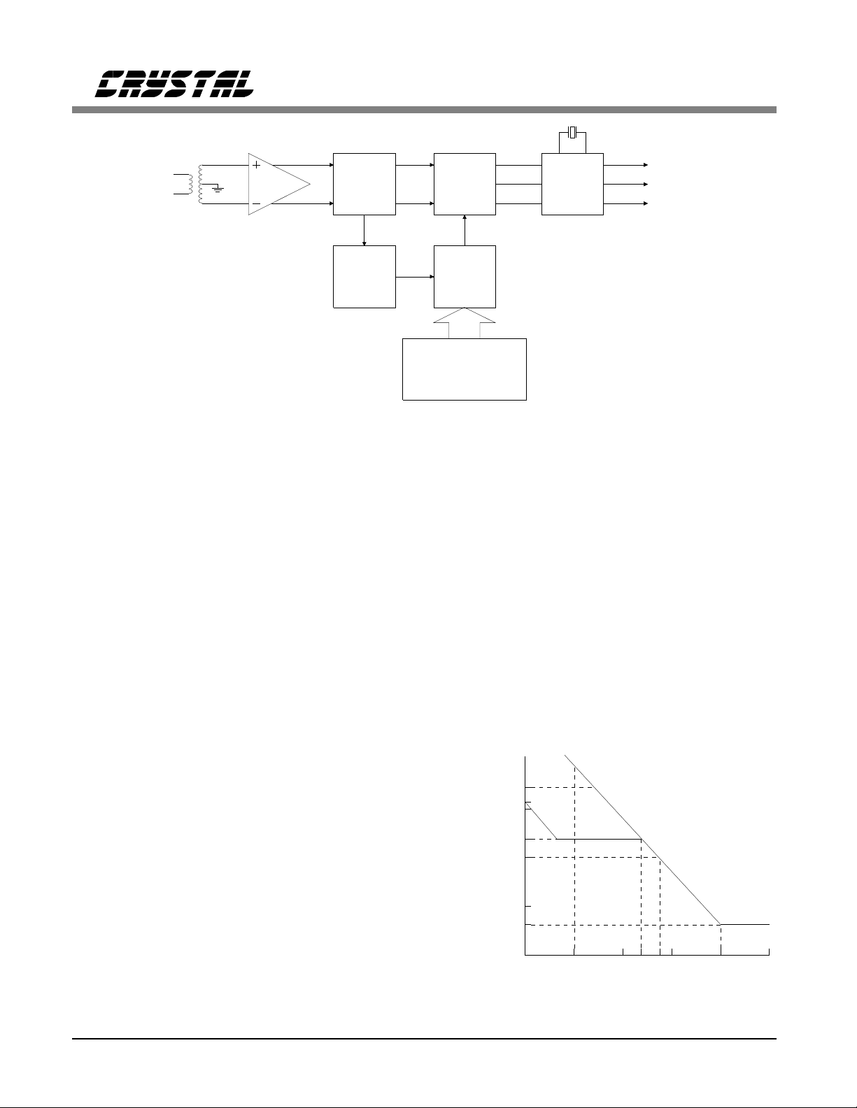
Figure 1 0. Re cei ver Bl oc k Di agr am
A block diagram of the rece iver is shown in Figure 10. The two leads of the transformer (RTIP
and RRING) have opp osite polarity allowing th e
receiver to treat RTIP and RRING as unipolar signals. Comparators are used to detect pulses on
RTIP and RR ING. The compar ator thre shold s are
dynamically established at a percent of the peak
level (50% of peak for E1, 65% of peak for T1;
with the slicing level selected by LEN2/1/0 inputs).
The leading edge of an incoming data pulse triggers the clock ph ase selector. The phase selector
chooses one of t he 13 available phases which th e
delay line pro duces for each bit perio d. The output from the phase selector feeds the clock and
data recovery circuits which generate the recovered clock and sample the incoming signal at
appropriate intervals to recover the data.
Data sampling will continue at the periods selected by the phase selector until an incoming
pulse deviates enou gh to cause a new phase to be
selected for da ta sampling. The phases of the d elay line are selected and updated to allow as much
as 0.4 UI of jitter from 10 kHz to 100 kHz, without error. The jitter tolerance of the receiver
exceeds that shown in Figure 11. Additionally,
this method o f clock and d ata recovery is tol erant
of long strings of consecutive zeros. The data
Data
Sampling
& Clock
Extraction
Clock
Phase
Selector
Continuously
Calibrated
Delay Line
Jitter
Attenuator
RPOS
RNEG
RCLK
sampler will continuously sample data based on
its last input until a new pulse arrives to update
the clock phase selector.
The delay line is continuously calibrated using
the crystal oscillator reference clock. The delay
line produces 13 phases for eac h cycle of the reference clock. In effect, the 13 phases are
analogous to a 20 MHz clock when the reference
clock is 1.544 MHz. This implementation utilizes
the benefits of a 2 0 MHz clo ck for cl ock recovery
without actually having the clock present to impede analog circuit performance.
Minimum
300
138
PEAK-TO-PEAK
JITTER
(unit intervals)
100
28
10
1
.4
.1
AT&T 62 411
Figure 11. Minimum Inpu t Jitter Tole rance of R eceiver
Performance
10
JITT E R F R E QUENC Y (Hz)
300
1k
10k1 100 100k700
DS154F2 13
CS61574A CS61575
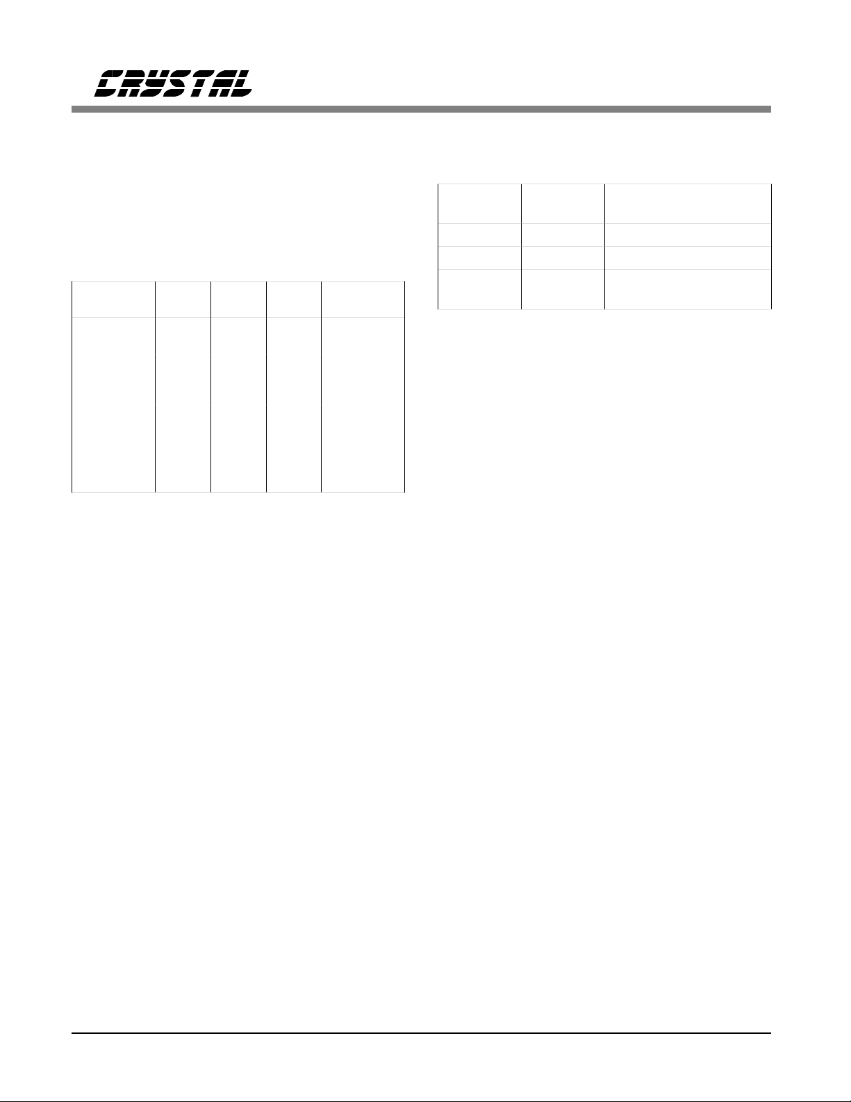
In the Hardware Mode, da ta at RPOS and RNEG
should be sampled on the rising edge of RCLK,
the recovered clock. In the Extended Hardware
Mode, data at RDATA should be sampled on th e
falling edge o f RCLK. In the Host Mode , CLKE
determines the clock polarity for which output
data should be sampled as shown in Table 5.
MODE
(pin 5)
LOW
(<0.2V)
HIGH
(>(V+) - 0.2V)
HIGH
(>(V+) - 0.2V)
MIDDLE
(2.5V)
X = Don’t care
Table 5. Data Ou tput/Clock Relatio nship
CLKE
(pin 28)
XRPOS
LOW RPOS
HIGH RPOS
X RDATA RCLK Falling
DATA CLOCK Clock Edge
for V alid Data
RCLK
RNEG
RNEG
SDO
RNEG
SDO
RCLK
RCLK
RCLK
SCLK
RCLK
RCLK
SCLK
Rising
Rising
Rising
Rising
Falling
Falling
Falling
Rising
Loss of Signal
The receiver will indicate loss of signal after
power-up, reset or upon receiving 175 consecutive zeros. A digital counter counts received
zeros, base d on RCLK cycles. A zero is received
when the RTIP and RRING inputs are below the
input comparator slicing threshold level established by the peak detector. After the signal is
removed for a period of time the data slicing
threshold level decays to approximately
300 mV
peak
.
If ACLKI is present during the LOS state, ACLKI
is switched int o the input of the jitter attenua tor,
resulting in RCLK matching the frequency of
ACLKI. The jitter attenuator buffers any inst antaneous changes in phase between the last
recovered clock and the ACLKI reference clock.
This means that RCLK will smoothly transition
to the new frequency. If ACLKI is not present,
then the crys tal os cil lator of t he j itter atten uat or is
forced t o its center frequ ency. Ta ble 6 shows the
status of RCLK upon LOS.
Crystal
present?
No Yes ACLKI
Yes No Centered Crystal
Yes Yes
ACLKI
present?
Table 6. RC LK Stat us at L OS
Source of RCLK
ACLKI via the
Jitter Attenuator
Jitter Attenuator
The jitter at tenuator reduces wander and jitte r in
the recovered clock si gnal. It consists of a 32 or
192-bit FIFO, a crystal oscillator, a set of load
capacitors for the crystal, and control logic. The
jitter attenuator exceeds the jitter attenuation requirements of Publications 43802 and REC.
G.742. A typi cal jitter a ttenuation cu rve is shown
in Figure 12. The CS61575 fully meets AT&T
62411 jitter attenuation requirements. The
CS61574A will have a discontinuity in the jitter
transfer function whe n the incoming jitter amplitude exceeds approximately 23 UIs.
The jitter attenu ator works in the following manner. The recovered clock and data are in put to t he
FIFO with the recovered clock controlling the
FIFO’s write pointer. The crystal oscillator controls the FIFO’s read pointer which reads data out
of the FIFO and presents it at RPOS and RNEG
(or RDATA). RCLK is equivalent to the oscillator’s output. By changing the load capacitance
that the IC presents to the crystal, the oscillatior
frequency (and RCLK) is a djusted to the average
frequency of the recovered signal. Logic determines the phase relationship between the read and
write pointe rs and decid es how to adjust the lo ad
capacitance o f th e c rystal . Jitte r is ab so rbed in the
FIFO accordi ng to t he jitt er tra nsfer ch aracteri stic
shown in Figure 12.
14 DS154F2
 Loading...