

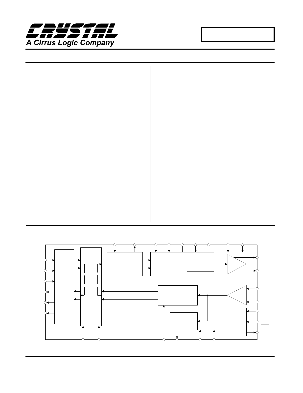
T1/E1 Line Interface
CS61535A
Features
Provides Analog PCM Line Interface
•
for T1 and E1 Applications
Provides Line Driver, and Data and
•
Clock Recovery Functions
Transmit Side Jitter Attenuation
•
Starting at 6 Hz, with > 300 UI of Jitter
Tolerance
Low Power Consumption
•
(typically 175 mW)
B8ZS/HDB3/AMI Encoders/Decoders
•
14 dB of Transmitter Return Loss
•
Compatible with SONET, M13 , CCITT
•
G.742, and Other Asynchronous
Muxes
General Description
The CS61535A combines the complete analog transmit
and receive line interface for T1 or E1 applications in a
low power, 28-pi n dev i ce operating from a +5V su ppl y .
The device features a transmitter jitter attenuator making it ideal for use in asynchro nous multiplexor s ystems
with gapped transmit clocks. The CS61535A provides a
matched, constant impedance output stage to insure
signal qualit y on m ism atched, poorly term inated lines.
Both ICs use a digital Delay-Locked-Loop clock and
data recovery circuit which is continuously calibrated
from a crystal reference to provide excellent stability
and jitter tolerance.
Applications
• Interfacing network transmission equipment such as
SONET multiplexor and M13 to a DSX-1 cross connect.
• Interfacing customer premis es equipment to a CSU.
• Interfacing to E1 links.
Ordering Information
CS61535A-IP1 28 Pin Plastic DIP
CS61535A-IL1 28 Pin PLCC (j-leads)
[ ] = Pin Function in
( ) = Pin Function in
TCLK
TPOS
[TDATA]
TNEG
[TCODE]
RCLK
RPOS
[RDATA]
RNEG
[BPV]
2
3
4
8
7
6
B8ZS,
HDB3
CODER
Extended Hardware Mode
Host Mode
AMI,
LOOP
BACK
26
(CS)
LLOOP
(SCLK)
RLOOP
27
Crystal Semiconductor Corporation
P.O. Box 17847, Austin, TX 78760
(512) 445-7222 FAX: (512) 445-7581
XTALIN
XTALOUT
9
JITTER
ATTENUATOR
(INT)
(SDI)
(CLKE)
MODE
10
Copyright Crystal Semiconductor Corporation 1996
5
CONTROL
ACLKI
LEN0
TAOS
28 23
CLOCK &
DATA
RECOVERY
SIGNAL
QUALITY
MONITOR
12 21
1
LOS
(All Rights Reserved)
(SDO)
LEN1
LEN2
PULSE
SHAPER
RV+22RGND
TGND
2524
LINE DRIVER
LINE RECEIVER
MONITOR
14
DRIVER
TV+
15
13
16
19
20
17
18
11
MAY ’96
TTIP
TRING
RTIP
RRING
MTIP
[RCODE]
MRING
[PCS]
DPM
[AIS]
DS40F2
1

CS61535A
ABSOLUTE MAXIMUM RATINGS
Parameter Symbol Min Max Units
DC Supply (referenced to RGND,TGND=0V) RV+
TV+
Input Voltage, Any Pin (Note 1) V
Input Current, Any Pin (Note 2) I
Ambient Operating Temperature T
Storage Temperature T
in
in
A
stg
-
-
6.0
(RV+) + 0.3
RGND-0.3 (RV+) + 0.3 V
-10 10 mA
-40 85
-65 150
WARNIN G: O perat ions at or beyond these l imits may resul t in perma nent da mage to t he devi ce.
Normal operation is not guaranteed at these extremes.
Notes: 1. Excluding RTIP, RRING, whic h must stay wit hin -6V to (RV+ ) + 0.3V.
2. Transient currents of up to 1 00 mA will not cause SCR la tch-up. Also TTIP, TRING, TV+ and TGND
can withstand a continuous current of 100 mA.
RECOMMENDED OPERATING CONDITIONS
Parameter Symbol Min Typ Max Units
DC Supply (Note 3) RV+, TV+ 4.75 5.0 5.25 V
Ambient Operating Temperature T
Power Consumption (Notes 4, 5) P
Power Consumption (Notes 4, 6) P
Notes: 3. TV+ must not exceed RV+ by more than 0.3V.
4. Power consumption while driving line load over operating temperature range. Includes IC and load.
Digital input levels are within 10% of the supply rails and digital outputs are driving a 50 pF load.
5. Assumes 100% ones density and maximum line length at 5.25V.
6. Assumes 50% ones density and 300ft. line length at 5.0V.
A
C
C
-40 25 85
-290350mW
-175-mW
V
V
°C
°C
°C
2 DS40F2
CS61535A
DIGITAL CHARACTERISTICS (TA = -40°C to 8 5°C; TV+, RV + = 5.0V ±5%; GND = 0V)
Parameter Symbol Min Typ Ma x Units
High-Level Input Voltage
Pins 1-4 , 17, 18 , 23-28 (No tes 7, 8, 9) V
IH
Low-Level Input Voltage
Pins 1-4 , 17, 18 , 23-28 (No tes 7, 8, 9) V
High-Level Output Voltage (I
Pins 6-8 , 11, 12 , 25 (Notes 7, 8, 10)
Low-Level Output Voltage (I
Pins 6-8 , 11, 12 , 23, 25 (Notes 7, 8, 10) V
OUT
OUT
= -40 µA)
= 1.6 mA)
IL
V
OH
OL
Input Leakage Current (Except Pin 5) - Low-Level Input Voltage, Pin 5 V
High-Level Input Voltage, Pin 5 V
Mid-Level Input Voltage, Pin 5 (Note 11) V
Notes: 7. This specification guarantees TTL compatibility (V
IL
IH
IM
= 2.4V @ I
OH
8. In Host Mode, pin 23 is an open drain output and pin 25 is a tristate output.
9. Pins 17 and 18 of the CS61535A are digital inputs in the Extended Hardware Mode.
10. Output drivers will drive CMOS logic levels int o a CMOS load.
11. As a n a lter nat ive t o suppl yin g a 2.3- to -2.7 V in put, th is pin may b e le ft flo ati ng.
2.0 - - V
--0.8V
4.0 - - V
--0.4V
±10 µA
--0.2V
(RV+) - 0.2 - - V
2.3 - 2.7 V
= -40µA).
OUT
ANALOG SPECIFICATIONS (TA = -40°C to 85°C; TV+, RV+ = 5. 0V ±5%; GND = 0V)
Parameter Min Typ Max Units
Jitter Attenuator
Jitter Attenuation Curve Corner Frequency (Note 12) - 6 - Hz
T1 Jitter Attenuation in Remote Loopback (Note 13)
Jitter Freq. [Hz] Amplitude [UIpp]
10 10
100 10
500 10
1k 5
10k, 40 k 0.3
E1 Jitter Attenuation in Remote Loopback (Note 14)
Jitter Freq. [Hz] Amplitude [UIpp]
10 1.5
100 1.5
400 1.5
1k 1. 5
10k, 100k 0.2
Attenuator Input Jitter Tolerance (Note 15) 12 23 - UI
Notes: 12. Not production tested. Parameters guaranteed by design and characterization.
13. At tenuation measured at the demodulator output of an HP3785B with input jitter equal to 3/4 of
measured jitter tolerance using a measurement bandwidth of 1 Hz (10<f<100Hz), 4Hz (100<f<1000
Hz) and 10 Hz (f> 1kHz) centered around the jitter frequency. With a 2
Crystal must meet specifcations in CXT6176/8192 datasheet.
14. J itter measured at the demodulator output of an HP3785A using a measurement
bandwidth not to exceed 20 Hz centered around the jitter frequency. With a 2
Crystal must meet specifications in CXT6176/8192 datasheet.
15. Output jitter increases significantly when attenuator input jitter tolerance is exceeded.
3.0
20
35
40
40
3.0
20
30
35
35
6.0
30
35
50
50
6.0
32
43
50
50
15
-1 PRBS data pattern.
-
-
-
-
-
-
-
-
-
-
15
-1 PRBS data pattern.
dB
dB
dB
dB
dB
dB
dB
dB
dB
dB
DS40F2 3

CS61535A
ANALOG SPECIFICATIONS (TA = -40°C to 85°C; TV+, RV+ = 5. 0V ±5%; GND = 0V)
Parameter Min Typ Max Units
Transmitter
AMI Output Pulse Amplitudes (Note 16)
E1, 75 Ω (Note 17)
E1, 120 Ω (Note 18)
T1, FCC Part 68 (Note 19)
T1, DSX-1 (Note 20)
E1 Zero (space ) level (LE N2/1/0 = 0 /0/0)
75Ω application (Note 17)
120Ω application (Note 18)
Recommended Output Load at TTIP and TRING - 75 Jitter Added During Remote Loopback (Note 21)
10Hz - 8kHz
8kHz - 40k Hz
10Hz - 40k Hz
Broad Band
Power in 2kHz band about 772kHz (Notes 12, 16) 12.6 15 17.9 dBm
Power in 2kHz band about 1.544MHz (Notes 12, 16)
(referenced to power in 2kHz band at 772kHz)
Positive to Negative Pulse Imbalance (Notes 12, 16)
T1, DSX-1
E1 amplitude at center of pulse
E1 pulse width at 50% of nominal amplitude
Transmitter Return Loss (Notes 12, 16, 22)
51 kHz to 102 kHz
102 kHz to 2.048 MHz
2.048 MHz to 3.072 MHz
Transmitter Short Circuit Current (Notes 12, 23) - - 50 mA RMS
Notes: 16. Usi ng a 0.47 µF capacitor in series with the primary of a transformer recommended
in the Applications Section.
17. Amplitude measured at the transformer (CS61535A-1:1 or 1:1.26) output across a
75 Ω load for line length settin g LEN2/1/0 = 0 /0/0.
18. Amplitude measured at the transformer (CS61535A-1:1.26) output across a
120 Ω load for line length setting LEN2/1/0 = 0/0/0.
19. Amplitude measured at the transformer (CS61535A-1:1.15) output across a
100 Ω load for line length setting LEN2/1/0 = 0/1/0.
20. Amplitude measured across a 100 Ω load at the DSX-1 cross-connect for line length settings
LEN2/1/0 = 0/1/1, 1/0/0, 1/0/1, 1/1/0 and 1/1/1 after the length of #22 AWG ABAM equivalent cable
specified in Table 3. The CS61535A requires a 1:1.15 transformer.
21. Input signal to RTIP/RRING is jitter free. Values will reduce slightly if jitter free clock is input to TCLK.
22. Return loss = 20 log
z0 = imped anc e of lin e loa d. Mea sur ed wi th a re pea ting 101 0 da ta p att ern wit h LEN 2/1 /0 = 0/ 0/0
and a 1:1 transformer terminated with a 75Ω load, or a 1:1.26 transformer terminated with a
120Ω load.
23. Measured broadband through a 0.5 Ω resistor across the secondary of a 1:1.26 transformer
during the transmission of an all ones data pattern for LEN2/1/0 = 0/0/0.
ABS((z1 +z0)/(z1-z0)) wher e z1 = impedance of the transmitter, and
10
2.14
2.7
2.7
2.4
-0.237
-0.3
-
-
-
-
-29 -3 8 - dB
-
-5
-5
8
14
10
2.37
3.0
3.0
3.0
-
-
0.005
0.008
0.010
0.015
0.2
-
-
-
-
-
2.6
3.3
3.3
3.6
0.237
0.3
0.02
0.025
0.025
0.05
0.5
5
5
-
-
-
V
V
V
V
V
V
Ω
UI
UI
UI
UI
dB
%
%
dB
dB
dB
4 DS40F2

CS61535A
ANALOG SPECIFICATIONS (TA = -40°C to 85°C; TV+, RV+ = 5. 0V ±5%; GND = 0V)
Parameter Min Typ Max Units
Driver Performance Monitor
MTIP/MRING Sensitivity:
Differential Voltage Required for Detection
Receiver
RTIP/RRING Input Impedance - 50k Sensitivity Below DSX (0dB = 2.4V) -13.6 - - dB
Data Decision Threshold
T1, DSX-1 (Note 24)
T1, DSX-1 (Note 25)
T1, FCC Part 68 and E1 (Note 26)
Data Decision Threshold T1
E1
Allowable Consecutive Zeros before LOS 160 175 190 bits
Receiver Input Jitter Tolerance (Note 27)
10kHz - 100kHz
2kHz
10Hz and below
Loss of Signal Threshold (Note 28) 0.25 0.30 0.50 V
Notes: 24. For input amplitude of 1.2 V
25. For input amplitude of 0.5 Vpk to 1.2 Vpk and from 4. 14 Vpk to RV+.
26. For input amplitude of 1.05 Vpk to 3.3 Vpk.
27. J itter tolerance increases at lower frequencies. See Figure 11.
28. LOS goes high after 160 to 190 consecutive zeros are received. A zero is output on RPOS and
RNEG (or RDATA) for each bit period where the input signal amplitude remains below the data
decision threshold. The analog input squelch circuit operates when the input signal amplitude above
ground on the RTIP and RRING pins falls within the squelch range long enough for the internal
slicing threshold to decay within this range. Operation of the squelch causes zeros to be output on
RPOS and RNEG as long as the input amplitude remains below 0.25V. During receive LOS, pulses
greater than 0.25V in amplitude may be output on RPOS and RNEG. LOS returns low after the ones
density reaches 12.5% (based upon 175 bit periods starting with a one and containing
less than 100 consecutive zeros) as prescribed in ANSI T1.231-1993.
to 4. 14 Vpk.
pk
-0.60-V
60
53
45
-
-
0.4
6.0
300
65
65
50
65
50
70
77
55
-
-
-
-
-
-
-
-
% of peak
% of peak
% of peak
% of peak
% of peak
UI
UI
UI
Ω
DS40F2 5
CS61535A
T1 SWITCHING CHARACTERISTICS (TA = -40°C to 85°C; TV+, RV+ = 5.0V ±5%;
GND = 0V; Inputs: Logic 0 = 0V, Logic 1 = RV+; See Figures 1, 2, & 3)
Parameter Symbol Min Typ Max Units
Crystal Frequency (Note 29) f
ACLKI Duty Cycle t
ACLKI Frequency (Note 30) f
RCLK Duty Cycle (Notes 31, 32) t
RCLK Cycle Width (Note 32) t
Rise Time, All Digital Outputs (Note 33) t
Fall Time, All Digital Outputs (Note 33) t
TPOS/TNEG (TDATA) to TCLK Falling Setup Time t
TCLK Falling to TPOS/TNEG (TDATA) Hold Time t
RPOS/RNEG Valid Before RCLK Falling (Note 34) t
RDATA Valid Before RCLK Falling (Note 35) t
RPOS/RNEG Valid Before RCLK Rising (Note 31) t
RPOS/RNEG Valid After RCLK Falling (Note 34) t
RDATA Valid After RCLK Falling (Note 35) t
RPOS/RNEG Valid After RCLK Rising (Note 31) t
TCLK Frequency f
TCLK Pulse Width (Notes 12, 31, 34, 36, 37)
c
pwh3/tpw3
aclki
pwh1/tpw1
pw1
t
pwh1
t
pwl1
r
f
su2
h2
su1
su1
su1
h1
h1
h1
tclk
t
pwh2
(Notes 35, 36, 37)
Notes: 29. Cr ystal must meet specifications described in CXT6176/CXT8192 data sheet.
30. ACLKI provided by an external source or TCLK, but
not
RCLK.
31. Hardware Mode, or Host Mode (CLKE = 0).
32. RCLK cycle width will vary wit h extent by which p ulses displaced b y jitter. Specifie d under worst case
jitter conditions: 0.4 UI AMI data displacement for T1 and 0.2 UI AMI data displacement for E1.
33. At max load of 1.6 mA and 50 pF.
34. Host Mode (CLKE = 1).
35. Extended Hardware Mode.
36. The maximum TCLK burs t rate is 5 MHz and t
(min) = 200 ns. The maximum gap size that can
pw2
be tolerated on TCLK is 12 VI.
37. The transmitted pulse width does not depend on the TCLK duty cycle.
t
pw1
RCLK
RPOS
RNEG
RDATA
BPV
RCLK
t
pwl1
tt
su1
t
pwh1
h1
- 6.176000 - MHz
40 - 60 %
-1.544-MHz
-
-
320
130
100
78
29
648
190
458
980
240
850
- - 85 ns
- - 85 ns
25 - - ns
25 - - ns
150 274 - ns
150 274 - ns
150 274 - ns
150 274 - ns
150 274 - ns
150 274 - ns
-1.544-MHz
80
150
-
-
EXTENDED
HARDWARE
MODE OR
HOST MODE
(CLKE = 1)
HARDWARE
MODE OR
HOST MODE
(CLKE = 0)
500
500
-
-
%
%
ns
ns
ns
ns
ns
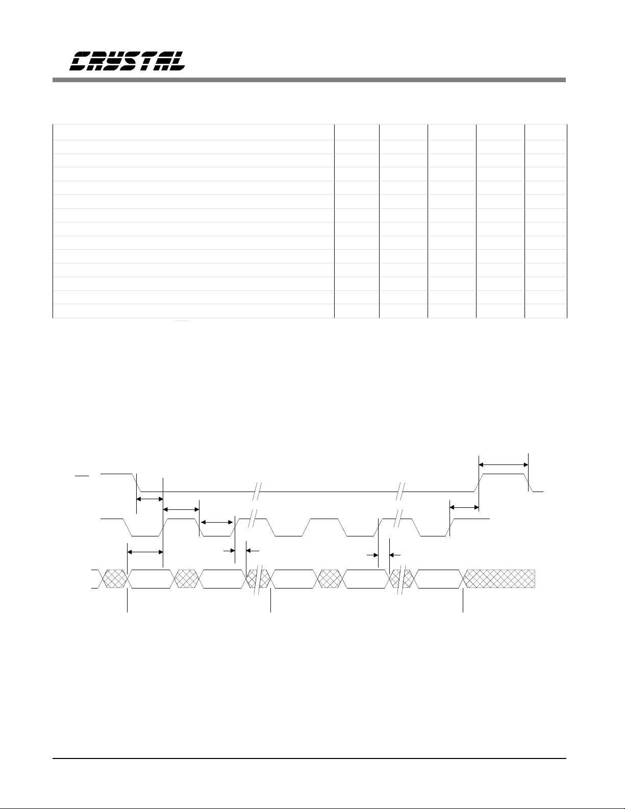
Figure 1. Recovered Clock and Data Switching Characteristics
6 DS40F2
CS61535A
E1 SWITCHING CHARACTERISTICS (TA = -4 0°C to 85 °C; TV+, RV+ = 5.0V ±5%;
GND = 0V; Inputs: Logic 0 = 0V, Logic 1 = RV+; See Figures 1, 2, & 3)
Parameter Symbol Min Typ Max Units
Crystal Frequency (Note 29) f
ACLKI Duty Cycle t
pwh3/tpw3
ACLKI Frequency (Note 30) f
RCLK Duty Cycle (Notes 31, 32) t
pwh1/tpw1
RCLK Cycle Width (Note 32) t
t
pwh1
t
RCLK Cycle Width (Note 32) t
t
pwh1
t
Rise Time, All Digital Outputs (Note 33) t
Fall Time, All Digital Outputs (Note 33) t
TPOS/TNEG (TDATA) to TCLK Falling Setup Time t
TCLK Falling to TPOS/TNEG (TDATA) Hold Time t
RPOS/RNEG Valid Before RCLK Falling (Note 34) t
RDATA Valid Before RCLK Falling (Note 35) t
RPOS/RNEG Valid Before RCLK Rising (Note 31) t
RPOS/RNEG Valid After RCLK Falling (Note 34) t
RDATA Valid After RCLK Falling (Note 35) t
RPOS/RNEG Valid After RCLK Rising (Note 31) t
TCLK Frequency f
TCLK Pulse Width (Notes 31, 34, 36, 37)
t
pwh2
(Notes 35, 36, 37)
c
aclki
pw1
pwl1
pw1
pwl1
r
f
su2
h2
su1
su1
su1
h1
h1
h1
tclk
- 8.192000 - MHz
40 - 60 %
-2.048-MHz
-29-%
310
90
120
320
-
100
488
140
348
488
348
140
670
190
500
670
- - 85 ns
- - 85 ns
25 - - ns
25 - - ns
100 194 - ns
100 194 - ns
100 194 - ns
100 194 - ns
100 194 - ns
100 194 - ns
-2.048-MHz
80
150
-
-
340
340
ns
ns
ns
ns
-
-
ns
ns
ns
ns
Any Digital Output
t
r
90% 90%
10%
10%
t
f
Figure 2. Signal Rise and Fall Characteristics
t
pw2
t
pwh2
TCLK
TPOS/TNEG
t
su2
t
h2
Figure 3a. Transmit Clock and Data Switching
t
ACLKI
Figure 3b. Alternate External Clock Characteristics
pwh3
t
pw3
Charact er ist ic s
DS40F2 7
SWITCHING CHARACTERISTICS (TA = -40 ° to 85°C; TV +, RV+ = ±5% ;
Inputs: Logic 0 = 0V, Logic 1 = RV+)
Parameter Symbol Min Typ Max Units
SDI to SCLK Setup Time t
SCLK to SDI Hold Time t
SCLK Low Time t
SCLK High Time t
SCLK Rise and Fall Time t
CS to SCLK Setup Time t
SCLK to CS Hold Time (Note 38) t
CS Inactive Time t
SCLK to SDO Valid (Note 39) t
CS to SDO High Z t
Input Valid To PCS Falling Setup Time t
PCS Rising to Input Invalid Hold Time t
PCS Active Low Time t
Notes: 38. For CLKE = 0,
CS must remain low at least 50 ns after the 16th falling edge of SCLK.
39. Output load capacitance = 50pF.
dc
cdh
cl
ch
, t
r
cc
cch
cwh
cdv
cdz
su4
h4
pcsl
f
50 - - ns
50 - - ns
240 - - ns
240 - - ns
- - 50 ns
50 - - ns
50 - - ns
250 - - ns
- - 200 ns
- 100 - ns
50 - - ns
50 - - ns
250 - - ns
CS61535A
CS
SCLK
SDI
t
t
t
dc
LSB
cc
ch
t
t
cdh
cl
LSB
CONTROL BYTE DATA BYTE
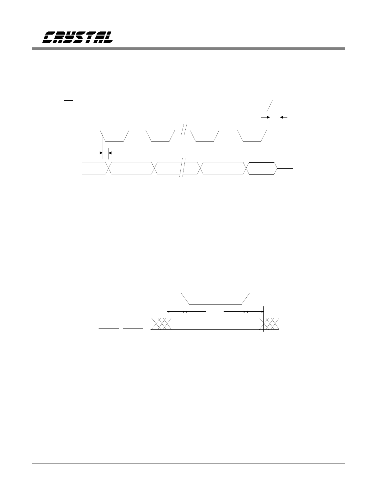
Figure 4. Serial Port Write Timing Diagram
t
cdh
MSB
t
cch
t
cwh
8 DS40F2
CS
SCLK
t
cdv
CS61535A
t
cdz
SDO
CLKE = 1
Figure 5. Seria l Port R ead Timi ng Di agra m
PCS
t
su4
t
LEN0/1/2, TAOS,
RLOOP, LLOOP,
RCODE, TCODE
Figure 6. Exte nded Ha rdwa re Mo de Par allel Chip Select Timin g Dia gram
VALID INPUT DATA
pcsl
t
h4
HIGH Z
DS40F2 9

CS61535A
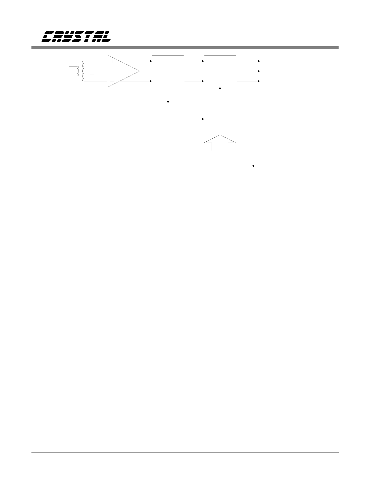
THEORY OF OPERATION
Enhancement s in CS61535 A
The CS61535A provides higher performance and
more features than the CS61535 including:
• 50% lower power consumption,
• Internally matched transmitter output imped-
ance for improved signal quality,
• Optional AMI, B8ZS, HDB3 enc oder/de cod er
or external line coding support,
• Receiver AIS (unframed all ones) detection,
• ANSI T1.231-1993 compliant receiver Loss
of Signal (LOS) handling,
• Transmitter TTIP and TRING outputs are
forced low when TCLK is static,
• The Driver Performance Monitor operates
over a wider range of input signal levels.
• Elimination of the requirement that a refer-
ence clock be input on the ACLKI pin.
Existing designs using the CS61535 can be converted
to the higher performance, pin-compatible CS61535A
if the transmit transformer is repl aced by a pin-compatible transform er with a new turns ratio and th e 4.4
Ω resistor use d in E1 75 Ω applications is shorted.
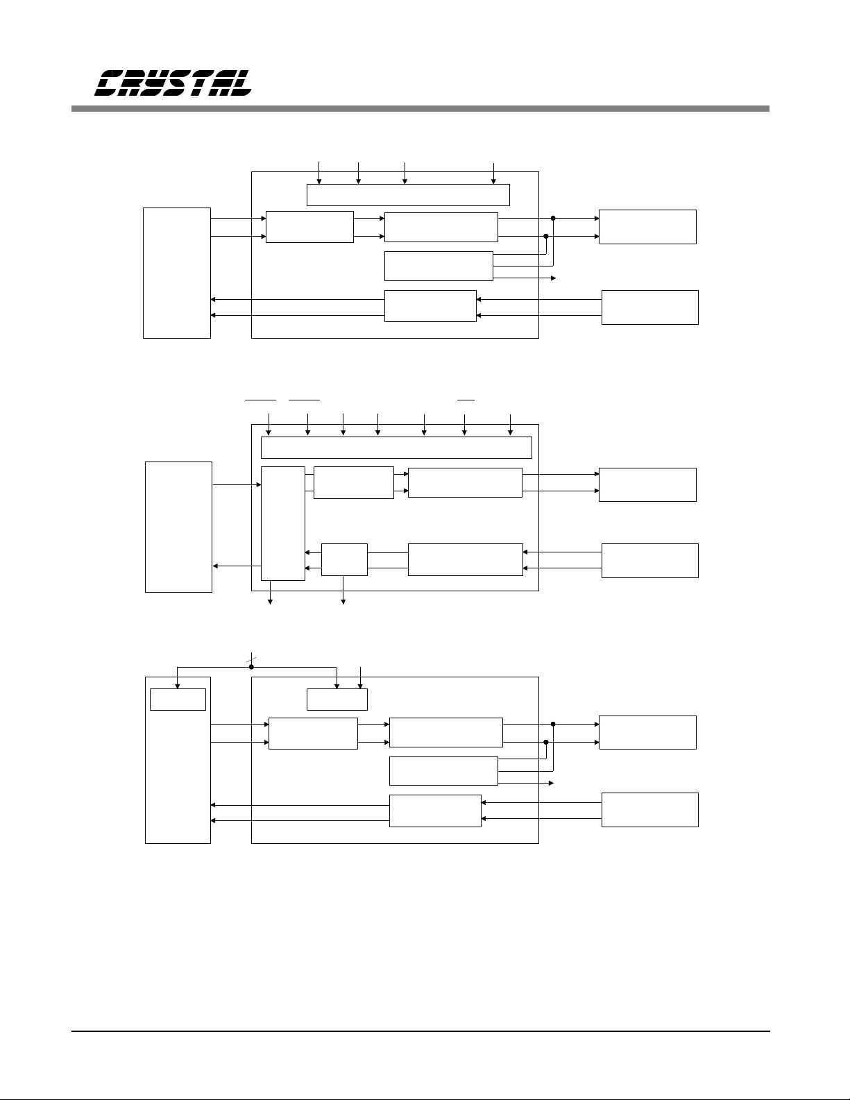
Introduction to Op erating Modes
The CS61535A supports three operating modes
which are se lected by th e level o f the MODE pi n
MODE
HARDWARE
MODE-PIN
INPUT LEVEL
CONTROL
METHOD
LINE CODE
ENCODER &
DECODER
AIS DETECTION NO YES NO
DRIVER
PERFORM-
ANCE MONITOR
<0.2V
INDIVIDUAL
CONTROL
LINES
NONE
YES NO YES
EXTENDED
HARDWARE
FLOAT, or
2.5V
INDIVIDUAL
CONTROL
LINES &
P ARALLEL
CHIP
SELECT
AMI,
B8ZS,
HDB3
HOST
>(RV+) - 0.2V
SERIAL
µ-PROCESSOR
PORT
NONE
as shown in Ta bles 1 and 2, Figure 7, and Figures
A1-A3 of the Applications section.
The CS61535A modes are Hardware Mode, Extended Hardware Mode, and Host Mode. In
Hardware and Extended Hardware Modes, discrete
pins are used to configure and monitor the device.
The Extended Hardware Mode provides a parallel
chip select input which latches the control inputs
allowing individual ICs to be configured using a
common set of control lines. In the Host Mode, an
external processor monitors and configures the device through a serial interface. There are thirteen
multi-function pins whose functionality is determined by the operatin g mode (se e Table 2).
Transmitter
The transmitter takes data from a T1 (or E1 ) terminal, attenuates jitter, and produces pulses of
appropriate shape. The transmit clock, TCLK,
and transmit data, TPOS & TNEG or TDATA, are
supplied synchronously. Data is sampled on the
falling edge of the input clock, TCLK.
Either T1 (DSX-1 or Network Interface) or E1
G.703 pulse shapes may be selected. Pulse sh aping and signal level are determined by "line
length select" inputs as shown in Table 3. The
MODE
FUNCTION PIN HARDWARE
TRANSMITTER
RECEIVER/DPM
CONTROL
3TPOS TDATATPOS
4TNEG
6 RNEG BPV RNEG
7 RPOS RDATA RPOS
11 DPM AIS DPM
17 MTIP
18 MRING - MRING
18 23 LEN0 LEN0
24 LEN1 LEN1 SDI
25 LEN2 LEN2 SDO
26 RLOOP RLOOP
27 LLOOP L LOO P SCLK
28 TAOS TAOS CLKE
EXTENDED
HARDWARE
TCODE TNEG
RCODE MTIP
PCS -
HOST
INT
CS
Table 1. Dif feren ces in Operat ing Mode s
Table 2. Pin Definitions
10 DS40F2
CS62180B
FRAMER
CIRCUIT
TNEG
RPOS
RNEG
JITTER
ATTENUATOR
CS61535A
EXTENDED HARDWARE MODE
HARDWARE MODE
RLOOP LEN0/1/2LLOOPTAOS
CONTROL
LINE DRIVER
DRIVER MONITOR
LINE RECEIVER
MRING
MTIP
TTIPTPOS
TRING
DPM
RTIP
RRING
CS61535A
TRANSMIT
TRANSFORMER
RECEIVE
TRANSFORMER
HIGH
SPEED
MUX
(e.g., M13)
CONTROL
CS62180B
FRAMER
CIRCUIT
TDATA
RDATA
BPV AIS
P SERIAL PORT
µ
5
TPOS
TNEG
RPOS
RNEG
RCODETCODE
AMI
B8ZS,
HDB3,
CODER
JITTER
ATTENUATOR
CS61535A
JITTER
ATTENUATOR
CS61535A
AIS
DETECT
CLKE
CONTROL
RLOOP PCS LEN0/1/2LLOOPTAOS
CONTROL
HOST MODE
LINE DRIVER
DRIVER MONITOR
LINE RECEIVER
LINE DRIVER
LINE RECEIVER
MRING
MTIP
TTIP
TRING
RTIP
RRING
TTIP
TRING
DPM
RTIP
RRING
TRANSMIT
TRANSFORMER
RECEIVE
TRANSFORMER
TRANSMIT
TRANSFORMER
RECEIVE
TRANSFORMER
Figure 7. Overv iew of Op eratin g Mode s
DS40F2 11
CS61535A
LEN2 LEN1 LEN0 OPTION SELECTED APPLICATION
0 1 1 0-133 FEET
100 133-266 FEET
101 266-399 FEET
110 399-533 FEET
111 533-655 FEET
001
0 0 0 CCITT G.703 2. 048 MHz E1
0 1 0 FCC Part 68, Option A CSU NETWORK
0 1 1 ANSI T1.403
AT&T C B113
(CS61535A only)
DSX-1
ABAM
(AT&T 600B
or 600C)
REPEATER
INTERFACE
Table 3. Line Length Selection
CS61535A line driver is desig ned to drive a 75 Ω
equivalent lo ad.
For T1 DSX-1 applications, line lengths from 0 to
655 feet (a s measured from t he transmitter to the
DSX-1 cross connect) are selectable. The five
partition arrangement meets ANSI T1.102-1993
requirements when using ABAM ca ble. A typical
output pulse is shown in Figure 8. These pulse
settings can also be used to meet CCITT pulse
shape requirements for 1.544 MHz operation.
width will meet the G.703 pulse shape template
shown in Fi gu r e 9, a n d specified in Table 4.
For E1 applications, the CS61535A driver provides 14 dB of return loss during the transmission
of both marks and spaces. This improves signal
quality by minimizing reflections off the transmitter. Similar levels of ret urn loss are provided
for T1 applications.
The CS61535A transmitter will detect a failed
TCLK, and will force the TTIP and TRING outputs low.
NORMALIZED
AMPLITUDE
1.0
0.5
AT&T CB 119
SPECIFICATION
For T1 Network Inte rface app lications , additi onal
options are provided. No te that the op timal pulse
width for Part 68 (324 ns) is narrower than the
optimal pulse width for DSX-1 (350 ns). The
CS61535A automatically adjusts the pulse width
based upon the "line length " se lection made.
The E1 G.703 pu lse shape is supported wit h line
length selection LEN2/1/0=0/0/0. The pulse
Nominal peak voltage of a mark (pulse) 2.37 V 3 V
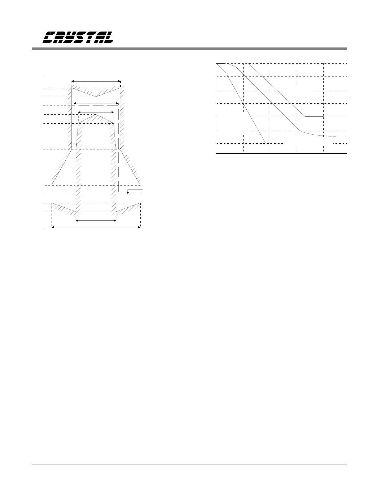
Peak voltage of a spac e (n o pulse)
Nominal puls e wi dt h 244 ns
Ratio of the amplitudes of positive and negative
pulses at the center of the pulse interval
Ratio of the widths of positive and negative
pulses at the nomi nal half amplitude
* When configured with a 0.47 µF nonpolarized capacitor in series with the TX transformer
primary as shown in Figures A1, A2 and A3.
0
CS61535A
OUTPUT
PULSE SHA PE
-0.5
0 250 750 1000
500
TIME (nanoseconds)
Figure 8. Typical Pulse Shape at DSX-1 Cross Connect
For coaxial cable,
75Ω load and
transformer specified
in Application Section.
For shielded twisted
pair, 120Ω load and
transformer specified
in Application Section.
0 ±0.237 V 0 ±0.30 V
0.95 to 1.05*
0.95 to 1.05*
Table 4. CCITT G.703 S pecificati ons
12 DS40F2
CS61535A
Percent of
nominal
peak
voltage
120
110
100
90
80
50
10
0
-10
-20
Figure 9 . Mask of the Pulse at the 2048 kbps Interface
269 ns
244 ns
194 ns
Nominal Pulse
219 ns
488 ns
When any transmit control pin (TAOS, LEN0-2
or LLOOP) is toggled, the transmitter stabilizes
within 22 bit periods. The transmitter will take
longer to stabilize when RLOOP is selected because the timi ng circuitry must adj ust to the new
frequency.
Jitter Attenuato r
The jitter attenu ator is designed to redu ce wander
and jitter i n the transmit clock signal. It c onsists
of a 32 bit FIFO, a cr ystal osci llator, a set of loa d
capacitors for the crystal, and cont rol logic. The
jitter attenuator exceeds the jitter attenuation requirements of Publications 43802 and REC.
G.742. A typical jitter attenuation curve is shown
in Figure 10.
The jitter attenuato r works in the following manner. Data on TPOS and TNEG (or TDATA) are
written into the jitter attenuator’s FIFO by TCLK.
The rate at which data is r ead out of th e F I FO and
transmitted is determined b y the oscillato r. Logic
circuits adju st the ca pacitive loadin g on the crys-
0
10
20
30
40
Attenuation in dB
b) Maximum
Attenuation
Limit
50
60
1 10 100 1 k 10 k
Figure 10. Typical Jitter Attenuation Curve
a) Minimum Attenuation Limit
AT&T 62 41 1
Requirem ents
Measure d P er formance
Frequenc y in H z
tal to set its oscillation frequency to the average
of the TCLK freque ncy. Signal jit ter is absorbed
in the FIFO.
Jitter Tolera nce of Jitter Attenuator
The FIFO in the jitter attenuator is designed to
neither overflow nor underflow. If the jitter amplitude becomes very large, the read and write
pointers may get very close together. Should the
pointers attempt to cross, the oscillator’s divide
by four circuit adj usts by performing a divide by
3 1/2 or divide by 4 1/2 to pre vent the overflow
or underflow. When a divide by 3 1/2 or 4 1/2
occurs, the data bit will be driven on to the line
either an eighth bit period early or an eighth bit
period late.
When the T CLK frequency is close to th e center
frequency of the crystal oscillator, the high frequency jitt er tolerance is 23 UI before the divide
by 3 1/2 or 4 1/2 circuitry is activated. As the
center frequency of the oscillator and the TCLK
frequency deviat e from one anoth er, the jitter tolerance is reduced. As this frequency deviation
becomes large, the maximum jitter tolerance at
high frequencies is reduced to 12 UI before the
underflow/overflow circuitry is activated. In application, it is unlikely that the oscillator center
frequency will be precisely aligned with the
DS40F2 13
CS61535A
1 : 2
RTIP
Data
Level
Slicer
RRING
Edge
Detector
Figure 1 1. Re cei ver Bl oc k Di agr am
TCLK frequency due to allowable TCLK tolerance, part to part variations, crystal to crystal
variations, and crystal temperature drift. The oscillator tends to trac k l ow freque ncy ji tter s o jitt er
tolerance increases as ji tter frequency decreases.
The crystal frequ ency must be 4 times the nominal signal frequen cy: 6.176 MHz for 1.544 MHz
operation; 8.192 MHz for 2.048 MHz applications. Internal capacitors load the crystal,
controlling the oscillation frequency. The crystal
must be des igned so that ove r operating temperature, the oscillator frequency range exceeds the
system frequ ency tole rance. Cry stal Semicondu ctor offers the CXT6176 & CXT8192 crystals,
which yield optimum performance with the
CS61535A.
Transmit All Ones Select
The transmitter provides for all ones insertion a t
the frequency of ACLKI. Transmit all ones is selected when TAOS goes high, and causes
continuous ones to be transmitted on the line
(TTIP and TRING). In this mode , the TPOS and
TNEG (or TDATA) inputs are ignored. A TAOS
request will be ignored if remote loopback is in
effect. ACLKI jitte r will be attenuated. TAOS is
Data
Sampling
&
Clock
Extraction
Clock
Phase
Selector
Continuously
Calibrated
Delay Line
RPOS
RNEG
RCLK
ACLKI or
Oscillator in Jitter
Attenuator
not available on the CS61535A when ACLKI is
grounded.
Receiver
The recei ver extracts da ta and clock f r om an AMI
(Alternate Mark Inversion) coded signal and outputs clock an d synchronize d data. The re ceiver is
sensitive to sign als over the entire range of cable
lengths and requires no equalization or ALBO
(Automatic L ine Build Out) c ircuits. The signal is
received on bot h ends of a center-tapped, centergrounded transformer. The transformer is
center-tapped on t he IC side. The clock and data
recovery cir cuit ex ceeds th e jitte r toleran ce specifications of Publications 43802, 43801, 62411
amended, TR-TSY-000170, and CCITT REC.
G.823.
A block diagram of the rec eiver is shown in Figure 11. The two leads of the transformer (RTIP
and RRING) have oppo site polarity allowing the
receiver to treat RTIP and RRING as unipolar signals. Comparators are used to detect pulses on
RTIP and RRING. The compara tor threshold s are
dynamically established at a percent of the peak
level (50% of peak for E1, 6 5% of peak for T1;
with the slicing level selected by LEN2/1/0).
14 DS40F2
CS61535A
The receiver us es an e dge detec tor and a con tinuously calibrated delay line to generate the
recovered clock. The delay line div ides its refer-
ence clock, ACLKI or the jitter attenuator’s
oscillator, into 13 equal divisions or phases . Continuous calib ration assures ti ming accuracy, even
if temperature or power supply voltage fluctuate.
The leading edge of an incoming data pulse triggers the clock ph ase selector. The phase selector
chooses one of the 13 avail able phases which th e
delay line pro duces for each bit perio d. The output from the phase selector feeds the clock and
data recovery circuits which generate the recovered clock and sample the incoming signal at
appropriate intervals to recover the data. The jitter
tolerance of the receiver exceeds that shown in
Figure 12.
300
100
28
PEAK
TO
10
PEAK
JITTER
(unit intervals)
1
.4
.1
Figure 12 . In put J itt er Tol eran ce of Receiv er
10 1k 10k0 100 100k700
JITTER FREQUENCY (Hz)
300
the Host Mode, CLKE determines the clock polarity for which output data is stable and valid as
shown in Table 5.
MODE
(pin 5)
LOW
(<0.2V)
HIGH
(>(V+) - 0.2V)
HIGH
(>(V+) - 0.2V)
MIDDLE
(2.5V)
X = Don’t care
Table 5. Data Ou tput/Cl ock Relati onship
CLKE
(pin 28)
XRPOS
LOW RPOS
HIGH RPOS
X RDA TA RCLK Falling
DATA CLOCK Clock Edge for
RNEG
RNEG
SDO
RNEG
SDO
RCLK
RCLK
RCLK
RCLK
SCLK
RCLK
RCLK
SCLK
Valid Data
Rising
Rising
Rising
Rising
Falling
Falling
Falling
Rising
Jitter and R ecovered Clock
The CS61535A are designed for error free clock
and data recovery from an AMI encoded data
stream in the presence of m o re than 0.4 unit intervals of jitter at high frequency. The clock
recovery circuit is also tolerant of long strings of
zeros. The edge of an incoming data bit causes
the circui try to choose a phase from the delay line
which most closely corresponds with the arrival
time of the data edge, and that clock phase triggers a pulse whi ch is typ ically 1 40 ns in d urat ion.
This phase of the delay line will continue to be
selected unt il a data bit a rrives which is clo ser to
another of the 13 phases, causin g a new phase to
be selected. The largest jump allowed along the
delay line is six phases.
The CS61535A outputs a clock immediately upon
power-up. The clock recovery circuit is calibrated, and the device will lock onto the AMI
data input immediately. If loss of signal occurs,
the RCLK frequency will equal the ACLKI frequency.
In the Hardware Mode , data at RPOS and RNEG
is stable and may be sampled on the rising edge
of the recovered clock. In the Exte nded Hardware
Mode, data at RDATA is stable an d may be sampled on the fallin g edg e of the recov ered clock . In
When an i nput signal is jitter free, the phase selection will occasionally jump between two
adjacent p hases resulting in RCLK jitte r with an
amplitude of 1/13 UIpp . These single phase
jumps are due to differences in frequ ency of the
incoming data and the calibration clock input to
ACLKI. For T1 operation of the CS61535A, the
instantaneou s period can be 14/1 3 * 648 ns = 698
ns (1,662,769 Hz) or 12/13 * 648 ns = 598 ns
(1,425,231 Hz) when adjacent clock phases are
chosen. As long as the s ame phase is c hosen, the
DS40F2 15

CS61535A
period will be 648 ns. Similar calculations hold
for the E1 rate.
The clock recove ry circuit is designed to accept at
least 0.4 UI of jitter at the rece iver. Since the data
stream contains information only when ones are
transmitted, a clo ck/dat a rec overy ci rcui t must assume a zero when n o signal is meas ured durin g a
bit period. Likewi se, when zeros are received, no
information is pres ent to update the clock reco very circuit regarding the trend of a signal which is
jittered. Th e result is that two ones that are separated by a string of zeros can exhibit maximum
deviation in pulse arrival time. For example, one
half of a period of jitter at 100 kHz occurs in 5
µs, which is 7. 7 T1 bi t p erio ds. If the j itt er ampl itude is 0.4 UI, then a one preceded by seven zeros
can have maximum displ acement in arrival time,
i.e. either 0. 4 UI too ea rly or 0.4 UI too late. For
the CS61535 A, the d ata recove ry circu it corre ctly
assigns a received bi t to its proper clock peri od if
it is displaced by less than 6/13 of a bit period
from its optimal location. Theoretically, this
would give a jitter tolerance of 0.46 UI. The actual jitter tolerance of the CS61535A is only
slightly less than the ideal.
In the event of a maximum j itter hit, the RCLK
clock period immediately adjusts to align itself
with the incom ing data and prepar e to accurately
place the next one, wheth er it arrives one p eriod
later, or after another string of zeros and is displaced by jitter. For a maximum early jitter hit,
RCLK will have a period of 7/13 * 648 ns = 34 9
ns (2,865,961 Hz). For a maxi mum late jitter hit,
RCLK will have a period of 19/ 13 * 648 ns = 947
ns (1,055,880 Hz).
Loss of Signal
Receiver loss of signal is indicated upon receiving 175 consecutive zeros. A digital counter
counts rece ived zeros based on RCLK cy cles. A
zero input is determine d eithe r when zeros ar e re-
ceived, or when the received signal amplitude
drops below a 0.3 V peak thres hold.
The receiver repo rts loss of signal by setting the
Loss of Signal pin, LOS, high . If the serial interface is used, the LOS bit will be set and an
interrupt issued on INT. LOS will go low (and
flag the INT pin again if serial I/O is used) wh en
a valid signal is detected. Note that in the Host
Mode, LOS is simultaneou sly available from both
the register and pin 12.
In a loss of signal state, the RCLK frequency will
be equal to the ACLKI freq uen cy sinc e ACL KI is
being used t o calibrat e the clock recovery circuit.
Received data is output on RPOS and RNEG (or
RDATA) regardless of LOS status. The LOS returns to lo gic zero when the ones density reaches
12.5% (based upon 175 b it periods starin g with a
one and cont aining less than 100 co nsecutive zeros) as prescribed in ANSI T1.231-1993. A
power-up or manual reset will also set LOS high.
Local Loopback
The local loopback mode takes clock and data
presented on TCLK, TPOS, and TNEG (or
TDATA) and outputs it at RCLK, RPOS and
RNEG (or RDATA). Local loopback is selected
by taking pin 27 high, or LLOOP may be selected
using the serial i nterface. The data on the transmitter inputs is transmitted on the line unless
TAOS is selected to cause the transmission of an
all ones signal instead. Receiver inputs are ignored when loc al loopback is in effect. Th e jitter
attenuator is not included in the local loopback
data path. Selection of local loopback overrides
the chip’s loss of signal response.
Remote Loopback
In remote loopback, the recove red clock and da ta
input on RTIP and RRING are sent through the
jitter attenuato r and back ou t on the lin e via TTIP
and TRING. Th e recovered inco ming signals are
also sent to RCLK, RPOS and RNEG (or
16 DS40F2

CS61535A
RDATA). Remote loopback is sel ected by taking
pin 26 high, or RLOOP may be selected using the
serial interface. Simultaneous selection of local
and remote l oopback modes is n ot valid (see R eset).
In the CS61535A Extended Hardware Mode, remote loopback occurs before the line code
encoder/decoder, insuring that the tran smitted signal matches the received signal, even in the
presence of received bipolar violations. The recovered data wil l also be decoded and outp ut on
RDATA if
RCODE is low.
Driver Performance Monitor
To aid in early detection and easy isolation of
nonfunctioning links, the Hardware and Host
Modes of the CS61535A are able to monitor
transmit drive performance and report when the
driver is no longer operational. This feature can
be used to monitor either the device’s performance or the performance of a neighboring dri ver.
The driver performance mon itor indicator is normally at a low (zero) l ogi c level , and g oes to hig h
level upon detecting driver failure. In the Host
Mode, DPM is available from both the register
and pin 11.
Line Code Encode r/Decoder
In Extended Hard ware Mode, three line code s are
available: AMI, B8ZS and HDB3. The input to
the encoder i s TDATA. The outputs from the decoder are RDATA and BPV (Bipolar Violation
Strobe). The enc oder and dec ode r are s elect ed u sing pins LEN2, LEN1, LEN0,
TCODE and
RCODE as shown in Ta ble 6.
LEN 2/1/0
000 010-111
TCODE
(Transmit
Encoder
Selection)
RCODE
(Receiver
Decoder
Selection)
Table 6. Selection of Encoder/Decoder
LOW
HIGH
LOW
HIGH
HDB3
Encoder
HDB3
Decoder
B8ZS
Encoder
AMI
Encoder
B8ZS
Decoder
AMI
Decoder
Alarm Indication Signal
In Extended Hardware Mode, the receiver sets the
output pin AIS high when less than 9 zeros are
detected out of 8192 b it period s. AIS returns low
when 9 or more zeros are detected out of 8192
bits.
The driver perf o r m ance monitor consi sts of an activity detect or that monit ors the trans mitte d signa l
when MTIP is connected to TTIP and MRING is
connected to TRING. DPM will go high if the
absolute difference between MTIP and MRING
does not transition above or below a threshold
level within a time-out period.
Whenever mor e than o ne line interface IC resi des
on the same circuit bo ard, the effectiven ess of the
driver perform ance moni tor can be maxi mized by
having each IC monitor performance of a neig hboring device, rather than having it monitor its
own performance.
Parallel Chip Select
In Extended Hardware Mod e,
gate the digital cont rol inputs :
PCS can be us ed to
TCODE, RCODE,
LEN0, LEN1, LEN2, RLOOP, LLOOP and
TAOS. Inputs are accepted on these pins only
when
PCS is low. Changes in inputs will imme diately change the operating state of the device.
Therefore, when cycling
PCS to update the operating state, the digital control inputs should be
stable for the entire
inputs are ignored when
PCS low period. The control
PCS is high.
Power On Reset / Reset
Upon power-up, the CS61535A is held in a static
state until the supply crosses a threshold of ap-
DS40F2 17

CS
SCLK
CS61535A
SDI
SDO
0
0 D7D6D5D4D3D2D1D0
Address/Command Byte
00 01 0R/W
Figure 13. Input/Output Timing
proximately three Volts. When this threshold is
crossed, the device will delay for about 10 ms to
allow the power supply to reach operating voltage.
After this delay, calibration of the delay lines used
in the transmit and receive sections commences.
The delay lines can be calibrated only if a reference clock is present. The reference clock for the
receiver is provided by ACLKI (or by the crystal
oscillator if ACLKI is not present). The reference
clock for the tra ns mitter is provided by TCLK. The
initial cali br ati on s h ould take less than 20 ms.
In operation, the delay lines are continuously calibrated, making the performance of the device
independent of power supply or te mperature va riations. The continuous calibration function
foregoes any requirement to reset the line interface when in opera tio n. However, a reset functio n
is available which will clear all registers.
In the Hardware and Extended Hardware modes, a
reset request is made by simultaneously setting both
RLOOP and LLOOP high for at least 200 ns. Reset
will initiate on the falling edge of the reset request
(falling edge of RLOOP and LLOOP). In the Host
Mode, a reset is initiated by simultaneously writing
RLOOP and LLOOP to the register. In either mode,
a reset will set all r egisters to 0 and s et LOS high.
Serial Interface
In the Host Mod e, pins 23 throug h 28 serve as a
microprocessor/microcontroller interface. One
eight-bit regi ster can be writt en t o via the SDI pin
or read from the SDO pin at the clock rate determined by SCLK. Through this register, a host
controller can be us ed to cont rol op erat ion al ch ar-
Data Input/Output
D6D5D4D3D2D1D0 D7
acteristics and monitor device status. The serial
port read/write timing is independent of the system transmit and receive timing.
Data transfer s are initiated by ta king the chip select input,
SCLK may be either high or low when
CS, low (CS must initially be high).
CS initially goes low. Address and input data bits are
clocked in on t he rising edge of SCLK. Data on
SDO is valid and stable on the falling edge of
SCLK when CLKE is low, and on the rising edge
of SCLK when CLKE is high. Data transfe rs are
terminated by setting
CS high. CS may go high
no sooner than 50 ns after the rising edge of the
SCLK cycle corresponding to the last write bit.
For a se rial data read,
CS may go high any time
to terminate the output.
Figure 13 shows th e timing relationship s for data
transfers whe n CLKE = 1. When CLKE = 0, da ta
output from the serial port, SDO, is v alid on the
falling edge of SCLK. For CLKE = 1, data bit D7
is held to the fallin g edge of the 16th clock cycle;
for CLKE = 0, data bit D7 is held to the rising
edge of the 17th c lock cycle. SDO goes to a high
LSB, first bit 0 R/W
1 ADD0 LSB of address, Must be 0
2 ADD1 Must be 0
3 ADD2 Must be 0
4 ADD3 Must be 0
5 ADD4 Must be 1
6 - Reserved - Must be 0
Table 7. Address/Command Byte
Read/Write Select; 0 = write, 1 =
read
18 DS40F2

CS61535A
impedance s tate either after bi t D7 is outp ut or at
the end of the hold period of data bit D7.
An address/command byte, shown in Table 7,
precedes a data register. The first bit of the address/command byte determines whether a read
or a write is requested . The next six bits contain
the address. The CS61535A responds to address
16 (0010000). The last bit is ignored.
The data r egister, shown in Table 8, can be written to the serial port. Data is input on the eight
clock cycles immediately following the address/command byte. Bits 0 and 1 are used to
clear an interrup t issued from the
INT pin, which
occurs in response to a loss o f signal or a problem
with the output dri ver. If bits 0 or 1 are tru e, the
corresponding int errupt is supp ressed. So if a loss
of signal inte rrupt is cleared by writing a 1 to bi t
0, the interrupt will be reenabled by writing a 0 to
bit 0. This holds for DPM as well.
LSB: first bit in 0 LOS Loss of Signal
1 DPM Driver Performance Monitor
2 LEN 0 Bit 0 - Li n e Length Sele c t
3 LEN 1 Bit 1 - Li n e Length Sele c t
4 LEN2 Bit 2 - Line Lenght Select
Table 9. Outp ut Data Bits 0 - 4
Bits
567
000
001
010
011
100
101
110
111
Reset has occurred or no program input.
TAOS in effect.
LLOOP in effect.
TAOS/L LOOP in effect.
RLOOP in effect
DPM changed st at e since last "clear DPM"
occured.
LOS chang ed state si nce last "clear LOS"
occured.
LOS and DPM have changed state since
last "clear LOS" and "clear DPM".
Stat us
LSB: first bit in 0 clr LOS Clear Loss of Signa l
1 clr DPM Clear Driver Performance Monitor
2 LEN0 Bit 0 - Line Length Select
3 LEN1 Bit 1 - Line Length Select
4 LEN2 Bit 2 - Line Lenght Select
5 RLOOP Remote Loopback
6 LLOOP Local Loopback
MSB: last bit in 7 TAOS Transmit All Ones Select
Table 8. Input Data Register
Writing a "1" to either "Clear LOS" or "Clear
DPM" over the serial interface has three effects:
1) the current interrupt on the serial interface
will be cleared . (Note that simply readi ng the
register bits will not clear the interrupt),
2) output data bits 5, 6 and 7 will be reset as
appropriate,
3) future interrupts for the c orresponding LOS
or DPM will be prevented from occurin g).
Table 10. Coding for Serial Output Bits 5, 6, 7
Writing a "0" to either "Clear LOS" or "Clear
DPM" enables the corresponding interrupt for
LOS or DPM.
Output data from the serial interface is p resented
as shown in Ta bles 9 and 10. Bits 2, 3 and 4 can
be read to verify line length selection. Bits 5, 6
and 7 must be decoded. Codes 101 , 11 0 and 111
(bits 5, 6 and 7) indicate LOS and DPM state
changes. Writing a "1" t o the "Clear LOS" and /or
"Clear DPM" bi ts in the regis ter also resets statu s
bits 5, 6, and 7.
SDO goes to a high i mpedance state when not in
use. SDO and SDI may be tied tog ether in applications where the host processor has a
bidirectional I/O port.
DS40F2 19

Power Supply
CS61535A
The device o perates from a sin gle +5 Volt su pply.
Separate pins for transmit and receive supplies
provide internal isolation. These pins should be
connected externally near the device and decoupled to their respective grounds. TV+ must not
exceed RV+ by more than 0.3V.
Decoupling and filtering of th e power suppl ies is
crucial for the proper opera tion of the analog circuits in both th e transmit and rec eive pat hs. A 1.0
µF capacitor should be connected between TV+
and TGND, and a 0.1 µF capacitor should be con-
nected between RV+ and RGND. Use mylar or
ceramic capacitors and place them as closely as
possible to their respective power sup ply pins. A
68 µF tantalum capacitor should be added close
to the RV+/RGND supply. Wire wrap breadboarding of the lin e interfac e is not rec ommende d
because lead resistance and inductance serve to
defeat the function of the decoupling capacitors.
Schematic & Layout Review Service
Confirm Optimum
Schematic & Layout
Before Building Your Board.
For Our Free Review Service
Call Applications Engineering.
Call:(512) 445-7222
20 DS40F2

PIN DESCRIPTIONS
CS61535A
Hardware Mode
ACLKI TAOS
TCLK LLOOP
TPOS RLOOP
TNEG LE N2
MODE LEN1
RNEG LEN0
RPOS RGND
RCLK RV+
XTALIN RRING
XTALOUT RTIP
DPM MRING
LOS MTI P
TTIP TRING
TGND TV +
1
2
3
4
5
6
7
8
9
10
11
12
13
14
ACLKI
28
27
26
25
24
23
22
21
20
19
18
17
16
15
TCLK TAOS
TPOS LLOOP
TNEG RLOOP
MODE LEN2
3272426281
RNEG LEN1
RPOS LEN0
RCLK RGND
XTALIN RV+
XTALOUT RRING
5
6
7
8
9
10
11
12 14 16 1813 15 17
top
view
25
24
23
22
21
20
19
DPM RTIP
LOS MRING
TTIP MTIP
TGND TRING
TV+
DS40F1 21

Extended Hardware M ode
CS61535A
ACLKI TAOS
TCLK LLOOP
TDATA RLOOP
TCODE L EN 2
MODE LEN1
BPV LEN0
RDATA RGND
RCLK RV+
XTALIN RRING
XTALOUT RTIP
LOS
TTIP TRING
TGND TV +
AIS
1
2
3
4
5
6
7
8
9
10
11
12
13
14
28
27
26
25
24
23
22
21
20
19
18
17
16
15
PCS
RCODE
ACLKI
TCLK TAOS
TDATA LLOOP
TCODE RLOOP
MODE LEN2
3272426281
BPV LEN1
RDATA LEN0
RCLK RGND
XTALIN RV+
XTALOUT RRING
5
6
7
8
9
10
11
12 14 16 1813 15 17
top
view
25
24
23
22
21
20
19
AIS RTIP
LOS
TTIP
PCS
RCODE
TGND TRING
TV+
22 DS40F1

Host Mode
CS61535A
ACLKI CLKE
TCLK SCLK
TPOS
TNEG SDO
MODE SDI
RNEG
RPOS RGND
RCLK RV+
XTALIN RRING
XTALOUT RTIP
DPM MRING
LOS MTI P
TTIP TRING
TGND TV +
1
2
3
4
5
6
7
8
9
10
11
12
13
14
ACLKI
28
27
26
25
24
23
22
21
20
19
18
17
16
15
CS
INT
TCLK CLKE
TPOS SCLK
TNEG
CS
MODE SDO
3272426281
RNEG SDI
RPOS
RCLK RGND
XTALIN RV+
XTALOUT RRING
5
6
7
8
9
10
11
12 14 16 1813 15 17
top
view
25
24
23
22
21
20
19
INT
DPM RTIP
LOS MRING
TTIP MTIP
TGND TRING
TV+
DS40F1 23

Power Supplies
RGND - Ground, Pin 22.
Power supply ground for all subcircuits except the transmit driver; typically 0 Volts.
RV+ - Power Supply, Pin 21.
Power supply for all subcircuits except the transmit driver; typically +5 Volts.
TGND - Ground, Transmit Driver, Pin 14.
Power supply ground for the transmit driver; typically 0 Volts.
TV+ - Power Supply, Transmit Driver, Pin 15.
Power supply for the transmi t driver; typically +5 Volts. T V+ must not e x ceed RV+ by more than
0.3 V.
Oscillator
XTALIN, XTALOUT - Crystal Connections, Pins 9 and 10.
A 6.176 MHz (or 8.192 MHz) cryst al should be connected acro ss these pins. If a 1.544 MHz (or
2.048 MHz) clock is provided on ACLKI (pin 1), the jitte r attenuator may be disabled by tyin g
XTALIN, Pin 9 to RV+ through a 1 kΩ resistor, and floating XTALOUT, Pin 10.
Overdriving the oscillator with an external clock is not supported.
CS61535A
Control
ACLKI - Alternate External Clock Input, Pin 1 .
The CS61535A does not re quire a clock signal to be input on ACLKI when a crystal is connected
between pins 9 and 10. If a clock is not provided on ACLKI, this input must be grounded. If
ACLKI is grounde d, the oscillato r in the jitter atte nuator is used to calibrate the clock recove ry
circuit and TAOS is not available.
CLKE - Clock Edge, Pin 28 . (Host Mode)
Setting CLKE to logic 1 causes RP OS and RNEG to be valid on the falling edge of RCLK, and
SDO to be v alid on the rising e dge of SC LK. Conversel y, setting CLKE to lo gic 0 cau ses RPOS
and RNEG to be valid on the rising edge of RCLK, and SDO to be valid on the falling edge of
SCLK.
CS - Chip Select, Pin 26. (Host Mode)
This pin must transition from high to low to read or write the serial port.
INT - Receive Alarm Interrupt, Pin 23. (Host Mode)
Goes low when LOS or DPM change state to flag the host processor.
"Clear LOS" or "Clear DPM" to th e register.
INT is an open drai n output and should b e tied to
the power supply through a resistor .
INT is cleared by writing
24 DS40F1

CS61535A
LEN0, LEN1, LEN2 - Line Length Selection, Pins 23, 24 and 25. (Hardware and Extended
Hardware Modes)
Determines the shape and amplitu de of the transmi tted pulse to acc ommodat e several cable types
and lengths. See Table 3 for information on line length selection. Also controls the receiver
slicing level and the line code in Extended Hardware Mode.
LLOOP - L ocal Loopback, Pin 27. (Hardware and Extended Hardware Modes)
Setting LLOOP to a logic 1 rout es the transmit clock and d ata through to the rec eive clock and
data pins. TPOS/TNEG (or TDATA) are still tra nsmitted unless overri dden by a TAOS request.
Inputs on RTIP and RRING are ignored.
MODE - Mode Select, Pin 5.
Driving the MODE pin high puts the CS61535A line interface in the Host Mode. In the host
mode, a serial control port is used to control the CS61535A line interface and determine its status.
Grounding the MODE pin puts the CS61535A line interface in the Hardware Mode, where
configuration and status are controlle d by discrete pins. Floa ting the MODE pin or driving it to
+2.5 V puts the CS61535A in Extended Hardware Mode, where configuration and status are
controlled by di screte pins. When floating MODE, there shoul d be no external load on the pin.
MODE defines the status of 13 pins (see T able 2).
PCS - Parallel Chip Select, Pin 18. (Extended Hardware Mode)
Setting
PCS high causes the CS61535A line interface to ignore the TCODE, RCODE, LEN0,
LEN1, LEN2, RLOOP, LLOOP and TAOS inputs.
RCODE - Receiver Decoder Select, Pin 17. (Extended Hardware Mode)
Setting
RCODE low enables B8ZS or HDB3 zero substitution in the receiver decoder. Setting
RCODE high enables the AMI receiver decoder (see Table 8).
RLOOP - Remote Loopba ck, Pin 26. (Hardware and Extended Hardware Modes)
Setting RLOOP to a logic 1 causes the recovered clock and data to be sent through the jitter
attenuator (i f active) and through th e driver back to the li ne. The rec overed signal is also sent to
RCLK and RPOS/RNEG (or RDA TA). Any TAOS request is ignored.
Simultaneously taking RLOOP and LLOOP high for at least 200 ns initiates a device reset.
SCLK - Serial Clock, Pin 27. (Host Mode)
Clock used to r ead or write the serial port registers. SCLK can be either high or low when the line
interface is selected using the
CS pin.
SDI - Serial Data Input, Pin 24. (Host Mode)
Data for the on-chip regis ter. Sampled on the rising edge of SCLK.
SDO - Serial Data Output, Pin 25. (Host Mode)
Status and contro l information from the on-chip register. If CLKE is high SDO is valid on the
rising edge of SCLK. If CLKE is low SDO is valid on the falling edge of SCLK. This pin goes to
a high-impedance sta te when the serial port is being written to or after bit D7 is outp ut.
DS40F1 25

CS61535A
TAOS - Transmit All Ones Select, Pin 28. (Hardware and Extended Hardware Modes)
Setting TAOS to a logic 1 causes c ontinuous o nes to b e transmitted at the frequen cy determine d
by ACLKI.
TCODE - Transmitter Encoder Select, Pin 4. (Extended Hardware Mode)
Setting
TCODE low enables B8Z S or HDB3 zero substituti on in the transmitter encod er. Setting
TCODE high enables the AMI transmitter encoder .
Data
RCLK - Recovered Clock, Pin 8.
The receiver recovered clock is output on this pin.
RDATA - Receive Data - Pin 7. (Extended Hardware Mode)
Data recovered from th e RTIP and RRING inputs i s outp ut a t this pin, a fter b ein g decode d by th e
line code decoder. RDATA is NRZ. RDATA is stable and valid on the falling edge of RCLK.
RPOS, RNEG - Receive Positive Data , Receive Negati ve Data, Pins 6 and 7. (Hardware and
Host Modes)
The receiver recovered NRZ dig ital data is output on th ese pins. In the Hardware Mode, RPOS
and RNEG are stabl e and valid on the ri sing edge of RCLK. In t he Host Mode, CLKE determin es
the clock edge for whi ch RPOS and RNEG are stable and valid. See Table 5. A positive pulse
(with respect to grou nd) received on the RTIP pin gene rates a logic 1 on RPOS, and a positive
pulse received on the RRING pin generates a logic 1 on RNEG.
RTIP, RRING - Receive Tip, Receive Ring, Pins 19 and 20.
The AMI receive signal is input to these pins. A center-tapped, center-grounded, 2:1, step-up
transformer is require d on these inputs, as shown in Figure A1 in the Appl ications secti on. Data
and clock are recovered and output on RCLK and RPOS/RNEG or RDATA.
TCLK - Transmit Clock, Pin 2.
The1.544 MHz (o r 2.048 MHz) tra nsmit clock is inp ut on this pin . TPOS/TNEG or TDATA are
sampled on the falling edge of TCLK.
TDATA - Transmit Data, Pin 3. (Extended Hardware Mode)
Transmitter NRZ input data whic h passes th rough th e line code encoder, and is then driven on to
the line through TTIP and TRING. TDATA is sampled on the falling edge of TCLK.
TPOS, TNEG - Transmit Positi ve Data, Tr ansmit Negative Data, Pins 3 and 4. (Hardware and
Host Modes)
Inputs for clock and data to be transmi tted. The signal is driven on to the li ne through TT IP and
TRING. TPOS and TNEG are sampled on the falling edge of TCLK. A TPOS input causes a
positive pulse to be transmitted, while a TNEG input causes a negative pulse to be transmitted.
TTIP, TRING - Transmit Tip, Transmit Ring, Pins 13 and 16.
The AMI signal is driven to th e lin e thro ugh thes e pi ns. In th e CS615 35A, this output is designe d
to drive a 75 Ω load. A 1:1, 1:1.15 or 1:1.26 transformer is required as shown in Figure A1.
26 DS40F1

CS61535A
Status
AIS - Alarm Indication Signal, Pin 11. (Extended Hardware Mode)
AIS goes high when unframed all-ones condition (blue alarm) is detected, using the detection
criteria of less than three zeros out of 2048 bit periods.
BPV- Bipolar Violation Strobe, Pin 6. (Extended H ardware Mode)
BPV strobes high when a bipolar violation is detected in the received signal. B8ZS (or HDB3)
zero su bstituti ons ar e not flag ged as bi polar vi olatio ns if th e B8ZS (or H DB3) dec oder has be en
enabled.
DPM - Driver Performance Monitor, Pin 11. (Hardware and Host Modes)
DPM goes high if no activity is detected on MTIP and MRING.
LOS - Loss of Signal, Pin 12.
LOS goes high when 175 consecutive zeros have been received. For the CS61535A, LOS returns
low when the ones density reaches 12. 5% (based upon 175 bit per iods startin g with a one and
containing less than 100 consecutive zeros) as prescribed by ANSI T1.231-1993.
MTIP, MRING - Monitor Tip, Monitor Ring, Pins 17 and 18. (Hardware and Host Modes)
These pins are normally connected to TTIP and TRING and monitor the output of a CS61535A.
INT pin in th e host m ode is us ed, and the m onitor is not use d, writing "Clear DPM" t o the
If the
serial interface will pre ven t an interru pt from the driver perform anc e monit or.
DS40F1 27
CS61535A
15
14
E1
28 pin
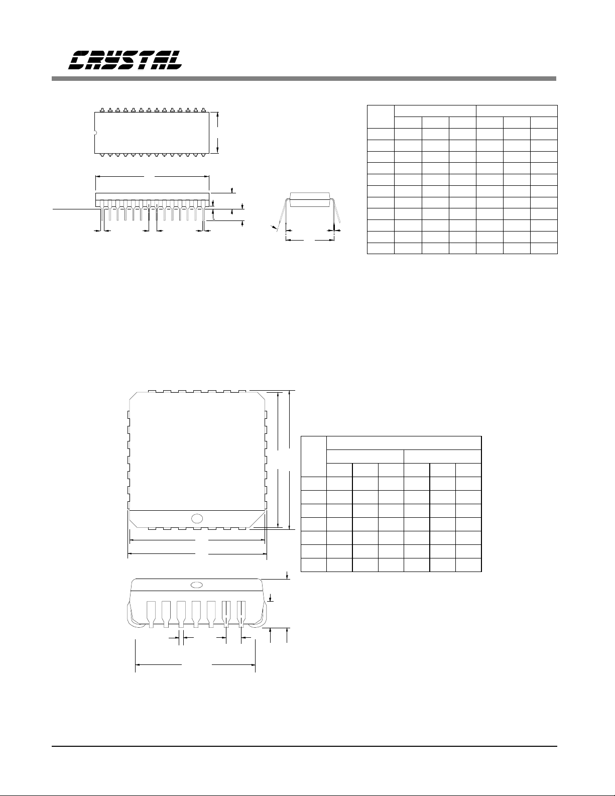
Plastic DIP
A
L
A1
B
∝
eA
SEATING
PLANE
B1
28
1
D
e1
NOTES:
1. POSITIONAL TOLERANCE OF LEADS SHALL BE WITHIN
0.25mm (0.010") AT MAXIMUM MATERIAL CONDITION, IN
RELATION TO SEATING PLANE AND EACH OTHER.
2. DIMENSION eA TO CENTER OF LEADS WHEN FORMED PARALLEL.
3. DIMENSION E1 DOES NOT INCLUDE MOLD FLASH.
28-pin PLCC
MILLIMETERS
DIM
MIN
3.94
A
A1
0.51
B
0.36
B1
1.02
0.20
C
36.45
D
E1
13.72
e1
2.41
eA
C
L
∝
15.24
3.18
0°
MAX
NOM
4.32
5.08
0.76
1.02
0.46
0.56
1.27
1.65
0.25
0.38
36.83
37.21
13.97
14.22 0.540
2.54
2.67 0.095
15.87 0.625
-
-
3.81
-
15°
INCHES
MIN MAX
NOM
0.200
0.170
0.155
0.040
0.030
0.020
0.022
0.018
0.014
0.065
0.050
0.040
0.015
0.010
0.008
1.465
1.450
1.435
0.560
0.550
0.105
0.100
0°
-
0.150
15°
-
0.600
0.125
28
E
E1
DIM
A1
D/E
D1
D
B
e
A1
D2/E2
D1/E1
D2/E2
A
MILLIMETERS INCHES
MAXMIN MAXMIN
NOM
A
2.29 0.090
B
12.32 12.57 0.485 0.495
11.43 11.58 0.450 0.456
9.91 10.92 0.390 0.430
e
1.19 1.35 0.047 0.053
4.574.20 0.1800.165
4.45
2.79
3.04 0.120
0.530.33 0.0210.013
0.41
12.45
11.51
10.41
1.27
NOM
0.175
0.110
0.016
0.490
0.453
0.410
0.050
28 DS40F1

APPLICATIONS
Monitor
Encoder/
Decoder
Control
&
Frame
Format
XTL
+
RV+
68 µF
RGND
28
1
12
11
5
7
6
8
3
4
2
9
10
CLKE
ACLKI
LOS
DPM
MODE
RPOS
RNEG
RCLK
TPOS
TNEG
TCLK
XTALIN
XTALOUT
+5V
0.1 µF
21 15
RV+ TV+
CS61535A
HOST
MODE
RGND TGND
IN
22 14
+
1.0 µF
TGND
SCLK
CS
INT
SDI
SDO
RTIP
RRING
MTIP
MRING
TRING
TTIP
27
26
23
24
25
19
20
17
18
16
13
+5V
100 k
R1
R2
0.47 µF
Ω
P
µ
Serial
Port
CT 2:1
CS61535A
RECEIVE
LINE
TRANSMIT
LINE
DEVICE FREQUENCY
MHz
1.544
CS61535A
2.048
2.048
Figure A1. Host Mode Configuration
Line Interface
Figures A1-A3 show the typical configurations
for interfacing the I.C. to a line through transmit
and receive transformers.
The receiver transformer is center tapped and
center grounded with resistors between the cent er
tap and e ach leg on th e I.C. side. These resistors
provide the termina tion for the line.
Figures A1-A3 show a 0.47 µF capacitor in series
with the transmit transformer primary. This capacitor is needed to prevent any buildup in the
CABLE
Ω
100
120
75
R1&2
Ω
200
240
150
Tr ansmit
Transformer
1:1.15
1:1.26
1:1
core of the transfor mer due to any DC imbalance
that may be present at the differential outputs,
TTIP and TRING. If DC saturates the transformer, a DC offset will result during the
transmissi on of a space (zero) a s the transformer
tries to dump the charge and return to equilibrium. The blocking capacitor will keep DC
current from flowing in the transformer.
Selecting an Oscil lator Crystal
Specific crystal parameters are required for
proper operation of the CS61535A. It is recommended that the CXT6176 from Crystal
DS40F2 29

CS61535A
+5V
+
68 µF
0.1 µF
+
1.0 µF
Control
&
Monitor
Frame
Format
Encoder/
Decoder
XTL
RGND
28
1
26
27
12
11
5
7
6
8
3
4
2
9
10
TAOS
ACLKI
RLOOP
LLOOP
LOS
DPM
MODE
RPOS
RNEG
RCLK
TPOS
TNEG
TCLK
XTALIN
XTALOUT
21 15
RV+ TV+
CS61535A
IN
HARDWARE
MODE
RGND TGND
22 14
TGND
LEN0
LEN1
LEN2
RTIP
RRING
MTIP
MRING
TRING
TTIP
23
24
25
19
20
17
18
16
13
Figure A2. Har dware Mo de Con figura tion
+5V
+
68 µF
0.1 µF
+
1.0 µF
Line
Length
Setting
R1
R2
0.47 µF
CT 2:1
RECEIVE
LINE
TRANSMIT
LINE
Control
&
Monitor
Frame
Format
Encoder/
Decoder
XTL
RGND
17
18
6
28
1
26
27
12
11
5
4
7
8
3
2
9
10
RCODE
PCS
BPV
TAOS
ACLKI
RLOOP
LLOOP
LOS
AIS
MODE
TCODE
RDATA
RCLK
TDATA
TCLK
XTALIN
XTALOUT
21 15
RV+ TV+
CS61535A
IN
EXTENDED
HARDWARE
MODE
RGND TGND
22 14
TGND
LEN0
LEN1
LEN2
RTIP
RRING
TRING
TTIP
23
24
25
19
20
16
13
Line
Length
Setting
CT 2:1
R1
R2
0.47 µF
Figure A3. Extended Hardware Mode Configuration
RECEIVE
LINE
TRANSMIT
LINE
30 DS40F2

CS61535A
Semiconductor be used for T1 applications, and
that the CXT8192 be used for E1 applications.
Interfacing The CS61 535A With the CS62180B
T1 Transceiver
To interface with the CS62180B, con nect the devices as shown in Figure A4. In this case, the
CS61535A and CS62180B are i n Host Mode controlled by a microprocessor serial interface. If the
CS61535A is used in Hardware Mode, then the
CS61535A RCLK output must be inverted before
being input to th e CS6 218 0B. If th e CS6 153 5A is
used in Extended Hardware Mode, the CS61535A
RCLK output do es not ne ed to be inv erted before
being input to th e CS62180B.
TO HOST CONTROLLER
V+
0.1uF
100k
V+
22k
68uF
+
SCLK
SDO
SDI
CS
CS62180B
TCLK
TPOS
TNEG
RNEG
RPOS
RCLK
1.544 MHz
CLOCK
SIGNAL
V+
100k
ACLKI
TCLK
TPOS
TNEG
MODE
RNEG
RPOS
RCLK
CS61535A
CLKE
SCLK
SDO
SDI
INT
RGND
RV+
CS
0V
+5V
ing appli cations where eight bi ts can be dropped
from the clock/data stream at once. Similarly,
these parts can be used in SONET applications
with the additi on of some external circuit ry.
The main differences of the CS61535A relative
to the CS61534 is:
1) On the CS61535A, selection of LEN 2/1/0 =
0/0/0 changes the voltage at which the receiver
accepts an input as a pulse (slicing level) from
65% to 50% of the pea k pulse amplit ude. Lowering the data slicing level will improve receiver
sensitivity at long cable lengths whe n the data is
jittered. A 50% slicing level will also improve
crosstalk sensitivity for channels where received
pulses do not have undershoot.
2) There are differences in the functionality of the
ACLKI (ACLK) input on the CS61534 and
CS61535A. ACKLI (ACL K) is used as the tran smit clock in the transmit all ones (TAOS) mode .
On the CS61535A, ACLKI is used as a calibration reference for the receiver clock recovery
circuit and therefore may not be supplied by
RCLK. On the CS61 534 , ACL K may be sup pli ed
by RCLK . If an external clock is not provide on
the ACLKI input of the CS61535A, the crystal
oscillator is used to calibrate the receiver clock
recovery circuit.
3) On the CS61535A, the Host Mode status regis-
Figure A4. Interfacing the CS61535A with the
CS62180B (Host Mode)
ter bits 5, 6 and 7 are encoded so that state
changes on LOS and DPM may be reported.
4) RCLK on th e CS61534 has a 50% dut y cycle,
CS61534 Compatibility
while RCLK on the CS61535A has a duty cycle
which is typically 30% or 70%. Also, the
The CS61535A is pin compatible with the
CS61534. The CS6 1535A has greater jitter tolerance for both transmitter and receiver, and it
provides more jitter attenuation starting at jitter
CS61535A RCLK duty cycle and instantaneous
frequency vary with received jitter and may exhibit 1/13 UIp p quantization jitter eve n when the
incoming sign al is jitter free.
frequencies of 6 Hz. The greater jitter tolerance
and attenuation in the transmit path makes the
CS61535A more suitable for CCITT demultiplex-
5) The CS61 535A requires 25 ns of setu p time on
TPOS and TNEG before the falling edge of
TCLK and 25 ns of hold time on these inputs af-
DS40F2 31

CS61535A
ter the falling edge of TCLK. The CS61534 requires 50 ns of hold time on TPOS and TNEG
after the falling edge of TCL, and 0 ns of setup
time.
6) LOS occurs after 31 consecut ive zeros on the
CS61534. For the CS61535A LOS occurs after
175 zeros.
7) Since the CS61535A receivers are continuously calibrated , there is no need to issue a reset
to initialize the receiver timing as with the
CS61534.
Using the CS61535A fo r SONET
The CS61535A can be applied to SONET VT1.5
and VT2.0 interface circuits as shown in Figure A5. The SONET data rat e is 51.84 MHz, and
has 6480 bits per frame (125 us per frame). An
individual T1 frame (193 bits pe r frame) or PCM-
30 frame (256 bits per frame) has its data mapped
into the 6480 bit SONET frame. The mapping
does not result in a uniform spacing between
sucessive T1 (or E1) bits. Rather, for locked VT
applications , gaps as la rge as 24 T1 bit periods or
32 E1 bit periods can exist between successive
bits. With floating VTs, the gaps can be even
larger.
The circuit in Figure A5 eliminates the demultiplexing jitter in a two-step approach. The first
step uses a FIFO which is filled at a 51.84 MHz
rate (when T1 or E1 bits are present), and which
is emptied at a sub-multiple of the 51.84 rate. The
FIFO is emptied only when it contains data.
When the FIFO is empty th e output clock is not
pulsed.
The sub-multiple rate chosen should be slightly
faster than the target rate (1.544 or 2.048 MHz),
but as close to the target rate as possible. For
6480 to
193 bit
(or 256 bit)
Mapping
Circuit
TCLK1
TSER
RSER
RCLK1
51.84 MHz
Empty
FIFO
FIFO
Div By
Write
Clock
TSER
CS62180B
RSER
RCLK2
Figure A5. SONET Application
TCLK2
TPOS
TNEG
RPOS
RNEG
RCLK2
Jitter
Attenuator
Driver
CS61535A
Receiver
32 DS40F2

CS61535A
locked VT operation, Table A1 shows potential
sub-multiple data rates, and the impact on those
rates on the maximum gap in th e output clo ck of
the FIFO, and depth of FIFO required. FIFO
depth will have to be increased for floating VT
operation, with 8 bit s of FIFO depth being added
for each pointer alignment change that can occur .
The objective that should be met in picking a
FIFO depth and clock divider is keep the maximum gap on the output of the FIFO at 12 bits or
less. Twelve bits is the maximum ji tter which ca n
be input to th e CS61535A’s jitter attenuator without causing the overflow/undeflow protection
circuit to operate. The CS61535A then removes
the remaining jitter from the signal.
The receive path also requires a bit mapping
(from 193 or 256 bits to 6480 bit s). This mapping
requires an input buffer with the same depth as
use on the trans mit path. This bu ffer also absorbs
the output jitter generated by the CS61535A’s
digital clock recovery.
Transformers
Recommended transmitter and receiver transformer specifications for the CS61535A are
shown in Table A2. The transformers in Ta ble A3
have been tested and recommended for use with
the CS61535A. Refer to the "Telecom Transformer Selection Guide" for detailed schematics
which show how to connect the lin e interface IC
with a particular transformer.
In applicat ions with the C S 61535A where it is advantageous t o u se a si ngl e tr ansmitt er t rans form er
for both 75 Ω and 120Ω E1 applicat ions, a 1: 1.26
transforer may be used. Although transmitter re-
turn loss will be reduced for 75Ω applications, the
pulse amplitude will be correct across a 75 Ω
load.
Target Rate
(MHz)
1.544 32 1.620 6.2 10 21
1.544 33 1.571 3.9 6 26
2.048 25 2.074 3.4 7 34
Parameter CS61535A Receiver CS61535A Transmitter
Turn s R at i o
Primary Inducta nce
Primary Leakage Inductance
Secondary Leakage Inductance
Interwindin g C apacitance 23 pF max. 18 pF max.
ET- constant
Clock
Divider
Resultant
Rate (MHz)
Table A1. Locked VT FIFO Analysis
1:2 CT ± 5% 1:1 ± 1.5 % for 75 Ω E1
600 µH min. @ 772 kHz
1.3 µH max. @ 772 kHz 0.3 µH max. @ 77 2 kH z
0.4 µH max. @ 772 kHz 0.4 µH max. @ 77 2 kH z
16 V-µs min. for T1
12 V-µs min. for E1
Maximum Gap FIFO Depth
(µs)
bits
Required
1:1.15 ± 5 % for 100 Ω T1
1:1.26 ± 1.5 % for 120 Ω E1
1.5 mH min. @ 77 2 kH z
16 V- µs min. for T1
12 V-µs min. for E1
Table A2. Transformer Specifications
DS40F2 33

CS61535A
Application Turns
Ratio(s)
RX:
T1 & E1
TX:
T1
TX:
E1 (75 & 120 Ω)
RX &TX:
T1
RX &TX:
E1 (75 & 120 Ω)
RX &TX:
T1
RX &TX:
E1 (75 & 120 Ω)
RX :
T1 & E1
TX:
E1 (75 & 120 Ω)
1:2CT Pulse Engineerin g PE-65351 1.5 kV through- hol e, single
1:1.15 Pulse Engineering PE-65388 1.5 kV through-hole, single
1:1.26
1:2CT
1:1.15
1:2CT
1:1.26
1:2CT
1:1.15
1:2CT
1:1.26
1:2CT Pulse Engineerin g PE-65835 3 kV through-hole, single
1:1.26
1:1
1:1
1:1
1:1
Manufacturer Part Number Package Type
Schott 67129300
Bel Fuse 0553-0013-HC
Schott 67129310
Bel Fuse 0553-0013-RC
Pulse Engineerin g PE-65389 1.5 kV through-hole, single
Schott 67129320
Bel Fuse 0553-0013-SC
Pulse Engineerin g PE-65565 1.5 kV through-hole, dual
Bel Fuse 0553-0013-7J
Pulse Engineerin g PE-65566 1.5 kV through-hole, dual
Bel Fuse 0553-0013-8J
Pulse Engineerin g PE-65765 1. 5 kVs ur fa ce-m ount, dual
Bel Fuse S553-0013 -0 6
Pulse Engineerin g PE-65766 1.5 kV surf ace-mount, dual
Bel Fuse S553-0013 -0 7
EN60950, EN41003 approved
Pulse Engineerin g PE-65839 3 kV through-hole, single
EN60950, EN41003 approved
Table A3. Recommended Transformers For The CS61535A
34 DS40F2

CDB61534, CDB61535, CDB61535A, CDB6158,
CDB6158A, CDB61574, CDB61574A, CDB61575,
CDB61577, CDB615304A, & CDB61305A
Line Interface Evaluation Board
Features
Socketed Line Interface Device
•
All Required Components for Complete
•
Line Interface Evaluation
Configuration by DIP Switch or Serial
•
Interface
LED Status Indicators for Alarm
•
Conditions
Support for Host, Hardware, and
•
Extended Hardware Modes
Mode Select
Circuit
General Description
The evaluation board includes a socketed line interface
device and all support components necessary for
evaluation. The board is powered by an external 5 Volt
supply.
The board may be configured for 100 Ω twisted-pair
T1, 75 Ω coax E1, or 120 Ω twisted-pair E1 operation.
Binding posts are provided for line connections. Several BNC connectors are available to provide system
clocks and data I/O. Two LED indicators monitor device alarm conditions. The board supports all line
interface operating modes.
ORDERING INFORMATION:
CDB61534, CDB61535. CDB61535A,
CDB6158, CDB6158A, CDB61574,
CDB61574A, CDB61575, CDB61577,
CDB61304A, CDB61305A
+5V 0V
Serial Interface
Control Circuit
Control Circuit
ACLKI
TCLK
TPOS
(TDATA)
TNEG
(TCODE)
RCLK
RPOS
(RDATA)
RNEG
(BPV)
Reset
Circuit
Hardware
LED Status
Indicators
CS61534,
CS61535,
CS61535A,
CS6158,
CS6158A,
CS61574,
CS61574A,
CS61575,
CS61577,
CS61304A
or
CS61305A
TTIP
TRING
RTIP
RRING
XTL
Crystal Semiconductor Corporation
P.O. Box 17847, Austin, TX 78760
(512) 445-7222 FAX: (512) 445-7581
SEP ’95
DS40DB3
35

LINE INTERFACE EVALUATION BOARD
POWER SUPPLY
As shown on the evaluation board schematic in
Figure 1, power is supplied to the evaluation
board from an exter nal +5 Volt sup ply connected
to the two b inding posts labeled +5V and GND.
Transient suppressor D10 protects the components on the boa rd from over-volt age damag e an d
reversed supply connections. The recommended
power supply decoupling is provided by C1, C2
and C3. Ceramic cap acitor C1 and electrolytic capacitor C2 are used to decouple RV+ to RGND.
Capacitor C3 decouples TV+ t o TGND. The TV+
and RV+ power sup p ly traces are connected at th e
device socket U1. A ground plane on the component side of the evaluation board insures optimum
performance.
BOARD CONFIGURATION
Pins on line interface device U1 with more than
one pin name hav e different functions dependin g
on the operating mode selected. Pin names not
enclosed in parenthesis or square brackets describe the Hardware mode pin function. Pin
names enclosed in parenthesis describe the Extended Hardware mode pin function. Pin names
enclosed in square brackets describe the Host
mode pin function.
Table 1 explains how to configure t he evaluation
board jump ers depending on the devic e installed
and the desired operating mode. Mode selection
is accompli shed with slide switch SW1 and jump ers JP2, JP6, and JP7. The CS61535A,
CS61574A, CS615 75, CS615 77, CS61304A, and
CS61305A support the Hardware, Extended
Hardware, and Host operating modes. The
CS61534, CS61535, and CS61574 support the
Hardware and Host operating modes. The
CS6158 and CS6158A only support the Hardware
operating mode.
Hardware Mode
In the Hardware operating mode, the line interface is config ured usin g DIP switch S2. The di gital control input s to the device selected by S2 include: transmit all ones (TAOS), local loopback
(LLOOP), remote loopback (RLOOP), and tran smit line length selection (LEN2,LEN1,LEN0).
Closing a DIP switch on S2 towa rds the lab el set s
the device control pin of the same name to logic 1
(+5 Volts). Note that S2 switch po sitions
and
RCODE have no function in Hardware mode.
TCODE
In additi on, the host processor interface connector
JP1 should not be used in the Hardware mode.
Tw o LED status indicators are provid ed in Hardware mode. The LED labeled DPM (AIS) illuminates when the line interface asserts the Driver
JUMPER POSITION FUNCTION SELECTED
JP1 - Connector for external pro cessor in Host operating mo de.
JP2, JP6, JP7
JP3
JP4
JP5
JP8
36 DS40DB3
A-A Extended Hardware operating mode.
B-B Hardware or Host operati ng modes.
IN Hardware or Extended Hardw are operating modes.
OUT Host operating mode.
C-C Connects the ACLKI BN C input to pin 1 of devic e.
D-D
E-E Transmit line connection for all applications exce pt those listed for "F-F" on the next line.
F-F
IN Shorts resistor R2 for all applications exce pt those listed for "OUT" on the next line.
OUT
Grounds the ACLKI BNC input through 51
75
Ω coax E1 appl i cations using the Schott 12932/12532 or PE-65389/65566 at transformer T1.
Inserts resistor R2 for 75
Table 1. Evaluation Board Jumper Settings
Ω coax E1 appli cations usi ng the CS61534, 35, 58, 74, or 77.
Ω resistor R1.

LINE INTERFACE EVALUATION BOARD
R15
100
RV+
+5V
D10
CC
Pin 4
ACLKI
R17
10k
P6KE
6
8
2
3
7
1
4
23
24
25
26
27
28
R14
4.7k
SIP
MODE
MODE
SW1
Ω
RNEG (BPV)
RCLK
TCLK
TPOS (TDATA)
RPOS (RDATA)
ACLKI
TNEG (TCODE)
LEN0 [INT]
LEN1 [SDI]
LEN2 [SD0]
RLOOP [CS]
LLOOP [SCLK]
TAOS [CKLE]
511
Ω
GND
(0V)
R1 51.1
Ω
JP2
BB
D8
C4 0.047µF
6
R16
1k
Ω
Pin 6
RCLK
TCLK
Pin 3
Pin 7
JP4
DD
AA
3
R18
10k
Ω
RNEG
(BPV)
RCLK
TCLK
TPOS
(TDATA)
RPOS
(RDATA)
RV+
ACLKI
Ω
TNEG
S2
RCODE
TCODE
LEN0/INT
LEN1/SDI
LEN2/SD0
RLOOP/CS
LLOOP/SCLK
TAOS/CLKE
INT
SDI
SDO
CS
SCLK
D9
JP1
1N914
S1
RESET
R4
221k
Ω
875124
RV+
C2
F
0.1
µ
C3
F
1
µ
{CS6158/58A: RT}
{CS6158/58A: NC}
U1
RV+
DPM
(AIS)
HOST:3-1,6-8
EXT HW: 3-2, 6-7
HW: 3-4, 6-5
C1
68
µ
F
+
221415
21
RV+TV+ TGND RGND
XTALIN
XTALOUT
RTIP
RRING
TTIP
MRING (PCS)
TRING
MTIP (RCODE)
LOSDPM (AIS)MODE
12
LOS
Q2
2N2222
LED
D2
R5
Ω
470
Prototyping
Area
RV+
R13 (only included for CS6158/58A)
1k
Ω
9
E1: CXT8192
T1: CXT6176
(not included for CS6158/58A)
10
RV+
RTIP
19
RRING
20
13
Pin 18
18
TRING
16
Pin 17
17
2N2222
Q1
LED
R6
470
D3
Change R9 and R10 for E1 operation
R10
200
Ω
R9
200
Ω
TTIP
JP6
BB
AA
JP7
BB
AA
(Used only for E1 75
applications with the CS61534,
CS61535, CS6158, CS61574,
OR CS61577)
Ω
(see Table 2)
0.47 µF
C5
JP8
R2
4.4
Ω
CS61534, CS61535,
U1:
CS61535A, CS6158,
CS6158A, CS61574,
CS61574A, CS61575,
CS61577, CS61304A,
OR CS61305A
RV+
T2
2:1
JP5
FF
T1
(see Table 2)
Ω
RTIP
RRING
TTIP
EE
TRING
Figure 1. Evaluation Board Schematic
DS40DB3 37

LINE INTERFACE EVALUATION BOARD
Performance Monitor alarm. The LED labeled
LOS illuminates when the line interface receiver
has detected a loss of sign al.
Extended Hardware Mode
In the Extended Hardware operating mode, the
line interface is configured using DIP switch S2.
The digital control inputs to the device selected
by S2 include: transmit all ones (TAOS), local
loopback (LLOOP), remote loopback (RLOOP),
transmit line length selection (LEN2, LEN1,
LEN0), transmit line code (
line code (
RCODE). Closing a DIP switch (mov-
TCODE), and receive
ing it towards the S2 la bel) sets the device control
pin of the same name to logic 1 (+5 Volts ). Note
that the
TCODE and RCODE options are active
low and are enabled when the switch is moved
away from the S2 label. The parallel chip select
input
PCS is tied to ground in Extended Hardware mode to enable the device to be reconfigured when S2 is changed. In addition, the host
processor interface connector JP1 should not be
used in Extended Hardware mode.
Two LED status indicators are provided in Extended Hardware mode. The LED labeled DPM
(AIS) illuminates when the line interface detects
the receive blue alarm (AIS). The LED labeled
LOS illuminates when the line interface receiver
has detected a loss of sign al.
Host Mode
In the Host operating mode, the line interface is
configured using a host processor connected to
the serial interface por t JP1. Th e S2 switch posi tion labeled CLKE selects the active edge of
SCLK and RCLK. Closing the CLKE switch s elects RPOS an d RNEG to be valid o n the falling
edge of RCLK an d SDO to be valid on the rising
edge of SCLK as required by the CS2180B T1
framer.
All other DIP switch positions on S2 should be
open (logic 0 ) to preve nt shortin g of the seri al in-
terface signals. Resistor R15 is a current limiting
resistor that prevents the serial interface signals
from being sh orted directly to th e +5 Vol t supply
if any S2 switch, other than CLKE, is closed.
Jumper JP3 should be out so the
INT pin may be
externally pulled-up at the host processor interrupt pin.
Two LED status indicators are provided in Host
mode. The LED labeled DPM (AIS) illuminates
when the line interface asserts the Driver Performance Monitor alarm. The LED labeled LOS
illuminates when the line interface receiver has
detected a loss of signal.
Manual Reset
A manual reset circuit is provided that can be
used in Hardware and Extended Hardware
modes. The reset circ uit consists of S1, R4, R16,
C4, D8, and D9. Pressing switch S1 forces both
LLOOP and RLOOP to a logic 1 and causes a
reset. A reset is only neces sary for the CS615 34
device to calibra te the center frequency of the receiver clock reco very circuit. All ot her line interface units use a co ntinuously calibrat ed clock recovery circuit that eliminates the reset requirement.
TRANSMIT CIRCUIT
The transmit clock and data signals are supplied
on BNC inputs labeled TCLK, TPOS(TDATA),
and TNEG. In the Hardware and Host operating
modes, data is supplied on the TPOS(TDATA)
and TNEG connectors in dual NRZ format. In the
Extended Hardware op erating mode, data is supplied in NRZ format on t he TPOS(TDATA) connector and TNEG is not used.
The transmitter output is transformer coupled to
the line through a transformer denoted as T1 in
Figure 1. T he signal is availa ble at the TTIP and
TRING binding pos ts. Capaci tor C5 is the reco mmende d 0. 47
µF DC blocking capacitor.
38 DS40DB3

LINE INTERFACE EVALUATION BOARD
The evaluat ion board su pports 100Ω twiste d-pair
T1, 75Ω coax E1, and 120Ω twisted-pair E1 o p-
eration. The CDB61534, CDB61535, CDB6158,
CDB61574, and CDB61577 are supplied from
the factory with a 1:2 transmit transformer that
may be used fo r all T1 and E1 applicat ions. The
CDB61535A, CDB6158A, CDB61574A,
CDB61575, CDB61304A, and CDB61305A are
supplied with a 1:1.15 transmit transformer installed for T 1 applications. An additional 1:1:1.26
transformer for E1 applications is provided with
the board. This transformer requires JP5 to be
jumpered across F-F for 75Ω coax E1 applications.
The CDB61534, CDB61535, CDB6158,
CDB61574, and CDB61577 require the JP8
jumper to be out for 75Ω coax E1 applications.
This inserts resistor R2 to reduce the transmit
pulse amplitude and meet the 2.37 V nominal
pulse amplitude requirement in CCITT G.703. In
addition, R2 increases the eq uivalent lo ad impedance across TTIP and TRING.
The recovered clock and data signals are available on BNC outputs labeled RCLK,
RPOS(RDATA), and RNEG(BPV). In the Hardware and Host opera ting modes, data is outpu t on
the RPOS(RDATA) and RNEG(BPV) connectors
in dual NRZ format. In the Extended Hardware
operating mode, data is output in NRZ format on
the RPOS(RDATA) connector and bipolar violations are reported on the RNEG(BPV) connector.
QUARTZ CRYSTAL
A quartz crystal must be installed in socket Y1 for
all devices except the CS6158 and CS6158A. A
Crystal Semiconductor CXT6176 crystal is recommended for T1 operation and a CXT8192 is
recommended for E1 operation. The evaluation
board has a CXT6 176 installe d at the factory a nd
a CXT8192 is also provided with the board.
The CDB6158 and CDB6158 A have resistor R13
installed instead of a crystal. This connects the RT
pin of the device to the +5 Volt supply.
RECEIVE CIRCUIT
The receive line interface signal is input at the
RTIP and RRING binding posts. The receive signal is trans f orm er coupled to the line interface device through a center-tappe d 1:2 transforme r. The
transformer produces ground referen ced pulses of
equal amplitude and opposite polarity on RTIP
and RRING.
The receive li ne interface is terminate d by resistors R9 and R10. The evalua tion boards are sup-
plied from the factory wi th 2 00Ω resistors for terminating 100Ω T1 twisted-pair lines. Resistors
R9 and R10 should be replace d with 240Ω resistors for terminating 120Ω E1 twisted-p air lines or
150Ω resistors for terminating 75Ω E1 coaxial
lines. Two 243Ω resistors and two 150Ω resistors
are included with the evaluation board for this
purpose.
ALTERNATE CLOCK INPUT
The ACLKI BNC input provides the alternate
clock reference for the line interface device
(ACLK for the CS61534) when JP4 is jumpered
across C-C. This clock is required for the
CS61534, CS61535, CS6158, and CS6158A operation but i s optional for a ll other line interface
devices. If ACLKI is provided, it may be desirable to connect both C-C and D-D positions on
JP4 to termin ate th e exte rnal cl ock so urce provid-
ing ACLKI w i th th e 51Ω resistor R1. If ACLKI is
optional and not used, connector JP4 should be
jumpered across D-D t o ground pin 1 of the device thr o ug h re s i s t or R1.
TRANSFORMER SELECTION
To permit the evaluation of other transformers,
Tab le 2 l ists th e tra nsformer an d li ne in terface device combinations that can be used in T1 and E1
DS40DB3 39

LINE INTERFACE EVALUATION BOARD
application s. A letter at the intersection of a row
and column in Tabl e 2 indicates that th e selected
transformer is suppo rted for use with the devi ce.
The transformer is installed in the evaluation
board with pin 1 positioned to match the letter
illustrated on the drawing in Table 2. For example, the Pulse Eng ineering PE-65388 transformer
may be used with the transmitte r of the CS6157 5
device for 100Ω T1 applications only (as indi-
cated by note 3) when installed in transformer
socket T1 with pin 1 at position D (upper right).
PROTOTYPING AREA
A prototyping area with po wer supply and ground
connections is pro vided on the evaluation board.
This area can be used to develop an d test a variety of additional circ uit s like a da ta pa ttern gen erator, CS2180B framer, system synchronizer PLL,
or specialized interface logic.
4. To avoid damage to the external host controller
connected to JP1, all S2 switch pos itions (except
CLKE) should be open. In the Host operating
mode, th e CLKE swi tch selec ts the act ive edg e of
SCLK and RCLK.
EVALUATION HINTS
1. Properly terminate TTIP/TRING when evaluating the tr ansmit outpu t signal. For more inform ation concerning pulse shape evaluation, refer to
the Crystal application note entitled "Measurement and Evaluation of Pulse Shapes in T1/E1
Transmission Systems."
2. Change the receiver terminating resistors R9
and R10 whe n evaluating E1 applicatio ns. Resis-
tors R9 and R10 should be replaced with 240Ω
resistors for terminating 120Ω E1 twisted-pair
lines or 150Ω resistors for terminating 75Ω E1
coaxial lines. Two 243Ω resistors and two 150Ω
resistors are included with the evaluation board
for this purpose.
3. Closing a DIP switch on S2 towards the label
sets the device control pin of the same name to
logic 1 (+5 Vol ts).
40 DS40DB3

LINE INTERFACE EVALUATION BOARD
LINE INTERFACE UNIT
TRANSFORMER
(Turns Ratio)
PE-65351 (1:2CT) A D A D A A D A A D A A A
Schott 12930 (1:2CT) B C B C B B C B B C B B B
PE-65388 (1:1.15) D
Schott 12931 (1:1.15) C
PE-65389 (1:1:1.26) D
Schott 12932 (1:1:1. 26) C
PE-64951 (dual 1:2CT ) E E E E
Schott 11509 (dual 1:2CT) E E E E
PE-65565 (dual 1:1.15 & 1:2CT ) E
Schott 12531 (dual 1:1.1 5 & 1:2C T) E
PE-65566 (dual 1:1:1.26 & 1:2CT) E
Schott 12532 (dual 1:1:1.26 & 1:2CT) E
T2
A
C
D
T1
1,2
’34 ’35 ’35A ’58 ’58A ’74,’77 ’74A ’75
RX TX RX TX RX TX RX TX RX TX RX TX RX TX RX TX RX TX
3
3
4
4
3
3
4
4
3
D
3
C
4
D
4
C
3
E
3
E
4
E
4
E
3
D
3
C
4
D
4
C
3
E
3
E
4
E
4
E
3
D
3
C
4
D
4
C
3
E
3
E
4
E
4
E
NOTES:
1. A letter at the intersection of a row and column in Table 2 indicates
that the selected transformer is supported for use with the device.
The transformer is installed in the evaluation board with pin 1 po-
T2
B
sitioned to match the le tter illustrat ed in the drawing to the left.
2. The receive transformer (RX) is soldered at location T2 on the
evaluation board and is used for all applications. The transmit
transformer (TX) is socketed at location T1 on the evaluation
board and may be changed according to the application.
3. For use in 100Ω T1 twisted-pair applications only.
4. For use in 75Ω and 120Ω E1 applications only. Place jumper JP5
in position F-F for 75Ω E1 applications requiring a 1:1 turns ratio.
E
5. Transmitter return loss imp roves when using a 1:2 tur ns ratio trans-
T1
former wit h the app ropriate trans mit res istors.
’304A,
’305A
D
C
D
C
3,5
E
3,5
E
4,5
E
4,5
E
3,5
3,5
4,5
4,5
Table 2. Transformer Applications
DS40DB3 41

LINE INTERFACE EVALUATION BOARD
Figure 2. Silk Screen Layer (NOT TO SCALE)
42 DS40DB3

LINE INTERFACE EVALUATION BOARD
Figure 3. Top Ground Plane Layer (NOT TO SCALE)
DS40DB3 43

LINE INTERFACE EVALUATION BOARD
Figure 4. Bottom Trace Layer (NOT TO SCALE)
44 DS40DB3

• Notes •

• Notes •

• Notes •

Smart
Analog
TM
is a Trademark of Crystal Semiconductor Corporation
 Loading...