

Page 1
\
CDB5550
CDB5550 Evaluation Board and Software
Features
USB Communication with PC
On-board Microcontroller
Multiple Voltage Reference Options
- On-chip Reference
- External Reference with On-Board Precision
Dividers
LabWindows/CVITM Evaluation Software
- Register Setup & Chip Control
- FFT Analysis
- Time Domain Analysis
- Noise Histogram Analysis
Interface Header for External Microcontroller
Supports 3.3 V and 5.0 V Digital Operation of
the CS5550
General Description
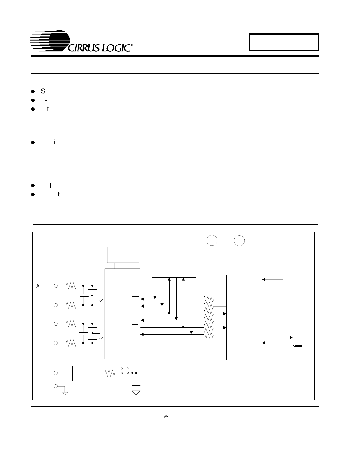
The CDB5550 is an excellent means for quickly evaluating the functionality and performance of the CS5550 A/D
converter. The CS5550 datasheet is supplied in conjunction with the CDB5550 evaluation board.
The evaluation board includes a C8051F320 microcontroller, a USB interface, drivers, and firmware. The
microcontroller controls the serial communication between the evaluation board and the PC via the firmware,
enabling quick and easy access to all of the CS5550’s
registers and functions.
The CDB5550 includes software for Data Capture, Time
Domain Analysis, Histogram Analysis, and Frequency
Domain Analysis.
ORDERING INFORMATION
CDB5550 Evaluation Board
AIN1+
AIN1+
AIN1-
AIN1-
AIN2+
AIN2+
AIN2-
AIN2-
Ext
Ref
Ext
Gnd
Ref
Gnd
Cirrus Logic, Inc.
http://www.cirrus.com
Sele ctable
Selectable
Divider
Divider
CRYSTAL
4.096 MHz
4.096 MHz
CS5550
AIN1+
AIN1+
AIN1-
AIN1-
AIN2+
AIN2+
AIN2-
AIN2-
OUT
CRYSTAL
CS5550
CS
SDI
SDO
SDO
SCLK
SCLK
RESET
INT
RESET
VREF
OUT
VREF
IN
Interface Header
Interface Header
CS
SDI
INT
IN
Copyright © Cirrus Logic, Inc. 2004
(All Rights Reserved)
+5 V
+5 V
GND
GND
C8051F320
C8051F320
Microcontroller
Microcontroller
RESET
CIRCUITRY
CONNECTOR
USB
CONNECTOR
RESET
CIRCUITRY
USB
JUN ‘04
DS630DB1
1
Page 2

TABLE OF CONTENTS
1. HARDWARE ............................................................................................................................. 4
1.1 Introduction ........................................................................................................................ 4
1.2 Evaluation Board Overview ................................................................................................ 4
1.2.1 Analog Section ...................................................................................................... 4
1.2.2 Digital Section .......................................................................................................5
1.3 Power Supply ..................................................................................................................... 6
2. SOFTWARE .............................................................................................................................. 6
2.1 Installation Procedure ........................................................................................................6
2.2 Using the Software ............................................................................................................. 6
2.2.1 Start-Up Window ................................................................................................... 6
2.2.2 Setup Window ....................................................................................................... 8
2.2.3 Calibration Window ............................................................................................... 9
2.2.4 Conversion Window .............................................................................................. 9
2.2.5 Data Collection Window ...................................................................................... 11
2.3 Retrieving Saved Data From a File .................................................................................. 13
2.4 Analyzing Data ................................................................................................................. 13
2.5 Histogram Information ......................................................................................................14
2.5.1 MEAN ............................................................................................................................14
2.5.2 STD_DEV .....................................................................................................................15
2.5.3 VARIANCE ....................................................................................................................15
2.5.4 MAXIMUM .....................................................................................................................15
2.5.5 MINIMUM ......................................................................................................................15
2.5.6 BIN .................................................................................................................................15
2.5.7 MAGNITUDE ................................................................................................................15
2.6 Frequency Domain Information ........................................................................................ 16
2.6.1 S/PN ..............................................................................................................................16
2.6.2 SINAD ...........................................................................................................................16
2.6.3 S/D .................................................................................................................................16
2.6.4 SNR ...............................................................................................................................16
2.6.5 FREQUENCY ...............................................................................................................16
2.6.6 MAGNITUDE ................................................................................................................16
2.6.7 # of AVG ........................................................................................................................16
2.7 Time Domain Information ................................................................................................. 17
2.7.1 MAXIMUM .....................................................................................................................17
2.7.2 MINIMUM ......................................................................................................................17
2.7.3 COUNT .........................................................................................................................17
2.7.4 MAGNITUDE ................................................................................................................17
3. REVISIONS ............................................................................................................................. 23
CDB5550
2
Page 3

LIST OF FIGURES
Figure 1. CDB5550 Start-Up Screen...............................................................................................6
Figure 2. CDB5550 Setup Options.................................................................................................. 7
Figure 3. CDB5550 Menu Options ..................................................................................................7
Figure 4. CDB5550 Setup Window ................................................................................................. 8
Figure 5. CDB5550 Calibration Window ......................................................................................... 9
Figure 6. CDB5550 Conversion Window ...................................................................................... 10
Figure 8. CDB5550 Configuration Window ................................................................................... 12
Figure 9. CDB5550 Histogram Plot............................................................................................... 14
Figure 10. CDB5550 Frequency Domain Plot ............................................................................... 16
Figure 11. CDB5550 Time Domain Plot........................................................................................ 17
Figure 12. Digital Section and Power Supply................................................................................ 18
Figure 13. Analog Section............................................................................................................. 19
Figure 14. Silkscreen .................................................................................................................... 20
Figure 15. Top Side....................................................................................................................... 21
Figure 16. Bottom Side ................................................................................................................. 22
LIST OF TABLES
Table 1. Analog Input Selection ...................................................................................................... 4
Table 2. VREFIN Source Selection................................................................................................. 5
Table 3. External Voltage Divider Selection.................................................................................... 5
Table 4. Revisions......................................................................................................................... 23
CDB5550
3
Page 4
CDB5550
1. HARDWARE
1.1 Introduction
The CDB5550 evaluation board provides a quick means of evaluating the CS5550 A/D converter. The
CDB5550 evaluation board’s analog section operates from a single +5 V power supply. The evaluation
board interfaces the CS5550 to an IBMTM compatible PC via a USB interface. To accomplish this, the
board comes equipped with a C8051F320 microcontroller and a USB connector which physically interfaces the evaluation board to the PC. Additionally, analysis software provides easy access to the internal
registers of the CS5550, and provides a means to display the performance in the time domain or frequency domain.
1.2 Evaluation Board Overview
The board is partitioned into two main sections: analog and digital. The analog section consists of the
CS5550, analog inputs, and an optional external voltage reference input. The digital section consists of
the microcontroller, interface header, reset circuitry, and the USB interface. The board also provides two
binding posts for easy power supply connectivity.
1.2.1 Analog Section
The CDB5550 provides several options for driving the analog inputs into the converter. These options include an external analog source, the voltage reference, and ground. Refer to Table 1.
Reference Description J11 Reference Description J5
AIN1+
VREF
GND
Selects the external
analog input (J13)
Selects the voltage ref-
erence sourced from
J7
Selects the ground
reference
O O AIN1+
O O VREF
O O GND
O O AIN1+
O O VREF
O O GND
O O AIN1+
O O VREF
O O GND
AIN2+
VREF
GND
Selects the external
analog input (J10)
Selects the voltage ref-
erence sourced from
J7
Selects the ground
reference
O O AIN2+
O O VREF
O O GND
O O AIN2+
O O VREF
O O GND
O O AIN2+
O O VREF
O O GND
Reference Description J14 Reference Description J9
AIN1-
VREF
GND
Selects the external
analog input (J13)
Selects the voltage ref-
erence sourced from
J7
Selects the ground
reference
O O AIN1O O VREF
O O GND
O O AIN1O O VREF
O O GND
O O AIN1O O VREF
O O GND
AIN2-
VREF
GND
Selects the external
analog input (J10)
Selects the voltage ref-
erence sourced from
J7
Selects the ground
reference
O O AIN2O O VREF
O O GND
O O AIN2O O VREF
O O GND
O O AIN2O O VREF
O O GND
Table 1. Analog Input Selection
The external analog inputs also provide +5 V and ground connectors which can be used to power a load
cell.
4
Page 5
CDB5550
The CDB5550 also provides options for sourcing the voltage reference for the CS5550. These options
include the on-chip reference (VREFOUT), or an external reference. The voltage reference selection is
controlled via the header J7. Refer to Table 2.
Reference Description J7
Ext VREF
CS5550 VREFOUT
Selects the external voltage reference
(J4)
Selects the internal voltage reference
from the CS5550
Table 2. VREFIN Source Selection
O O VREFOUT
O O Ext VREF
O O VREFOUT
O O Ext VREF
A selectable voltage divider for the external reference is also provided. The external voltage applied to the
terminal block J4 can be divided by a factor of 1, 2, 4, or 8. The voltage divider is controlled by header J1.
Refer to Table 3.
Reference Description J7
O O /1
O O /2
O O /4
O O /8
O O /1
O O /2
O O /4
O O /8
O O /1
O O /2
O O /4
O O /8
/1
/2
/4
Divides the external voltage applied to J4
by a factor of 1
Divides the external voltage applied to J4
by a factor of 2
Divides the external voltage applied to J4
by a factor of 4
O O /1
O O /2
O O /4
O O /8
/8
Divides the external voltage applied to J4
by a factor of 8
Table 3. External Voltage Divider Selection
1.2.2 Digital Section
The digital section of the CDB5550 consists of the microcontroller, interface header, reset circuitry, and
the USB interface. The microcontroller handles the communication between the PC and the CS5550. This
device is pre-programmed and requires no additional code in order to operate.
An SPI interface header is provided via J8 for use with an external microcontroller. However, if an external
microcontroller is used, the on-board microcontroller (U3) must be disconnected from the SPI port. This
can be accomplished by removing the 0 ohm resistors R11, R12, R13, R15, R17, and R18.
The CDB5550 has a pushbutton reset switch, S1. This reset button will reset the microcontroller which
will then reset the CS5550, resetting all registers to their default values.
5
Page 6
CDB5550
1.3 Power Supply
Power is supplied to the CDB5550 via two binding posts, +5 V (J2) and GND (J3). The +5 V supply powers
the analog core of the CS5550 and the internal regulator of the microcontroller. The microcontroller regulator outputs a +3.3 V supply which is used to power the microcontroller as well as various other logic
blocks.
The digital core of the CS5550 is powered from the regulated +3.3 V supply. However, the CDB5550 can
easily be modified to run the digital supply of the CS5550 at +5 V by removing R8 and populating R9 with
a 0 ohm resistor.
2. SOFTWARE
The evaluation board comes with software and a USB cable to link the evaluation board to the PC. The
software is designed to run under Windows 98TM or later. After installing the software, read the readme.txt
file for any last minute updates or changes.
2.1 Installation Procedure
The CDB5550 comes with an auto-booting CD that contains the required software to interface to the evaluation board. To install the software, place the CD into the CDROM drive and follow the on-screen instructions. The user will be prompted to select the destination for the installed program.
2.2 Using the Software
Before launching the software, the user should set up the CDB5550 evaluation board, select the proper
jumper settings as described in Section 1, and connect the board to an open USB port on the PC using
the provided cable. Once the board is powered on, the user can start the software program.
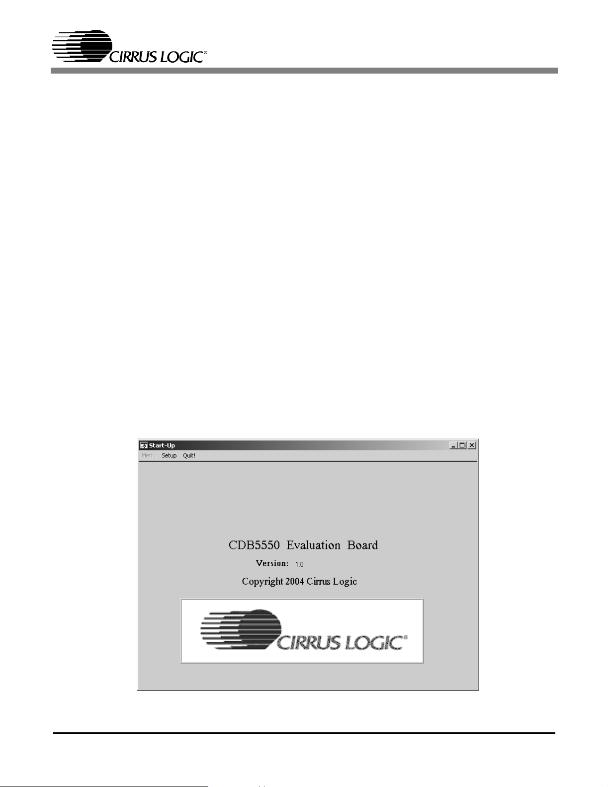
2.2.1 Start-Up Window
When the software is launched, the Start-Up window will appear. This window contains information concerning the software’s title, revision number, copyright date, etc. See Figure 1.
Figure 1. CDB5550 Start-Up Screen
6
Page 7
CDB5550
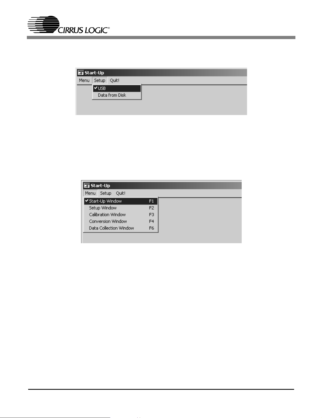
A pop-up window will also appear prompting the user to select the appropriate data source from the Setup
menu, located in the upper left hand corner of the Start-Up window. The user has two options: USB and
Data from Disk. See Figure 2.
Figure 2. CDB5550 Setup Options
If the USB setup is selected, the evaluation software will be ready to communicate with the CDB5550 via
the USB connection. If the Data from Disk setup is selected, the evaluation software will prompt the user
to select the appropriate data file. This option allows the user to view previously captured data without
having a CDB5550 connected to the PC. See Section 2.3 for more details.
After the user selects the appropriate setup, the Menu option becomes available in the Start-Up window.
The Menu pull-down has five options: Start-Up Window, Setup Window, Calibration Window, Conversion
Window, and Data Collection Window. See Figure 3.
Figure 3. CDB5550 Menu Options
7
Page 8

CDB5550
2.2.2 Setup Window
The Setup Window allows the user to access the internal registers of the CS5550. From this window the
user can click the View Register Values button to see the current values loaded in the Configuration,
Mask, Status, and Cycle Count Registers. The Status Register will default to 1h because the invalid command bit is active low. See Figure 4.
Figure 4. CDB5550 Setup Window
2.2.2.1. CS5550 Crystal Speed
The CS5550 accepts a wide range of crystal input frequencies, and can therefore run at many different
sample rates. The crystal frequency being used with the CS5550 should be entered in this box to provide
accurate frequency calculations in the FFT window. The CDB5550 comes with a 4.096 MHz crystal, which
is the default value in the Crystal Speed window.
2.2.2.2. Mask Register / Status Register
The Mask and Status Registers are displayed in hexadecimal and decoded in this box to indicate the function of each bit. The Mask Register can be modified by typing a value in the hexidecimal display box, or
by checking the appropriate check boxes for the bits that are to be masked. The Status Register cannot
be directly modified. It can only be reset by pressing the Clear Status Register button. The hexidecimal
display box for this register and the on-screen LEDs are read only. A LED that is on means that the corresponding bit in the Status Register is set (except the Invalid Command bit, which is inverted).
Note: The value present in the Mask register may be changed by the software during certain operations to provide
correct functionality of the CDB5550 board.
2.2.2.3. Reading the Board ID EPROM
The CDB5550 utilizes an on-board EPROM that contains the board identification. This can be useful if the
same board can be used with multiple devices. By clicking on the “Read EPROM” button in the lower left
corner, the character string stored in the EPROM will be temporarily displayed. For the CDB5550, this
string will read, “CDB5550A0”.
8
Page 9

CDB5550
2.2.3 Calibration Window
The Calibration Window allows the user to perform Offset and Gain calibrations on both channels. To perform an Offset calibration, connect the analog input to the referenced zero point (typically ground) and
click on the calibration (cal) button for that given channel. The resulting calibration value will be displayed
in both hexadecimal and decimal form below the button for that channel. To perform a Gain calibration,
apply a full-scale signal to the analog input and click on the calibration (cal) button for that given channel.
Please note that the input full-scale value will change based on the internal amplifier gain setting and reference voltage. Refer to the CS5550 datasheet for more information.
Figure 5. CDB5550 Calibration Window
2.2.3.1. View Cal Registers Button
The View Cal Registers button will display the calibration values stored in the CS5550 calibration registers. If the CS5550 has been previously calibrated and not powered down or reset, then the CS5550 calibration registers will contain the previous calibration values. The calibration registers must be cleared
prior to performing a calibration. To clear these registers, reset the CS5550 by pressing the board reset
switch, S1, or cycle the power.
2.2.4 Conversion Window
The user can perform conversions and display the results using the Conversion Window, see Figure 6.
The CS5550 provides both filtered and unfiltered conversion results for both channels. The unfiltered and
filtered data displays are updated at the end of each cycle count, which is determined by the cycle count
register. A cycle count of 4000 results in the data being updated once every second. A cycle count of 400
9
Page 10

CDB5550
will result in the data being updated ten times a second. Please note that the software only supports cycle
counts between 400 to 4000 when in the Conversion Window.
Figure 6. CDB5550 Conversion Window
2.2.4.1. Single Conversion Button
On pressing this button, a single conversion will be performed. After the conversion is complete, the Result data column will update with the values present in each data register.
2.2.4.2. Continuous Conversions Button
This button functions similarly to the Single Conversion button, except that continuous conversions are
performed instead. The data on the screen is updated in the same fashion, and the Stop button terminates
this action. The Mean and Standard Deviation columns will update every N cycles, where N is the number
in the Samples to Average box.
2.2.4.3. Standby/Sleep/Power Up Buttons
The Conversion Window also contains the power mode control for the CS5550. The user can select
among normal operation (Power Up), Standby Mode, or Sleep Mode. To exit Standby or Sleep mode, click
the Power Up button. Refer to the CS5550 datasheet for more information on the various power states.
10
Page 11

CDB5550
2.2.5 Data Collection Window
The Data Collection Window allows the user to collect sample sets of data from the CS5550 and analyze
them using time domain, FFT, and histogram plots. The user can then output this data to a file or make a
hardcopy of the display.
Figure 7. CDB5550 Data Collection Window
2.2.5.1. Time Domain / FFT / Histogram Selector
This menu selects the type of data processing to perform on the collected data and display in the plot area.
Refer to the section on Analyzing Data for more information.
11
Page 12

CDB5550
2.2.5.2. Config Button
This button will bring up the configuration window, in which the user can modify the data collection specifications. Refer to Figure 8.
Figure 8. CDB5550 Configuration Window
Number of Samples
This box allows the user to select the number of samples to collect, between 16 and 4096.
Average
When doing FFT processing, this box will determine the number of FFTs to average. FFTs will be collected and averaged when the Collect button is pressed.
FFT Window
This box allows the user to select the type of windowing algorithm for FFT processing. Windowing algorithms include the Blackman, Blackman-Harris, Hanning, 5-term Hodie, and 7-term Hodie. The 5-term
Hodie and 7-term Hodie are windowing algorithms developed at Cirrus Logic.
Histogram Bin Width
This box allows for a variable “bin width” when plotting histograms of the collected data. Each vertical bar
in the histogram plot will contain the number of output codes contained in this box. Increasing this number
may allow the user to view histograms with larger input ranges.
Input Channel Select
There are four check boxes on the right side of the Configuration window which allow the user to select
what data is displayed. The user has the option to select between channel 1 and channel 2, using either
the filtered or unfiltered conversion results.
2.2.5.3. Collect Button
This button will collect data from the part, to be analyzed in the plot area.
2.2.5.4. Output Button
This button will bring up a window in which the user can output the raw data to a file for later use, save
the FFT data, save the histogram data, print out a plot, or print out the entire screen.
12
Page 13

CDB5550
Note: When saving data, only the data channel being displayed on the plot will be saved to a file.
2.2.5.5. Zoom Button
This button allows the user to zoom in on the plot by selecting two points in the plot area. Press the Restore button to return to the normal data plot, or press the Zoom button again to zoom in even further.
2.3 Retrieving Saved Data From a File
The CDB5550 software allows the user to save data to a file, and retrieve it later when needed. To load
a previously saved file:
1) Pull down the Setup option and select Disk. A file menu will appear.
2) Find the data file and select it. Press the Select button to return.
3) Go to the Data Collection Window, and press the Collect button.
4) The data from the file should appear on the screen. To select a different file, repeat the procedure.
Note: Only time domain data can be loaded from a file. Data saved as FFT data or Histogram data cannot
be loaded. However, time domain data can be displayed as an FFT or histogram when reloaded.
2.4 Analyzing Data
The evaluation software provides three types of analysis tests - Time Domain, Frequency Domain, and
Histogram. The Time Domain analysis processes acquired conversions to produce a plot of Magnitude
versus Conversion Sample Number. The Frequency Domain analysis processes acquired conversions to
produce a magnitude versus frequency plot using the Fast-Fourier transform (results up to Fs/2 are calculated and plotted). Also, statistical noise calculations are calculated and displayed. The Histogram analysis test processes acquired conversions to produce a histogram plot. Statistical noise calculations are
also calculated and displayed.
13
Page 14

CDB5550
2.5 Histogram Information
The following is a description of the indicators associated with Histogram Analysis. Histograms can be plotted in the Data Collection Window by setting the Time Domain / FFT / Histogram selector to Histogram. Figure 9 shows a typical histogram plot.
Figure 9. CDB5550 Histogram Plot
2.5.1 MEAN
Indicator for the mean of the data sample set. The mean is calculated using the following formula:
n - 1
X
i
n
Mean =
Σ
i = 0
14
Page 15

CDB5550
2.5.2 STD_DEV
Indicator for the Standard Deviation of the collected data set. The Standard Deviation is calculated using
the following formula
n - 1
(Xi - Mean)
2
Σ
StDev =
2.5.3 VARIANCE
Indicates the Variance for the current data set. The variance is calculated using the following formula:
n - 1
i = 0
n
(Xi - Mean)
2
Σ
Var =
2.5.4 MAXIMUM
Indicator for the maximum value of the collected data set.
2.5.5 MINIMUM
Indicator for the minimum value of the collected data set.
2.5.6 BIN
Displays the x-axis value of the cursor on the Histogram.
i = 0
n
2.5.7 MAGNITUDE
Displays the y-axis value of the cursor on the Histogram.
15
Page 16

CDB5550
2.6 Frequency Domain Information
The following describes the indicators associated with FFT (Fast Fourier Transform) Analysis. FFT data
can be plotted in the Data Collection Window by setting the Time Domain / FFT / Histogram selector to FFT.
Figure 10 illustrates a typical Frequency Domain plot.
Figure 10. CDB5550 Frequency Domain Plot
2.6.1 S/PN
Indicator for the Signal-to-Peak Noise Ratio (decibels).
2.6.2 SINAD
Indicator for the Signal-to-Noise + Distortion Ratio (decibels).
2.6.3 S/D
Indicator for the Signal-to-Distortion Ratio, 4 harmonics are used in the calculations (decibels).
2.6.4 SNR
Indicator for the Signal-to-Noise Ratio, first 4 harmonics are not included (decibels).
2.6.5 FREQUENCY
Displays the x-axis value of the cursor on the FFT display.
2.6.6 MAGNITUDE
Displays the y-axis value of the cursor on the FFT display.
2.6.7 # of AVG
Displays the number of FFT’s averaged in the current display.
16
Page 17

CDB5550
2.7 Time Domain Information
The following controls and indicators are associated with Time Domain Analysis. Time domain data can
be plotted in the Data Collection Window by setting the Time Domain / FFT / Histogram selector to Time
Domain.
Figure 11. CDB5550 Time Domain Plot
2.7.1 MAXIMUM
Indicator for the maximum value of the collected data set.
2.7.2 MINIMUM
Indicator for the minimum value of the collected data set.
2.7.3 COUNT
Displays current x-position of the cursor on the time domain display.
2.7.4 MAGNITUDE
Displays current y-position of the cursor on the time domain display.
17
Page 18

CDB5550
18
Figure 12. Digital Section and Power Supply
Page 19

CDB5550
Figure 13. Analog Section
19
Page 20

CDB5550
Figure 14. Silkscreen
20
Page 21

CDB5550
Figure 15. Top Side
21
Page 22

CDB5550
Figure 16. Bottom Side
22
Page 23

3. REVISIONS
t
f
t
c
A
A
A
t
Table 4. Revisions
Revision Date Change
1 June 2004 Initial Release
CDB5550
Contacting Cirrus Logic Support
For a complete listing of Direct Sales, Distributor, and Sales Representative contacts, visit the Cirrus Logic web site at:
http://www.cirrus.com/corporate/contacts/sales.cfm
IMPORTANT NOTICE
Cirrus Logic, Inc. and its subsidiaries ("Cirrus") believe that the information contained in this document is accurate and reliable.
However, the information is subject to change without notice and is provided "AS IS" without warranty of any kind (express or
implied). Customers are advised to obtain the latest version of relevant information to verify, before placing orders, that
information being relied on is current and complete. All products are sold subject to the terms and conditions of sale supplied at
he time of order acknowledgment, including those pertaining to warranty, patent infringement, and limitation of liability. No
responsibility is assum ed by C irrus for the use of this information, including use of this information as the basis for m anufac ture or
sale of any items, or for infringement of patents or other rights of third parties. This document is the property of Cirrus and by
urnishing this information, Cirrus grants no license, express or implied under any patents, mask work rights, copyrights,
rademarks, trade secrets or other intellectual property rights. Cirrus owns the copyrights associated with the information
ontained herein and gives consent for copies to be made of the information only for use within your organization with respect to
Cirrus integrated circuits or other products of Cirrus. This consent does not extend to other copying such as copying for general
distribution, advertising or promotional purposes, or for creating any work for resale.
CERTAIN APPLICATIONS USING SEMICONDUCTOR PRODUCTS MAY INVOLVE POTENTIAL RISKS OF DEATH,
PERSONAL INJURY, OR SEVERE PROPERTY OR ENVIRONMENTAL DAMAGE (“CRITICAL APPLICATIONS”). CIRRUS
PRODUCTS ARE NOT DESIGNED, AUTHORIZED OR WARRANTED FOR USE IN AIRCRAFT SYSTEMS, MILITARY
PPLICATIONS, PRODUCTS SURGICALLY IMPLANTED INTO THE BODY, LIFE SUPPORT PRODUCTS OR OTHER
CRITICAL APPLICATIONS (INCLUDING MEDICAL DEVICES, AIRCRAFT SYSTEMS OR COMPONENTS AND PERSONAL OR
UTOMOTIVE SAFETY OR SECURITY DEVICES). INCLUSION OF CIRRUS PRODUCTS IN SUCH APPLICATIONS IS
UNDERSTOOD TO BE FULLY AT THE CUSTOMER’S RISK AND CIRRUS DISCLAIMS AND MAKES NO WARRANTY,
EXPRESS, STATUTORY OR IMPLIED, INCLUDING THE IMPLIED WARRANTIES OF MERCHANTABILITY AND FITNESS FOR
PARTICULAR PURPOSE, WITH REGARD TO ANY CIRRUS PRODUCT THAT IS USED IN SUCH A MANNER. IF THE
CUSTOMER OR CUSTOMER’S CUSTOMER USES OR PERMITS THE USE OF CIRRUS PRODUCTS IN CRITICAL
PPLICATIONS, CUSTOMER AGREES, BY SUCH USE, TO FULLY INDEMNIFY CIRRUS, ITS OFFICERS, DIRECTORS,
EMPLOYEES, DISTRIBUTORS AND OTHER AGENTS FROM ANY AND ALL LIABILITY, INCLUDING ATTORNEYS’ FEES AND
COSTS, THAT MAY RESULT FROM OR ARISE IN CONNECTION WITH THESE USES.
Cirrus Logic, Cirrus, and the Cirrus Logic logo designs are trademarks of Cirrus Logic, Inc. All other brand and product names in
his document may be trademarks or service marks of their respective owners.
23
 Loading...