

CS5542
CS5543
22-Bit, Multi-Channel
Features
l
Delta-Sigma Architecture:
- 5th Order Modulator
- 22-Bit Resolution
l
dc Accuracy (fBW = 250Hz):
- Integral Linearity: ±0.001 % F.S.
- Differential Linearity: ±0.5 LSBs
- RMS Noise: 1.1 pA
l
Pin Selectable Input Range:
- ±400 nA to ±2.5 µA Full Scale
l
8-Channel Digital FIR Filter
l
Self-calibration of Offset and Gain
l
Low Power: 50 mW /ch for 8-ch system
RMS
∆Σ
ADC Chip Set
Description
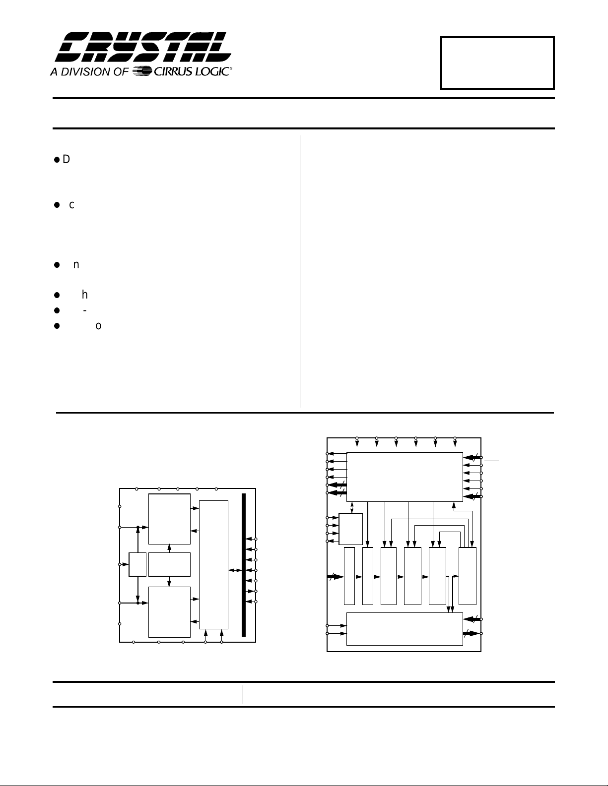
The CS5542 / CS5543 chip set is desi gned to be a complete current measurement data acquisition system.
The CS5542 is a 22-Bit, 2-channel, 5th-order delta sigma modulator. The CS5543 is a monolithic CMOS, 8channel digital FIR filter designed to be used with up to
four CS5542’s forming an 8-channel system. The complete system is capable of cascading up to 1024
channels.
The system supports 22-bit measurement resolution
with output conversion rates up to 1 kHz per channel.
JTAG boundary-scan capability is available to facilitate
self-test a t the system level.
Potential applications for the CS5542/CS5543 system
are environmental monitoring, process control systems,
color sensing, light measurement, chemical analyzers
and photo-diode transducer applications.
ORDERING INFORMATION
CS5542-KL 0 to 70°C 28-pin PLCC
CS5543-KL 0 to 70°C 28-pin PLCC
VA+ VA- GNDLVD+DGND
ICAL
MUX
5th Order
Delta-Sigma
Modulator
Left
Channel
Bias
Regulator
5th Order
Delta-Sigma
Modulator
Right
Channel
Calibra-
tion
and
Digital
Control
Logic
REFGNDL
INL
ICAL
INR
REFGNDR
VREF+ VREF- GNDR SEL0SEL1
Preliminary Product Information
Cirrus Logic, Inc.
Crystal Semiconductor Products Division
P.O. Box 17847, Austin, Texas 78760
(512) 445 7222 FAX: (512) 445 7581
http://www.crystal.com
VD1+GND1VD2+GND2VD3+GND3
CAPSIZE
PDN
MCLK
FSYNC
CAL[1:0]
MDATA[3:0]
C[2:0]
CAPSIZE
MCLK
FSYNC
PDN
C[2.0]
CAL[1:0]
TCK
TMS
TDI
TDO
MDATA
[3:0]
DAT ACLK
FRAME
3
Access
4
2
Test
Port
Fir Filter
Data Decode
Control/Sequencing
Calibration
System Offset
Noise Calibration
Serial I/O
System Or ITest
3
DMODE[2:0]
RST
CLKIN
FEGAIN
OE
DATSEL[3:0]
4
Registers
Offset/Gain
Gain Calibration
DATAIN[3:0]
4
DATAOUT
4
[3:0]
CS5543CS5542
This document contains information for a new product.
Cirrus Logic reserves the right to modify this product without notice.
Copyright Cirrus Logic, I nc. 1997
(All Rights Reserv ed)
DS109PP2
SEP ‘96
1
CS5542 CS5543
ANALOG CHARACTERISTICS: (T
& DGND= 0V;VREF+ = 4V, VREF- = -4 V; MCLK frequency as noted.)
Parameter Min Typ Max Units
Specified Temperature Range 0 - 70 °C
Accuracy
Full Scale Input Current (Bipolar)
CAPSIZE=0 (Note 1)
CAPSIZE=1 (Note 1)
Dynamic Range
CAPSIZE=0 (Note 1)
CAPSIZE=1 (Note 1)
Differential Nonlinearity (No Missing Codes) (Note 2) 22 - - Bits
Integral Nonlinearity (Note 1) - - 0.001 %FS
Full Scale Error (Note 3) - - 0.1 %FS
Full Scale Drift (Note 3) - 30 - ppm/°C
System Offset Calibratio n Range (Note 4) - - 10 %FS
Offset Drift (Note 1) - ±0.3 - LSB/°C
Power Supplies (Note 5)
Consumption
Active
Powerdown
50, 60 Hz Power Supply Rejection: VA+ or VA- (Notes 1, 6) - TBD - dB
Fullscale Current = 400 nA
60 Hz
500 Hz
Fullscale Current = 2500 nA
60 Hz
500 Hz
= 25° C; VA+, VD+ = 5 V ± 5%; VA- = -5 V ±5%; GNDL,GNDR,
A
-
-
106
113
-
-
-
-
-
-
400
2500
109
116
-
-
1.85
13.5
1.88
15.3
80
10
-
-
-
-
-
-
-
-
nA
nA
dB
dB
mW
mW
nA/V
nA/V
nA/V
nA/V
Notes: 1. Full scale current is tested under two conditions: CAPSIZE = 0 (CDAC = 1.6 pF) with MCLK at 1.024
MHz and CAPSIZE = 1 (CDAC = 4.8 pF) with MCLK at 2.048 MHz. Dynamic Range (Signal -to-No ise) i s
tested with 101 Hz si ne wave voltage dr iven into a 5 M
from INR or INL to REFGNDR or REFGNDL respectively, to test each modulator. S/N and integral
nonlinearity are tested with CAPSIZE = 0 (CDAC = 1.6 pF) with MCLK at 2.048 MHz and CAPSIZE = 1
(CDAC = 4.8 pF) with MCLK at 1.024 MHz.
2. Guaranteed by design or characterization.
3. Specificatio n applies after a complete calibrati on sequence using the CS5542/CS5543 combi nation. Drift
specification i s for the CS5542/CS554 3 only and does not include drift due to the input components, the
VREF voltage, or a frequency change of CLKIN.
4. Specification ap plies only to System Offse t Calibrat ion using the CS5542/ CS5543 chip combin ation aft er
Input Offset Voltage calibration has been completed with no external offset applied to the input.
5. The VA+ and VA- supplies should be quiet supplies (see data sheet text). Power supply sequence is
important. The VA+ and VA- supplies should be applied to the CS5542 prior to or at the same time as
the VD+ supply.
6. Power supply rejection is tested with a 100 mVp-p sine wave applied to each supply. See data sheet
text for power supply noise requirements.
2 DS109PP2
Ω input resisto r with a 470 pF capac itor connect ed
MCLK
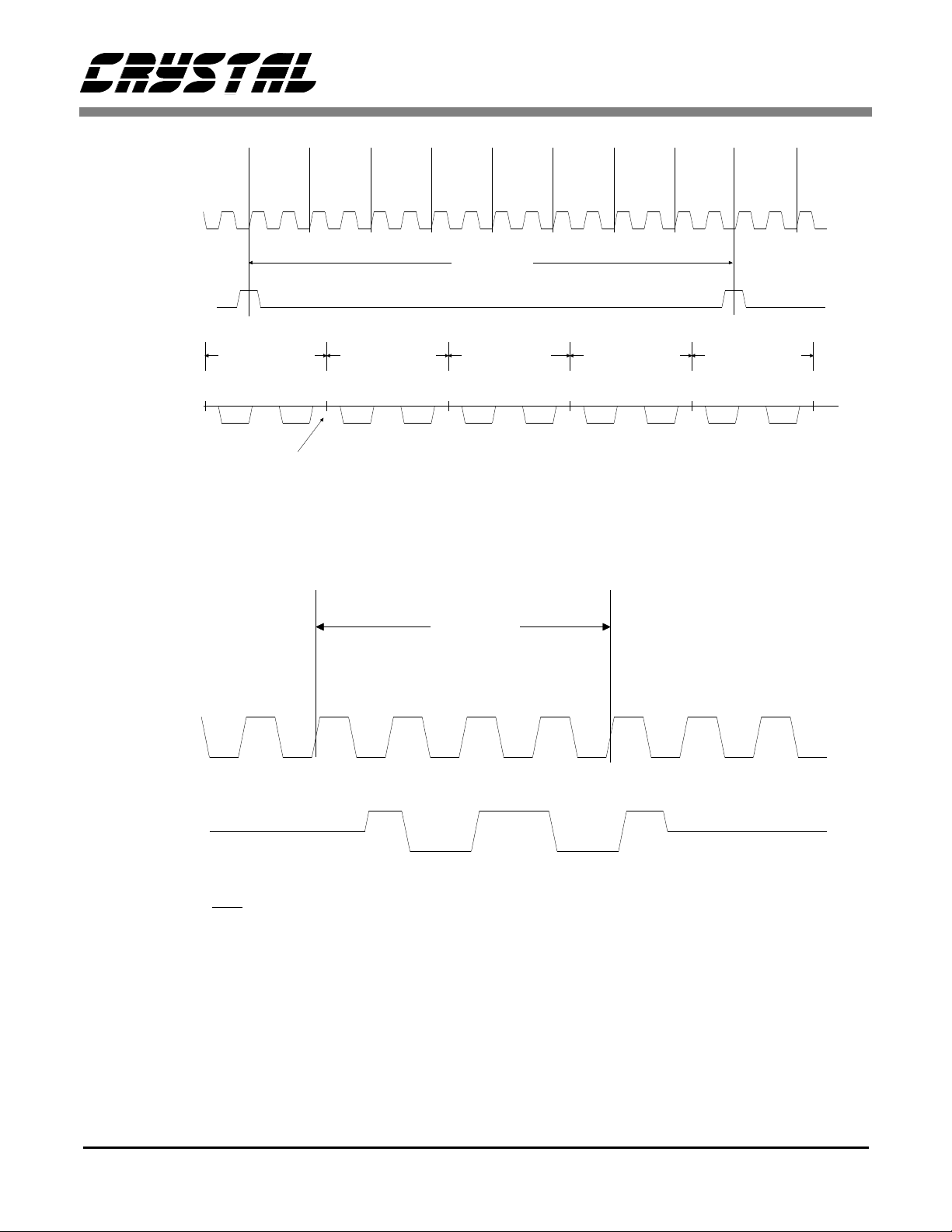
(2048 x OWR)
FSYNC
(Modulator
Fs Rate)
SLOT6 SLOT7 SLOT0 SLOT1 SLOT2 SLOT3 SLOT4 SLOT5 SLOT7SLOT6
(Previou s
Frame)
(Previous
Frame)
ONE FRAME
8 CHANNELS
4 SLOT-PAIRS
CS5542 CS5543
MDATA3:0
MCLK
CHIP #4 ACTIVE
(Previous Frame)
L
INTER-CHIP
HANDOFF POINT
CHIP #1 ACTIVE
SLOT PAIR #1
R
L
R
CHIP #2 AC TIVE
SLOT PAIR #2
L
CHIP #3 ACTIVE
SLOT PAIR #3
R
L
R
CHIP #4 ACTIVE
SLOT PAIR #4
L
R
CS5542 Frame Timing Overview
ONE SLOT
PAIR
MDATA[3:0]
LEFT
DATA
RIGHT
DATA
HI-Z STATE (Note 1)HI-Z STATE (Note 1)
Notes
1
Hi-Z State shown as intermediate level for clarity only.
Bus capacitance would n or mall y maintain valid logic one
level during Hi-Z until next time slot pair becomes active.
CS5542 MDATA3-MDATA0 Output Timing Characteristics
DS109PP2 3
CS5542 CS5543
CS5542 / CS5543 SYSTEM SWITCHING CHARACTERISTICS: (T
VD2+ = VD3+ = 5 V ±5%; GND1 = GND2 = GND3 = 0 V; For timing parameters: CLKIN= 2.048 MHz; DATACLK =
6.144 MHz; MCLK = 2.048 MHz; Outputs loaded with 50 pF.)
Parameter Number Min Typ Max Units
CS5542 Modulator Timing
MCLK Frequency 0 1.024 - 2.048 MHz
MCLK Duty Cycle 1 40 - 60 %
FSYNC Frequency 2 FSYNC set-up before MCLK rising edge 3 70 - - ns
FSYNC hold time after MCLK rising edge 4 70 - - ns
MCLK rising to MDATA[3:0] valid 5 70 ns
MCLK rising to MDATA[3:0] high 6 70 ns
MCLK falling to MDATA[3:0] to Hi-Z 7 70 ns
MCLK falling to MDATA[3:0] active 8 70 ns
CS5543 System Timing
CLKIN Frequency (1/Clock Period) 9 1.024 - 2.048 MHz
CLKIN Duty Cycle 10 40 - 60 %
DATACLK Frequency (1/Clock Period) 11 3.072 - 6.144 MHz
DATACLK Duty Cycle 12 40 - 60 %
FRAME rising to CLKIN rising 13 20 ns
FRAME rising to next DATACLK rising 14 20 ns
FRAME period 15 1 ms
CLKIN rising to MCLK rising 16 0 50 ns
CLKIN falling to MCLK falling 17 0 50 ns
CS5542 /CS5543 Interface
FSYNC period 18 - 7.81 - µs
MCLK falling to FSYNC rising or falling 19 0 70 ns
CS5543 to CS5543 Interface
DATACLK rising to DATAOUT valid 20 65 ns
DATAIN set-up time before DATACLK rising 21 0 15 ns
DATAIN hold time after DATACLK rising 22 15 15 ns
MCLK/
= 25°C, VD1+ =
A
16
-Hz
4 DS109PP2
DATACLK
TCK, CLKIN
FRAME
DATAIN [3:0]
DATAOUT [3:0]
DMODE [2:0],
DATSEL[3:0],
JTAG pins,
OE, FEGAIN
MCLK
FSYNC
CS5542 CS5543
11
13
14
20
21
22
16 17
19
3
19
4
18
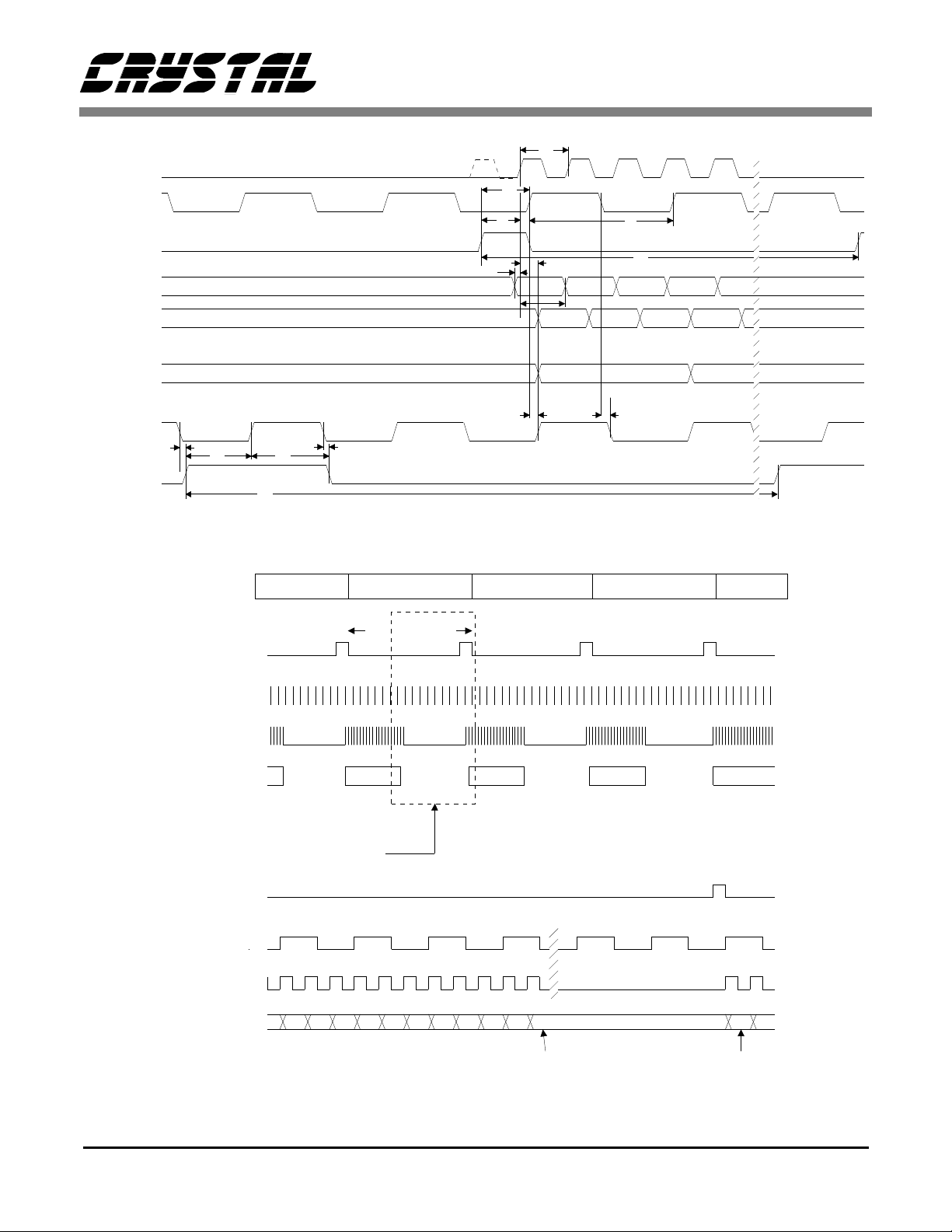
CS5542/CS5543 System Timing Diagram
9
15
valid data
valid data
Output Word Cycle N - 1 N N + 1 N + 2 N + 3
1 Filter Output Time
FRAME
CLKIN
DATACLK
DATAOUT [3:0]
N - 2N - 3
N - 1
N
Expanded inter-view timing
FRAME
CLKIN
DATACLK
DATAOUT [3:0]
parity bit from
"most remote" channel
(end of Frame N-3)
sign bit from
"nearest" channel
(beginning of Frame N-2)
Multi-Frame System Timing Diagram
DS109PP2 5
CS5542 CS5543
CS5543 FILTER CHARACTERISTICS: (T
GND2 = GND3 = 0 V; Output Word Rate (OWR) = CLKIN/2048)
Parameter Min Typ Max Units
Passband - - 0.5 OWR
-3 dB Frequency - 0.536 - OWR
Equivalent Noise Bandwidth 0.536 OWR
Stop Band 0.016 0.5
Stop Band Rejection (CS5543 only) 120 dB
Stop Band Rejection (CS5542/43 Combination) 127 dB
Group Delay 3/OWR s
Group Delay vs. Frequency (Linear Phase) 0 s
Decimation Ratio (CS5543 input to output) 128
= 25°C, VD1+ = VD2+ = VD3+ = 5 V ±5%; GND1 =
A
128 X
OWR
6 DS109PP2
CS5542 CS5543
0
-30
-60
-90
-120
-150
H(z), dB
-180
-210
-240
-270
-300
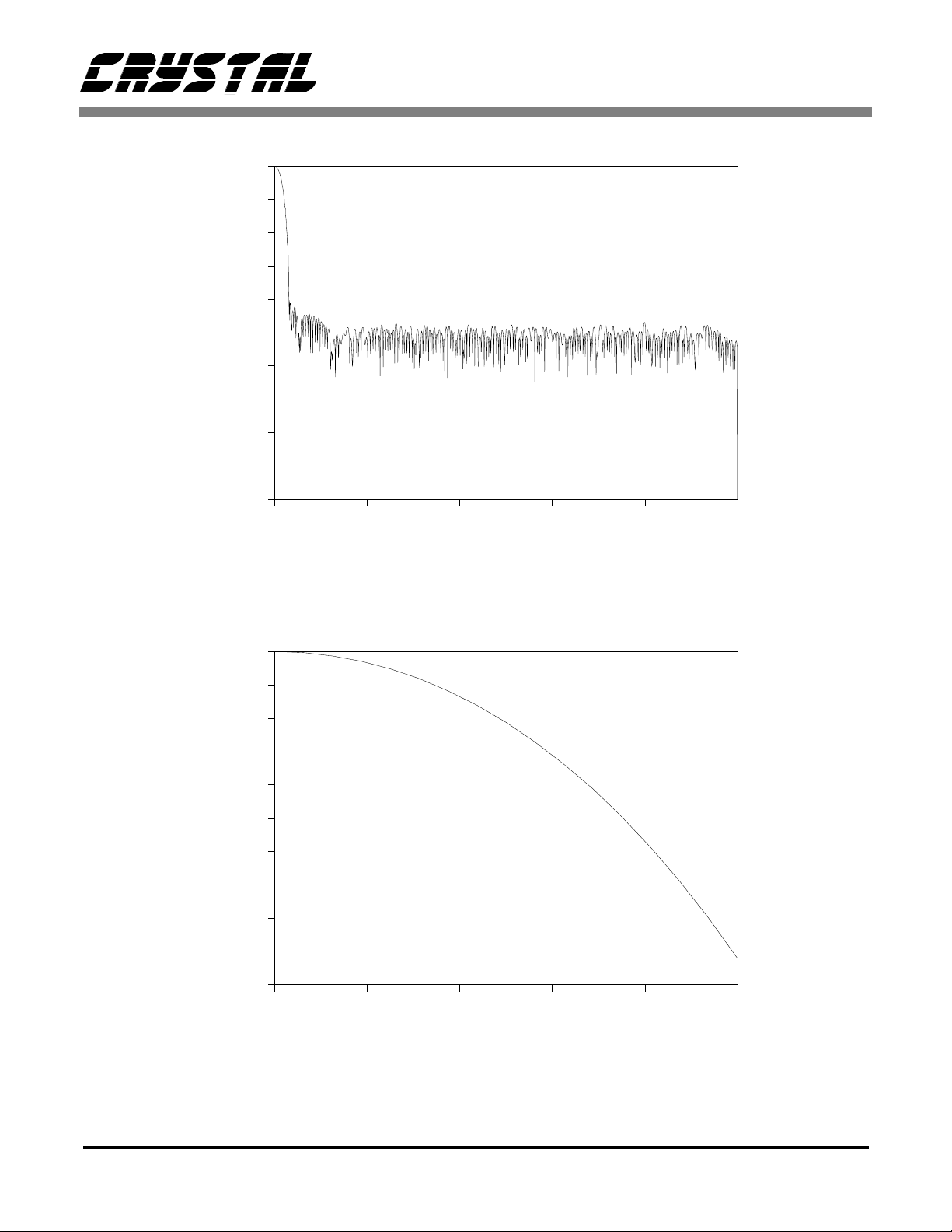
0.0 0.1 0.2 0.3 0.4 0.5
Normalized to Modulator Sample Frequency
Modulator Sample Frequency = MCLK/16; Output Word Rate = MCLK/2048 Hz
Digital Filter Total Response
-0.0
-0.3
-0.6
-0.9
-1.2
-1.5
H(z), dB
-1.8
-2.1
-2.4
-2.7
-3.0
0.0 0.1 0.2 0. 3 0.4 0.5
Normalized to Output Word Rate
CS5543 Digital Filter Passband Response
DS109PP2 7
CS5542 CS5543
CS5542 DIGITAL CHARACTERISTICS: (T
= 25°C, VD+ = 5 V ±5%; DGND = 0V; Output loaded
A
with 50 pF)
Parameter Symbol Min Typ Max Units
High-Level Input Voltage V
Low-Level Input Voltage V
High-Level Output Voltage (I
Low-Level Output Voltage (I
out = 600µA) Voh VD+ -0.4 - - V
out = 800µA) Vol --0.4V
Input Leakage Current (All pins except OE = Logic 0) I
Input Leakage Current (OE pin only, OE pin = Logic 0) I
Output Leakage Current
ih VD+ -1.0 - - V
il --1V
in --10µA
in --25µA
I
out
--10µA
Digital Input Capacitance Cin -7-pF
Digital Output Capacitance C
out -7-pF
CS5542 RECOMMENDED OPERATING CONDITIONS: (GNDR = GNDL = REFGNDR =
REFGNDL = DGND = 0V)
Operating Voltages
Positive Analog VA+ 4.75 5.0 +5.25 V
Negative Analog VA- -4.75 -5.0 -5.25 V
Positive Digital VD+ 4.75 5.0 +5.25 V
VREF+ VREF+ 2.0 4.0 4.1 V
VREF- VREF- -2.0 -4.0 -4.1 V
Parameter Symbol Min Typ Max Units
CS5542 ABSOLUTE MAXIMUM RATINGS*: (Voltages with respect to GND = 0V)
Parameter Symbol Min Typ Max Units
Source Transient Voltage into INL and INR inputs (Note 7) - - 1000 V
Source Transient Current into I NL and INR inputs - - 100 mA
Operating Voltages
Positive Analog
Negative Analog
Positive Digital
Input Current, Any Pin Except Supplies I
Digital Input Voltage V
Storage Temperature T
Notes: 7. Transient model is 100 pF through a 1500 ohm source resistance.
*Warning: Operation beyond these limits may result in permanent damage to the device
Normal operations not guaranteed at these extremes
VA+
VA-
VD+
in --±10mA
IND -0.3 - (VD+)+0.3 V
stg -65 150 °C
-0.3
+0.3
0.3
-
-
-
6.0
-6.0
(VA+)+0.3
V
V
V
8 DS109PP2
CS5542 CS5543
CS5543 POWER SUPPLY: (T
= 25°C; CLKIN = 2.048 MHz; DATACLK = 6.144 MHz, VD+ = 5.25 V;
A
GND1 = GND2 = GND3 = 0V)
Parameter Symbol Min Typ Max Units
Consumption
Active
Powerdown
CS5543 DIGITAL CHARACTERISTICS: (T
= 25°C, VD+ = 5 V ±5%; GND1 = GND2 = GND3 =
A
75
95
-
1700
mW
uW
0V; Output loaded with 50 pF)
Parameter Symbol Min Typ Max Units
High-Level Input Vol tage V
Low-Level Input Voltage V
High-Level Output Voltage (I
Low-Level Output Voltage (I
out = -600µA) Voh VD+-0.4 - - V
out = 800µA) Vol --0.4V
Input Leakage Current I
Output Leakage Current
ih VD+-1.0 - - V
il --1V
in --10µA
I
out
--10µA
Digital Input Capacitance Cin -7-pF
Digital Output Capacitance C
out -7-pF
CS5543 RECOMMENDED OPERATING CONDITIONS: (GND1 = GND2 = GND3 = 0V, All
voltages with respect to 0V.)
Parameter Symbol Min Typ Max Units
Digital DC Supply VD+ 4.75 5.0 5.25 V
Supply Voltage Required to Maintain Ca li bration Information 4.0 - - V
CS5543 ABSOLUTE MAXIMUM RATINGS*: (GND = 0V, All voltages with respect to 0V.)
Parameter Symbol Min Typ Max Units
Power Supplies: VD1+
VD2+
VD3+
Input Current (Except Supply Pins)
Digital Input Voltage
I
in
V
inp
Storage Temperature Tstg -65 150 °C
*Warning: Operation beyond these limits may result in permanent damage to the device
Normal operations not guaranteed at these extremes
-0.3 6.0 V
±10.0 mA
-0.3 (VD+)+0.3 V
DS109PP2 9

CS5542 CS5543
GENERAL DESCRIPTION
The CS5542 is a monolithic CMOS dual delta-sigma modulato r. Each modul a tor in t he CS55 42 a ccepts a low level current input, usually supplied by
a photodio de (see Figure 1). This current is digitized by the CS 5542 mo dulator and filter ed by the
CS5543 digital FIR decimation filter. Four CS5542
modulator chips can be combined with one CS5543
filter chip to provide eight channels of data conversion as shown in Figure 2. Up to 128 8-channel
blocks of CS5542/CS5543 chip sets can be connected to build a 1024 channel system as shown in
Figure 3. T he CS5542/CS554 3 combination sup ports several c alibratio n mod es for the data a cquisition system.
Differential
Voltage
Reference
THEORY OF OPERATION
The CS5542/ CS5543 chip set is designe d to construct multi-channel current input digitizer systems. The conversion clock input (CLKIN) into
the CS5543 provides the master cloc k for the digi tal filter. T his cloc k can be as fast as 2.048 MH z.
CLKIN is buffered inside the CS5543 and is passed
to each of the CS5542 modulator chips as the
MCLK (modulator clock) signal. The CS5542/
CS5543 combination provides output conversion
data at a word rate equal to CLKIN/20 48.
Reference
-4.0 V
Note 2
Note 1
Note 1
+4.0 V
.1µF
5
INL
Photodiode
6
REFGNDL
4
GNDL
8 MEG
Note 1: Diodes can be connected with either polarity. As shown the CS5542/43 will
generate a more negative code as the photodiode outputs more current.
2: The ICAL current can be of either polarity. Its magnitude will determine the
full scale measurement range.
FS
I
R
I
Photodiode
10 µF
10
ICAL
8
INR
7
REFGNDR
9
GNDR
.1µF
VREF+
13
-4.0 V
.1µF
32 14
VREF- SEL0
CS5542
MDATA [3:0]
VA-
-5V
VA+ VD+ DGND
12
+5 V
.1µF10
10
µ
F
23
Ω
.1µF
15
SEL1
CAPSIZE
PDN
MCLK
FSYNC
CAL [1:0]
C [2:0]
22
1
11
17
16
19, 18
28,27,26
25,24,21,20
AGND
DGND
To
CS5543
2
3
4
Decimator
Figure 1. CS5542 Typical Connection Diagram
10 DS109PP2

CS5542 CS5543
INL0
INR0
ICAL
INL1
INR1
INL2
INR2
INL3
INR3
INL
INR
ICAL
INL
INR
ICAL
INL
INR
ICAL
INL
INR
ICAL
MDATA[3:0]
CS5542
MDATA[3:0]
CS5542
MDATA[3:0]
CS5542
MDATA[3:0]
CS5542
C[2:0]
CAL[1:0]
FSYNC
MCLK
PDN
CAPSIZE
SEL1
SEL0
C[2:0]
CAL[1:0]
FSYNC
MCLK
PDN
CAPSIZE
SEL1
SEL0
C[2:0]
CAL[1:0]
FSYNC
MCLK
PDN
CAPSIZE
SEL1
SEL0
C[2:0]
CAL[1:0]
FSYNC
MCLK
PDN
CAPSIZE
SEL1
SEL0
DGND
DGND
DGND
VD+
VD+
DGND
VD+
VD+
CAPS
PDN
MCLK
FSYNC
CAL[1:0]
C[2:0]
MDATA[3:0]
CS5543
DATAOUT[3:0]
FRAME
DATCLK
CLKIN
DATAIN[3:0]
DATSEL[3:0]
DMODE[2:0]
RST
TCK
TMS
TDI
TDO
OEOE
FEGAINFEGAIN
FRAME
DATCLK
CLKIN
DATAOUT [3:0]
DATAIN[3:0]
DATSEL[3:0]
DMODE[2:0]
RST
TCK
TMS
TDI
TDO
Supplies omitted for cl ar i ty
Figure 2. Typical 8-channel Connection Diagram
DS109PP2 11

CS5542 CS5543
m
Current Inputs
IN0
IN1
IN2
IN3
IN4
IN5
IN6
IN7
ICAL0
IN8
IN9
IN10
IN11
IN12
IN13
IN14
IN15
ICAL1
INL0
INR0
INL1
INR1
INL2
INR2
INL3
INR3
ICAL
8-channel Block 0
INL0
INR0
INL1
INR1
INL2
INR2
INL3
INR3
ICAL
8-channel Block 1
TDI
DATAIN[3:0]
OE
FEGAIN
RST
TCK
TMS
FRAME
DATACLK
CLKIN
DATSEL[3:0]
DMODE[2:0]
DATAOUT[3:0]
TDO
TDI
DATAIN[3:0]
OE
FEGAIN
RST
TCK
TMS
FRAME
DATACLK
CLKIN
DATSEL[3:0]
DMODE[2:0]
DATAOUT[3:0]
TDO
From TDO of previous I E EE 1149.1 - compliant device in s yste
DATAIN[3:0]
OE
FEGAIN
RST*
TCK
TMS
FRAME
DATACLK
CLKIN
DATSEL[3:0]
DMODE[2:0]
Host
System
Interface
IN1016
IN1017
IN1018
IN1019
IN1020
IN1021
IN1022
IN1023
ICAL127
INL0
INR0
INL1
INR1
INL2
INR2
INL3
INR3
ICAL
DATAIN[3:0]
OE
FEGAIN
RST
TCK
TMS
FRAME
DATACLK
CLKIN
DATSEL[3:0]
DMODE[2:0]
TDI
8-channel Block 127
Figure 3. Typical 1024 Connection Diagram
12 DS109PP2
DATAOUT[3:0]
TDO
To TDI of next IEEE 1149.1 - compliant device in system
DATAOUT[3:0]

CS5542 CS5543
The CS5542 i ncludes two modul ators. The input
current into each of the modulators is set by the following factor s: the MCLK (mo dulator clock) frequency, the value of the VREF voltage to
modulator chip, and the logic value of the CAPSIZE input t o the CS5542 mod ulator (this select s
either a 1.6 pF or a 4.8 pF transimpedance feedback
capacitor). MCLK is typically set as some frequency between 1.024 MHz and 2.048 MHz. The
VREF voltage is optimally set to 4.0 Volts. The
voltage refe ren ce fo r the mo dulat or is ac tuall y in put into bot h the VR EF+ an d VREF- pins as +4 .0
and -4.0 volts.
The full s cale input cu rrent is defined by th e following equation:
(V
REF
) X (C
) X (MCLK/16) = I
DAC
FS
With VREF = 4.0, MCLK = 2.048 MHz, and
CDAC se t to sele ct 1.6 pF , the nom inal ful l scale
current will be set at 819 nA. The value of the offset and gain reg ister c onten ts will affect the actu al
conversion words whi ch are output from the con verter with a specific input current. Several calibration steps (to be discusse d later) are necessary to
ensure tha t the chip converts accurately .
22 data bits (21 bits plus sign).
There are several clocks which control t he timing
to the multi-channel system. CLKIN (Master
Clock) is the prim a ry clock to the system. CLKIN
(typically 2.048 MHz) is input to the CS5543 filter.
Inside the fil ter CLKIN is buffere d and passed to
the CS5542s as MCLK. For each two clock cycles
of MCLK to the modulator, a four bit modulator
sample is passed t o the CS 5543 digi tal fil ter. The
digital filte r computes an out put conversion word
for each se t of 1024 modul ator sam ples. The o utput word rate of the filter is therefore related to the
CLKIN or MCLK frequency by the ratio
CLKIN/2048 = OWR (output word rate). The conversion data for ei ght CS5542 m odulato r chann els
is output from the four CS5543 DATAOUT pins in
a serial-formatted, time-multiplexed fashion. The
DATACLK controls the rate at which data is output
from the DATAOUT pins. DATACLK is three
times the frequenc y of CLKIN.
The CS5542/CS 5543 chip set is designed to support construct ing a serially-c onnected curre nt digitization system with up to 1024 channels.
System Initialization and Calibration
The CS5542 dual modulator and CS5543 multichannel filter are designed to interface together.
The CS554 2 modula tor us es a tr i-leve l mod ulator.
The modulator thresholds must be calibrated before
accurate measurem ents ca n be accomplished. The
threshold values are measured and digitally corrected inside the CS5543 digital filter. The
CS5543 digital fi lter func tions as a digita l calib ration engin e and a comm unic ations interf ace in addition to being a n FIR fi lter.
The CS5543 digital filter collects the multi-bit
quantized d ata from f our du al m o dulat or C S554 2s
and computes offset and gain corrections to the data, yielding a 24-bit output word. The 24-bit output
data word includes an overflow bit, a parity bit, and
DS109PP2 13
After power is applied to the CS5542/CS5543 system, a reset must be issued to the CS5543 device by
taking the RST
pin low. This resets the gain register to 0.8 (199998(H)) and all other registers to 0.0.
After RST
is returned high , the rel ease of the RST
state is no t recognized until th e next rising edge of
the FRAME signa l.
After a reset is recognized, the CS5542/CS5543
system must complete a full set of calibration
steps before being used for measurement. Calibrations are performed by contro lling the states
of the DTEST (Digital Test Mode Select) pins
with the DATSEL (Data Select Mode) pins held
as logic 0s. Tables 1 and 2 illustrate the commands available via the DTEST and DATSEL

DATSEL[3:0] DTEST[2:0] FUNCTION
CS5542 CS5543
0 0 0 0
0 0 0 0
0 0 0 0
0 0 0 0
0 0 0 0
0 0 0 0
0 0 0 0
0 0 0 0
DTEST[2:0] DATSEL[3:0] FUNCTION DATA TYPE
0 0 0
0 0 0
0 0 0
0 0 0
0 0 0
0 0 0
0 0 0
0 0 0
0 0 0
0 0 0
0 0 0
0 0 0
0 0 0
0 0 0
0 0 1
0 1 0
0 1 1
1 0 0
1 0 1
1 1 0
1 1 1
0 0 0 0
0 0 0 1
0 0 1 0
0 0 1 1
0 1 0 0
0 1 0 1
0 1 1 0
0 1 1 1
1 0 0 0
1 0 0 1
1 0 1 0
1 0 1 1
1 1 X X
Normal Operation
Input Offset Voltage Cal
Noise Cal
System Offset Cal
Full-Scale Gain Cal (Uses ICAL input)
Full-Scale Gain Cal (Uses INL(INR) input)
Decimator and Modulator Power-Down
Modular Power Down
Table 1. Operation Modes
Normal Operation
Tri-State Dataout [3:0] Pins
Test Pattern #1
Test Pattern #2
Offset Cal Register Load
Offset Cal Register Load
Gain Cal Register Load
Noise Cal Register Load
Offset Cal Register Read
Offset Cal Register Read
Gain Cal Register Read
Noise Cal Register Read
Reserved
(SIGN, MSB first)
(- - -)
(MSW) (Note 1)
(LSW) (Note 2)
(MSW)
(LSW)
Notes: 1. MSW = Most Significant Word
2. LSW = Least Significant Word
Table 2. Control Modes
pins.
When entering calibration commands via the
DTEST lin es, the calibrati on steps must foll ow a
specific seque nce for the CS5542/CS55 43 pair to
be properly calibrated. Fig ure 4 illustrates the calibration sequence for the CS5542/CS5543 chip set.
After the RST
is issued, the chip set will be in the
normal mode. The first calibration step is the Input
System
Reset
Note: Main Current Input must be idle for all calibration modes except for Gain Cal using INL(INR).
Normal
Input Offset
Voltage
Cal
Figure 4. Calibration Sequence CS5542/CS5543
Offset Voltage Cal mode.
The CS5542 i s designed to digitiz e an input cur-
rent. This current is normally sou r ce d from a photodiode at t he input of the c hip. The Input Offset
Voltage Cal step is intended to remove any offset at
the front end of the modulator. This should be calibrated with no photodiode c urrent present . If the
phototdiod e is repl aced wit h a resisto r, the vol tage
Noise
Cal
System
Offset
Cal
INR(INL)
or ICAL
Gain Cal
Normal
14 DS109PP2

CS5542 CS5543
Noise Calibration Register
MSB
22
2232
R0 0 0 0
212
System Offset Registers
Upper 20 Bits
212
Lower 22 Bits
212
MSW
LSW
Sign
2232
0
23222
2
Sign Sign
22
21220
2
21220
2
Gain Registers
DecimalInteger
221
2
Reset to Binary 000.11001100110011001000 or 199998(H)
Note 1: All Parity bits are odd.
020
2
-12-2
2
Table 3. Calibration Registers
2
LSB
Parity
(Note 1)
LSB
Parity
(Note 1)
LSB
Parity
(Note 1)
LSB
Parity
(Note 1)
-19
LSB
0
0
0
should be zeroed before calibrating the Input Offset
Voltage Cal step. The Input Offset Voltage Cal
mode will re quire 23 filt er cycles (a filter c ycle is
one output conversion word) to complete. The
CS5543 will not accept new mode commands until
the 23 filter cycles have been completed, even if the
DTEST pin s are chang ed. After the 23 fil ter cycles, the calibration step is complete. Note that
when the Input Offset Voltage Cal command is initiated inside the CS5543 decimator, the modulators
of all of the CS5542 chips connected to the CS5543
will exec ute the ca libratio n step at th e same ti me.
There is no calibration word or register inside the
CS5543 which contains the calibration data for this
calibration step.
The next ca libration to b e performed is t he Noise
Cal. This cali bration step is ne cessary to calibra te
the quanti zer threshold of the mod u la tors. This ensures linearity in the multi-bit quantizer. The Noise
Cal lasts 409 filter cycles. Upon entering the Noise
Cal mode, the system offset registers are set to 0; all
gain registe rs are unaffected . The Noise Cal step
can be performed at any time and it can be performed indepe ndent of the other c alibration ste ps.
When this step is executed, all eight modulators associated w ith a CS 5543 ca l ibrat e at the sam e tim e.
At the end of the Noise Cal step, a 24-bit calibration
word is placed into the Noise Cal register inside the
CS5543.
After the modu lators have been calib rated by the
Noise Cal step, the System Offset Cal step is performed. The current present at the INL (INR) input
at the time the System Offset Cal is performed will
treated as the zero point of the converter transfer
function. The System Offset Cal step lasts 1028 filter cycl es. At t he en d o f the Sys tem O ffset Cal, a
signed 43-bit result is placed into two System Offset Cal registers (MSW and LSW; Most Significant
Word and Least Significant Word) inside the
CS5543. After the System Offset Cal is complete,
the next c alibration st ep is a gain ca libration. To
perform a gain cal ibrat ion, an input signal mu st be
DS109PP2 15

CS5542 CS5543
provided into the CS5542. The CS5542 dual modulator is designed to allow for two possible means
of inputting the signal necessary to perform this
calibration step. The input method chosen will dictate whether an ICAL Full-Scale Gain Cal or a System Full-Scale Gain Cal is to be performed.
At the input of the CS5542 is an ICAL pin. A current can be sour ced into thi s pin to provid e a calibration cu rrent to set th e full sca le point (ac tually
97% of the full scale value as will be discussed later) of the system . The current int o the ICAL pin
will be us ed to calibra te the ga in if the Ful l-Scale
Gain Cal mode (usi ng the ICAL in put) i s selec ted.
Note that the ICAL pin on the CS5542 is shared between the two modulators. Each modulator will be
calibrated sequ enti ally (onl y on e of e ight chan nel s
will be acti ve at a time duri ng the calibr at ion if the
ICAL Full- Scale Gain C al mode is exec uted. T he
CS5543 will sequ entia lly cali brate eac h o ne of t he
eight modulators associated with it. Each Gain Cal
requires 5 filter cycles; therefore 40 filter cycles
will elapse for the ICAL Full-Scale Gain C al. At
the end of the Gain Cal, a 24-bit calibration word is
placed into the Gai n Register of the CS5 543.
Selection of the ICAL Full-Scale Gain Cal mode
enables the ICAL input switch (note that the normal
current input remains active and its current will be
summed with the ICAL current when using this
mode). During an ICAL Full-Scale Gain Cal cycle,
only one ICAL input is active at any one time,
therefore a single external resistor and a voltage
source can supply a current which can be used to
calibrate all ei ght c h annels associated w ith a single
CS5543. Alternatively, four individual resistors
can be supplied, one for each CS5542 dual channel
ICAL input.
The magnit ude of the cali bration current should be
3% less than the desired full sca le curren t. Reca ll
that the nominal ful l s cale input current magnitude
is set by the size of the internal transimpedance ca-
pacitor, the clock rate, and the VREF voltage. The
output code pr oduced by this current will be 2
16
-1 or approximately 97% of full scale. The
2
21
97% gain po int can be c alibrated with currents as
low as 40% below th e nomina l full sc ale valu e set
by the clock rate, cap size, and VREF voltage. It is
preferable t o keep t he input current for cal ibration
within 20% of th e nomina l full scal e value as lower
levels of input calibr ation magn i tude will e xhi bit a
slight reduction in dynamic range.
If the Full-Scale Gain Cal mode using INL (INR) is
selected, the ICAL input MUX at the front of each
CS5542 is not used. Instead, the gain i s calibrated
using the curr en t inp ut in to the INL and INR pi ns.
Again, the current supplied should be 3% less than
the desired full scale value. The output code due to
21
this current wil l be set to 2
- 216 -1 or approxi-
mately 97% of full scale.
For either gain calibration mode (ICAL or INL
(INR)) the magnitude of the input current should be
97% of the nominal full scale, but the polarity is not
important. The current can be sink ed or sourced.
In either case the CS5543 will calibrate the positive
full scale point . Once ca librate d, curre nts into t he
INL or INR pins will result in a positive output
code, while currents out of the pins will yield a negative output code.
Calibration Reg iste r Readability
The CS5543 has registers which hold the digital
calibration words for each of the eight channels.
For each of the ch anne ls, the re a re four 24- bit registers. The Noise Cal and Gain Cal functions each
result in a 24-b it digi tal c alibratio n w ord, whe reas
the System Offset Cal function produces a 48-bit
calibration word which is split into two 24-bit registers. These registers can be read and their contents
stored into some nonvolatile storage from which
they can be recalled and reloaded if so desired.
The 48-bit Offset register contents must be read or
-
16 DS109PP2

channel 0 channel 4
CS5542 CS5543
DATAOUT [0]
channel 1 channel 5
DATAOUT [1]
channel 2 channel 6
DATAOUT [2]
channel 3 channel 7
DATAOUT [3]
LSB
OD
LSB
OD
LSB
OD
LSB
OD
Figure 5. Data Transfer Timing
written wi th two read c ycles using dif ferent com mands to rea d either the MSW (Mos t Significant
Word) or the LSW (L ea st Significant Word).
When reading or writing to the calibration registers, the regi ster contents are time-division mu ltiplexed into or out of the CS5543 in the same
manner as conversion data as shown in Figure 5.
ParityMSBSIGN
ParityMSBSIGN SIGN ParityMSB
ParityMSBSIGN SIGN ParityMSB
ParityMSBSIGN SIGN ParityMSB
SIGN ParityMSB
LSB
LSB
LSB
LSB
Test Pattern #1:
(all channels)
HEX BINARY
Test Pattern #1: (All channels)
A00001 0001 0000 0000 0000 0000 0001
Sign, MSB LSB, parity
OD
OD
OD
OD
In addition to writing or reading the calibration registers, the CS5543 provides several test modes.
Some of these test modes are as follows: The
DATAOUT [3:0] pins can be set to a high impedance output state; or either of two different test patterns can be requested to be output on the
DATAOUT [3:0] pins of the CS5543. See Table 4
for the test pattern information.
Commands to change c al ib ration mode s or control
modes should not be issued to the system while a
calibration is in progress. New data for the calibration or control modes is latched on every falling
edge of CLKIN and t akes effect on the follow ing
Channel HEX BINARY
0
1
2
3
4
5
6
7
Test Pattern #2:
(Unique for each c hannel)
1000A0
000A01
20A000
0A0001
450000
005001
800500
000051
0001 0000 0000 0000 0000 0001
0000 0000 0000 1010 0000 0001
0010 0000 1010 0000 0000 0000
0000 1010 0000 0000 0000 0001
0100 0101 0000 0000 0000 0000
0000 0000 0101 0000 0000 0001
1000 0000 0000 0101 0000 0000
0000 0000 0000 0000 0101 0001
Sign, MSB LSB, parity
Table 4. Test Patter ns
rising edge of FRAME.
DS109PP2 17

CS5542 CS5543
y
Sign
MSB LSB OD Parit
22
2232
Bipolar Input Current Output Code (Sign and 21 Data Bits)
Positi ve F ull Scale
Zero Input 0 0 0000 0000 0000 0000 0000
Negative Full Scale 1 1 1111 1111 1111 1111 1111
Note 1 Positive Full Scale is current going into the modulator.
D
= 2,097,151 [(IIN - IOF)/(IFS - IOF)] where D
OUT
current going into t he modulator during System Off set Voltage Calibrati on; I
is always positive in magnitude and will be the absolute value of the current going into either INL/INR or ICAL
pin, divided by 0.97; and I
1
21220
2
Figure 6. Data Conversion Word Format
1 0 0000 0000 0000 0000 0000
is the digital output code f rom the CS5543; IOF is the
OUT
FS
is the current going into the modulator during the conversion. 2,097,151 is 221 - 1.
IN
Table 5. Output Coding for CS5542/CS5543.
2
212
2
is the full sca le input current which
0
Conversion Coding
Each of th e channel s of the CS5543 output s a 24bit conversion data word. The word includes a sign
bit along with 21 additional data bits, an Oscillation
Detect flag (OD), and an odd parity bit. The format
of the data conversion word is shown in F igu re 6.
The OD bit is set whenever the modulator in the
CS5542 is overranged to the point of making it lose
stability. Under th is condition the outpu t data can
be erroneous. Th e OD bit can be set when ever t he
input magnitude exceeds the full scale point by
greater than 5%. The O D bit will be c leared whenever the modulator input comes back into proper
range.
Table 5 illustrates the output coding for the
CS5542/CS5543 chi p set. Positive current means
that current is flowi ng into the INL (INR) pin and
produces a positive output code .
pins. DATAOUT[0] outputs data from channe ls 0
and 4; DATAOUT[1] outputs data from channels 1
and 5; DATAOUT[2] outputs data from channels 2
and 6; and DATAOUT[3] outputs data from ch annels 3 and 7. Information from DATAOUT[0] is
output beginning with the sign bit of channel 0 and
ends with the p arity (odd) bit of c hannel 4. Data
out of the other DATAOUT pins follows the same
conventio n.
In a system, mult iple CS 5543s are c onnect ed with
the DATA OUT pins of on e CS5543 con nected to
the DATAIN pins of the next CS5543.
DATAOUT[3:0] lines will change immediately after the rising edge of DATA CLK, and be latched
into the DATAIN[3:0] pins on the next rising edge
of DATACLK.
A timing diagram whi ch shows eight channels of
data transfer from one CS5543 to another is shown
in Figure 5.
CS5543 Serial Data Interfac e
The serial data interface on the CS5543 has four input signals and four output signals. Data read from
the CS5543 is output from the DATAOUT[3:0]
18 DS109PP2
The data which is transmitted either to or from the
series-connected CS5543s is synchro nized by the
FRAME signal. FRAME should be a pu lse, one
CLKIN cycle wide, generat ed by falling edges of

>9V
10µF
10
CS5542 CS5543
+
LT1019-
5
1K
4.02K
Figure 7. Noise-Filtered Bandgap Reference
1K
10K
+
+
100µF
100µF
>9V
0.01µF
OP27
47K
1K
22
15µF+0.1µF
+
+4.0
CLKIN. FRAME will be la tched i nto the CS5 543
by the rising edge of CLKIN. This will subsequently generate an FSYNC signal to synchronize
the CS5542 mod ul at ors.
System Connections
An eight channel digitizer system can be constructed using four CS5542 dual modulators with one
CS5543 eight-channel decimator. Figure 2 illustrates the ha rdware signal conn ec tion s for a n ei ght
channel system .
Digitizer blocks of eight channels each can be cascaded to con nec t 128 bl ocks t ogeth er for a tot al o f
1024 digitiz er chann els. Al l clock s in the system
are related to the CL KIN master clock. Assuming
that CLKIN= 2.048 MHz, the converter output
word rate will be CLKIN/2048. A data framing
signal, FRAME, synchronizes the digital output
data and t he modulato r data. Th e FRAME signal
must occur at the output word rate. Th e DATACLK must be three times faster than the CLKIN
rate, 6.144 MH z i n thi s example.
The CS5543 has four DATAOUT lines. Each of
the lines prov ides an o ut put for the dat a fro m two
of the eight channels associated with a single
CS5543. Data from any one DATAOUT line is serially transferred out of the DATAOUT pin in 48bit blocks, consis ti ng of t w o 24-bit words.
With 128 CS5543 link e d together, each of th e four
serial lines linking DATAOUT pins to DATAIN
pins is in effect a serial shift register 6 144 (48 X
128) bits long. The DATACLK is used to shift data
out of each CS5543 in 48 bit blocks. For a 1024
channel system with an CLKIN rate of 2.048 MHz,
the 6.144 MH z DATACLK w ill shift out the data
for all 1024 channel s in one mill ise c ond.
Analog Input
The CS5542 modulator is op timized to be driven
by a photodiode current source. Photodiodes have
large output impedance s. A photod iode also ha s a
capacitance which is a function of its size. The
CS5542 relies on this capacitance to ensure the stability of it s input stage. The capacitance al so affects th e bandwidt h of the input cir cuit.
In all cases the modulator assumes that the external
shunt capacitance of the photodiode is at least
220pF.
If the input sou rce i s act uall y a vo ltag e so urce and
a resistor is used to generate the input current, a 220
pF capacitor sho uld be conn ected between the input pin and ground. The resistor will add additional
current noi se into the circui t and will degrade t he
dynamic range so m ewh at .
Voltage Reference
The volta ges supplied to the VREF+ and VR EF-
pins can rang e from ±2.0 volts to ±4.1 volts with
±4. 0 volts being preferred. VREF+ and VREFvoltages should be balanced and have low noise.
Figure 7 illustrates how a bandgap voltage reference can be well filtered to provide a low noise
source for +4.0 volts.
DS109PP2 19

CS5542 CS5543
Each VREF+ or VREF- input on a CS5542 may require up to 1 microamp of re ference current. The
number of channels which can be supplied from
one voltage ref erence buffe r will depend upon the
buffer’s output impedance and the distance between the CS5542 an d the reference circuitry . A
well-design ed voltage refere nce should be able to
supply 32 channe ls (16 CS5542s) in a syste m .
Board Layout
The circuit board containing the CS5542 modulator
should have a ground plane split through middle of
the modulato r with pins 2 thro ugh 13 over a q uiet
analog gro und plane. In ad dition, guardin g techniques should b e used around t he low level inputs
INL, INR, and ICAL. Care must also be exercised
to ensure that the circuit card is manufactured with
good quality to ensure lo w leakage. After assembly, the card sh ould be cleane d to ensure it is fr ee
from all surface contaminants.
Clock Source
CLKIN must have low jitter; less than 20 psec
RMS. Note that any drift in CLKIN ov er time or
temperature will show up as a gain error in the
CS5542/CS5543 measu rement system; th erefo re a
stable clock source is highly desirable.
Power Supply
Power supply noise and ripple must be very low
within the passband of the CS5543 digital filter.
This noise and ripple can pass through the ESD
(Electrostatic Discharge) protection diodes at the
INL (INR) pin into the transimpedance stage of the
CS5542 modul ator. With the capacita nce of this
diode at ab out 5 pF, a nd the tr ansim peda nce r esistor of the firs t stage at about 2 -10 megohm, co upling of sup ply ripple is g oing to occur. For this
reason, the n oise a nd rippl e on th e powe r supplie s
should be lo w enough that t he noise coupled into
the transimpedance stage should remain below the
noise floor of the converter across the bandwidth of
the digital filter. To achieve this, 60 Hz related
noise and ripple should remain below 50 microvolts peak-to-pe ak.
Digital Fi lter
The digita l filter is a linea r phase FIR filte r. The
filter has a group d elay of three conversion wor ds
and an equival ent noise bandwidth of 0.5 36 of the
output word frequency. Plots for the filter are
shown in the dat a shee t tables . Coef ficien ts are ta bulated in the Appendix of this data sheet.
Joint Test Action Group (JTAG)
Boundary-Scan Interface
The CS5543 is designed for large multi-channel
systems. For this reason the chip is designed to support the IEEE Standard Access Port and BoundaryScan Architecture as defined in IEEE Std. 1149.11990, or P1149.1. This standard defines circuitry
which is built into the an integrated circuit to assist
in the test, maintenance, and support of a system at
the printed circuit board level. The CS5543 includes circuitry which supports this standard.
It is highly recommended that if this type of test capability is desired in your syste m, th at you ac quire
a copy of the IEEE standard which thoroughly discusses the IEEE Sta ndard Ac cess Port a nd Bound ary-Scan Architecture as it will only be discussed
briefly here.
The CS5543 includes a TAP (Test Access Port)
made of the following connections: TCK (Test
Clock), TMS (Test Mod e Select input ), TDI (Test
Data Input), a nd T DO (T est Dat a Out put). In ad dition to the TAP, the test logic includes a TAP
controller, a n instruction registe r, and a set of test
registers. The TAP controll er is a synchronou s finite sta te mach ine wh ich co ntrols the seque nce o f
operations necessary to implement the boundaryscan architecture. Figure 8 illustrates the TAP controller state diagram. The instruction register allows an instruction to be shifted into the design.
20 DS109PP2

CS5542 CS5543
1
0
Test-Logic-Reset
0
Run-Test/Idle
1
Select-DR-Scan
1
0
Capture-DR
Pause-DR
Update-DR
Figure 8. TPA Controller State Diagram
The instru ctio n regist er is use d to sele ct th e test to
be performed or to select the test data register to be
accessed. The 3-bit instructions available in the instruction register are illustrated in Table 6. The
LSB of the 3-bit inst ruc tion is shifted in first.
IR CODE INSTRUCTION
000
001
010
011
100
101
110
111
Table 6. Boundary Scan Instructions
EXTEST
SAMPLE/PRELOAD
IDCODE
OPERATING MODE REGISTER
reserved
reserved
reserved
BYPASS
0
0
Shift-DR
1
Exit1-DR
0
1
Exit2-DR
1
1
1
0 0
Select-IR-Scan
1
Capture-IR
0
0
0
Shift-IR
1
Exit1-IR
0
Pause-IR
1
Exit2-IR
1
Update-IR
1
1
0101
of board interconnects. The bit ordering for the
BSR is the s ame a s the top -view p ackag ed pinou t,
clockwise beginning with the MDATA[3], and
ending with RST
. The TAP, power and gnd pins
are not included as part of the boundary-scan register. The BSR is 47 bits long. Inputs can be set via
the BSR, bypassing th e actual pin . All outputs are
3-state (logic high, low and or high impedance)
outputs. The ir stat es duri ng test can be contr olled
via the PRELOAD instruction. In the bound aryscan register, ea ch inp ut pin of t he devi ce is re presented by one bit position of the boundary scan register, whereas each of the outputs, having the
possibility of any one of three states, require two
bits each in the boundary-scan regi st er.
00
The Devic e Identifi cation Register is de signed to
Several test registers are in the design including the
Boundary-Scan Register (BSR), the Device Identification Registe r (DIR), the Operating Mode Register (OMR), and the Bypass Register (BR).
identify the manufacturer, the part number, and the
version numbe r of t he C S554 3. T he f orma t of t he
DIR is illust rated in Table 7. Data fro m the DIR is
shifted out of the TDO LSB first. Note that when
the CS5543 is rese t, the Instru ction Regi ster is set
The Boundar y-Scan Register al lows for the testing
DS109PP2 21
to select IDCODE.

CS5542 CS5543
The Operating Mode Register (OMR) allo ws access to the device operating modes via the DATASEL and DMODE pins as shown in figure 9.
The Bypass Register allows a minimum length path
between th e TDI and TDO pins on the de vice. This
register can be selected whenever the device does
not need to be tested during board-level te st operation.
DATSEL DMODE
TDI
OMR Bit #
Figure 9. Operating Mode Register
3 2 1 0 2 1 0
6 5 4 3 2 1 0
TDO
Device Identification Register
TAP Operation for EXTEST
Before execut ion of the instructio n EXTEST, the
SAMPLE/PRELOAD instruction must be used to
load testing data to all output pins through TDI.
Each outp ut pin requ ires two b its. The first b it to
be shifted in controls the output enable function. If
a logic 1 is entered, the output is enabled; if a logic
0 is entered, the out put is disabled. The second bit
shifted in af ter the first bit is the test da ta. Therefore, two TCK cy cles are required to load testing
data into the boundary-scan register for each output
pin.
MSB
31 16
V3 V2 V1 V0 P15 P14 P13 P12 P11 P10 P9 P8 P7 P6 P5 P4
LSB
15
P3P2P1P0M10M9M8M7M6M5M4M3M2M1M0 1
BIT NAME VALUE FUNCTION
V3-V0 Version Bits 0000 Version Number of Device
P15-P0 Part Number Bits 0101010101000011 Part Number of Device
M10-M0 Manufacture Number Bits 00001100100 Manufacture Number
L0 Logic 1 1 Always Logic 1
Table 7. Device Identification Register
0
22 DS109PP2

CS5542 PIN DESCRIPTIONS
CAPSIZE
CS5542 CS5543
Power Supplies
VREF-
VREF+
GNDL
INL
REFGNDL
REFGNDR
INR
GNDR
ICAL
PDN
VA+
VA-
SEL0
32724
5
6
7
8
9
10
11
12 14 16 1813 15 17
1
CS5542
TOP
VIEW
C2
C1
C0
MDAT A3
2628
25
24
23
22
21
20
19
MDAT A2
VD+
DGND
MDAT A1
MDAT A0
CAL1
CAL0
MCLK
FSYNC
SEL1
GNDL - Ground Left, Pin 4.
Left modula tor analog g round for inte grators 2 throu gh 5.
REFGNDL - Reference Ground Left, Pin 6.
Analog ground for left modula tor integra tor 1 and sum ming node.
GNDR - Ground Right, Pin 9.
Right modula tor analog g round for in tegrators 2 t hrough 5.
REFGNDR - Reference Ground Right, Pin 7
Analog ground for right mod ulator integr ator 1 and summing node.
VA+ - Positive Analog Supply, Pin 12.
Positive analo g supply volta ge. Nominal ly +5 volts.
VA- - Negative Analog Supply, Pin 13.
Negative analo g supply voltage . Nominally - 5 volts.
VD+ - Digital Supply, Pin 23.
Digital supply voltage. Nominally +5 volts.
DS109PP2 23

CS5542 PIN DESCRIPTIONS
DGND - Digital Ground, Pin 22.
Digital ground.
Digital Input Pins-
MCLK - Modulator Clock Input, Pin 17.
The modulato r clock input provide s the necessary clock for ope ration of the modula tor. MCLK
operates at 16 t imes the mod ulator samp le rate. M CLK is 2048 ti mes the out put word rate .
FSYNC - Frame Sync, Pin 16.
The transition from a low to high level on this input supplied by the CS5543, will reset the
internal ma ster timin g of the CS5542 and synchroni ze its data with each outp ut word.
CAL[1:0] - Calibration Co ntrol, Pins 19, 18.
The mode of operation for the CS5542 is selected through the calibration control pins via the
CS5543 and is summ arized in the table below.
CAL1 CAL0 Mode Selected
CS5542 CS5543
0 0 Normal Operation, Nois e CAL , Offset CAL
0 1 Input offset voltage calibrate
1 0 Unused code
1 1 Full Scale gain calibrate
Normal Calibrat ion Sequence
01 Input Offset
00 Noise CAL(Dark)
00 Offset CAL(Dark)
11 Gain CAL
00 Normal Operation
SEL[1:0] - Time Slot Se lection s, Pins 15,14
The binary code applied to SEL0 and SEL1 will determine the time slot pair associated with
the CS5542. E ach of th e up to four CS5542’s conne cted to a si ngle CS5543 must have a unique
code assig ned to th e combi nation of S EL0 an d SEL1.
CAPSIZE - Full Scale Input Range Select, Pin 1.
When CAPSIZE = 0, C
24 DS109PP2
= 1.6 pF; when CAPSIZE = 1, C
DAC
DAC
= 4.8 pF

CS5542 PIN DESCRIPTIONS
PDN - Power Down, Pin 11.
When asserted the CS5542 will e nter the power- down state.
C[2:0] - ICAL Input Select, Pins 28, 27, 26.
In an array of 4 CS5542’s (eight channels), C2-C0 will select which channel is to receive the
d.c. current applied to the ICAL p ins.
Digital Outputs Pins-
MDATA[3:0] - Modulator Data Outputs, Pins 25, 24, 21, 20.
The tri-level modulat or data is output on MDATA3 - MDATA0 for decimation by the CS5543.
Modulator Output Coding Table
Overload -1 zero +1
MDATA3 MDATA2 MDATA_1 MDATA0 Value / Meaning
CS5542 CS5543
1 0 0 1 +1 / Normal operation
1 0 1 0 0 / Normal operation
1 1 0 0 -1 / Normal op e r at ion
0 1 1 0 +1 / Modulator Overload
0 1 0 1 0 / Modulator Overloa d
0 0 1 1 -1 / Modulator Overload
As shown in the table above, a const ant number of zeros and ones exist for all out put states.
This provides a data-independent noise invariant coding to maximize isolation between channels.
Analog Input Pins -
VREF-,VREF+ - Differential Voltage Reference Inputs, Pins 2, 3.
A differential vol tage reference on t hese pins operate s as the voltage r eference for the CS 5542.
Nominally, it is -4.0 V and + 4.0 respectively.
ICAL - Full-Scale Current Calibration Input, Pin 10.
ICAL needs to be supplied f or full-scale ga in calibra tion.
INL, INR - Input Left and Input Right, Pins 5, 8.
INL and INR are t he left and r ight modul ator current in put pins.
DS109PP2 25

CS5543 PIN DESCRIPTIONS
DATAIN[0]
CS5542 CS5543
DATAIN[1]
DATAIN[2]
DATAIN[3]
C0
C1
C2
CAL[0]
CAL[1]
FSYNC
MCLK
GND1
VD1+
CAPS
PDN
MDATA[0]
MDATA[1]
MDATA[2]
7
8
9
10
11
12
13
14
15
16
17 29
46
18 20 22
12
CS5543
TOP
VIEW
44
24
4042
26 28
DATAOUT[0]
DATAOUT[1]
DATAOUT[2]
DATAOUT[3]
GND3
VD3+
DATACLK
39
38
37
36
35
34
33
32
31
30
FRAME
CLKIN
DATSEL[0]
DATSEL[1]
DATSEL[2]
DATSEL[3]
DTEST[0]
DTEST[1]
DTEST[2]
FEGAIN
MDATA[3]
TMS
TDI
TDO
OE
RST
VD2+
GND2
TCK
Power Supply
VD1+, VD2+, VD3+ - Digital Power Supplies, Pins 13, 25, 39.
Digital supply voltages. Nominally +5 Volts.
GND1, GND2, GND3 - Digital Ground, Pins 12, 24, 40.
Digital grounds.
DSM-DSD Interface Pins
C[2:0] - ICAL Channel Select (Outputs), Pin s 7, 6, 5.
In an array of 4 CS5542’s (eight channels), C2-C0 will select which channel is to receive the
d.c. current applied to the ICAL p ins during f ull-scale gai n calibrat ion.
26 DS109PP2

CS5543 PIN DESCRIPTIONS
CAL[1:0] - Calibration Co ntrol (Outputs), Pins 8, 9.
The mode of operation for the CS55 42 is selected through the calibratio n Control pins. See th e
table in the p in-out section of the CS55 42 data sheet fo r details.
FSYNC - Frame Sync (Output), Pin 10.
The transition from a low to high level at the CS5542’s input will reset the internal master
timing of the CS5542 and sync hronize it s data with eac h output wo rd from the C S5543.
MCLK - Modulator Cloc k (Output), Pin 11.
The modulat or clock out put provides the necessary cl ock for opera tion of the m odulator.
CAPSIZE - Full Scale Input Range Select (Output), Pin 14.
Controls the CAPSIZE input to the CS5542. This determines the size of the sampling capacitor
used by the CS5542.
PDN - Power Down (Output), Pin 15.
When asserted the CS5542 will e nter the power- down state.
CS5542 CS5543
MDATA[3:0] - Modulator Dat a Inputs (Inputs), Pins 16, 17, 18, 19.
The tri-level modulator data is input to the CS5543 via MDATA3 - MDATA0 for decimation.
See the table in the pi n-out secti on of the C S5542 data she et for deta ils.
Test Access Port Pins
TMS -Test Mode Select (Input), Pin 20.
Controls the state-to-s tate oper ation of the TAP con troller.
TDI - Test Data Input (Input) , Pin 21.
Serially inputs da ta to the Test Access Port.
TDO - Test Data Output (O utput), Pin 22.
Serially outputs data from the Test Access Port.
TCK - Test Clock (Input), Pin 23.
The clock for the Test Access Po rt, shorted to MC LK
Control Pins
OE - Output Enable (Input), Pin 27.
Enables or disab les (tri-stat es) all outp ut pins on t he CS5543.
FEGAIN - Front-End Gain Select (Input), Pin 28.
Selects the Front-End Capacitor Gain Ratio. A full calibration is necessary following any
change to this input.
DS109PP2 27

CS5543 PIN DESCRIPTIONS
DMODE[2:0] - Digi tal Mode Select (Inp uts), Pins 29, 30, 31.
Selects the op eration mo de of the CS55 43.
DATSEL[3:0] - Data Selection M ode (Inputs), Pins 32, 33, 34, 35.
Selects t he Data to be p laced on the DA TAOUT[3 :0] pins .
RST
- Chip Reset (Input), Pin 26
Resets all int ernal logi c and registers.
DSD-System Interface Pins
DATACLK - Serial Data Clock (Input), Pin 38.
Clock signal generated by the system controller which governs all serial output data timing
from the CS5543.
CLKIN - Master System Clock (Input), Pin 36.
A CMOS comp atible cloc k input to th is pin governs a ll non-seria l data timi ng.
CS5542 CS5543
FRAME - Framing Signal (Input), Pin 37.
Synchronizes DAT ACLK and MCLK for each frame of output da ta from the CS55 43.
DATAOUT[3:0] - Serial Output Data (Outputs), Pi ns 41-44.
CS5543 serial out put data.
DATAIN[3:0] - Serial Data Inputs (Inputs), Pins 1-4.
CS5543 serial input data from the serial output of the adjacent CS5543 in a multi-decimator
system.
28 DS109PP2

CS5542 CS5543
Filter Coefficients
h(0)=h(383)= -6 h(32 )=h( 351)= -298 8 h(64)=h(319)= -323 37 h(96)=h (287)= -66 63 h(128)=h(255)= 613898 h(160)= h(223)= 2 079544
h(1)=h(382)= -7 h(33 )=h( 350)= -332 7 h(65)=h(318)= -337 41 h(97)=h (286)= -22 9 h(129)=h(254)= 6 4963 7 h(161)=h(22 2)= 21268 69
h(2)=h(381)= -10 h(34 )=h( 349)= -369 5 h(66)=h(317)= -351 34 h(98)=h (285) = 6812 h(130)=h(253)= 6 86379 h(162)= h(221)= 2 1735 44
h(3)=h(380)= -15 h(35 )=h( 348)= -409 4 h(67)=h(316)= -365 08 h(99)=h (284) = 14489 h(131)= h(252 )= 72410 7 h(163)=h(22 0)= 2 219496
h(4)=h(379)= -21 h(36 )=h(347)= -452 4 h(68)=h(315)= -378 56 h(100)=h(283 )= 22 828 h(132)=h(251)= 7 6280 0 h(164)=h(21 9)= 22646 53
h(5)=h(378)= -29 h(37 )=h(346)= -498 8 h(69)=h(314)= -391 67 h(101)=h(282 )= 31 855 h(133)=h(250)= 8 0243 6 h(165)=h(21 8)= 23089 43
h(6)=h(377)= -39 h(38 )=h(345)= -548 7 h(70)=h(313)= -404 31 h(102)=h(281 )= 41 596 h(134)=h(249)= 8 4299 0 h(166)=h(21 7)= 23522 95
h(7)=h(376)= -52 h(39 )=h(344)= -602 1 h(71)=h(312)= -416 38 h(103)=h(280 )= 52 077 h(135)=h(248)= 8 8443 4 h(167)=h(21 6)= 23946 40
h(8)=h(375)= -67 h(40 )=h(343)= -659 4 h(72)=h(311)= -427 77 h(104)=h(279 )= 63 323 h(136)=h(247)= 9 2673 7 h(168)=h(21 5)= 24359 08
h(9)=h(374)= -85 h(41 )=h(342)= -720 5 h(73)=h(310)= -438 34 h(105)=h(278 )= 75 361 h(137)=h(246)= 9 6986 7 h(169)=h(21 4)= 24760 30
h(10)=h(373)= -107 h(42)=h(341)= -7856 h(74)=h (309)= -447 98 h(106)= h(277)= 88 214 h(138)=h(245 )= 10137 88 h(170)=h(213)= 2 514942
h(11)=h(372)= -133 h(43)=h(340)= -8549 h(75)=h(308)= -45655 h(10 7)=h(276 )= 10190 6 h(139)=h(244)= 1058463 h(171)=h(212)= 2552576
h(12)=h(371)= -163 h(44)=h(339)= -9283 h(76)=h(307)= -46389 h(10 8)=h(275 )= 11646 1 h(140)=h(243)= 1103850 h(172)=h(211)= 2588870
h(13)=h(370)= -199 h(45)=h(338)= -10060 h(77 )=h(306)= -46987 h(10 9)=h(274 )= 13190 0 h(141)=h(242)= 1149907 h(173)=h(210)= 2623763
h(14)=h(369)= -240 h(46)=h(337)= -10881 h(78 )=h(305)= -47431 h(11 0)=h(273 )= 14824 6 h(142)=h(241)= 1196589 h(174)=h(209)= 2657194
h(15)=h(368)= -287 h(47)=h(336)= -11745 h(79 )=h(304)= -47706 h(11 1)=h(272 )= 16551 8 h(143)=h(240)= 1243847 h(175)=h(208)= 2689106
h(16)=h(367)= -342 h(48)=h(335)= -12654 h(80 )=h(303)= -47793 h(11 2)=h(271 )= 18373 6 h(144)=h(239)= 1291632 h(176)=h(207)= 2719443
h(17)=h(366)= -404 h(49)=h(334)= -13608 h(81 )=h(302)= -47674 h(11 3)=h(270 )= 20291 8 h(145)=h(238)= 1339892 h(177)=h(206)= 2748154
h(18)=h(365)= -475 h(50)=h(333)= -14605 h(82 )=h(301)= -47330 h(11 4)=h(269 )= 22308 1 h(146)=h(237)= 1388572 h(178)=h(205)= 2775188
h(19)=h(364)= -556 h(51)=h(332)= -15646 h(83 )=h(300)= -46742 h(11 5)=h(268 )= 24424 0 h(147)=h(236)= 1437615 h(179)=h(204)= 2800497
h(20)=h(363)= -647 h(52)=h(331)= -16730 h(84 )=h(299)= -45888 h(11 6)=h(267 )= 26641 0 h(148)=h(235)= 1486965 h(180)=h(203)= 2824037
h(21)=h(362)= -750 h(53)=h(330)= -17856 h(85 )=h(298)= -44749 h(11 7)=h(266 )= 28960 2 h(149)=h(234)= 1536559 h(181)=h(202)= 2845767
h(22)=h(361)= -865 h(54)=h(329)= -19023 h(86 )=h(297)= -43301 h(11 8)=h(265 )= 31382 7 h(150)=h(233)= 1586337 h(182)=h(201)= 2865647
h(23)=h(360)= -995 h(55)=h(328)= -20228 h(87 )=h(296)= -41523 h(11 9)=h(264 )= 33909 4 h(151)=h(232)= 1636234 h(183)=h(200)= 2883642
h(24)=h(359)= -1139 h(56)=h(327)= -214 71 h(88)=h(295)= -393 91 h(120)=h(263 )= 36541 0 h(152)=h(231)= 1686186 h(184)=h(199)= 2899720
h(25)=h(358)= -1299 h(57)=h(326)= -227 47 h(89)=h(294)= -368 81 h(121)=h(262 )= 39278 1 h(153)=h(230)= 1736126 h(185)=h(198)= 2913852
h(26)=h(357)= -1477 h(58)=h(325)= -240 55 h(90)=h(293)= -339 70 h(122)=h(261 )= 42120 9 h(154)=h(229)= 1785986 h(186)=h(197)= 2926013
h(27)=h(356)= -1674 h(59)=h(324)= -253 91 h(91)=h(292)= -306 33 h(123)=h(260 )= 45069 6 h(155)=h(228)= 1835697 h(187)=h(196)= 2936181
h(28)=h(355)= -1891 h(60)=h(323)= -267 51 h(92)=h(291)= -268 45 h(124)=h(259 )= 48124 1 h(156)=h(227)= 1885189 h(188)=h(195)= 2944337
h(29)=h(354)= -2129 h(61)=h(322)= -281 31 h(93)=h(290)= -225 80 h(125)=h(258 )= 51284 0 h(157)=h(226)= 1934391 h(189)=h(194)= 2950467
h(30)=h(353)= -2391 h(62)=h(321)= -295 26 h(94)=h(289)= -178 12 h(126)=h(257 )= 54548 9 h(158)=h(225)= 1983233 h(190)=h(193)= 2954560
h(31)=h(352)= -2676 h(63)=h(320)= -309 30 h(95)=h(288)= -125 15 h(127)=h(256 )= 57917 8 h(159)=h(224)= 2031641 h(191)=h(192)= 2956609
DS109PP2 29

 Loading...