

Low Power, 20-Bit A/D Converter
CS5504
Features
l
Delta-Sigma A/D Converter
- 20-bit No Missing Codes
- Linearity Error: ±0.0007%FS
l
2 Differential Inputs
- Pin Selectable Unipolar/Bipolar Ranges
- Common Mode Rejection
105 dB @ dc
120 dB @ 50, 60 Hz
l
Either 5V or 3.3V Digital Interface
l
On-chip Self-Calibration Circuitry
l
Output Update Rates up to 200/second
l
Low Power Consumption: 4.4 mW
I
Description
The CS5504 is a 2-channel, fully differential 20-bit, serial-output CMOS A/D converter. The CS5504 uses
charge-balanced (delta-sigma) techniques to provide a
low cost, high resolution measurement at output word
rates up to 200 samples per second.
The on-chip digital filter offers superior line rejection at
50 Hz and 60 Hz when the device is operated from a
32.768 kHz clock (outpu t word rate = 20 Hz.).
The CS5504 has on-chip self-calibration circuitry which
can be initiated at any time or temperature to ensure
minimum offset and full-scale errors.
Low power, high resolution and small package size
make the CS5504 an ideal solution for loop-powered
transmitters, panel meters, weigh scales and batterypowered instrument s.
ORDERING INFORMATION
CS5504-BP -40° to +85° C 20-pin Plastic DIP
CS5504-BS -40° to +85° C 20-pin SOIC
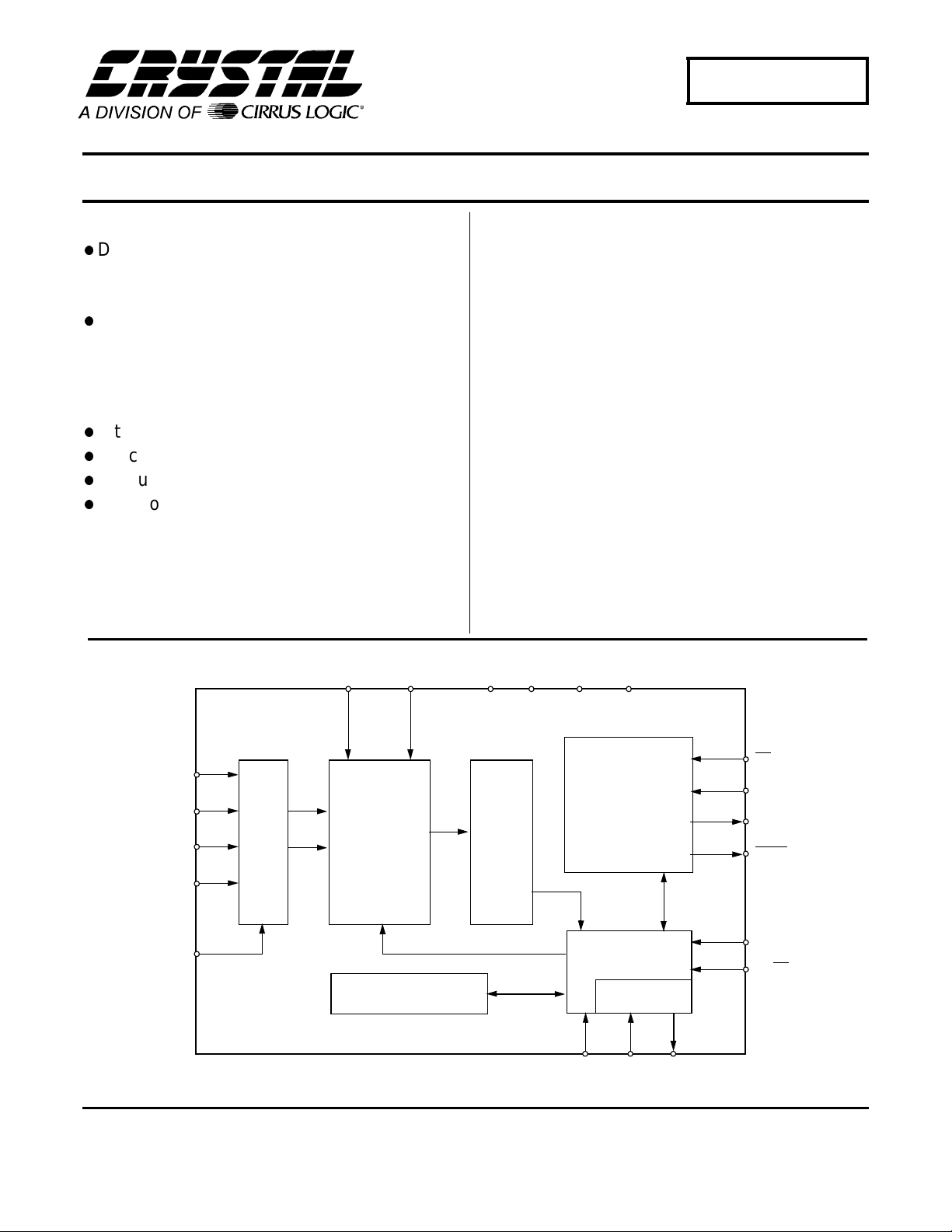
AIN1+
AIN1-
AIN2+
AIN2-
A0
VREF+ VREF- DGND VD+
12 13 16
8
10
9
11
1
MUX
4th-Order
Delta-Sigma
Modulator
Calibration SRAM
VA+
14
Digital
Filter
VA-
15
17
Serial
Interface
Logic
Calibration µC
OSC
35
CONV XIN
XOUT
2
CS
18
SCLK
19
SDATA
20
DRDY
4
CAL
7
BP/UP
6
Cirrus Logic, Inc.
Crystal Semiconductor Products Division
P.O. Box 17847, Austin, Texas 78760
(512) 445 7222 FAX: (512) 445 7581
http://www.crystal.com
Copyright Cirrus Logic, I nc. 1997
(All Rights Reserv ed)
MAR ‘95
DS126F1
1
CS5504
ANALOG CHARACTERISTICS
3.3V ± 5%; VREF+ = 2.5V, VREF- = 0V; f
(TA = T
= 32.768kHz; Bipolar Mode; R
CLK
MIN
to T
; VA+ = 5V ± 10%; VA- = -5V ± 10%; VD+ =
MAX
= 1kΩ with a 10nF to GND
source
at AIN.) (Notes 1, 2)
Parameter* Min Typ Max Units
Specified Temperature Range -40 to +85 °C
Accuracy
Linearity Error - 0.0007 0.0015
±
%FS
Differential Nonlinearity (No Missing Codes) 20 - - Bits
Full Scale Error (Note 3) -
Full Scale Drift (Note 4) Unipolar Offset (Note 3) Unipolar Offset Drift (Note 4) Bipolar Offset (Note 3) Bipolar Offset Drift (Note 4) -
±
4
±
8
±
8
±
8
±
4
±
4
±
32
-LSB
±
32
-LSB
±
16
-LSB
LSB
LSB
LSB
Noise (Referred to Output) - 2.6 - LS B
Analog Input
Analog Input Range: Unipolar (Note 5)
Bipolar
Common Mode Rejection: dc
50, 60- Hz (Note 2)
-
-
-
120
0 to +2.5
±
2.5
105
-
-
-
-
-
dB
dB
Off Channel Isolation - 120 - dB
Input Capacitance - 15 - pF
DC Bias Current (Note 1) - 5 - nA
Power Supplies
DC Power Supply Currents: I
Total
I
Analog
I
Digital
-
-
-
465
425
40
600
-
-
µ
µ
µ
Power Dissipation (Note 6) - 4.4 6.0 mW
Power Supply Rejection - 80 - dB
Notes: 1. Both source resistance and shunt capacitance are critical in determining the CS5504’s source
impedance requirements. Refer to the text s ection
Analog Input Impedance Considerations
.
2. Specifications guaranteed by design, characterization and/or test.
3. Applies after cali bration at the temperature of interest.
4. Total drift over the specified temperature range since calibration at power-up at 25 °C
5. Common mode voltage may be at any value as long as AIN+ and AIN- remain within the VA+ and
VA- supply voltages.
6. All outputs unloaded. All inputs CMOS levels.
rms
V
V
A
A
A
* Refer to the Specification Definitions immediately following the Pin Description Section.
Specifications are subject to change without notice.
2 DS126F1
DYNAMIC CHARACTERISTICS
Parameter Symbol Ratio Units
CS5504
Modulator Sampling Frequency f
Output Update Rate (CONV = 1) f
Filter Corner Frequency f
Settling Time to 1/2 LSB (FS Step) t
5V DIGITAL CHARACTERISTICS
(TA = T
MIN
to T
; VA+, VD+ = 5V ± 10%; VA- = -5V ± 10%;
MAX
DGND = 0.) (Notes 2, 7)
Parameter Symbol Min Typ Max Units
High-Level Input Voltage: XIN
All Pins Except XIN
Low-Level Input Voltage: XIN
All Pins Except XIN
High-Level Output Voltage (Note 8) V
Low-Level Output Voltage I
= 1.6 mA V
out
Input Leakage Current I
3-State Leakage Current I
Digital Output Pin Capacitance C
V
IH
V
IH
V
IL
V
IL
OH
OL
in
OZ
out
Notes: 7. All measurements are performed under static conditions.
= -100 µA. This guarantees the ability to drive one TTL load. (VOH = 2.4V @ I
8. I
out
f
s
out
-3dB
s
3.5
2.0
-
-
/2 Hz
clk
f
/1622 Hz
clk
f
/1928 Hz
clk
1/f
out
-
-
-
-
-
-
1.5
0.8
(VD+)-1.0 - - V
--0.4V
-
--
±
1
±
10
±10µ
-9-pF
= -40 µA).
out
s
V
V
V
V
µ
A
A
3.3V DIGITAL CHARACTERISTICS
(TA = T
MIN
to T
; VA+ = 5V ± 10%; VD+ = 3.3V ± 5%;
MAX
VA- = -5V ±10%; GND = 0V.) (Notes 2, 7)
Parameter Symbol Min Typ Max Units
High-Level Input Voltage: XIN
All Pins Except XIN
Low-Level Input Voltage: XIN
All Pins Except XIN
High-Level Output Voltage I
Low-Level Output Voltage I
= -400 µA
out
= 400 µA
out
Input Leakage Current I
3-State Leakage Current I
Digital Output Pin Capacitance C
V
IH
V
IH
V
IL
V
IL
V
OH
V
OL
in
OZ
out
0.7VD+
0.6VD+
-
-
-
-
-
-
-
-
0.3VD+
0.16VD+VV
V
V
(VD+)-0.3 - - V
--0.3V
-
--
±1 ±10 µA
±10 µA
-9-pF
DS126F1 3
CS5504
5V SWITCHING CHARACTERISTICS
VA- = -5V ± 10%; Input Levels: Logic 0 = 0V, Logic 1 = VD+; C
(TA = T
to T
MIN
= 50 pF.) (Note 2)
L
; VA+, VD+ = 5V ± 10%;
MAX
Parameter Symbol Min Typ Max Units
Master Clock Frequency Internal Oscillator
External Clock
XIN
f
clk
30.0
30
32.768
-
53.0
330
Master Clock Duty Cycle 40 - 60 %
Rise Times: Any Digital Input (Note 9)
Any Digital Output
Fall Times: Any Digital Input (Note 9)
Any Digital Output
t
rise
t
fall
-
-
-
-
50
20
-
1.0
-
-
1.0
-
Start-Up
Power-On Reset Period (Note 10) t
Oscillator Start-up Time XTAL = 32.768 kHz (Note 11) t
Wake-up Period (Note 12) t
res
osu
wup
-10-ms
- 500 - ms
- 1800/f
clk
-s
Calibration
CONV Pulse Width (CAL=1) (Note 13) t
CONV and CAL High to Start of Calibration t
Start of Calibration to End of Calibration t
ccw
scl
cal
100 - - ns
--2/f
- 3246/f
clk
+200 ns
clk
-s
Conversion
Set Up Time A0 to CONV High t
Hold Time A0 after CONV High t
CONV Pulse Width t
CONV High to Start of Conversion t
Set Up Time BP/UP stable prior to DRDY falling t
Hold Time BP/UP stable after DRDY falls t
Start of Conversion to End of Conversion (Note 14) t
sac
hca
cpw
scn
bus
buh
con
50 - - ns
100 - - ns
100 - - ns
--2/f
82/f
clk
--s
+200 ns
clk
0--ns
- 1624/f
clk
-s
Notes: 9. Specified using 10% and 90% points on waveform of interest.
10. An internal power-on-reset is activated whenever power is applied to the device.
11. Oscillator start-up time varies with the crystal parameters. This specification does not apply when
using an external clock source.
12. The wake-up period begins onc e the oscillator starts ; or when using an external f
, after the
clk
power-on reset time elapses.
13. Calibration can also be initiated by pulsi ng CAL high while CONV =1.
14. Conversion time will be 1622/f
if CONV remains high continuous ly.
clk
kHz
kHz
µ
s
ns
µ
s
ns
4 DS126F1

CS5504
3.3V SWITCHING CHARACTERISTICS
5%; VA- = -5V ± 10%; Input Levels: Logic 0 = 0V, Logic 1 = V D+; C
(TA = T
MIN
to T
; VA+ = 5V ± 10%; VD+ = 3.3V
MAX
= 50 pF.) (Note 2)
L
Parameter Symbol Min Typ Max Units
Master Clock Frequency Internal Oscillator
External Clock
XIN
f
clk
30.0
30
32.768
-
53.0
330
Master Clock Duty Cycle 40 - 60 %
Rise Times: Any Digital Input (Note 9)
Any Digital Output
Fall Times: Any Digital Input (Note 9)
Any Digital Output
t
rise
t
fall
-
-
-
-
50
20
-
1.0
-
-
1.0
-
Start-Up
Power-On Reset Period (Note 10) t
Oscillator Start-up Time XTAL = 32.768 kHz (Note 11) t
Wake-up Period (Note 12) t
res
osu
wup
-10-ms
- 500 - ms
- 1800/f
clk
-s
Calibration
CONV Pulse Width (CAL=1) (Note 13) t
CONV and CAL High to Start of Calibration t
Start of Calibration to End of Calibration t
ccw
scl
cal
100 - - ns
--2/f
- 3246/f
clk
+200 ns
clk
-s
Conversion
Set Up Time A0 to CONV High t
Hold Time A0 after CONV High t
CONV Pulse Widh t
CONV High to Start of Conversion t
Set Up Time BP/UP stable prior to DRDY falling t
Hold Time BP/UP stable after DRDY falls t
Start of Conversion to End of Conversion (Note 14) t
sac
hca
cpw
scn
bus
buh
con
50 - - ns
100 - - ns
100 - - ns
--2/f
82/f
clk
--s
+200 ns
clk
0--ns
- 1624/f
clk
-s
kHz
kHz
µ
s
ns
µ
s
ns
±
DS126F1 5
XIN
XIN/2
CAL
CONV
STATE
t
ccw
t
scl
t
cal
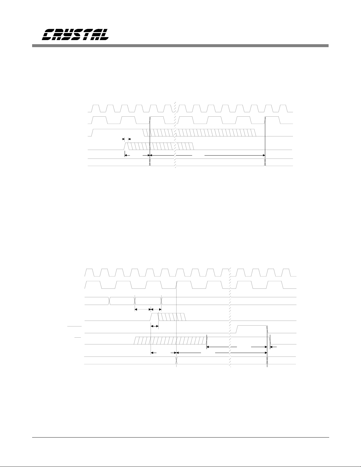
Calibration StandbyStandby
Figure 1. Calibration Timing (Not to Scale)
CS5504
XIN
XIN/2
A0
t
sac
t
hca
CONV
t
DRDY
cpw
BP/UP
t
STATE
t
scn
t
con
bus
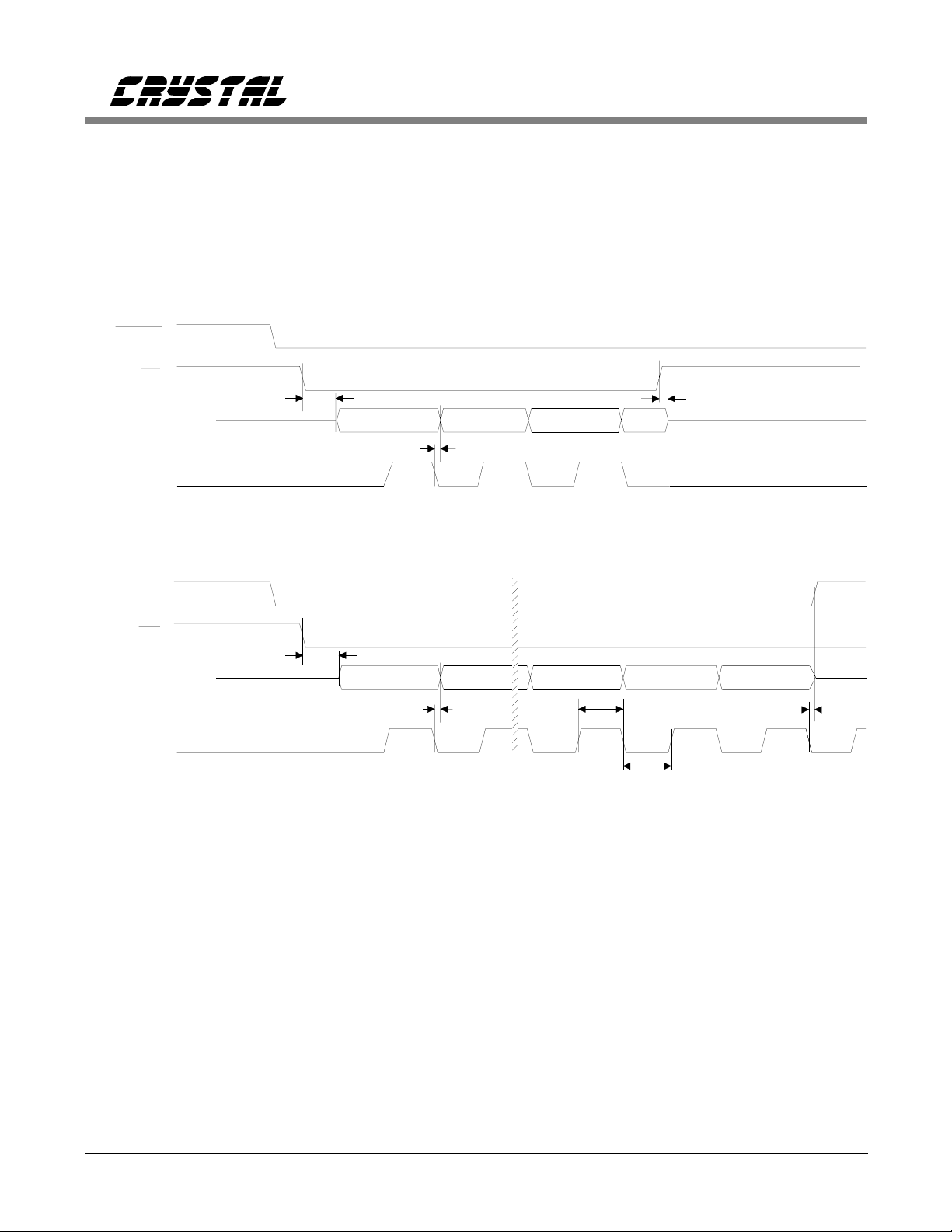
Conversion StandbyStandby
t
buh
Figure 2. Conversion Timing (Not to Scale)
6 DS126F1
CS5504
5V SWITCHING CHARACTERISTICS
(TA = T
MIN
VA- = -5V ± 10%; Input Levels: Logic 0 = 0V, Logic 1 = VD+; C
Parameter Symbol Min Typ Max Units
Serial Clock f
Serial Clock Pulse Width High
Pulse Width Low
Access Time: CS Low to data valid (Note 15) t
Maximum Delay Time: (Note 16)
SCLK falling to new SDATA bit t
Output Float Delay: CS high to output Hi-Z (Note 17)
SCLK falling to Hi-Z
Notes: 15. If
CS is activated asynchronously to DRDY, CS will not be recognized if it occurs when DRDY is high
for 2 clock cycles. The propagation delay time may be as great as 2 f
guarantee proper clocking of SDATA when usi ng asynchronous
sooner than 2/f
+ 200 ns after CS goes low.
clk
16. SDATA transitions on the falling edge of S CLK. Note that a rising SCLK must occur to enable the
serial port shifting mechanism before falli ng edges can be recognized.
CS is returned high before all data bits are output, the SDATA output will complete the current data
17. If
bit and then go to high impedance.
to T
= 50 pF.) (Note 2)
L
sclk
t
ph
t
pl
csd
dd
t
fd1
t
fd2
; VA+, VD+ = 5V ± 10%;
MAX
0-2.5MHz
200
200
- 60 200 ns
- 150 310 ns
-
-
clk
CS, SCLK should not be taken hi gh
-
-
60
160
-
-
150
300
cycles plus 200 ns. To
ns
ns
ns
ns
3.3V SWITCHING CHARACTERISTICS
(TA = T
MIN
to T
5%; VA- = -5V ± 10%; Input Levels: Logic 0 = 0V, Logic 1 = VD+; C
Parameter Symbol Min Typ Max Units
Serial Clock f
Serial Clock Pulse Width High
Pulse Width Low
Access Time: CS Low to data valid (Note 15) t
sclk
t
ph
t
pl
csd
Maximum Delay Time: (Note 16)
SCLK falling to new SDATA bit t
Output Float Delay: CS high to output Hi-Z (Note 17)
SCLK falling to Hi-Z
t
t
dd
fd1
fd2
; VA+ = 5V ± 10%; VD+ = 3.3V
MAX
= 50 pF.) (Note 2)
L
0 - 1.25 MHz
200
200
- 100 200 ns
- 400 600 ns
-
-
-
-
70
320
-
-
150
500
±
ns
ns
ns
ns
DS126F1 7
DRDY
CS
SCLK(i)
t
csd
CS5504
t
fd1
MSB-1MSB MSB-2SDATA(o) Hi-Z
t
dd
DRDY
CS
SDATA(o) Hi-Z
SCLK(i)
t
csd
MSB-1MSB LSB+2 LSB+1 LSB
t
dd
Figure 3. Timing Relationships; Serial Da ta Rea d (Not to Scale)
t
ph
t
pl
t
fd2
8 DS126F1
RECOMMENDED OPERATING CONDITIONS (DGND = 0V) (Note 18)
Parameter Symbol Min Typ Max Units
DC Power Supplies:
Positive Digital
(VA+) - (VA-)
Positive Analog
Negative Analog
Analog Reference Voltage
(Note 19)
VD+
V
diff
VA+
VA-
(VREF+)-
(VREF-)
Analog Input Voltage: (Note 20)
Unipolar
Bipolar
VAIN
VAIN0-((VREF+)-(VREF-))
Notes: 18. All vol tages with respect to ground.
19. The CS5504 can be operated wi th a reference voltage as low as 100 mV; but wi th a
corresponding reduction in noise-free resolution. The common mode voltage of the voltage reference
may be any value as long as +VREF and -VREF remain inside the supply values of VA+ and VA-.
20. The CS5504 can accept input voltages up to the analog supplies (VA+ and VA-). In unipolar mode
the CS5504 will output all 1’s if the dc input magnitude ( (AIN+)-(AIN-)) exceeds ((VREF+) -(VREF-))
and will output all 0’s if the input becomes more negativ e than 0 Volts. In bi polar mode the CS5504
will output all 1’s if the dc input magnitude ((AIN+)-(AIN-)) exceeds ((VREF+)-(VREF-)) and will output
all 0’s if the input becomes more negative in magnitude than -((VREF+)-(VREF-)).
3.15
4.5
4.5
0
5.0
10
5.0
-5.0
1.0 2.5 3.6 V
-
-
(VREF+)-(VREF-)
(VREF+)-(VREF-)VV
5.5
11
11
-5.5
CS5504
V
V
V
V
ABSOLUTE MAXIMUM RATINGS*
Parameter Symbol Min Typ Max Units
DC Power Supplies: Digital G round (Note 21)
Positive Digital (Note 22)
Positive Analog
Negative Analog
Input Current, Any Pin Except Supplies (Notes 23, 24) I
Output Current I
Power Dissipation (Total) (Note 25) - - 500 mW
Analog Input Voltage AIN and VREF pins V
Digital Input Voltage V
Ambient Operating Temperature T
Storage Temperature T
Notes: 21. No pin s hould go more positive than (VA+)+0.3V.
22. VD+ must always be less than (VA+) +0.3V, and can never exceed +6.0 V.
23. Applies to all pins including continuous overvoltage conditions at the analog input (AIN) pin.
24. Transient currents of up to 100mA will not caus e SCR latch-up. Maximum input current for a power
supply pin is ± 50 mA.
25. Total power dissipation, i ncluding all input c urrents and output currents.
* WARNING: Operation at or beyond these limits may result in permanent damage to the device.
Normal operation is not guaranteed at these extremes.
DGND
VD+
VA+
VA-
in
out
INA
IND
A
stg
-0.3
-0.3
-0.3
+0.3
--
--
-
-
-
-
(VD+)-0.3
6.0 or VA+
12
-6.0
±
10
±
25
mA
mA
(VA-)-0.3 - (VA+)+0 .3 V
-0.3 - (VD+)+0.3 V
-40 - 85 °C
-65 - 150 °C
V
V
V
V
DS126F1 9

CS5504
GENERAL DESCRIPTION
The CS5504 is a low power, 20-bit, monolithic
CMOS A/D converter designed specifically for
measurement of dc signals. The CS5504 includes a delta-sigma charge-balance converter, a
voltage reference, a calibration micro controller
with SRAM, a digital filter a nd a seria l interface.
The CS5504 is optimized to operate from a
32.768 kHz crystal but can be driven by an external clock whose frequency is between 30 kHz
and 330 kHz. When the digital filter is operated
with a 32.768 kHz clock, the filter has zeros precisely at 50 and 60 Hz line frequencies and
multiples thereof.
The CS5504 uses a "start convert" command to
latch the input channel selection and to start a
convolution cycle on the digital filter. Once the
filter cycle is completed, the output port is updated. When operated with a 32.768 kHz clock
the ADC converts and updates its output port at
20 samples/sec. The output port operates in a
synchronous externally-clocked interface format.
tion of this command will not occur until the
complete wake-up period elapses. If no command is given, the device enters the standby
state.
Calibration
After the initial application of power, the
CS5504 must enter the calibration state prior to
performing accurate conversions. During calibration, the chip executes a two-step process. The
device first performs an offset calibration and
then follows this with a gain calibration. The
two calibration steps determine the zero reference point and the full scale reference point of
the converter’s transfer function. From these
points it calibrates the zero point and a gain
slope to be used to properly scale the output
digital codes when doing conversions.
The calibration state is entered whenever the
CAL and CONV pins are high at the same time.
The state of the CAL and CONV pins at poweron are recognized as commands, but will not be
executed until the end of the 1800 clock cycle
wake-up period.
THEORY OF OPERATION
If CAL and CONV become active (high) during
the 1800 clock cycle wake-up time, the con-
Basic Converter Operation
verter will wait until the wake-up period elapses
before executing the calibration. If the wake-up
The CS5504 A/D converter has three operating
states. These are stand-by, calibration, and conversion. When power is first applied, an internal
power-on reset delay of about 10 ms resets all of
the logic in the device. The oscillator must then
begin oscillating before the device can be considered functional. After the power-on reset is
time has elapsed, the converter will be in the
standby mode waiting for instruction and will
enter the calibration cycle immediately if CAL
and CONV become active. The calibration lasts
for 3246 clock cycles. Calibration coefficients
are then retained in the SRAM (static RAM) for
use during conversion.
applied, the device enters the wake-up period for
1800 clock cycles after clock is present. This
allows the delta-sigma modulator and other circuitry (which are operating with very low
The states of A0 and BP/UP are ignored during
calibration but should remain stable throughout
the calibration period to minimize noise.
currents) to reach a stable bias condition prior to
entering into either the calibration or conversion
states. During the 1800 cycle wake-up period,
the device can accept an input command. Execu-
10 DS126F1
When conversions are performed in unipolar
mode or in bipolar mode, the converter uses the
same calibration factors to compute the digital

CS5504
output code. The only difference is that in bipolar mode the on-chip microcontroller offsets the
computed output word by a code value of
8000H. This means that the bipolar measurement range is not calibrated from full scale
positive to full scale negative. Instead it is calibrated from the bipolar zero scale point to full
scale positive. The slope factor is then extended
below bipolar zero to accommodate the negative
input signals. The converter can be used to convert both unipolar and bipolar signals by
changing the BP/UP pin. Recalibration is not required when switching between unipolar and
bipolar modes.
At the end of the calibration cycle, the on-chip
micro controller checks the logic state of the
CONV signal. If the CONV input is low the device will enter the standby mode where it waits
for further instruction. If the CONV signal is
high at the end of the calibration cycle, the converter will enter the conversion state and
perform a conversion on the input channel. The
CAL signal can be returned low any time after
calibration is initiated. CONV can also be returned low, but it should never be taken low and
then taken back high until the calibration period
has ended and the converter is in the standby
state. If CONV is taken low and then high
again with CAL high while the converter is calibrating, the device will interrupt the current
calibration cycle and start a new one. If CAL is
taken low and CONV is taken low and then high
during calibration, the calibration cycle will
continue as the conversion command is disregarded. The state of BP/UP is not important
during calibrations.
If an "end of calibration" signal is desired, pulse
the CAL signal high while leaving the CONV
signal high continuously. Once the calibration is
completed, a conversion will be performed. At
the end of the conversion, DRDY will fall to indicate the first valid conversion after the
calibration has been completed.
Conversion
The conversion state can be entered at the end of
the calibration cycle, or whenever the converter
is idle in the standby mode. If CONV is taken
high to initiate a calibration cycle ( CAL also
high), and remains high until the calibration cycle is compl eted (CAL is taken low after CON V
transitions high), the converter will begin a conversion upon completion of the calibration
period. The device will perform a conversion on
the input channel selected by A0 when CONV
transitions high. Table 1 indicates the multiplexer channel selection truth table.
A0 Channel Addressed
0AIN1
1AIN2
Table 1. Multiplexer Truth Table
The A0 input is latched internal to the CS5504
when CONV rises. A0 has internal pull-down
circuits which default the multiplexer to channel
AIN1.
The BP/UP pin is not a latched input. The
BP/UP pin controls how the output word from
the digital filter is processed. In bipolar mode
the output word computed by the digital filter is
offset by 80000H (see Understanding Converter
Calibration). BP/UP can be changed after a conversion is started as long as it is stable for 82
clock cycles of the conversion period prior to
DRDY falling. If one wishes to intermix measurement of bipolar and unipolar signals on
various input channels, it is best to switch the
BP/UP pin immediately after DRDY falls and
leave BP/UP stable until DRDY falls again.
The digital filter in the CS5504 has a Finite Impulse Response and is designed to settle to full
accuracy in one conversion time.
If CONV is left high, the CS5504 will perform
continuous conversions. The conversion time
will be 1622 clock cycles. If conversion is initi-
DS126F1 11

CS5504
ated from the standby state, there may be up to
two XIN clock cycles of uncertainty as to when
conversion actually begins. This is because the
internal logic operates at one half the external
clock rate and the exact phase of the internal
clock may be 180° out of phase relative to the
XIN clock. When a new conversion is initiated
from the standby state, it will take up to two
XIN clock cycles to begin. Actual conversion
will use 1624 clock cycles before DRDY goes
low to indicate that the serial port has been updated. See the Serial Interface Logic section of
the data sheet for information on reading data
from the serial port.
In the event the A/D conversion command
(CONV going positive) is issued during the conversion state, the current conversion will be
terminated and a new conversion will be initiated.
Voltage Reference
The CS5504 uses a differential voltage referenc e
input. The positive input is VREF+ and the
negative input is VREF-. The voltage between
VREF+ and VREF- can range from 1 volt minimum to 3.6 volts maximum. The gain slope will
track changes in the reference without recalibration, accommodating ratiometric applications.
Analog Input Range
The analog input range is set by the magnitude
of the voltage between the VREF+ and VREFpins. In unipolar mode the input range will
equal the magnitude of the voltage reference. In
bipolar mode the input voltage range will equate
to plus and minus the magnitude of the voltage
reference. While the voltage reference can be as
great as 3.6 volts, its common mode voltage can
be any value as long as the reference inputs
VREF+ and VREF- stay within the supply voltages for the A/D. The differential input voltage
can also have any common mode value as long
as the maximum signal magnitude stays within
the supply voltages.
The A/D converter is intended to measure dc or
low frequency inputs. It is designed to yield accurate conversions even with noise exceeding
the input voltage range as long as the spectral
components of this noise will be filtered out by
the digital filter. For example, with a 3.0 volt
reference in unipolar mode, the converter will
accurately convert an input dc signal up to
3.0 volts with up to 15% overrange for 60 Hz
noise. A 3.0 volt dc signal could have a 60 Hz
component which is 0.5 volts above the maximum input of 3.0 (3.5 volts peak; 3.0 volts dc
plus 0.5 volts peak noise) and still accurately
convert the input signal (XIN = 32.768 kHz).
This assumes that the signal plus noise amplitude stays within the supply voltages.
The CS5504 converters output data in binary
format when converting unipolar signals and in
offset binary format when converting bipolar
signals. Table 2 outlines the output coding for
both unipolar and bipolar measurement modes.
Unipolar Input
Voltage
>(VREF - 1.5 LSB) FFFFF >(VREF - 1.5 LSB )
VREF - 1.5 LSB FFFFF
VREF/2 - 0.5 LSB
+ 0.5 LSB
<(+ 0.5 LSB) 00000 <(VREF + 0.5 LSB)
Note: Table excludes common mode volt age on the
signal and reference inputs.
Table 2. Output Coding
Output
Codes
FFFFE
80000
7FFFF
00001
00000
Bipolar Input
Voltage
VREF - 1.5 LSB
-0.5 LSB
-VREF + 0.5 LSB
12 DS126F1

CS5504
Converter Performance
The CS5504 A/D converter has excellent linearity performance. Calibration minimizes the
errors in offset and gain. The CS5504 device
has no missing code performance to 20-bits.
The converter achieves Common Mode Rejection (CMR) at dc of 105 dB typical, and CMR at
50 and 60 Hz of 120 dB typical.
The CS5504 can experience some drift as temperature changes. The CS5504 uses
chopper-stabilized techniques to minimize drift.
Measurement errors due to offset or gain drift
can be eliminated at any time by recalibrating
the converter.
Analog Input Impedance Considerations
The analog input of the CS5504 can be modeled
as illustrated in Figure 4 (the model ignores the
multiplexer switch resistance). Capacitors (15 pF
each) are used to dynamically sample each of
the inputs (AIN+ and AIN-). Every half XIN cycle the switch alternately connects the capacitor
to the output of the buffer and then directly to
the AIN pin. Whenever the sample capacitor is
switched from the output of the buffer to the
AIN pin, a small packet of charge (a dynamic
demand of current) is required from the input
source to settle the voltage of the sample capaci-
AIN+
15 pF
Internal
Bias
Voltage
15 pF
AIN-
V
V
os
os
≤
≤
100 mV
100 mV
+
-
+
-
tor to its final value. The voltage on the output
of the buffer may differ up to 100 mV from the
actual input voltage due to the offset voltage of
the buffer. Timing allows one half of a XIN
clock cycle for the voltage on the sample capacitor to settle to its final v alue.
An equation for the maximum acceptable source
resistance is derived.
−
Rs
max
=
2XI N
(
15p F + C
EXT
1
+
15pF(
(
15pF
V
e
100mv
+
C
EXT
)
)
)
ln
Ve
This equation assumes that the offset voltage of
the buffer is 100 mV, which is the worst case.
The value of Ve is the maximum error voltage
which is acceptable. C
is the combination
EXT
of any external or stray capacitance.
For a maximum error voltage (Ve) of 600 nV in
the CS5504 (1/4LSB at 20-bits), the above equation indicates that when operating from a
32.768 kHz XIN, source resistances up to 84 kΩ
in the CS5504 are acceptable in the absence of
external capacitance (C
EXT
= 0).
The VREF+ and VREF- inputs have nearly the
same structure as the AIN+ and AIN- inputs.
Therefore, the discussion on analog input impedance applies to the voltage reference inputs as
well.
Digital Filter Characteristics
The digital filter in the CS5504 is the combination of a comb filter and a low pass filter. The
comb filter has zeros in its transfer function
which are optimally placed to reject line interference frequencies (50 and 60 Hz and their
multiples) when the CS5504 is clocked at
Figure 4. Analog Input Model
DS126F1 13

CS5504
0
-20
X1 = 32.768kHz
X2 = 330.00kHz
-40
-60
-80
-100
Attenuation (dB)
-120
-140
XIN = 32.768 kHz
-160
X1
0
X2
040402.8380805.66
120
1208.5
160
1611.3
Frequency (Hz)
Figure 5. Filter Ma gnitude Plot to 260 Hz
0
-20
-40
-60
-80
Attenuation (dB)
-100
-120
Flatness
Frequency
1
2
3
4
5
6
7
8
9
10
17
dB
-0.010
-0.041
-0.093
-0.166
-0.259
-0.374
-0.510
-0.667
-0.846
-1.047
-3.093
XIN = 32.768 kHz
200
2014.2
240
2416.9
Frequency
(Hz)
50 125.6
60 126.7
100 145.7
120 136.0
150 118.4
180 132.9
200 102.5
240 108.4
Notch
Depth
(dB)
Frequency
(Hz)
50±1%
60±1%
100±1%
120±1%
150±1%
180±1%
200±1%
240±1%
Minimum
Attenuation
(dB)
55.5
58.4
62.2
68.4
74.9
87.9
94.0
104.4
Table 3. Filter Notch Attenuation (XIN = 32.768 kHz)
180
135
90
45
0
-45
Phase (Degrees)
-90
XIN = 32.768 kHz
-135
-140
0 5 10 15 20 25 30 35 40 45 50
Frequency (Hz)
Figure 6. Filter Magnitude Plot to 50 Hz
32.768 kHz. Figures 5, 6 and 7 illustrate the
magnitude and phase characteristics of the filter.
Figure 5 illustrates the filter attenuation from dc
to 260 Hz. At exactly 50, 60, 100, and 120 Hz
the filter provides over 120 dB of rejection. Table 3 indicates the filter attenuation for each of
the potential line interference frequencies when
-180
0 5 10 15 20 25 30 35 40 45 50
Frequen cy (Hz)
Figure 7. Filter Phase Plot to 50 Hz
of these interference frequencies even if the fundamental line frequency should vary ± 1% from
its specified frequency. The -3dB corner frequency of the filter when operating from a
32.768 kHz clock is 17 Hz. Figure 7 illustrates
that the phase characteristics of the filter are precisely linear phase.
the converter is operating with a 32.768 kHz
clock. The converter yields excellent attenuation
14 DS126F1

CS5504
If the CS5504 is operated at a clock rate other
than 32.768 kHz, the filter characteristics, including the comb filter zeros, will scale with the
operating clock frequency. Therefore, optimum
rejection of line frequency interference will occur with the CS5504 running at 32.768 kHz.
Anti-Alias Con sideratio ns for Spec tral
Measurement Applications
Input frequencies greater than one half the output word rate (CONV = 1) may be aliased by
the converter. To prevent this, input signals
should be limited in frequency to no greater than
one half the output word rate of the converter
(when
CONV =1). Frequencies close to the modulator
sample rate (XIN/2) and multiples thereof may
also be aliased. If the signal source includes
spectral components above one half the output
word rate (when CONV = 1) these components
should be removed by means of low-pass filtering prior to the A/D input to prevent aliasing.
Spectral components greater than one half the
output word rate on the VREF inputs (VREF+
and VREF-) may also be aliased. Filtering of the
reference voltage to remove these spectral components from the reference voltage is desirable.
Crystal Oscillator
The CS5504 is designed to be operated using a
32.768 kHz "tuning fork" type crystal. One end
of the crystal should be connected to the XIN
input. The other end should be attached to
XOUT. Short lead lengths should be used to
minimize stray capacitance.
Over the industrial temperature range (-40 to
+85 °C) the on-chip gate oscillator will oscillate
with other crystals in the range of 30 kHz to 53
kHz. The chip will operate with external clock
frequencies from 30 kHz to 330 kHz over the industrial temperature range. The 32.768 kHz
crystal is normally specified as a time-keeping
crystal with tight specifications for both initial
frequency and for drift over temperature. To
maintain excellent frequency stability, these
crystals are specified only over limited operating
temperature ranges (i.e. -10 °C to +60 °C) by the
manufacturers. Applications of these crystals
with the CS5504 does not require tight initial
tolerance or low tempco drift. Therefore, a lower
cost crysta l with looser init ial tolerance a nd tempco will generally be adequate for use with the
CS5504. Also check with the manufacturer
about wide temperature range application of
their standard crystals. Generally, even those
crystals specified for limited temperature range
will operate over much larger ranges if frequency stability over temperature is not a
requirement. The frequency stability can be as
bad as ±3000 ppm over the operating temperature range and still be typically better than the
line frequency (50 Hz or 60 Hz) stability over
cycle-to-cycle during the course of a day.
Serial Interface Logic
The digital filter in the CS5504 takes 1624 clock
cycles to compute an output word once a conversion begins. At the end of the conversion
cycle, the filter will attempt to update the serial
port. Two clock cycles prior to the update
DRDY will go high. When DRDY goes high
just prior to a port update it checks to see if the
port is either empty or unselected (CS = 1). If
the port is empty or unselected, the digital filter
will update the port with a new output word.
When new data is put into the port DRDY will
go low.
Reading Serial Data
SDATA is the output pin for the serial data.
When CS goes low after new data becomes
available (DRDY goes low), the SDATA pin
comes out of Hi-Z with the MSB data bit present. SCLK is the input pin for the serial clock.
If the MSB data bit is on the SDATA pin, the
DS126F1 15

CS5504
first rising edge of SCLK enables the shifting
mechanism. This allows the falling edges of
SCLK to shift subsequent data bits out of the
port. Note that if the MSB data bit is output and
the SCLK signal is high, the first falling edge of
SCLK will be ignored because the shifting
mechanism has not become activated. After the
first rising edge of SCLK, each subsequent falling edge will shift out the serial data. Once the
LSB is present, the falling edge of SCLK will
cause the SDATA output to go to Hi-Z and
DRDY to return high. The serial port register
will be updated with a new data word upon the
completion of another conversion if the serial
port has been emptied, or if the CS is inactive
(high).
CS can be operated asynchronously to the
DRDY signal. The DRDY signal need not be
monitored as long as the CS signal is taken low
for at least two XIN clock cycles plus 200 ns
prior to SCLK being toggled. This ensures that
CS has gained control over the serial port.
Power Supplies and Grounding
The analog and digital supply pins to the
CS5504 are brought out on separate pins to
minimize noise coupling between the analog and
digital sections of the chip. Note that there is no
analog ground pin. No analog ground pin is required because the inputs for measurement and
for the voltage reference are differential and require no ground. In the digital section of the
chip the supply current flows into the VD+ pin
and out of the DGND pin. As a CMOS device,
the CS5504 requires that the supply voltage on
the VA+ pin always be more positive than the
voltage on any other pin of the device. If this
requirement is not met, the device can latch-up
or be damaged. In all circumstances the VA+
voltage must remain more positive than the VD +
or DGND pins; VD+ must remain more positive
than the DGND pin.
The following power supply options are possible:
VA+ = +5V to +10V, VA- = 0V, VD+ = +5V
VA+ = +5V, VA- = -5V, VD+ = +5V
VA+ = +5V, VA- = 0V to -5V, VD+ = +3.3V
The CS5504 cannot be operated with a 3.3V
digital supply if VA+ is greater than +5.5V.
Figure 8 illustrates the System Connection Diagram for the CS5504 using a single +5V supply.
Note that all supply pins are bypassed with
0.1 µF capacitors and that the VD+ digital sup-
ply is derived from the VA+ supply.
Figure 9 illustrates the CS5504 using dual supplies of +5 and -5V.
Figure 10 illustrates the CS5504 using dual supplies of +10V analog and +5V digital.
When using separate supplies for VA+ and
VD+, VA+ must be established first. VD+
should never become more positive than VA+
under any operating condition. Remember to investigate transient power-up conditions, when
one power supply may have a faster rise time.
16 DS126F1

10
CS5504
Ω
+5V
Analog
Supply
Analog*
Signal
Sources
Voltage
Reference
0.1
µ
F
Calibration
Control
Bipolar/
Unipolar
Input Select
*Unused analog inputs should
be tied to signal ground
+
-
10
11
12
13
4
7
8
9
VA+
CAL
BP/UP
AIN1+
AIN1-
AIN2+
AIN2-
VREF+
VREF-
14
CS5504
17
VD+
XIN
XOUT
SCLK
SDATA
DRDY
CS
A0
CONV
5
6
18
19
20
2
1
3
0.1
µ
32.768 kHz
F
Optional
Clock
Source
Serial
Data
Interface
Control
Logic
16
Unused Logic
inputs must be
connected to
VD+ or DGND
VA-
DGND
15
Figure 8. CS5504 System Connection Diagram Us ing Single Supply
DS126F1 17

10
CS5504
Ω
+5V
Analog
Supply
Analog*
Signal
Sources
Voltage
Reference
0.1
µ
F
Calibratio n
Control
Bipolar/
Unipolar
Input Select
*Unused analog inputs should
be tied to signal ground
+
-
10
11
12
13
4
7
8
9
VA+
CAL
BP/UP
AIN1+
AIN1-
AIN2+
AIN2-
VREF+
VREF-
14
CS5504
17
VD+
XIN
XOUT
SCLK
SDATA
DRDY
CS
A0
CONV
5
6
18
19
20
2
1
3
0.1
µ
32.76 8 kHz
F
Optional
Clock
Source
Serial
Data
Interface
Control
Logic
16
Unused Logic
inputs must be
connected to
VD+ or DGND
-5V
Analog
Supply
0.1
µ
F
VA-
DGND
15
Figure 9. CS5504 System Connection Diagram Using Dual Supplies
18 DS126F1

Note: VD+ should never be more positive than VA+
CS5504
+10V
Analog
Supply
Analog*
Signal
Source s
Voltage
Reference
0.1
F
µ
Calibration
Control
Bipolar/
Unipolar
Input Select
*Unused analog inputs should
be tied to signal ground
+
-
10
11
12
13
4
7
8
9
CAL
BP/UP
AIN1+
AIN1-
AIN2+
AIN2-
VREF+
VREF-
14
CS5504
VA-
15
17
VD+VA+
XIN
XOUT
SCLK
SDATA
DRDY
CS
A0
CONV
DGND
5
6
18
19
20
2
1
3
16
0.1
µ
32.768 kHz
F
+5V
Digital
Supply
Optional
Clock
Source
Serial
Data
Interface
Control
Logic
Unused Logi c
inputs must be
connected to
VD+ or DGND
Figure 10. CS5504 System Connection Diagram Us ing Dual Supply,
+10V Analog, +5V Digital
Schematic & Layout Review Service
Confirm Optimum
Confirm Optimum
Schematic & Layout
Schematic & Layout
Before Building Your Board.
Before Building Your Board.
For Our Free Review Service
For Our Free Review Service
Call Applications Engineering.
Call Applications Engineering.
Call:(512) 445-7222
DS126F1 19

PIN DESCRIPTIONS*
CS5504
MULTIPLEXER SELECTION INPUT A0 DRDY DATA READY
CHIP SELECT
CONVERT CONV SCLK SE RIAL CLOCK INPUT
CALIBRATE CAL VD+ POSITIVE DIGITAL P OWER
CRYSTAL IN XIN DGND DIGITAL GROUND
CRYSTAL OUT XOUT VA- NEGATIVE ANALOG POWER
BIPOLAR/UNIPOLAR BP/
DIFFERENTIAL ANALOG INPUT AIN1+ VREF- VOLTAGE REFERENCE INP UT
DIFFERENTIAL ANALOG INPUT AIN2+ VREF+ VOLTAGE REFERENCE INPUT
DIFFERENTIAL ANALOG INPUT AIN1- AIN2- DIFFERENTIAL ANALOG INPUT
*Pinout applies to both PDIP and SOIC
CS SDATA SERIAL DATA OUTPUT
UP VA+ POSITIVE ANALOG POWE R
1
2
3
4
5
6
7
8
9
10
20
19
18
17
16
15
14
13
12
11
Clock Generator
XIN; XOUT - Crystal In; Crystal Out, Pins 5, 6.
A gate inside the chip is connected to these pins and can be used with a crystal to provide the
master clock for the device. Alternatively, an external (CMOS compatible) clock can be
supplied into the XIN pin to provide the master clock for the device. Loss of clock will put the
device into a lower powered state (approximately 70% power reduction).
Serial Output I/O
CS - Chip Select, Pin 2.
This input allows an external device to access the serial port.
DRDY - Data Ready, Pin 20.
Data Ready goes low at the end of a digital filter convolution cycle to indicate that a new
output word has been placed into the serial port. DRDY will return high after all data bits are
shifted out of the serial port or two master clock cycles before new data becomes available if
the CS pin is inactive (high).
SDATA - Serial Data Output, Pin 19.
SDATA is the output pin of the serial output port. Da ta from this pin will be output at a rate
determined by SCLK. Data is output MSB first and advances to the next data bit on the falling
edges of SCLK. SDATA will be in a high impedance state when not transmitting data.
SCLK - Serial Clock Input, Pin 18.
A clock signal on this pin determines the output rate of the data from the SDATA pin. This pin
must not be allowed to float.
20 DS126F1

Control Input Pins
CAL - Calibrate, Pin 4.
When taken high the same time that the CONV pin is taken high the c onverter will perform a
self-calibration which includes calibration of the offset and gain scale factors in the converter.
CONV - Convert, Pin 3.
The CONV pin initiates a calibration cycle if it is taken from low to high while the CAL pin is
high, or it initiates a conversion if it is taken from low to high with the CAL pin low. If
CONV is held high (CAL low) the converter will do continuous conversions.
BP/UP - Bipolar/Unipolar, Pin 7.
The BP/UP pin selects the conversion mode of the converter. When high the converter will
convert bipolar input signals; when low it will convert unipolar input signals.
A0 - Multiplex er Selecti on Input, Pin 1.
Selects the input channel for conversion. A0=0=AIN1. A0 is latched when CONV transitions
from low to high. This input has a pull-down resistor internal to the chip.
CS5504
Measurement and Reference Inputs
AIN1+, AIN2+, AIN1-, AIN2- - Differential Analog Inputs, Pins 8, 9, 10, 11.
Analog differential inputs to the delta-sigma modulator.
VREF+, VREF- - Differential Voltage Reference Inputs, Pins 12, 13.
A differential voltage reference on these pins operates as the voltage reference for the
converter. The voltage between these pins can be any voltage between 1.0 and 3.6 volts.
Power Supply Connections
VA+ - Positive Analog Power, Pin 14.
Positive analog supply voltage. Nominally +5 volts.
VA- - Negative Analog Power, Pin 15.
Negative analog supply voltage. Nominally -5volts.
VD+ - Positive Digital Power, Pin 17.
Positive digital supply voltage. Nominally +5 volts or +3.3 volts.
DGND - Digital Ground, Pin 16.
Digital Ground.
DS126F1 21

SPECIFICATION DEFINITIONS
Linearity Error
The deviation of a code from a straight line which connects the two endpoints of the A/D
Converter transfer function. One endpoint is located 1/2 LSB below the first code transition
and the other endpoint is located 1/2 LSB beyond the code transition to all ones. Units in
percent of full-scale.
Differential Nonlinearity
The deviation of a code’s width from the ideal width. Units in LSBs.
Full Scale Error
The deviation of the last code transition from the ideal [{(VREF+) - (VREF-)} - 3⁄2 LSB].
Units are in LSBs.
Unipolar Offset
The deviation of the first code transition from the ideal (1⁄2 LSB above the voltage on the AINpin.) when in unipolar mode (BP/UP low). Units are in LSBs.
CS5504
Bipolar Offset
The deviation of the mid-scale transition (011...111 to 100...000) from the ideal (1⁄2 LSB below
the voltage on the AIN- pin.) when in bipolar mode (BP/UP high). Units are in LSBs
22 DS126F1

CS5504
APPENDIX
The following companies provide 32.768 kHz crystals in many package varieties and temperature
ranges.
Fox Electronics
5570 Enterprise Parkway
Fort Meyers, FL 33905
(813) 693-0099
Micro Crystal Division / SMH
702 West Algonquin Road
Arlington Heights, IL 60005
(708) 806-1485
SaRonix
4010 Transport Street
Palo Alto, California 94303
(415) 856-6900
Statek
512 North Main
Orange, California 92668
(714) 639-7810
IQD Ltd.
North Street
Crewkerne
Somerset TA18 7AK
England
01460 77155
Taiwan X’ta l Corp.
5F. No. 16, Sec 2, Chung Yang S. RD.
Reitou, Taipei, Taiwan R. O. C.
Tel: 02-894-1202
Fax: 02-895-6207
Interquip Limited
24/F Million Fortune Industrial Centre
34-36 Chai Wan Kok Street, Tsuen Wan N T
Tel: 4135515
Fax: 4137053
S& T Enterprises, Ltd.
Rm 404 Blk B
Sea View Estate
North Point, Hong Kong
Tel: 5784921
Fax: 8073126
Mr. Darren Mcleod
Hy-Q International Pty. Ltd.
12 Rosella Road,
FRANKSON, 3199
Victoria, Australia
Tel: 61-3-783 9611
Fax: 61-3-783 9703
Mr. Pierre Hersberger
Microcrystal/DIV. ETA S.A.
Schild-Rust-Strasse 17
Grenchen CH-2540
Switzerland
065 53 05 57
DS126F1 23

• Notes •

CDB5504
Evaluation Board for CS5504 A/D Converter
Features
l
Operation with on-board 32.768 kHz crystal
or off-board clock source
l
DIP Switch Selectable:BP/UP mode;
Channel selection
l
On-board precision voltage reference
l
Access to all digital control pins
I
AIN2-
AIN2+
AIN1-
AIN1+
Description
The CDB5504 is a circuit board designed to provide
quick evaluation of the CS5504 A/D converter.
The board prov ides buffered digital signals , an on-board
precision volt age reference, o ptions for usi ng an externa l
clock, and a momentary switch to initiate calibra tion.
ORDERING INFORMATION
CDB5504 Evaluation Board
CS 5504
B
U
F
F
E
R
S
H
E
A
D
E
R
VREF
Cirrus Logic, Inc.
Crystal Semiconductor Products Division
P.O. Box 17847, Austin, Texas 78760
(512) 445 7222 FAX: (512) 445 7581
http://www.crystal.com
+5V GND
Copyright Cirrus Logic, I nc. 1998
-5 V
(All Rights Reserv ed)
CLKIN
MAR ‘95
DS126DB1
25

Introduction
CDB5504
The CDB5504 evaluation board provides a quick
means of testing the CS5504 A/D converter. The
CS5504 converter require a minimal amount of
external circuitry. The evaluation board comes
configured with the A/D converter chip operating from a 32.768 kHz crystal and with an
off-chip precision 2.5 volt reference. The board
provides access to all of the digital interface pins
of the CS5504 chip.
The board is configured for operation from +5
and -5 volt power supplies, but can be operated
from a single +5 volt supply if the -5V binding
post is shorted to the GND binding post.
Evaluation Board Overview
The board provides a complete means of making
the CS5504 A/D converter chip function. The
user must provide a means of taking the output
data from the board in serial format and using it
in his system.
Figure 1 illustrates the schematic for the board.
The board comes configured for the A/D converter chip to operate from the 32.768 kHz
watch crystal. A BNC connector for an external
clock is provided on the board. To connect the
external BNC source to the converter chip, a circuit trace must be cut. Then a jumper must be
inserted in the proper holes to connect the XIN
pin of the converter to the input line from the
BNC. The BNC input is terminated with a 50Ω
resistor. Remove this resistor if driving from a
logic gate. See the schematic in Figure 1.
and U3 are used to buffer the conve rter for interface to off-board circuits. The buffers are used
on the evaluation board only because the exact
loading and off-board circuitry is unknown.
Most applications will not require the buffer ICs
for proper operation.
To put the board in operation, select either bipolar or unipolar mode with DIP switch S2. Then
press the CAL pushbutton after the board is
powered up. This initiates calibration of the converter which is required before measurements
can be taken.
To select an input, one of two channels, use DIP
switch S2 to select the input for A0 (see Table 1). Once A0 is selected, the CONV switch
(S2-3) must be switched on (closed) and then
open to cause the CONV signal to transition low
to high. This latches the A0 channel selection
into the converter. With CONV high (S2-3 open)
the converter will convert continuously.
Figure 3 illustrates the CAB5504 adapter board.
The CAB5504 translates a CS5505 pinout to a
CS5504 pinout.
Figures 4 and 5 illustrate the evaluation board
layout while Figure 6 illustrates the component
placement (silkscreen) of the evaluation board.
The board comes with the A/D converter
VREF+ and VREF- pins hard-wired to the
2.5 volt bandgap voltage reference IC on the
A0 Channel Addressed
0AIN1
1AIN2
board.
Table 1. Multiplexer Truth Table
All of the control pins of the CS5504 are available at the J1 header connector. Buffer ICs U2
26 DS126DB1

DS126DB1 27
+5V
GND
-5V
D1
6.8V
D2
6.8V
External
VREF
AIN2-
AIN2+
AIN1-
AIN1+
+
+
+5
0.1 µF
C2
10 µF
C3
10
C9
+
_
R28
100k
R29
100k
R30
100k
R31
100k
R22
+5
CAL
C11
0.01 µF
11
13
C17
0.1 µF
R23
100k
R24
100k
R25
100k
U3D
R10
14
R16
12
10
VD+
1
2
4
6
VD+
20k
U2A
U2B
U2C
U2D
U2E
U2F
8
100k
R11
100k
R17
47k
3
5
VD+
R18
R19
100k
VD+
R20
100k
4
14
3
7
8
47k
VD+
U3A
1
U3C
10
7
9
1211
15
56
U3B
R21
47k
2
VD+
9
Note: Buffers not required for general applications.
VD+
SDATA
Y1
32.768
kHz
17
CAL
CONV
CS
A0
DRDY
SCLK
BP/UP
VD+
C10
0.1 µF
4
TP10
3
TP9
2
TP8
1
TP7
TP11
20
TP12
19
TP13
18
TP14
7
+5
C7
1A
1B
2A
2B
3A
3B
0.01 µF
R2
200
R3
50
0.1 µF
R27
1K
R26
1K
C15
0.01 µF
12
C19
10nF
13
C20
10nF
TP3
11
TP4
9
TP5
10
TP6
8
TP15
VA- DGND
-5
C1
µ
F
0.1
+5
C5
0.1 µF
C4
0.1 µF
µ
F
2
LT1019
-2.5 V
4
402
R7
402
R6
402
R5
402
R4
6
5
C12
0.01 µF
R8
25k
AGND
DGND
- 5
C8
C13
0.1 µF
C14
0.01 µF
CLKIN
R9
10
14
VA+
VREF+
VREF-
U1
CS5504
AIN2-
AIN2+
AIN1-
AIN1+
XIN XOUT
15 16
56
VD+
0.1 µF
C18
R1
100k
+
C16
10
10 µF
S2
+5
+5
DRDY
SCLK
SDATA
J2
CAL
CONV
CS
A0
A1
DRDY
SDATA
SCLKO
SCLKI
BP/UP
J1
U2 74HC4050
U3 74HC125
A1
A0
CONV
BP/UP
CDB5504
Figure 1. ADC Connections

CDB5504
A0
CS SDATA
CONV SCLK
CAL VD+
XIN DGND
XOUT VA-
UP VA+
BP/
AIN1+ VREFAIN2+ VREF+
AIN1- AIN2-
1
2
3
4
5
6
7
8
9
10
20
19
18
17
16
15
14
13
12
11
DRDY
Figure 2. CS5504 Pin Layout
11
20 14
101211
13
Figure 3. CAB5504 Adapter Board
28 DS126DB1

CDB5504
Figure 4. Top Ground Plane Layer (NOT TO SCALE)
DS126DB1 29

CDB5504
Figure 5. Bottom Trace Layer (NOT TO SCALE)
30 DS126DB1

CDB5504
AIN-
AIN1+
AIN1-
AIN2+
AIN2-
CDB5504
Figure 6. Silk Screen Layer (NOT TO SCALE)
DS126DB1 31

 Loading...