

CS5460
Single Phase Bi-Directional Power/Energy IC
Features
l Energy Data Linearity: 0.1% of Reading over
1000:1 Dynamic Range
l On-Chip Functions: Energy, I ∗ V,
I
and V
RMS
Conversion
l Complies with IEC 687/1036, JIS
l Power Consumption <12 mW
l Interface Optimized for Shunt Sensor
l Phase Compensation
l Ground-Referenced Signals wi th Single
Supply
l System Calibration
l On-chip 2.5 V Reference (60 ppm/°C drift)
l Simple Three-wire Serial Interface
l Watch Dog Timer
l Power Supply Monitor
l Power Supply Configurations
- VA+ = +5 V; VA- = 0V; VD+ = +3 V to +5 V
- VA+ = +2.5 V; VA- = -2.5 V; VD+ = +3 V
, Energy to Pulse-Rate
RMS
Description
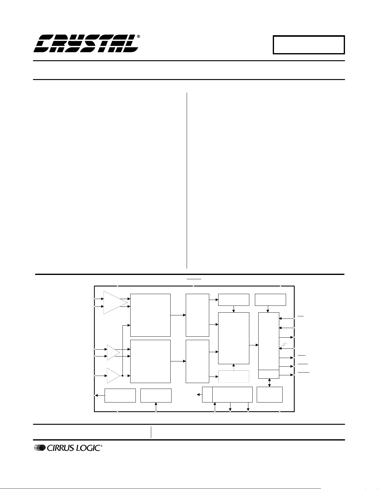
The CS5460 is a h ighly integrated ∆Σ Analog-to -Digital
Converter (ADC) which combines two ∆Σ ADCs, high
speed power calculation functions, and a serial interface
on a single chip. It is desi gned to accurately measure
and calculate: Energ y, Instantaneous Power, I
for single phase 2 or 3-wire po wer meter a pplica-
V
RMS
tions. The CS5460 interfaces to a low cost shunt or
transformer to measure c urrent, and r esistive divid er or
transformer to measure voltage. The CS5460 features a
bi-directional serial interface for communication with a
micro-controller and a fixed-width programmable frequency output that is proportional to energy. The product
is initialized and ful ly functional upon power-u p, and includes facilities for system-level calibration under control
of the user program.
ORDERING INFORMATION:
CS5460-BS -40°C to +85°C 24-pin SSOP
RMS
, and
VA+ VD+
IIN+
IIN-
VIN+
VIN-
VREFIN
VREFOUT
PGA
x10,x50
x10
x1
Voltage
Reference
VA-
4 Order
Modulator
2 Order
Modulator
Preliminary Product Information
P.O. Box 17847, Austin, Texas 78760
(512) 445 7222 FAX: (512) 445 7581
http://www.cirrus.com
RESET
Watch Dog
Timer
Serial
Interface
E-to-F
Calibration
SRAM
DGND
th
∆Σ
nd
∆Σ
Power
Monitor
PFMON
System
Clock
Digital
Filter
Digital
Filter
/K
High Pass
Calculation
I ,V )
RMS RMS
High Pass
Generator
XIN
XOUT
Filter
Power
Engine
(Energy
I * V
Filter
Clock
CPUCLK
This document contains information for a new product.
Cirrus Logic reserves the right to modify this product without notice.
Copyright Cirrus Logic, Inc. 2000
(All Rights Reserved)
CS
SDI
SDO
SCLK
INT
EDIR
EOUT
JUL ‘00
DS279PP6
1

TABLE OF CONTENTS
1. CHARACTERISTICS AND SPECIFICATIONS............................. ...... ....... ...... ....... ..... 4
ANALOG CHARACTERISTICS ...............................................................................4
5 V DIGITAL CHARACTERISTICS ......................................................................... 5
3 V DIGITAL CHARACTERISTICS ......................................................................... 6
ABSOLUTE MAXIMUM RATINGS ..........................................................................6
SWITCHING CHARACTERISTICS ... ....... ...... ............................................. ....... ..... 7
2. GENERAL DESCRIPTION ........................................................................................... 9
2.1 Theory of Operation........................................................................................... 9
2.2 Performing Measurements ................................................................................9
2.2.1 Single Computation Cycle (C = 0).......................................................... 11
2.2.2 Multiple Computation Cycles (C = 1)......................................................11
2.3 High Rate Digital Filters...................................................................................11
2.4 Pulse-Rate Output ...........................................................................................12
3. SERIAL PORT OVERVIEW........................................................................................15
3.1 Command Word (Write Only) ..........................................................................16
3.1.1 Start Conversions...................................................................................16
3.1.2 SYNC0 Command..................................................................................16
3.1.3 SYNC1 Command..................................................................................16
3.1.4 Power-up/Halt Control............................................................................ 16
3.1.5 Power-down Control...............................................................................17
3.1.6 Calibration Control .................................................................................17
3.1.7 Register Read/Write Command ............................................................. 18
3.2 Serial Port Interface.........................................................................................19
3.3 Serial Port Initialization....................................................................................19
3.4 System Initialization......................................................................................... 21
CS5460
4. REGISTER DESCRIPTION ........................... ...... ...... ....... .......................................... 2 2
4.1 Configuration Register ....................................................................................22
4.2 Current Offset Register and Voltage Offset Register ...................................... 23
4.3 Current Gain Register and Voltage Gain Register .......................................... 24
4.4 Cycle Count Register ...................................................................................... 24
4.5 Pulse-Rate Register ........................................................................................24
4.6 I,V,P,E Signed Output Register Results .........................................................24
4.7 IRMS, VRMS Unsigned Output Register Results ...........................................25
4.8 Timebase Calibration ...................................................................................... 25
4.9 Status Register and Mask Register ................................................................25
Contacting Cirrus Logic Support
For a complete listing of Direct Sales, Distributor, and Sales Representative contacts, visit the Cirrus Logic web site at:
http://www.cirrus.com/corporate/contacts/
Microwire is a trademark of National Semiconductor Corporation.
Preliminary product inf o rmation describes products whi ch are in production, but f or wh i ch ful l characterization data is not yet available. Advance produ ct i nf or -
mation describes products which are in development and subject to development changes. Cirrus Logic, Inc. has made best efforts to ensure that the information
contained in this document i s accurat e and reli able. However , t he infor mation is subje ct to chang e without noti ce and is provi d ed “AS IS” without warrant y of
any kind (express or implied). No responsibility is assumed by Cirrus Logic, Inc. for the use of this information, nor for infringements of patents or other ri g ht s
of third parties. This document is the pro perty of Cirrus Logi c, Inc. and i mplie s no licen se under patents, copyrights, tr ademarks, or trade secre ts. No part of
this publication may be copied, reproduced , stored in a retrieval system, or transmitted, in any form or by any means (electronic, mechanical, photographic, or
otherwise) without the pr i or writ ten consent of Cirrus Logic, Inc. Ite ms f rom any Ci rrus L ogi c websi t e or disk may be printed for use by the user. However, no
part of the printout or electronic files may be copied, reproduced, stored in a retrieval system, or transmitted, in any form or by any means (electronic, mechanical,
photographic, or otherwise) without the prior written consent of Cirrus Logic, Inc. Furthermore, no part of this publication ma y be used as a basis for manufacture
or sale of any items without the prior written consent of Cirrus Logic, Inc. The names of products of Cirrus Logic, Inc. or other vendors and suppliers appearing
in this document may be trademarks or service marks of their respective owners which may be registered in some jurisdictions. A list of Cirrus Logic, Inc. trademarks and service marks can be found at http://www.cirrus.com.
2 DS279PP6

CS5460
5. FUNCTIONAL DESCRIPTION ................................................................................... 28
5.1 Interrupt and Watchdog Timer......................................................................... 28
5.1.1 Interrupt.................................................................................................. 28
5.1.1.1 Clearing the Status Register ........................................................ 28
5.1.1.2 Typical use of the INT pin............................................................. 28
5.1.1.3 INT Active State ........................................................................... 28
5.1.1.4 Exceptions.................................................................................... 28
5.1.2 Watch Dog Timer................................................................................... 28
5.2 Oscillator Characteristics................................................................................. 29
5.3 Analog Inputs .................................................................................................. 29
5.4 Voltage Reference........................................................................................... 30
5.5 Performing Calibrations................................................................................... 30
5.5.1 System Calibration................................................................................. 30
5.5.2 Calibration Tips...................................................................................... 31
5.6 Phase Compensation ...................................................................................... 31
5.7 Input Current Protection.................................................................................. 31
5.8 PCB Layout ..................................................................................................... 32
6. PIN DESCRIPTION.................................................... ....... ...... ....... ...... ....... ................ 33
7. SPECIFICATION DEFINITIONS................................................................................. 34
8. PACKAGE DIMENSIONS .......................................................................................... 35
LIST OF FIGURES
Figure 1. SDI Write Timing (Not to Scale).......................................................................................8
Figure 2. SDO Read Timing (Not to Scale)..................................................................................... 8
Figure 3. Typical Connection Diagram (One-Phase 2-Wire)......................................................... 10
Figure 4. Typical Connection Diagram (One-Phase 3-Wire)......................................................... 10
Figure 5. Data Flow....................................................................................................................... 11
Figure 6. Voltage Input Filter Roll-off ............................................................................................ 12
Figure 7. Current Input Filter Roll-off............................................................................................. 12
Figure 8. Multi-Phase System....................................................................................................... 14
Figure 9. CS5460 Register Diagram............................................................................................. 15
Figure 10. Command and Data Word Timing ............................................................................... 20
Figure 11. Oscillator Connection................................................................................................... 29
Figure 12. System Calibration of Offset........................................................................................ 30
Figure 13. System Calibration of Gain.......................................................................................... 30
LIST OF TABLES
Table 1. Specification with MCLK = 4.096 MHz, K = 1, and N = 4000............................................ 9
Table 2. Internal Registers Default Value ..................................................................................... 21
Table 3. CPU Clock (and K) Restrictions...................................................................................... 29
DS279PP6 3
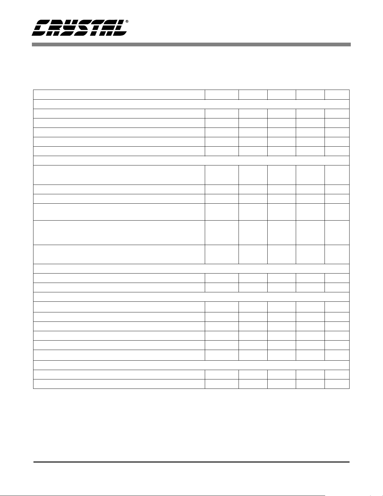
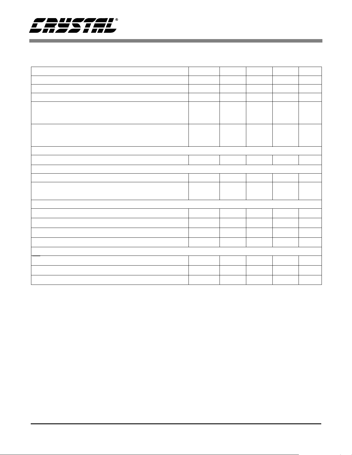
1. CHARACTERISTICS AND SPECIFICATIONS
CS5460
ANALOG CHARACTERISTICS (T
VA- = AGND; MCLK = 4.096 MHz, K = 1; N = 4000, OWR = 4.0 kHz.)(See Notes 1, 2, and 3)
Parameter Symbol Min Typ Max Unit
= -40 °C to +85 °C; VA+, VD+ = +5 V ±10%; VREFIN = 2.5 V;
A
Accuracy (Both Channels)
Total Harmonic Distortion THD 74 - - dB
Common Mode Rejection (DC, 50, 60 Hz) CMRR 80 - - dB
Offset Drift (Without the High Pass Filter) - 5 - nV/°C
Full Scale DC Calibration Range (Note 4) FSCR 25 - 100 %F.S.
Input Sampling Rate DCLK = MCLK/K - DCLK/4 - Hz
Analog Inputs (Current Channel)
Differential Input Voltage Range {(IIN+) - (IIN-)} (Gain = 10)
(Gain = 50)
Common Mode + Signal on IIN+ or IIN- (Gain = 10 or 50) -0.25 - VA+ V
Crosstalk with Voltage Channel at Full Scale (50, 60 Hz) - - -115 dB
Input Capacitance (Gain = 10)
(Gain = 50)
Effective Input Impedance (Note 5)
(Gain = 10)
(Gain = 50)
Noise (Referred to Input) (Gain = 10)
(Gain = 50)
IIN 0
IC -
EII
30
30
-
0
-
-
-
-
5
25
-
-
-
-
±250
±50
-
-
-
-
20
4
mV(dc)
mV(dc)
pF
pF
kΩ
kΩ
µV
rms
µV
rms
Accuracy (Current Channel)
Bipolar Offset Error (Note 1) VOS - - ±0.001 %F.S.
Full-Scale Error (Note 1) FSE - - ±0.001 %F.S.
Analog Inputs (Voltage Channel)
Differential Input Voltage Range {(VIN+) - (VIN-)} VIN 0 - ±250 mV(dc)
Common Mode + Signal on VIN+ or VIN- -0.25 - VA+ V
Crosstalk with Current Channel at Full Scale (50, 60 Hz) - - -70 dB
Input Capacitance IC - 0.2 - pF
Effective Input Impedance (Note 5) EII 5 - - MΩ
Noise (Referred to Input) - - 250 µV
rms
Accuracy (Voltage Channel)
Bipolar Offset Error (Note 1) VOS - - ±0.01 %F.S.
Full-Scale Error (Note 1) FSE - - ±0.01 %F.S.
Notes: 1. Applies after system calibration
2. Specifications guaranteed by design, characterization, and/or test.
3. Analog signals are relative to VA- and digital signals to DGND unless otherwise noted.
4. The minimum FSCR is limited by the maximum allowed gain register value.
5. Effective Input Impedance (EII) varies with clock frequency (DCLK) and Input Capacitance (IC)
EII = 1/(IC*DCLK/4)
4 DS279PP6
CS5460
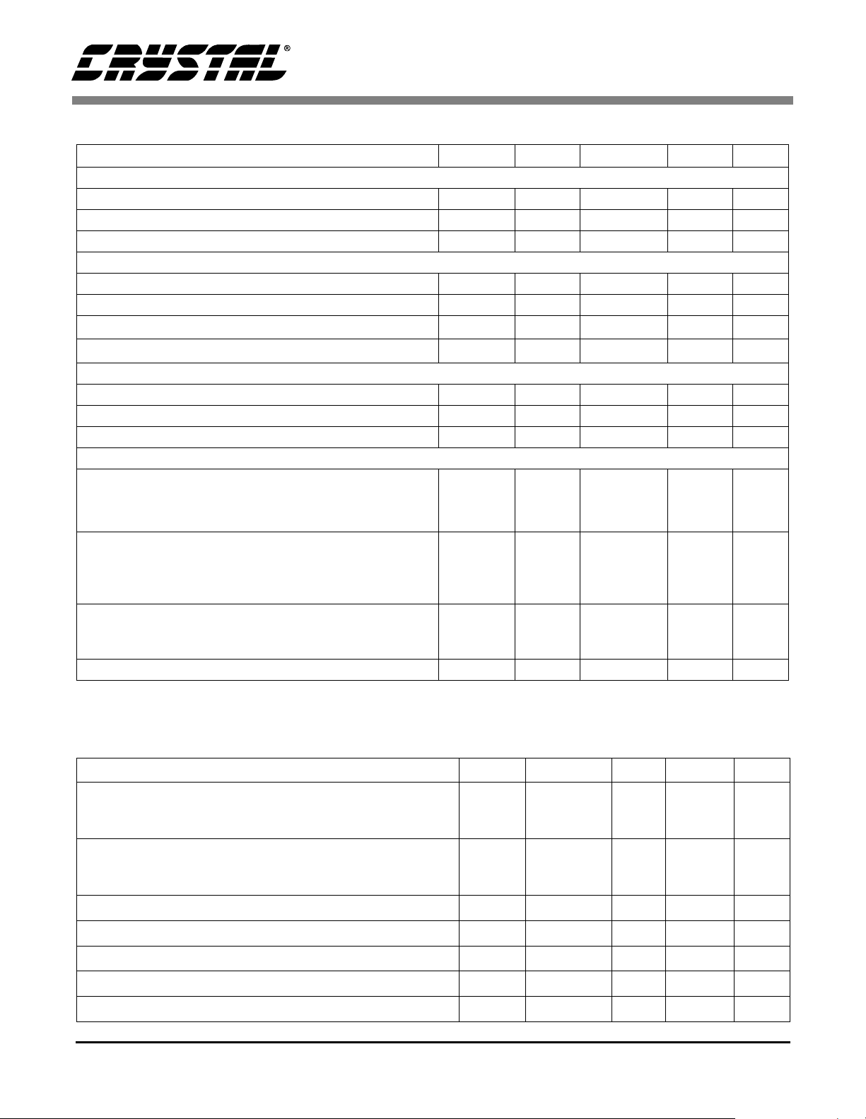
ANALOG CHARACTERISTICS (Continued)
Parameter Symbol Min Typ Max Unit
Dynamic Characteristics
Phase Compensation (Voltage Channel at 60 Hz) -2.4 - +2.5 °
High Rate Filter Output Word Rate (Both Channels) OWR - DCLK/1024 - Hz
High Pass Filter Pole Frequency -3 dB - 0.5 - Hz
Reference Output
Output Voltage REFOUT 2.4 - 2.6 V
Temperature Coefficient - 25 60 ppm/°C
Load Regulation (Output Current 1 µA Source or Sink) ∆V
R
Output Noise Voltage (0.1 Hz to 512 kHz) eN - 100 - µV
Reference Input
Input Voltage Range VREFIN 2.4 2.5 2.6 V
Input Capacitance - 4 - pF
Input CVF Current - 25 - nA
Power Supplies
Power Supply Currents (Normal Mode) I
I
(VD+ = 5 V)
D+
(VD+ = 3 V)
I
D+
Power Consumption Normal Mode (VD+ = 5 V)
A+
PSCA
PSCD
PSCD
PC -
(Note 6) Normal Mode (VD+ = 3 V)
Standby
Sleep
Power Supply Rejection (50, 60 Hz)
(Gain = 10)
(Gain = 50)
PSRR
PSRR
Power Monitor Thresholds PM 2.3 2.7 V
-610mV
rms
-
-
-
-
-
-
1.3
2.9
1.7
21
11.6
6.75
10
25
-
-
-
mA
mA
mA
mW
-
-
-
mW
mW
µW
-56
70
dB
dB
Notes: 6. All outputs unloaded. All inputs CMOS level.
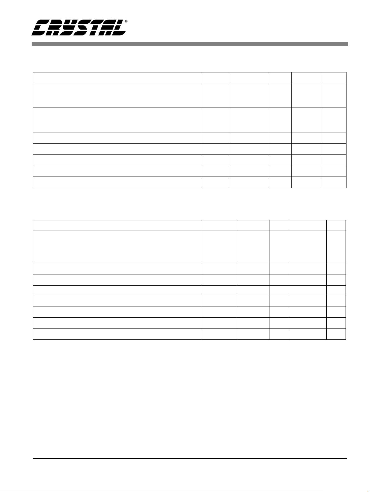
5 V DIGITAL CHARACTERISTICS (T
= -40 °C to +85 °C; VA+, VD+ = 5 V ±10% VA-, DGND = 0
A
V) (See Notes 2 and 7)
Parameter Symbol Min Typ Max Unit
High-Level Input Voltage All Pins Except XIN and SCLK
XIN
SCLK
Low-Level Input Voltage All Pins Except XIN and SCLK
XIN
SCLK
High-Level Output Voltage I
Low-Level Output Voltage I
= +5 mA V
out
= -5 mA V
out
Input Leakage Current I
3-State Leakage Current I
Digital Output Pin Capacitance C
V
V
OH
OL
in
OZ
out
IH
0.6 VD+
(VD+) - 0.5
0.8 VD+
IL
-
-
-
(VD+) - 1.0 - - V
--0.4V
-±1±10µA
--±10µA
-5-pF
-
-
-
-
-
-
-
-
-
0.8
1.5
0.2 VD+
V
V
V
V
DS279PP6 5
CS5460
3 V DIGITAL CHARACTERISTICS (T
= -40 °C to +85 °C; VA+ = 5 V ±10%, VD+ = 3 V ±10%; VA-,
A
DGND = 0 V) (See Notes 2 and 7)
Parameter Symbol Min Typ Max Unit
High-Level Input Voltage All Pins Except XIN and SCLK
XIN
SCLK
Low-Level Input Voltage All Pins Except XIN and SCLK
XIN
SCLK
High-Level Output Voltage I
Low-Level Output Voltage I
= +5 mA V
out
= -5 mA V
out
Input Leakage Current I
3-State Leakage Current I
Digital Output Pin Capacitance C
V
V
OH
OL
in
OZ
out
IH
IL
0.6 VD+
(VD+) - 0.5
0.8 VD+
-
-
-
-
-
-
-
-
-
(VD+) - 1.0 - - V
--0.4V
-±1±10µA
--±10µA
-5-pF
-
-
-
0.48
0.3
0.2 VD+
V
V
V
V
Notes: 7. All measurements performed under static conditions.
ABSOLUTE MAXIMUM RATINGS (DGND = 0 V; See Note 8)
Parameter Symbol Min Typ Max Unit
DC Power Supplies (Notes 9 and 10)
Positive Digital
Positive Analog
Negative Analog
Input Current, Any Pin Except Supplies (Note 11 and 12) I
Output Current I
Power Dissipation (Note 13) PDN - - 500 mW
Analog Inpu t Voltage All Analog Pins V
Digital Input Voltage All Digital Pins V
Ambient Operating Temperature T
Storage Temperature T
VD+
VA+
VA-
IN
OUT
INA
IND
A
stg
-0.3
-0.3
+0.3
-
-
-
+6.0
+6.0
-6.0
--±10mA
--±25mA
- 0.3 - (VA+) + 0.3 V
-0.3 - (VD+) + 0.3 V
-40 - 85 °C
-65 - 150 °C
V
V
V
Notes: 8. All voltages with respect to ground.
9. VA+ and VA- must satisfy {(VA+) - (VA-)} < +6.0 V.
10. VD+ and VA- must satisfy {(VD+) - (VA-)} < +6.0 V.
11. Applies to all pins including continuous over-voltage conditions at the analog input (AIN) pins.
12. Transient current of up to 100 mA will not cause SCR latch-up. Maximum input current for a power
supply pin is ±50 mA.
13. Total power dissipation, including all input currents and output currents.
WARNING: Operation at or beyond these limits may result in permanent damage to the device.
Normal operation is not guaranteed at these extremes.
6 DS279PP6
CS5460
SWITCHING CHARACTERISTICS (T
= -40 °C to +85 °C; VA+ = 5.0 V ±10%; VD+ = 3.0 V ±10%
A
or 5.0 V ±10%; VA- = 0.0 V; Logic Levels: Logic 0 = 0.0 V, Logic 1 = VD+; CL = 50pF))
Parameter Symbol Min Typ Max Unit
Master Clock Frequency Internal Gate Oscillator (Note 14) MCLK 2.5 4.096 20 MHz
Master Clock Duty Cycle 40 - 60 %
CPUCLK Duty Cycle (Note 15) 40 60 %
Rise Times Any Digital Input Except SCLK (Note 16)
SCLK
Any Digital Output
Fall Times Any Digital Input Except SCLK (Note 16)
SCLK
Any Digital Output
t
t
rise
fall
-
-
-
-
-
-
50
50
-
-
-
-
1.0
100
-
1.0
100
-
µs
µs
ns
µs
µs
ns
Start-up
Oscillator Start-up Time XTAL = 4.096 MHz (Note 17) t
ost
-60-ms
Serial Port Timing
Serial Clock Frequency SCLK - - 2 MHz
Serial Clock Pulse Width High
Pulse Width Low
t
1
t
2
200
200
-
-
-
-
ns
ns
SDI Write Timing
CS Enable to Valid Latch Clock t
Data Set-up Time Prior to SCLK Rising t
Data Hold Time After SCLK Rising t
SCLK Falling Prior to CS
Disable t
3
4
5
6
50 - - ns
50 - - ns
100 - - ns
100 - - ns
SDO Read Timing
CS Enable to Valid Latch Clock t
SCLK Falling to New Data Bit t
Rising to SDO Hi-Z t
CS
7
8
9
--150ns
--150ns
--150ns
Notes: 14. Device parameters are specified with a 4.096 MHz clock, however, clocks between 3MHz to 20 MHz
can be used.
15. If external MCLK is used, then its duty cycle must be between 45% and 55% to maintain this spec.
16. Specified using 10% and 90% points on wave-form of interest. Output loaded with 50 pF.
17. Oscillator start-up time varies with crystal parameters. This specification does not apply when using an
external clock source.
DS279PP6 7
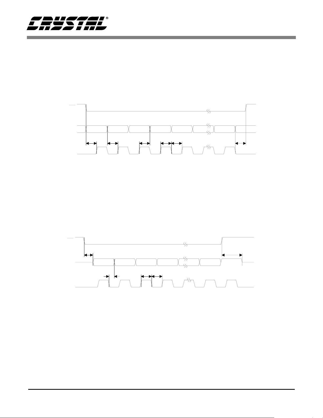
CS
CS5460
SDI
SCLK
CS
SDO
SCLK
MSB MSB - 1
t
3
t
7
t
MSB MSB - 1
t
8
t
t
4
5
t
2
1
Figure 1. SDI Write Timing (Not to Scale)
t
t
2
1
LSB
LSB
t
6
t
9
Figure 2. SDO Read Timing (Not to Scale)
8 DS279PP6

CS5460
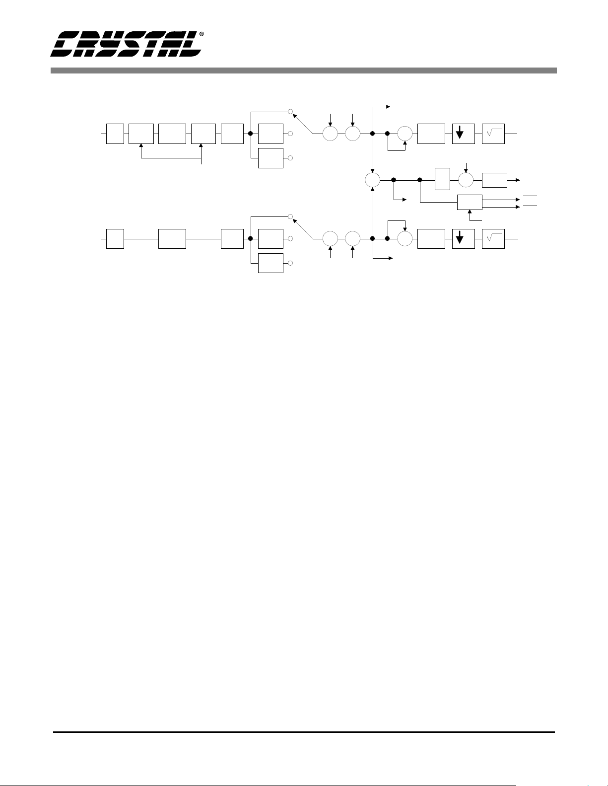
2. GENERAL DESCRIPTION
The CS5460 is a CMOS monolithic power measurement device with an energy computation engine. The CS5460 combines a programmable gain
amplifier, two ∆Σ modulators, two high rate filters,
system calibration, and power calculation functions to compute Energy, V
RMS
, I
, and Instan-
RMS
taneous Power.
The CS5460 is designed for power meter applica-
tions and is optimized to interface to shunts or current transformers to measure current, and a
resistive divider or transformer to measure voltage.
To accommodate various input voltage levels due
to shunts, the current channel includes a programmable gain amplifier (PGA) which allows the user
to measure either 150 mV
or 30 mV
RMS
RMS
sig-
nals.
The CS5460 includes two high-rate digital filters
which output data at a (MCLK/K)/1024 output word
rate (OWR). A high-pass filter in both channels can
be enabled to remove the DC content from the input
signal before the energy calculations are made.
To ease communication between the CS5460 and a
micro-controller, the converter includes a simple
three-wire serial interface which is SPI™ and Microwire™ compatible. The serial port also contains
a Schmitt Trigger input on its serial clock (SCLK)
to allow for slow rise time signals.
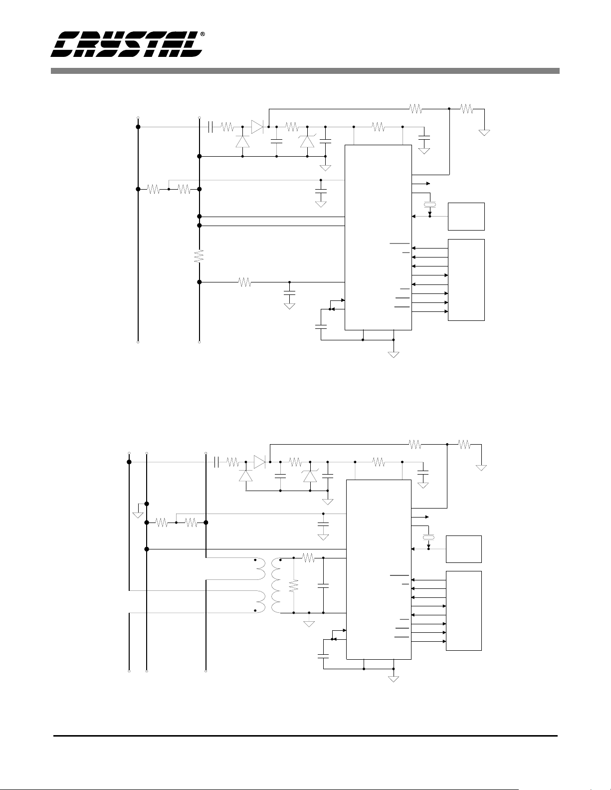
2.1 Theory of Operation
The CS5460 is designed to operate from a single
+5 V supply or dual ±2.5 V supplies, to provide a
30mV
channel and to provide a 150 mV
voltage channel. With single supply, the CS5460 is
designed to accommodate common mode signals
of -0.25 V to VA+.
Figure 3 illustrates the CS5460 connected to a service to measure power in a single-phase 2-wire system while operating in a single supply
configuration. Figure 4 illustrates the CS5460 con-
or 150 mV
RMS
range for the current
RMS
range for the
RMS
figured to measure power in a single-phase 3-wire
system.
2.2 Performing Measurements
The CS5460 performs measurements of instantaneous current, instantaneous voltage, instantaneous
power, energy, RMS current, and RMS voltage.
These measurements are output as 24-bit signed
and unsigned data formats as a percentage of full
scale. The flow of data to per form these calculations is shown in Figure 5. All of these measurements begin when a start conversion command is
given. The energy and RMS registers are then updated every N conversions (or 1 computation cycle) where N is the content of the Cycle Count
register. After the computation cycle has finished,
the DRDY bit in the Status and Mask register is set.
The INT pin will also become active if the DRDY
bit is unmasked.
Table 1 provides an example detailing the output
linearity. A computation cycle is derived from the
master clock and its frequency is
(MCLK/K)/(1024*N). Instantaneous calculations
are performed at a 4000 Hz rate where as, I
V
, and energy, are performed at a 1 Hz rate.
RMS
Also, DRDY is set only after computation cycles
are complete (i.e. there is no indicator flag to indicate when the instantaneous conversions are read;
however, if the Cycle Count register were set to 1,
all output calculations would be instantaneous and
DRDY would indicate when instantaneous calculations were finished).
Energy Vrms Irms
Range
Max Input
Linearity
(After
Calibration)
Output word
Table 1. Specificati o n wi t h MC LK = 4.0 9 6 MH z, K = 1 ,
1000:1 2:1 500:1
See
Analog Characteristics
0.1% of
reading
and N = 4000.
0.1% of
reading
24-bits
RMS
0.1% of
reading
,
DS279PP6 9
N
R
2
To Service
CS5460
5k
Ω
L
470 nF
500
Ω
500
Ω
0.1 µF100 µF
Ω
10
0.1 µF
14
3
VA+ VD+
CS5460
17
9
VIN+
*
CP
V
R
1
10
VIN-
15
IIN-
R
S
*
RP
I
CP
0.1 µF
16
12
11
IIN+
VREFIN
VREFOUT
*
I
VA- DGND
PFMON
CPUCLK
XOUT
XIN
RESET
CS
SDI
SDO
SCLK
INT
EDIR
EOUT
2
1
24
19
7
23
6
5
20
22
21
13 4
* Refer to Input Current Protection
2.5 MHz to
20 MHz
10 k
Ω
Optional
Clock
Source
Serial
Data
Interface
Figure 3. Typical Connection Diagram (One-Phase 2-Wire)
5k
Ω
N
L
1
R
1
To Service
L
2
R
2
Ω
500
470 nF
* Refer to Input Current Protection
500
Ω
R
RP
S
0.1 µF
Ω
10
XIN
CS
SDI
SDO
INT
EDIR
0.1 µF
3
17
2
1
24
19
7
23
6
5
20
22
21
0.1 µF100 µF
14
VA+ VD+
CS5460
VA-
13 4
PFMON
CPUCLK
XOUT
RESET
SCLK
EOUT
DGND
9
VIN+
*
CP
V
10
VIN-
16
CP
*
I
15
12
11
IIN+
IIN-
VREFIN
VREFOUT
*
I
2.5 MHz to
20 MHz
Interface
10 k
Ω
Optional
Clock
Source
Serial
Data
Figure 4. Typical Connection Diagram (One-Phase 3-Wire)
10 DS279PP6
V *
off
V *
gn
CS5460
V*
VOLTAGE
CURRENT
∆Σ
∆Σ
DELAY
REG
SINC
SINC
DELAY
2
REG
Config uration R egiste r *
PC[3:0] Bits
4
FIR
FIR
HPF
APF
HPF
APF
Figure 5. Data Flow.
2.2.1 Single Computation Cycle (C = 0)
Based on the information provided in the Cycle
Count register, a single computation cycle is performed after the user transmits the single conversion cycle command. After the computations are
complete, DRDY is set. Thirty-two SCLKs are
then needed to acquire a calculation result. The first
8 SCLKs are used to clock in the command to determine which result register is to be read. The last
24 SCLKs are needed to read the desired calculation result register. After reading the data, the serial
port returns to the command mode, where it waits
for a new command to be issued.
2.2.2 Multiple Computation Cycles (C = 1)
Based on the information provided in the Cycle
Count register, continuous computation cycles are
repeatedly performed on the voltage and current
cycles. Computation cycles cannot be started/stopped on a per channel basis. After each computation cycle is completed, DRDY is set.
Thirty-two SCLKs are then needed to read a register. The first 8 SCLKs are used to clock in the command to determine which results register is to be
read. The last 24 SCLKs ar e needed to re ad the calculation result. While in this mode, the user may
V *
RMS
E *
E
out
E
dir
I *
RMS
I *
off
N
+
x
x x
x
+
I *
gn
x
x
I *
* DENOTES REGISTER NAME
2
SINC
TBC *
N
Σ
P *
2
SINC
E to F
N
÷
4096
PULSE-RATE*
choose to acquire only the calculations required for
the application as DRDY rises and falls to indicate
the availability of a new data.
The RMS calculations require a Sinc2 operation
prior to their square root operation. Therefore, the
first output for each channel will be invalid (i.e. all
RMS calculations are invalid in the single computation cycle routine and the first RMS calculations
will be invalid in the continuous computation cycle). All energy calculations will be valid since en-
ergy calculations don’t require this Sinc2 operation.
2.3 High Rate Digital Filters
The high rate filter on the voltage channel is imp lemented as a fixed sinc2 filter, compensated by a
short length FIR. When the converter is driven with
a 4.096 MHz clock (K=1), the filter has a magnitude response similar to that shown in Figure 6.
Note that the filter’s response scales with MCLK
frequency and K.
The current channel contains a sinc4 filter, com pensated by a short length FIR. When the converter is
driven with a 4.096 MHz clock (K=1) the composite filter response is given in Figure 7.
DS279PP6 11

CS5460
Figure 6. Voltage Input Filter Roll-off
-2.5
-2
-1.5
-1
-0.5
0
0.5
0 200 400 600 800 1000 1200 1400 1600 1800 2000
Gain (dB)
Frequenc y (Hertz)
Figure 7. Current Input Filter Roll-off
0.5
0.0
-0.5
-1.0
Gain (dB)
-1.5
-2.0
-2.5
0 200 400 600 800 1000 1200 1400 1600 1800 2000
Frequency (Hertz)
15 A respectively, noting that the maximum rated
levels on the power line are 250 V and 20 A. We
also assume that we have calibrated the CS5460
voltage/current channel inputs such that a DC voltage level of 250 mV wi ll cause full -scale readings
of 1.0 in the CS5460A Instantaneous Voltage and
Current Registers as well as in the RMS-Voltage
and RMS-Current Registers. We want to find out
what frequency value we should put into the
CS5460’s pulse-rate register (call this value ‘PR’)
in order to satisfy this re quirement. Our first step is
to set the voltage and current sensor gain constants,
KV and KI, such that there will be acceptable input
voltage levels on the inputs when the power line
voltage and current levels are at the maximum values of 250 V and 20 A, respectively. We need to
calculate KV and KI in order to determine the appropriate ratios of the voltage/current transformers
and/or shunt resistor values to use in the front-end
voltage/current sensor networks.
We assume here that we are dealing with a sinusoidal AC power signal. For a sinewave, the la rgest
RMS value that can be accurately measured (without over-driving the inputs) will register at ~0.7071
of the maximum DC input level. Since power signals are often not perfectly sinusoidal in real-world
situations, and to provide for some over-range capability, we will set the RMS-Voltage and
2.4 Pulse-Rate Output
As an alternative to reading the energy through the
serial port, the EOUT and EDIR pins provide a
simple interface with which signed energy can be
accumulated. Each EOUT pulse represents a predetermined magnitude of energy. The accompanying
EDIR level represents the sign of the energy. With
MCLK = 4.096 MHz, K = 1, and both ADC inputs
at their maximum DC values, the pulses will have
a frequency equal to that in the pulse rate register.
EXAMPLE #1: Suppose that we want the
pulse-frequency on the EOUT pin to be ‘IR’ = 100
pulses per second (100 Hz) when the RMS-voltage/-current levels on the power line are 220 V and
RMS-Current Registers to measure at 0.6 when the
RMS-values of the line-voltage and line-current
levels are at 250 V and 20 A. Therefore, when the
RMS registers measure 0.6, the voltage level at the
inputs will be 0.6 x 250 mV = 150 mV. We now
find our sensor gain constants, KV and KI, by demanding that the voltage and current channel inputs should be at 150 mV RMS when the power
line voltage and current are at the maximum va lues
of 250 V and 20 A.
KV = 150 mV / 250 V = 0.0006
KI = 150 mV / 20 A = 0.0075 Ohms
These sensor gain constants can help determine the
12 DS279PP6

CS5460
PulseRate IR PR
V
Vnom
250 m V
------------------
V
Inom
250mV
------------------
⋅⋅==
PR
IR
V
Vnom
250 m V
------------------
V
Inom
250 m V
------------------
×
------------------------------------------- -
100 H z
132mV
250mV
------------------
112.5 mV
250 m V
-----------------------
×
------------------------------------------------
==
PR
IR
V
Vnom
250 m V
------------------
V
Inom
50mV
---------------
×
---------------------------------------- -
=
ratios of the transformer or resistor-divider sensor
networks. We now use these sensor gain constants
to calculate what the input voltage levels will be on
the CS5460 inputs when the line-voltage and
line-current are at 220 V and 15 A. We call these
values VVnom and VInom.
VVnom = KV * 220 V = 132 mV
VInom = KI * 15 A = 112.5 mV
The pulse rate on EOUT will be at ‘PR’ pulses per
second (Hz) when the RMS-levels of voltage/current inputs are at 250 mV. When the voltage/current inputs are set at VVnom and VInom, we want the
pulse rate to be at ‘IR’ = 100 pulses per second. IR
will be some percentage of PR. The percentage is
defined by the ratios of VVnom/250 mV and
VInom/250 mV with the following formula:
We can rearrange the above equation and solve for
PR. This is the value that we put into the pul se-rate
register.
EXAMPLE #2: Suppose that instead of being given a desired frequency of pulses per second to be issued at a specific voltage/current level, we are
given a desired number of pulses per unit energy to
be present at EOUT, given that the maximum
line-voltage is at 250 V (RMS) and the maximum
line-current is at 20 A (RMS). For example, suppose that the required number of pulses per kW-hr
is specified to be 500 pulses/kW-hr. In such a situation, the nominal line voltage and current do not
determine the appropriate pulse-rate setting. Instead, the maximum line-voltage and line-current
levels must be considered. We use the given maximum line-voltage and line-current levels to determine KV and KI as previously described to get:
KV = 150 mV / 250 V = 0.0006
KI = 150 mV / 20 A = 0.0075 Ohms
where we again have calculated our sensor gains
such that the maximum line-voltage and line-current levels will measure as 0.6 in the RMS-voltage
and RMS-current registers.
We can now calculate the required Pulse-Rate Register setting by using the following equation:
Therefore we set the Pulse-Rate Register to
~420.875 Hz. Therefore, the Pulse-Rate Register
would be set to 0x00349C.
The above equation is valid when current channel
is set to x10 gain. If current channel gain is set to
x50, then the equation becomes:
where it is assumed that the current channel has
been calibrated such th at the current-register will
read at full-scale when the input voltage across the
IIN+ and IIN- inputs is 50 mV (DC).
DS279PP6 13
PR 500
pulses
-----------------kW hr⋅
1hr
--------------
⋅⋅ ⋅ ⋅=
3600 s
1kW
------------ ----- 1000W
250mV
------------------
250m V
------------------
K
K
V
I
Therefore PR = ~1.929 Hz.
Note that the Pulse-Rate Register cannot be set to a
frequency of exactly 1.929 Hz. The closest setting
that the Pulse-Rate register can obtain is 0x00003E
= 1.9375. To improve the accuracy, either gain register can be programmed to correct for the
round-off error in PR. This value would be calculated as
PR
Ign or Vgn
-------------
1.00441≅ 0 x404830==
1.929
To allow for a simpler interface in a multi-phase
system, the EOUT and EDIR pins can be connected
together and used in a wired-or configuration. The
parts must be driven with the same clock and pro-

grammed with different phases (PH[1:0] in the
Phase - 00
Phase - 01
Phase - 10
Phase - 11
t
≅
Pulse-Rate Register Period
8
N
MCLK/K
=
for Integer N
t
t
Figure 8. Multi-Phase System
Configuration register). The pulse width and the
pulse separation is an integer multiple of system
clocks (approximately equal to 1/8 of the period of
the contents of the pulse-rate register). The maximum frequency is therefore MCLK/K/8. A timing
diagram for a multi-phase system is shown in
Figure 8.
CS5460
14 DS279PP6

CS5460
3. SERIAL PORT OVERVIEW
The CS5460’s serial port incorporates a state machine with transmit/re ceive buffers. The state machine interprets 8 bit command words on the rising
edge of SCLK. Upon decoding of the command
word the state machine performs the requested
command or prepares for a data transfer of the a ddressed register. Request for a rea d requires an internal register transfer to the transmit buffer, while
a write waits until the completion of 24 SCLKs before performing a transfer. The internal registers
are used to control the ADC’s functions. All registers are 24-bits in length. Figure 9 depicts the internal registers available to the user.
After system initialization or reset, the serial port
state machine is initialized into command mode
where it waits to receive a valid command (the first
8-bits clocked into the serial port). Upon receiving
and decoding a valid command word the state machine instructs the converter to either perform a
system operation, or transfer data to or from an internal register. The Command Word section can be
used to decode all valid commands.
The state machine decodes the command word as it
is received. The serial port enters data transfer
mode if the MSB of the command word is logic 0
(B7 = 0). In data transfer mode, the internal registers are read from or written to. Command words
instructing a register write must be followed by 24
bits of data. For instance, to write the configuration
register, the user would transmit the command
(0x40) to initiate the write. The ADC would then
acquire the serial data input from the (SDI) pin
when the user pulses the serial clock (SCLK) 24
times. Once the data is received the state machine
would write the data to the configuration register
and return to the command mode. Command words
instructing a register read may be terminated at
8-bit boundaries (e.g., read transfers may be 8, 16,
or 24 bits in length). Also data register reads allow
“command chaining”. For example, a command
word instructs the state machine to read a signed
output register. After the user pulses SCLK for
16-bits of data, a write command word (e.g., to
clear the status register) may be pulsed on to the
SDI line at the same time the remaining 8-bits of
data are pulsed from the SDO line.
Current
Channel
Voltage
Channel
DS279PP6 15
Offset Regi ster (1 × 24)
Offset Register (1 × 24)
Pulse-Rate Register (1 × 24)
Timebase Register (1 × 24)
Configuration Regi ster (1 × 24)
Gain Regi ster (1 × 24)
Gain Reg ister (1 × 24)
Cycle-Counter Register (1 × 24)
Status Register (1 × 24)
Mask Re gister (1 × 24 )
Figure 9. CS5 460 Register Di agram
Signed Output Registers (4 × 24)
(I, V, P, E)
Unsigned Out put Registe rs (2 × 24)
(I , V )
RMS RMS
Receive Buffer
24-Bit
Seri al Interfac e
Transmit Buffer
Command Word
State Mach ine
SDI
CS
SDO
SCLK
INT

CS5460
3.1 Command Word (Write Only)
All command words are always 1 byte in length. Commands that write to a register initiate 3 bytes of register data.
Commands that read from registers must be followed by 1, 2, or 3 bytes of register read data. Commands that read
data can be chained with other commands (e.g., while reading data, a new command can be sent to SDI which can
execute before the original read is completed). This allows for “chaining” commands.
3.1.1 Start Conversions
B7 B6 B5 B4 B3 B2 B1 B0
1110C000
This command indicates to the state machine to begin acquiring measurements and calculating results. The device
has two modes of acquisition.
C Modes of measurement
0 = Perform a single computation cycle
1 = Perform continuous computation cycles
3.1.2 SYNC0 Command
B7 B6 B5 B4 B3 B2 B1 B0
11111110
This command is the end of the serial port re-initialization sequence. The command can also be used as a NOP
command. The serial port is resynchronized to byte boundaries by sending three or more consecutive SYNC1 commands followed by a SYNC0 command.
3.1.3 SYNC1 Command
B7 B6 B5 B4 B3 B2 B1 B0
11111111
This command is part of the serial port re-initialization sequence. The command can also serve as a NOP command,
but no more than three consecutive bytes should be transmitted.
3.1.4 Power-up/Halt Control
B7 B6 B5 B4 B3 B2 B1 B0
10100000
If the device is powered-down, this command will power-up the device. When powered-on, no computations will be
running. If the part is already powered-on, all computations will be halted.
16 DS279PP6

CS5460
3.1.5 Power-down Control
B7 B6 B5 B4 B3 B2 B1 B0
1 0 0S1S00 0 0
The device has two power-down modes to conserve power. If the chip is put in stand-by mode all circuitry except
the clock generator is turned off.
S1,S0 Power-down mode
00 = Reserved
01 = Halt and enter stand-by power saving mode. This mode allows quick power-on time
10 = Halt and enter sleep power saving mode. This mode requires a slow power-on time
11 = Reserved
3.1.6 Calibration Control
B7 B6 B5 B4 B3 B2 B1 B0
110CvCi0GCOC
The device has the capability of performing a system offset and gain calibration. The user must supply the proper
inputs to the device before proceeding with the calibration cycle.
Cv,Ci Designates calibrati on channel
00 = Not allowed
01 = Calibrate the current channel
10 = Calibrate the voltage channel
11 = Calibrate voltage and current channel simultaneously
GC Designates gain calibration
0 = Normal operation
1 = Perform gain calibration
OC Designates offset calibration
0 = Normal operation
1 = Perform offset calibration
DS279PP6 17

CS5460
3.1.7 Register Read/Write Command
B7 B6 B5 B4 B3 B2 B1 B0
0W/R
This command informs the state machine that a register access is required. On reads the addressed register is loaded into the output buffer and clocked out by SCLK. On writes the data is clocked into the input buffer and transferred
to the addressed register on the 24
RA4 RA3 RA2 RA1 RA0 0
th
SCLK.
W/R
Write/Read control
0 = Read register
1 = Write register
RA[4:0] Register address bits. Binary encoded 0 to 31. All registers are 24 bits in length.
Address Name Description
00000 Config Configuration Register
00001 Ioff Current offset calibration
00010 Ign Current gain calibration
00011 Voff Voltage offset calibration
00100 Vgn Voltage gain calibration
00101 Cycle Count Number of conversions to integrate over (N)
00110 Pulse-Rate Used to calibrate/scale the energy to frequency output
00111 I Last current value
01000 V Last voltage value
01001 P Last Power value
01010 E Total energy value of last cycle
01011 I
01100 V
RMS
RMS
RMS current value of last cycle
RMS voltage value of last cycle
01101 TBC Timebase Calibration
01110 Test Internal Use only †
01111 Status Status register
10000 Res Reserved
.
.
10111 Res Reserved
11000 Test Internal Use only †
11001 Test Internal Use Only †
11010 Mask Interrupt mask register
11011 Test Internal Use Only †
11100 Res Reserved
.
.
11111 Res Reserved
† These Registers are for Internal Use only and should not be written to. Accessing these
registers will NOT generate an “Invalid Command” (IC
) bit in the Status Register.
18 DS279PP6

CS5460
3.2 Serial Port Interface
The CS5460’s serial interface consists of four control lines: CS, SDI, SDO, and SCLK.
CS, Chip Select, is the control line which enables
access to the serial port. If the C S pin is tied to logic
0, the port can function as a three wire interf ace.
SDI, Serial Data In, is the data signal used to transfer data to the converters.
SDO, Serial Data Out, is the data signal used to
transfer output data from the converters. The SDO
output will be held at high impedance any time CS
is at logic 1. Figure 10 illustrates the serial sequence necessary to write to, or read from the serial
port’s buffers.
SCLK, Serial Clock, is the serial bit-clock which
controls the shifting of data to or from the ADC’s
serial port. The CS pin must be held at logic 0 before SCLK transitions can be recognized by the
port logic. To accommodate opto-isolators SCLK
is designed with a Schmitt-trigger input to allow an
opto-isolator with slower rise and fall times to directly drive the pin. Additionally, SDO is capable
of sinking or sourcing up to 5 mA to directly drive
an opto-isolator LED. SDO will have less than a
400 mV loss in the drive voltage when sinking or
sourcing 5 mA.
As shown in Figure 10 a transfer of data is always
initiated by sending the appropriate 8-bit command
(MSB first) to the serial port (SDI pin). It is impor-
tant to note that some commands use information
from the cycle-counter and configuration registers
to perform the function. For those commands it is
important that the correct information is written to
those registers first.
When a command involves a write operation the
serial port will continue to clock in the data bits
(MSB first) on the SDI pin for the next 24 SCLK
cycles. When a read command is initiated the serial
port will start transferring register content bit serial
(MSB first) on the SDO pin for the next 8, 16, or 24
SCLK cycles depending on the command issued.
The micro-controller is allowed to send a new command while reading register data. The new command will be acted upon immediately and could
possibly terminate the register read. During the
read cycle, the SYNC0 command (NOP) should be
strobed on the SDI port while clocking the data
from the SDO port.
3.3 Serial Port Initialization
The serial port is initialized to the command mode
whenever a reset is performed o r when the port initialization sequence is completed. The port initialization sequence involves clocking 3 (or more)
SYNC1 command bytes (0xFF) followed by
SYNC0 command byte (0xFE). This sequence
places the chip in the command mode where it
waits until a valid command is received.
DS279PP6 19

CS
SCLK
CS5460
CS
SCLK
SDI
SDO
SDI
MSB MSBLSB
Command Time 8 SCLKs Data Time 24 SCLKs
Write Cycle
MSB
Command Time 8 SC LKs
LSB
LSB
MSB LSB
Data Time 24 SCLKs
Read Cycle
Figure 10. Command and Data Word Timing
20 DS279PP6

3.4 System Initialization
A software or hardware reset can be initiated at any
time. The software reset is initiated by writing a
logic 1 to the RS (Reset System) bit in the configuration register, which automatically returns to logi c
0 after reset. At the end of the 32nd SCLK (i.e., 8 bit
command word and 24 bit data word) internal synchronization delays the loading of the configuration register by 3 or 4 DCLK (MCLK/K). Then the
reset circuit initiates the reset routine on the 1st falling edge of MCLK. A hardware reset is initiated
when the RESET pin is forced low with a minimum
pulse width of 50 ns. The RESET signal is asynchronous requiring no MCLKs for the part to detect
and store a reset event. Once the RESET pin is inactive the internal reset c ircuitry re mains ac tive for
5 MCLK cycles to insure resetting the synchronous
circuitry in the device. The modulators are held in
reset for 12 MCLK cycles after RES ET becomes
CS5460
in
active. The internal registers (some of which drive
output pins) will be reset to their default values on
the first MCLK re ceived after detecting a reset event
(see Table 2). After a reset, the on-chip registers are
initialized to the following states and the converter
is placed in the command mode where it waits for a
valid
command.
Configuration Registe r: 0x000001
Offset Register: 0x000000
Gain Registers 0x400000
Pulse-Rate Register: 0 x0FA000
Cycle-Counter Register: 0x000FA0
Timebase Register: 0x800000
Status Register: 0x000001
Mask Register 0x000000
Signed Registers 0x000000
Unsigned Registers 0x000000
Table 2. Internal Registers Default Value
DS279PP6 21

4. REGISTER DESCRIPTION
CS5460
Notes: * “
** “default” => bit status after reset
RA[4:0]
” => register address bits in the Register Read/Write Command word
4.1 Configuration Register
Address: RA[4:0]* = 0x00
23 22 21 20 19 18 17 16
PC3 PC2 PC1 PC0 0 0 0 Gi
15 14 13 12 11 10 9 8
EWA PH1 PH0 SI1 SI0 EOD DL1 DL0
76543210
RS VHPF IHPF iCPU K3 K2 K1 K0
Default** = 0x000001
K[3:0] Clock divider. A 4 bit binary number ranging from 0 to 15 used to divide the value of MCLK to
generate the internal clock DCLK. The internal clock frequency of DCLK = MCLK/K. Valid values are 1,2, and 4.
0001 = divide by 1 (default)
0010 = divide by 2
0100 = divide by 4
iCPU Inverts the CPUCLK clock. In order to reduce the level of noise present when analog signals
are sampled, the logic driven by CPUCLK should not be active during the sample edge.
0 = normal operation (default)
1 = minimize noise when CPUCLK is driving rising edge logic
IHPF Control the use of the High Pass Filter on the Current Channel.
0 = High-pass filter is disabled. If VHPF is set, use all-pass filter. Otherwise, no filter is used.
(default)
1 = High-pass filter is enabled.
VHPF Control the use of the High Pass Filter on the voltage Channel.
0 = High-pass filter is disabled. If IHPF is set, use all-pass filter. Otherwise, no filter is used.
(default)
1 = High-pass filter enabled
RS Start a chip reset cycle when se t 1. The re set cyc le last s for le ss than 1 0 XIN cycl es. The bit is
automatically returned to 0 by the reset cycle.
DL0 When EOD = 1, EDIR
Default = '0'
DL1 When EOD = 1, EOUT
Default = '0'
EOD Allows the EOUT
also be accessed using the status register.
0 = Normal operation of the EOUT
1 = DL0 and DL1 bits control the EOUT
becomes a user defined pin. DL0 sets the value of the EDIR pin.
becomes a user defined pin. DL1 sets the value of the EOUT pin .
and EDIR pins to be controlled by the DL0 and DL1 bits. EOUT and EDIR can
and EDIR pins. (default)
and EDIR pins.
22 DS279PP6

CS5460
SI[1:0] Soft interrupt configuration. Select the desired pin behavior for indication of an interrupt.
00 = active low level (default)
01 = active high level
10 = falling edge (INT is normally high)
11 = rising edge (INT is normally low)
PH[1:0] Set the phase of the EOUT and EDIR output pin pulse. The EOUT and EDIR pins, on different
phases, can be wire-ORed together as a simple way of summing the frequency of different
parts.
00 = phase 0 (default)
01 = phase 1
10 = phase 2
11 = phase 3
EWA Allows the output pins of EOUT and EDIR of multiple chips to be connected in a wire-AND, us-
ing an external pull-up device.
0 = normal outputs (default)
1 = only the pull-down device of the EOUT and EDIR pins are active
Gi Sets the gain of the current PGA
0 = gain is 10 (default)
1 = gain is 50
Res Reserved. These bits must be set to zero.
PC[3:0] Phase compensation. A 2’s complement number used to set the delay in the voltage channel.
The bigger the number, the greater the delay in the voltage. The phase adjustment range is
about -2.4 to +2.5 degrees at 60 Hz. Each step is about 0.34 degrees at 60 Hz.
0000 = Zero degrees phase delay (default)
4.2 Current Offset Register and Voltage Offset Register
Address: RA[4:0]* = 0x01 (Current Offset Register)
RA[4:0]* = 0x03 (Voltage Offset Register)
MSB LSB
-(20)2-12
-2
Default** = 0.000
The Offset Registers are initialized to zero on reset, allowing the device to function and perform measurements.
The register is loaded after one computation cycle with the system current or voltage offset when the proper
input is applied and the Calibration Command is received. The register may be read and stored so the register
may be restored with the desired system offset compensation. The offset range is ± full scale. Format of the
register value is two’s complement notation.
-3
2
-4
2
-5
2
-6
2
-7
2
.....
-17
2
-18
2
-19
2
-20
2
-21
2
-22
2
-23
2
DS279PP6 23

CS5460
4.3 Current Gain Register and Voltage Gain Register
Address: RA[4:0]* = 0x02 (Current Gain Register)
RA[4:0]* = 0x04 (Voltage Gain Register)
MSB LSB
1
2
4.4 Cycle Count Register
MSB LSB
23
2
0
2
-1
2
-2
2
-3
2
-4
2
-5
2
-6
2
.....
-16
2
-17
2
-18
2
-19
2
-20
2
-21
2
Default** = 1.000
The Gain Registers are initialized to 1.0 on reset, allowing the device to function and perform measurements.
The register is loaded after one cycle with the system gain when the proper input is applied and the Calibration
Command is received. The register may be read and stored so the register may be restored with the desired
system offset compensation. The value is in the range 0.0 ≤ Gain < 4.0.
Address: RA[4:0]* = 0x05
22
2
21
2
20
2
19
2
18
2
17
2
16
2
.....
6
2
5
2
4
2
3
2
2
2
1
2
Default** = 4000
-22
2
0
2
The Cycle Count Register determines the length of an energy and RMS conversion. A conversion cycle is derived from (MCLK/K)/(1024∗N) where MCLK is master clock, K is clock divider, and N is cycle count. N must be
, V
greater than 10 for I
RMS
and energy calculations to be performed.
RMS
4.5 Pulse-Rate Register
Address: RA[4:0]* = 0x06
MSB LSB
18
2
17
2
16
2
15
2
14
2
13
2
12
2
11
2
.....
1
2
0
2
-1
2
-2
2
-3
2
-4
2
Default** = 32000.00 Hz
The Pulse-Rate Register determines the frequency of the train of pulses output on the EOUT
pulse represents a predetermined magnitude of energy.The register’s smallest valid value is 2
-5
increments.
2
pin. Each EOUT
-4
but can be in
4.6 I,V,P,E Signed Output Register Results
Address: RA[4:0]* = 0x07 - 0x0A
MSB LSB
-(20)2-12
Access: Read Only
-2
-3
2
-4
2
-5
2
-6
2
-7
2
.....
-17
2
-18
2
-19
2
-20
2
-21
2
-22
2
-5
2
-23
2
The Signed Registers contain the last value of the measured results of I, V, P, and E. The results are in the
range of -1.0 ≤ I, V, P, E < 1.0. The value is represented in two's complement notation, with the binary point
place to the right of the MSB (which is the sign bit). I, V, P, and E are output results registers which contain
signed values. Note that the I, V, and P registers are updated every conversion cycle, while the E register is
only updated after each computation cycle. The numeric format of this register is two’s complement notation.
24 DS279PP6

CS5460
4.7 I
RMS
, V
Unsigned Output Register Results
RMS
Address: RA[4:0]* = 0x0B - 0x0C
MSB LSB
-1
2
-2
2
-3
2
-4
2
-5
2
-6
2
-7
2
-8
2
.....
-18
2
-19
2
-20
2
-21
2
-22
2
-23
2
Access: Read Only
The Unsigned Registers contain the last value of the calculated results of I
range of 0.0 ≤ I
left of the MSB. I
RMS,VRMS
RMS
< 1.0. The value is represented in binary notation, with the binary point place to the
and V
are output result registers which contain unsigned values.
RMS
RMS
and V
. The results are in the
RMS
4.8 Timebase Calibration
Address: RA[4:0]* = 0x0D
MSB LSB
0
2
-1
2
-2
2
-3
2
-4
2
-5
2
-6
2
-7
2
.....
-17
2
-18
2
-19
2
-20
2
-21
2
-22
2
Default** = 1.000
The Timebase Register is initialized to 1.0 on reset, allowing the device to function and perform computations.
The register is user loaded with the clock frequency error to compensate for a gain error caused by the crystal/oscillator tolerance. The value is in the range 0.0 ≤ TBC < 2.0.
-24
2
-23
2
4.9 Status Register and Mask Register
Address:
23 22 21 20 19 18 17 16
DRDY EOUT EDIR Res MATH Res IOR VOR
15 14 13 12 11 10 9 8
PWOR IROR VROR EOR EOOR Res Res Res
Res Res WDT VOD IOD LSD 0
Default** = 0x000001 (Status Register)
The Status Register indicates the condition of the chip. In normal operation writing a ’1’ to a bit will cause the bit
to go to the ’0’ state. Writing a ’0’ to a bit will maintain the status bit in its current state. With this feature the user
can simply write back the status register to clear the bits that have been seen, without concern of clearing any
newly set bits. Even if a status bit is masked to prevent the interrupt, the status bit will still be set in the status
register so the user can poll the status.
The Mask Register is used to control the activation of the INT
allow the corresponding bit in the status register to activate the INT
IC
RA[4:0]* = 0x0F
RA[4:0]* = 0x1A (Mask Register)
(Status Register)
76543210
0x000000 (Mask Register)
pin. Placing a logic ’1’ in the mask register will
pin when the status bit becomes active.
Invalid Command. Normally logic 1. Set to logic 0 when the part is given an invalid command.
Can be deactivated only by sending a port initialization sequence to the serial port. When writing
to Status Register this bit is ignored.
IC
DS279PP6 25

CS5460
LSD Low Supply Detect. Set when the voltage at the PFMON pin falls below the low-voltage thresh-
old (with respect to VA- pin). For a given part, this threshold can anywhere between 2.3 V to
2.7 V.
IOD Modulator oscillation detect on the current channel. Set when the modulator oscillates due to
an input above Full Scale. Note that the level at which the modulator oscillates is significantly
higher than the current channel’s Differential Input Voltage Range.
VOD Modulator oscillation detect on the voltage channel. Set when the modulator oscillates due to
an input above Full Scale. Note that the level at which the modulator oscillates is significantly
higher than the current channel’s Differential Input Voltage Range.
NOTE: This IOD and VOD bits may be ‘falsely’ triggered by very brief voltage spikes from the
power line. This event should not be confused with a DC overload situation at the inputs, when
the IOD and VOD bits will re-assert themselves even after being cleared, multiple times.
WDT Watch-Dog Timer. Set when there has been no reading of the Energy register for more than 5
seconds. (MCLK = 4.096 MHz, K = 1) To clear this bit, first read the Energy register, then write
to the Status Register with this bit set to logic '1'.
EOOR /EOUT Energy Summation Register went out of range. Note that the /EOUT Energy Summing
Register is different than the Energy Register available through the serial port. This register
cannot be read by the user. Assertion of the this bit can be caused by having an output rate
that is too small for the power being measured. The problem can be corrected by specifying a
higher frequency in the Pulse-Rate Register.
EOR Energy Out of Range. Set when the calibrated energy value is too large or too small to fit in the
Energy Register, which can be read via the serial port.
VROR RMS Voltage Out of Range. Set when the calibrated RMS voltage value is too large to fit in the
RMS-Voltage Register.
IROR RMS Current Out of Range. Set when the calibrated RMS current value is too large to fit in the
RMS-Current Register.
PWOR Power Calculation Out of Range. Set when the
to fit in the Instantaneous Power Register.
VOR Voltage Out of Range.
IOR Current Out of Range. Set when the
too small to fit in the Instantaneous Current Register.
MATH General computation Indicates that a divide operation overflowed. This can happen normally
in the course of computation. If this bit is asserted but no other bits are asserted, then there is
no error, and this bit should be ignored.
EDIR Set whenever the EOUT bit asserted (see below) as long as the energy result is negative.
EOUT Indicates that the energy limit has been reached for the /EOUT Energy Summation Register,
and so this register will be cleared, and one pulse will be generated on the /EOUT pin (if en-
abled). The energy flow may indicate negative energy or positive energy. This must be deter-
mined by looking at the EDIR bit (above). This EOUT bit is cleared automatically when the
energy rate drops below the level that produces a 4 KHz EOUT pin rate. The bit can also be
cleared by writing to the Status Register. This status bit is set with a maximum frequency of
4 KHz (when MCLK/K is 4.096 MHz).
magnitude
magnitude
of the calibrated current value is too large or
of the calculated power is too large
26 DS279PP6

CS5460
DRDY Data Ready. When running in single or continuous conversion mode, this bit will indicate the
end of computation cycles. When running calibrations, this bit indicates that the calibration se-
quence has completed, and the results have been stored in the offset or gain registers.
DS279PP6 27

CS5460
5. FUNCTIONAL DESCRIPTION
5.1 Interrupt and Watchdog Timer
5.1.1 Interrupt
The INT pin is used to indicate that an event has
taken place in the converter that needs attention.
These events inform the system about operation
conditions and internal error conditions. The INT
signal is created by combini ng the Status register
with the Mask register. Whenev er a bit in the Status
register becomes active, and the corresponding bit
in the Mask register is a logic 1, the INT signal becomes active. The interrupt condition is cleared
when the bits of the status regist er are returned to
their inactive state.
5.1.1.1 Clearing the Status Register
Unlike the other registers, the bits in the Status register can only be cleared (set to logic 0). When a
word is written to the Status register, any 1s in the
word will cause the corresponding bits in the Status
register to be cleared. The other bits of the status
register remain unchanged. This allows the clearing of particular bits in the register without having
to know the state of the other bits. This mechanism
is designed to facilitate handshaking and to mini-
mize the risk of losing events that haven’t been processed yet.
5.1.1.2 Typical use of the INT pin
The steps below show how interrupts can be handled.
Initialization:
Step I0 - All Status bits are cleared by writing
FFFFFF (Hex) into the Status register.
Step I1 - The conditional bits which will be
used to generate interrupts are then written to
logic 1 in the Mask register.
Step I3 - Enable interrupts.
Interrupt Handler Routine:
Step H0 - Read the Status register.
Step H1 - Disable all interrupts.
Step H2 - Branch to the proper interrupt service
routine.
Step H3 - Clear the Status register by writing
back the value read in step H0.
Step H4 - Re-enable interrupts.
Step H5 - Return from interrupt service routine.
This handshaking procedure insures that any
new interrupts activated between ste ps H0 and
H3 are not lost (cleared) by step H3.
5.1.1.3 INT Active State
The behavior of the INT pin is controlled by the SI1
and SI0 bits of the configuration register. The pin
can be active low (default), active high, active on a
return to logic 0 (rising edge), or activate on a return to logic 1 (falling edge).
5.1.1.4 Exceptions
The IC (Invalid Command) bit of the Status register
can only be cleared by performing the port initialization sequence. This is also the only Status register bit that is active low.
To properly clear the WDT (WatchDog Timer ) bit
of the Status register, one must first read the Energy
register, then clear the bit in the status register.
5.1.2 Watch Dog Timer
The Watch Dog Timer (WDT) is provided as
means of alerting the system that there is a potential
breakdown in communication with the micro-controller. By allowing the WDT to c ause a n interrupt,
a controller can be brought back, from some unknown code space, into the proper code for processing the data created by the converter. The
time-out is preprogrammed to approximately 5 seconds. The countdown restarts each time the Energy
register is read. Under typical situations, the Energy register is read every second. As a result, the
28 DS279PP6

CS5460
WDT will not time out. Other applications, that
want to use the watchdog timer, will need to ensure
that the Energy register is read at least once in every 5 second span.
5.2 Oscillator Characteristics
XIN and XOUT are the input and output, respectively, of an inverting amplifier to provide oscillation and can be configured as an on-chip oscillator,
as shown in Figure 11. The oscillator circuit is designed to work with a quartz crystal or a ceramic
resonator. To reduce circuit cost two load capaci tors C1 are integrated in the device, one between
XIN and DGND, one between XOUT and DGND.
Lead lengths should be minimized to reduce stray
capacitance. With these load capacitors the oscillator circuit is capable of oscillation up to 20 MHz.
To drive the device from an external clock source,
XOUT should be left unconnected while XIN is
driven by the external circuit ry. Ther e is a n am plifier between XIN and the digital section which provides CMOS level signals. This amplifier works
with sinusoidal inputs so there are no problems
with slow edge times.
The CS5460 can be driven by a clock ranging from
2.5 to 20 MHz Table 3 shows the clock divide value K (default = 1) that the CS5460 needs to be programmed with for normal operation.
K CLK (min)
MHz
12.5 5
25 10
410 20
Table 3. CPU Clock (and K) Restrictions
CLK (max)
MHz
5.3 Analog Inputs
The CS5460 accommodates a full scale range of
150 mV
bration can be used to increase or decrease the full
scale span of the converter as long as the calibra tion register values stay withi n the li mits specified.
See the Calibration section for more details.
The current input channel has an input range of 30
mV
RMS
abled. This signal range is designed to handle low
level signals from a shunt sensor.
on both input channels. System cali-
RMS
when the internal x50 gain stage is en-
XOUT
C1
XIN
C1
DGND
Figure 11. Oscillator Connection
DS279PP6 29
C1 = 22 pF
Oscillator
Circuit

CS5460
5.4 Voltage Reference
The CS5460 is specified for operation with a
+2.5 V reference between the VREFIN and VApins. The converter includes an internal 2.5 V ref-
erence (60 ppm/°C drift) that can be used by connecting the VREFOUT pin to the VREFIN pin of
the device. If higher accuracy/stability is required,
an external reference can be used.
5.5 Performing Calibrations
The CS5460 offers two DC calibration modes: system offset and system gain. For system calibration
the user must supply the converter calibration signals which represent ground and full scale. The
user must provide the positive full scale point to
perform a system gain calibration and a ground
referenced signal when a system offset is performed. The offset and gain signals must be within
the specified calibration limits for each specific
calibration step and channel. Since each converter
channel has its own offset and gain register associated with it, system offset, or system gain can be
performed on either channel without the calibration results from one channel corrupting the other.
The Cycle Count register N, determines the number
of conversions averaged to obtain the calibration
results. The larger N, the higher the accuracy of the
calibration results. Once a calibration cycle is complete, DRDY is set and the results ar e stored in e ither the gain or offset register. Note that if
additional calibrations are performed, the latest calibration results will replace the effects from the
previous calibration. In any event, offset and gain
calibration steps take one cycle each to complete.
After the part is reset, the device is functional and
can perform measurements without being calibrated. The converters will utilize the initialized values
of the on-chip registers (Gain = 1.0, Offset = 0.0) to
calculate power information. Although the device
can be used without performing an offset or gain
calibration, any initial offset and gain errors in the
internal circuitry of the chip will remain.
5.5.1 System Calibration
For the system calibration functions, the user must
supply the converters calibration signals which represent ground and full scale. When a system offset calibration is performed, a ground reference signal must
be applied to the converters. Figure 12 illustrates system offset calibration.
As shown in Figure 13, the user must input a signal
representing the positive full scale point to perform
a system gain calibration. In either case, the calibration signals must be within the specified calibration limits for each specific calibration step (refer
to Full Scale DC Calibration Range).
External
Connections
0V
CM
Full Scale
CM
AIN+
+
-
AIN-
+
-
Figure 12. System Calibration of Offset.
External
Connections
AIN+
+
-
AIN-
+
-
Figure 13. System Calibration of Gain.
+
XGAIN
-
+
XGAIN
-
+
-
+
-
30 DS279PP6

CS5460
5.5.2 Calibration Tips
To minimize digital noise near the device, the user
should wait for each calibration step to be completed before reading or writing to the serial port.
After a calibration is performed, the offset and gain
register contents can be read by the system micro-controller and recorded in memory. The same
calibration words can be uploaded into the offset
and gain registers of the converters when power is
first applied to the system, or when the gain range
on the current channel is changed.
An offset calibration must be performed before a
gain calibration. Each gain calibration depends on
the zero calibration point obtained from the offset
calibration.
The offset and gain calibration steps each take one
conversion cycle to complete. At the end of the calibration step, DRDY is set to indicate that the calibration is complete.
5.7 Input Current Protection
In Figure 3 and Figure 4, note the series resistor
RPI which is connected to the IIN+ input pin. This
resistor is used to provide current-limit protection
for the current-channel input pin in the event of a
power surge or lightening surge. The voltage/cur rent-channel inputs have surge-current limits of
100 mA. This applies to brief voltage/current
spikes (<500 msec). The limit is 10mA for DC input overload situations.
The VIN+ pin does not need a protection resistor
for the configurations shown in Figure 3 and
Figure 4. This is because a resistive voltage-divider is used as the sensor, and so series resistance is
already provided to the VIN+ input pin. (I f it was
installed, it would be called RPV). If the negative
sides of the CS5460 input channels are not grounded (i.e., if VIN- and IIN- are connected in a differential configuration) then it is appropriate to put
protection resistors on these inputs as well.
5.6 Phase Compensation
The user can adjust for phase lag between the voltage and current channel inputs. Slight lags between the two channels can be produced, mainly
because of the inductive and capacitive qualities of
the sensing equipment (i.e., transformer, filter caps,
etc.). This phase error between voltage and current
can often be reduced by tweaking the value of the
phase compensation value, which is determined by
several consecutive bits in the CS5460’s Configuration Register. At present, the phase difference between the voltage channel and current channel can
be adjusted between -2.4 and +2.5 degrees, in 0.34
degree increments. (Note that these particular numbers assume a 60 Hz power signal, and with MCLK
= 4.096 MHz and K = 1; the master clock frequency and divider value, as well as the frequency of the
measured power signal, have an effect on the range
and increment value of this phase compensation
adjustment.)
Capacitors CPV and CPI should be included to provide for attenuation of high-frequency noise that
may be coupled into the input lines. In differential
input configurations, such a capacitor should be
added to the VIN- and IIN- pins in addition to the
VIN+ and IIN+ pins.
Values for RPV/I and CPV/I must be chosen with the
approximate input lowpass cutoff frequency in
mind. In general, the cutoff frequency should not
be less than 10 times the roll-off frequencies of the
internal voltage/current channel filters (see
Figure 6 and Figure 7). From these figures we se e
that the internal voltage channel roll-off is at
~1400 Hz while the current channel roll-off is at
~1600 Hz. If the cutoff frequency of the external
protection is much less than 10x these values
(14000 Hz and 16000 Hz), then some of the harmonic content in the power signal may start to get
attenuated by this input filtering, which is undesirable.
DS279PP6 31

CS5460
The exact values of RPV/I and CPV/I must be calculated for each particular application. The primary
goal is to make sure that the input pins never receive transient input currents greater than 100 mA.
Also, they should never be exposed to DC currents
greater than 10 mA. The user-supplied protection
resistors RPV and RPI will limit the current that
comes into the pins in over-voltage--where the internal protection diodes turn on inside the CS5460.
For example, suppose that the value for RPI (on the
current channel input) was chosen to be 500 Ohms.
Then we know that the current channel can withstand brief voltage spikes of up to ~50 V (referenced to GND) without damage to the part. This is
because 50 V / 500 Ohm = 100 mA. We can also
say that the pin can withstand a common mode DC
voltage of up to 5 V.
When computing appropriate values for RPV/I, the
differential input impedance of the CS5460’s voltage channel and current channel should also be
considered. This is especially true for the current
channel, which has a lower differential input impedance than the voltage channel. These impe dance specs are given at the beginning of this data
sheet (see the specification titled “Effective Input
Impedance” for the voltage and current cha nnels).
For example, the differential input impedance in
the current channel is spec’d to be 30 kOhm. As
the user increases the value of RP I to provide for
more and more common-mode surge protection,
the voltage drop across the external protection resistor increases, and it divides the input signal
down more and more. This in turn reduces the dynamic range of the signals that are ultimately presented to the CS5460’s inputs. As an example,
suppose that the user creates a current-sensor configuration that provides a differential voltage of
150 mV (RMS) across shunt resistor RS at maxi-
mum line-current level. However, the user has set
RPI to 500 Ohms. This means that when there is
150mV across the shunt resistor (RS) , the voltage
across the IIN+ and IIN- inputs is actually 150 mV
* [ 30K / (500 + 30K)] = ~148 mV (RMS). We see
that this has decreased the maximum signal input
level. To avoid this voltage division, the user
should first consider the input protection that i s going to be necessary, and then calculate the sensor
gains such that the drop across the protection resistors is taken into account.
Typical values for these components are RPI =
500 Ohm, CPI = 0.02 uF, CPV = 0.002 uF and if
necessary, RPV = 5 KOhm.
5.8 PCB Layout
The CS5460 should be placed entirely over an analog ground plane with both the VA- and DGND
pins of the device connected to the analog plane.
Place the analog-digita l plane split immediat ely adjacent to the digital portion of the chip.
Note: See the CDB5460 data sheet for suggested
layout details and Applications Note 18 for
more detailed layout guidelines. Before
layout, please call for our Free Schematic
Review Service.
32 DS279PP6

6. PIN DESCRIPTION
CS5460
CPU Clock Output CPUCLK
Positive Digital Supply VD+
Serial Data Output SDO
Differential Voltage Input VIN+
Differential Voltage Input VIN-
Voltage Reference Output VREFOUT
Voltage Reference Input VREFIN
Clock Generator
Crystal Out
Crystal In
CPU Clock Output
Crystal Out XOUT
Digital Ground DGND
Serial Clock Input SCLK
Chip Select CS
No Connect NC
1,24 XOUT, XIN - A gate inside the chip is connected to these pins and can be used with a
crystal to provide the system clock for the device. Alternatively, an external (CMOS
compatible clock ) ca n be su ppl ie d into XIN pin to provide th e s ystem clock for the device.
2 CPUCLK - Output of on-chip oscillator which can drive one standard CMOS load.
1
2
3
4
5
6
7
817
9
10
11
12 13
24
XIN Crystal In
SDI Serial Data Input
23
EDIR
22
EOUT
21
INT
20
RESET
19
NC No Connect
18
PFMON Power Fail Monitor
IIN+ Differential Current Input
16
IIN- Differential Current Input
15
VA+ Positive Analog Supply
14
VA- Analog Ground
Energy Direction Indicator
Energy Output
Interrupt
Reset
Control Pins and Serial Data I/O
SCLK
SDO
CS
INT
EOUT
EDIR
SDI
5 Serial Clock Input - A clock signa l on this p in det ermine s the input and ou tput ra te of the
6 Serial Data Output - SDO is the output pin of the serial data port. Its output will be in a
7 Chip Select - When active low, the port will recognize SCLK. An active high on this pins
20 Interrupt - When INT goes low it signals that an enabled event has occurred. INT is
21 Energy Output - The energy o utpu t p in o utp ut a fi xed - width pulse rate out put w ith a ra te
22 The energy direction indicator indicates if the measured energy is negative.
23 Energy Direction Indicator - Serial Data Input - SDI is the input pin of the serial data
Measurement and Reference Input
Differential
9,10 VIN+, VIN- - Differential analog input pins for voltage channel.
Voltage Inputs
Voltage
11 VREFOUT - The on-chip voltage reference is output from this pin. The voltage reference
Reference Output
Voltage
12 VREFIN - The voltage input to this pin establishes the voltage reference for the on-chip
Reference Input
data for the SDI and SDO pins respectively. This input is a Schmitt trigger to allow for
slow rise time signals. The SCLK pin will recognize clocks only when CS is low.
high impedance state when CS
puts the SDO pin in a high impedance state. CS
cleared (logic 1) by writing the appropriate command to the CS5460.
(programmable) proportional to energy.
port. Data will be input at a rate determined by SCLK.
has a nominal magnitude of 2.5 V and is reference to the VA- pin on the converter.
modulator.
is high.
should be changed when SCLK is low.
DS279PP6 33

CS5460
Differential
Current Inputs
Power Supply Connect ion s
Positive
Digital Supply
Digital Ground
Negative
Analog Supply
Positive
Analog Supply
Power Fail Monitor
RESET 19
Other
No Connection 8,18 NC - No connection. Pins should be left floating.
15,16 IIN+, IIN- - Differential analog input pins for current channel.
3 VD+ - The positive digital supply is nominally +5 V ±10% relative to DGND.
4 DGND - The digital ground is at the same level as VA-.
13 VA- - The negative analog supply pin must be at the lowest potential.
14 VA+ - The positive analog supply is nominally +5 V ±10% relative to VA-.
17 PFMON - The power fail Monitor pin monitors the analog supply. Typical threshold level
is 2.5 V with respect to the VA- pin.
Reset - When reset is taken low, all internal registers are set to their default states.
7. SPECIFICATION DEFINITIONS
Full Scale Error
The deviation of the last code transition from the ideal [{(VREFIN) - ( VA-)} - 3/2 LSB]. Units
are in LSBs.
Bipolar Offset
The deviation of the mid-scale transition (111...111 to 000...000) from the ideal (1/2 LSB below
the voltage on the VIN- or IIN- pin). Units are in LSBs.
34 DS279PP6

8. PACKAGE DIMENSIONS
24L SSOP PACKAGE DRAWING
N
CS5460
D
E
A2
A
E1
1
∝
2
b
SIDE VIEW
1
23
e
TOP VIEW
INCHES MILLIMETERS NOTE
DIM MIN NOM MAX MIN NOM MAX
A -- -- 0.084 -- -- 2.13
A1 0.002 0.006 0.010 0.05 0.13 0.25
A2 0.064 0.069 0.074 1.62 1.75 1.88
b 0.009 -- 0.015 0.22 -- 0.38 2,3
D 0.311 0.323 0.335 7.90 8.20 8.50 1
E 0.291 0.307 0.323 7.40 7.80 8.20
E1 0.197 0.209 0.220 5.00 5.30 5.60 1
e 0.022 0.026 0.030 0.55 0.65 0.75
L 0.025 0.0354 0.041 0.63 0.90 1.03
A1
SEATING
PLANE
L
END VIEW
∝ 0° 4° 8° 0° 4° 8°
JEDEC #: MO-150
Notes: 1. “D” and “E1” are reference datums and do not included mold flash or protrusions, but do include mold
mismatch and are measured at the parting line, mold flash or protrusions shall not exceed 0.20 mm per
side.
2. Dimension “b” does not include dambar protrusion/intrusion. Allowable dambar protrusion shall be
0.13 mm total in excess of “b” dimension at maximum material condition. Dambar intrusion shall not
reduce dimension “b” by more than 0.07 mm at least material condition.
3. These dimensions apply to the flat section of the lead between 0.10 and 0.25 mm from lead tips.
DS279PP6 35

 Loading...