

CS5394
117 dB, 48 kHz Audio A/D Converter
Features
l
24-Bit Conversion
l
Complete CMOS Stereo A/D System
—Delta-Sigma A/D Converters
—Digital Anti-Alias Filtering
—S/H Circuitry and Voltage Reference
l
Adjustable System Sampling Rates
—including 32 kHz, 44.1 kHz and 48 kHz
l
117 dB Dynamic Range (A-Weighted)
l
-103 dB THD + N
l
Differential Analog Circuitry
l
Internal 64× Oversampling
l
Linear Phase Digital Anti-Alias Filtering
—with >117 dB Stopband Attenuation
l
Single +5 V Power Supply
l
Power Down Mode
I
Description
The CS5394 is a complete analog-to -digital conve rter for
stereo digital audio systems. It performs sampling, analog-to-digital conversion and anti-alias filtering,
generating 24-bit values for both left and right inputs in
serial form. The output samp le rate can be up to 50 kHz
per channel.
The CS5394 uses 7th-order, delta-sigma modulation
with 64× oversampling followed by digital filtering and
decimation, which remove s the need for an external antialias filter. The ADC uses a differential architecture
which provides excellent noise rejection.
The CS5394 has a linear phase filter with passband of dc
to 22.1 kHz , ± 0.005 dB passband ripple and >117 dB
stopband rejection.
The CS5394 is targeted for the highest perfor mance pro-
fessional audio systems requiring wide dynamic range,
negligible distortion and low noise.
ORDERING INFORMATION
CS5394-KS -10° to 70° C 28-pin SOIC
CDB5394 Evaluation Board
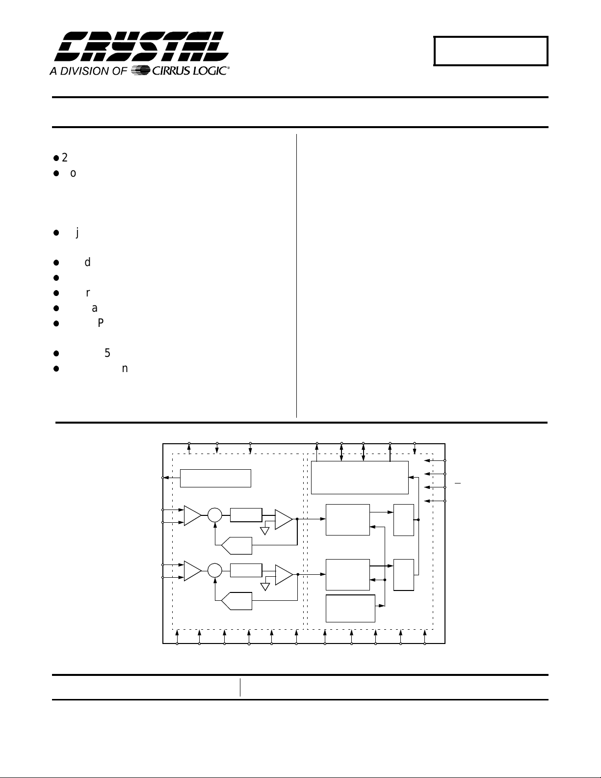
VCOM2MCLKA
1
VREF
AINL-
AINL+
AINR-
AINR+
Voltage Reference
5
4
S/H
26
27
S/H
24
VA
AGND3AGND25AGND
+
-
+
-
Preliminary Product Information
Cirrus Logic, Inc.
Crystal Semiconductor Products Division
P.O. Box 17847, Austin, Texas 78760
(512) 445 7222 FAX: (512) 445 7581
http://www.crystal.com
SCLK SDATA MCLKD
ADCTL
7
6
LP Filter
DAC
LP Filter
DAC
This document contains information for a new product.
Cirrus Logic reserves the right to modify this product without notice.
+
Comparator
+
Comparator
28 23
VL TSTO221VD11DGND
DACTL
9
-
-
LGND22TSTO1
Copyright Cirrus Logic, Inc. 1998
(All Rights Reserved)
LRCK
14 16 20
13
Serial Output Interface
Digital
Decimation
Filter
Digital
Decimation
Filter
Calibration
Microcontroller
8
High
Pass
Filter
High
Pass
Filter
12
15
DGND
19
18
17
10
PDN
DFS
S/M
CAL
MAY ‘98
DS258PP4
1

TABLE OF CONTENTS
ANALOG C H A RA C T E RISTICS ...... .............................. .............................. ......... 3
POWER AND THERMAL CHARACTERISTICS .................................................. 4
DIGITAL FILTER CHARACTERISTICS ...............................................................4
DIGITAL CHARACTERISTICS ............................................................................4
ABSOLUTE MAXIMUM RATINGS ............................................................ ...........5
RECOMMENDED OPERATING CONDITIONS ................................................... 5
SWITCHING CHARACTERISTICS ...................................................................... 6
GENERAL D E SC R IPTION ............. .. ... ............................. ................................... 9
SYSTEM DESIGN ................................................................................................9
Master Clo c k ... ............ ...................................... .............................. ............ 9
SERIAL DATA INTERFACE ................................................................................ 9
Serial Data ..................................................................................................9
Serial Clock .................................................................................................9
Left / Right C lo c k ........ .. .. ..................... ....................................... ..............10
Master Mode .............................................................................................10
Slave Mode ................ ............. .............................................. ....................10
Analog Connections ... ............... .............. .......................... ............... .........10
High Pass Filter ........................................................................................ 11
Power-u p a n d Ca lib r a tio n ............... .. ............ .............................. ..............11
Synchronization of Multiple Devices .........................................................12
Grounding and Power Supply Decouplin g .............................................. ..12
PERFORMANCE ............................................................................................... 12
Digital Filter ............................................................................................... 12
PIN DESCR I P T IO N S .... .. ........... .............................. ....................................... ...14
PARAMETER DEFINITIONS .............................................................................18
REFEREN CES ......... .............. .............. ........... .............. .............. ............. .......... 19
PACKAGE DIMENSIONS ..................................................................................20
CS5394
2 DS258PP4
CS5394
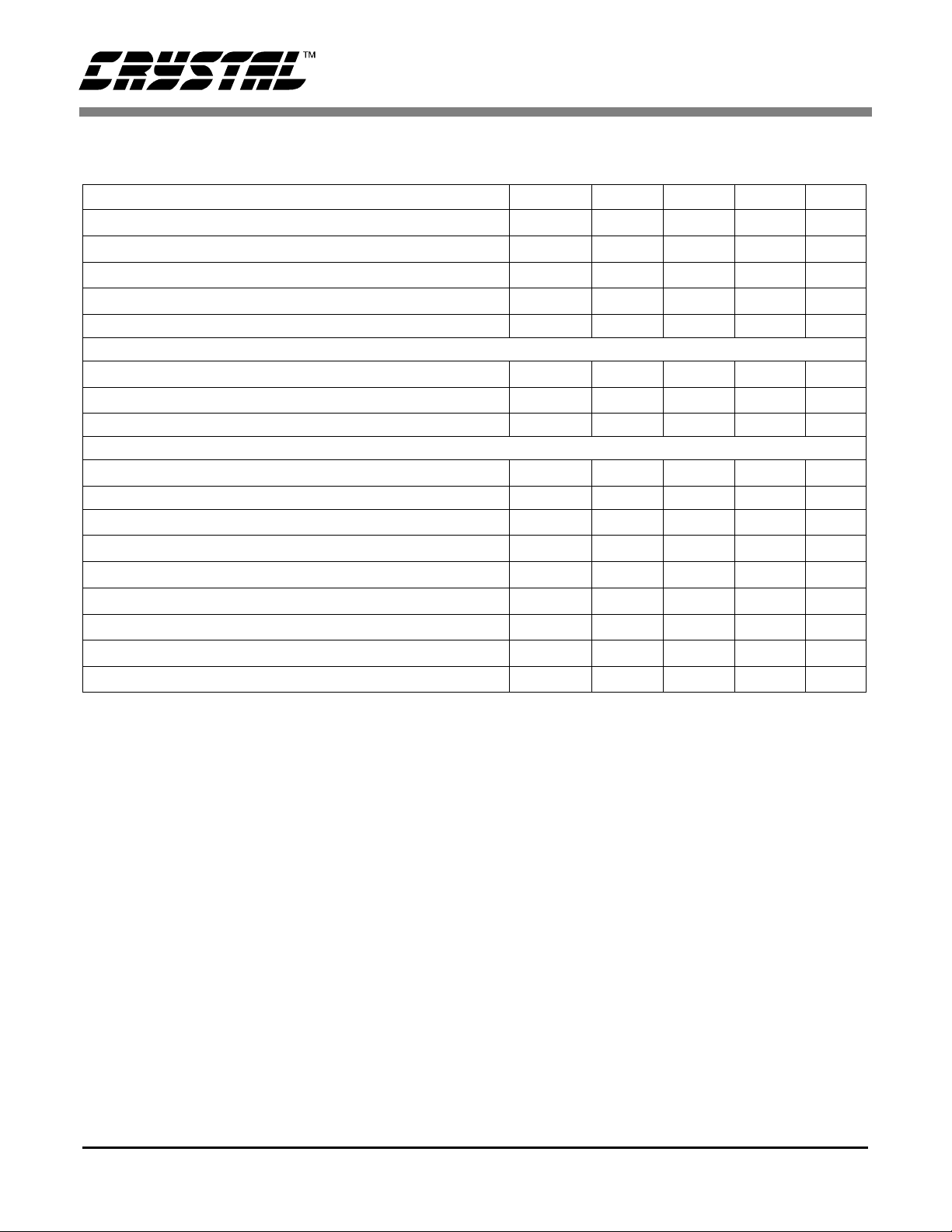
ANALOG CHARACTERISTICS (T
Fs = 48 kHz; SCLK = 3.072 MHz; Analog connections as shown in Figure 1; Measurement Bandwidth is 20 Hz to
20 kHz unless otherwise specifi ed; Logic 0 = 0 V, Logic 1 = VD.)
Parameter Symbol Min Typ Max Unit
= 25 °C; VA, VL, VD = 5 V; Full-scale Input Sinewave, 997Hz;
A
Dynamic Performance
Dynamic Range
A-weighted
Total Harmonic Distortion + Noise (Note 1)
-1.0 dB
-20 dB
-60 dB
Total Harmonic Distortion -1.0 dB (Note 1) THD - 0.0007 TBD %
Interchannel Phase Deviation - 0.01 - Degree
Interchannel Isolation - 118 - dB
THD+N
TBD
TBD
-
-
-
114
117
-103
-94
-54
-
-
TBD
TBD
TBD
dB
dB
dc Accuracy
Interchannel Gain Mismatch - 0.05 - dB
Gain Error - ±5 TBD %
Gain Drift - 100 - ppm/°C
Bipolar Offset Error with High Pass filter - 0 - LSB
Analog Input
Full-scale Differential Input Voltage (Note 2) V
Input Impedance Z
Common-Mode Rejection Ratio CMRR - 82 - dB
Common mode bias Voltage Vcom - 2.5 - V
IN
IN
TBD 4.0 TBD V
-4.5-k
pp
Ω
Notes: 1. Referenced to typical full-scale di fferential input voltage (4.0 Vpp).
2. Specified for a fully differential input ±{(AINR+) - (AINR-)}. Full-scale outputs will be produced for
* Refer to
differential inputs beyond V
Parameter D efinitions
at the end of this data sheet.
Specifications are subject to change without notice
and within VA and AGND.
IN
DS258PP4 3
CS5394
POWER AND THERMAL CHARACTERISTICS (T
= 25 °C; VA, VL, VD = 5 V ±5%;
A
Fs = 48 kHz; Master Mode.)
Parameter Symbol Min Typ Max Unit
Power Supply Current (Normal Operati on) (VA) + (VL)
VD
Power Supply Current (Power-Down Mode) (VA) + (VL)
VD
Power Consumption Normal Operation
Power-Down Mode
I
A
I
D
I
A
I
D
-
-
-
-
-
-
85
65
2
2
750
20
TBD
TBD
-
-
TBD
-
mA
mA
mA
mA
mW
mW
Power Supply Rejection Ratio 1 kHz PSRR - 65 - dB
Allowable Junction Temperature - - 135 °C
Junction to Ambient Thermal I mpedance
DIGITAL FILTER CHARACTERISTICS (T
A
θ
JA
-45-°C/W
= 25 °C; VA, VL, VD = 5 V ±5%; Fs = 48 kHz)
Parameter Symbol Min Typ Max Unit
Passband -0.01 dB (Note 3) 0 - 22.1 kHz
Passband Ripple - - ±0.005 dB
Stop band (Note 3) 26.6 - 3050 kHz
Stop band Attenuation (Note 4) 117 - - dB
Group Delay (Fs = Output Sample Rate) t
Group Delay Variation vs Frequency
gd
∆
t
gd
- 34/Fs - s
--0.0µs
High Pass Filter Characteristics
Frequency Response -3 dB (Note 3)
-0.036 dB
-
-
1.8
20
-
Hz
Phase Deviation @ 20 Hz (Note 3) - 5.3 - Degree
Passband Ripple - - 0 dB
Notes: 3. Filter characteristic scales with sample rate.
4. The analog modulator samples the input at 3.072 MHz for Fs equal to 48 kHz. There is no rejecti on of
input signals which are (n
DIGITAL CHARACTERISTICS (T
× 3.072 MHz) ± 22.1 kHz, where n = 0, 1, 2, 3, ...
= 25 °C; VA, VL, VD = 5 V ±5%)
A
Parameter Symbol Min Max Unit
High-Level Input Voltage
MCLKA/D only
Low-Level Input Voltage
MCLKA/D only
High-Level Output Voltage V
Low-Level Output Voltage V
Input Leakage Current I
V
IH
V
IL
OH
OL
in
2.4
3.0
-
-
-
-
0.8
1.0
V
V
V
V
(VD) - 1.0 - V
-0.4V
-±10µA
4 DS258PP4
CS5394
ABSOLUTE MAXIMUM RATINGS (AGND, DGND = 0 V, All voltages with respect to ground.)
Parameter Symbol Min Max Unit
DC Power Supplies Positive Analog
Positive Logic
Positive Digital
|VA - VD|
|VA - VL|
|VD - VL|
Input Current (Note 5) I
Analog Input Voltage (Note 6) V
Digital Input Voltage (Note 6) V
Ambient Operating Temperature (Power Applied) T
Storage Temperature T
Notes: 5. Any pin except supplies. Transient currents of up to ±100 mA on the analog input pins will not cause
SCR latch-up.
6. The maximum over/under voltage is limited by the input current.
WARNING: Operation at or beyond these limits may result in permanent damage to th e de vice.
Normal operation is not guaranteed at these extremes.
VA
VL
VD
in
INA
IND
A
stg
-0.3
-0.3
-0.3
-
-
-
-±10mA
-0.7 (VA) + 0.7 V
-0.7 (VD) + 0.7 V
-55 +100 °C
-65 +150 °C
+6.0
+6.0
+6.0
0.4
0.4
0.4
V
RECOMMENDED OPERATING CONDITIONS
(AGND, DGND = 0 V, All voltages with respect to ground.)
Parameter Symbol Min Typ Max Unit
DC Power Supplies Positive Analog
Positive Logic
Positive Digital
|VA - VD|
VA
VL
VD
4.75
4.75
4.75
-
5.0
5.0
5.0
-
5.25
5.25
5.25
0.4
V
DS258PP4 5
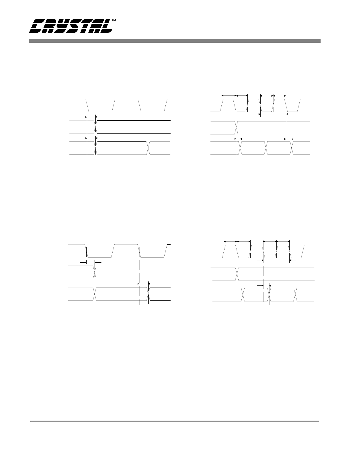
CS5394
SWITCHING CHARACTERISTICS (T
= -10 to 70 ° C; VA = VL = VD = 5 V ± 5%; I nputs:
A
Logic 0 = 0 V
Logic 1 = VA = VL = VD; CL = 20 pF)
Parameter Symbol Min Typ Max Unit
Output Sample Rate F
MCLK Period t
MCLK Low t
MCLK High t
s
clkw
clkl
clkh
2-50kHz
78 - 1950 ns
26 - - ns
26 - - ns
MCLK Fall Time - - 12 ns
Master Mode
SCLK falling to LRCK t
SCLK falling to SDATA valid t
mslr
sdo
-20 - +20 ns
--20ns
SCLK Duty Cycle - 50 - %
Slave Mode
LRCK Period 1/F
s
20 - 500 µs
LRCK Duty Cycle TBD 50 TBD %
SCLK Period t
SCLK Pulse Width Low t
SCLK Pulse Width High t
SCLK falling to SDATA valid t
LRCK edge to MSB valid t
SCLK rising to LRCK edge delay t
LRCK edge to rising SCLK setup time t
sclkw
sclkl
sclkh
dss
lrdss
slr1
slr2
(Note 7) - - ns
(Note 8) - - ns
60 - - ns
- - (Note 9) ns
- - (Note 9) ns
(Note 9) - - ns
(Note 9) - - ns
,
Notes: 7.
8.
9.
1
-----------------128 F
s
1
-----------------256 F
s
1
------------------ 20+
512 F
s
6 DS258PP4
CS5394
SCLK output
t
mslr
LRCK outpu t
t
sdo
SDATA
MSB MSB-1
SCLK to SDATA & LRCK - MASTER Mode
Serial Data Format, DFS low
SCLK output
t
mslr
SCLK input
LRCK input
SDATA
t
slr1tslr2
t
sclkh
t
lrdss
MSB MSB-1 MSB-2
SCLK to LRCK & SDATA - SLAVE Mode
Serial Data Format, DFS low
SCLK input
t
slr1tslr2
t
sclkh
t
sclkl
t
sclkl
t
sclkw
t
t
dss
sclkw
LRCK output
SDATA
SCLK to SDATA & LRCK - MASTER Mode
Serial Data Format, DFS high
2
I
S compatible
t
MSB
sdo
LRCK input
t
dss
SDATA
MSB MSB-1
SCLK to SDATA & LRCK - MASTER Mode
Serial Data Format, DFS high
2
I
S compatible
DS258PP4 7

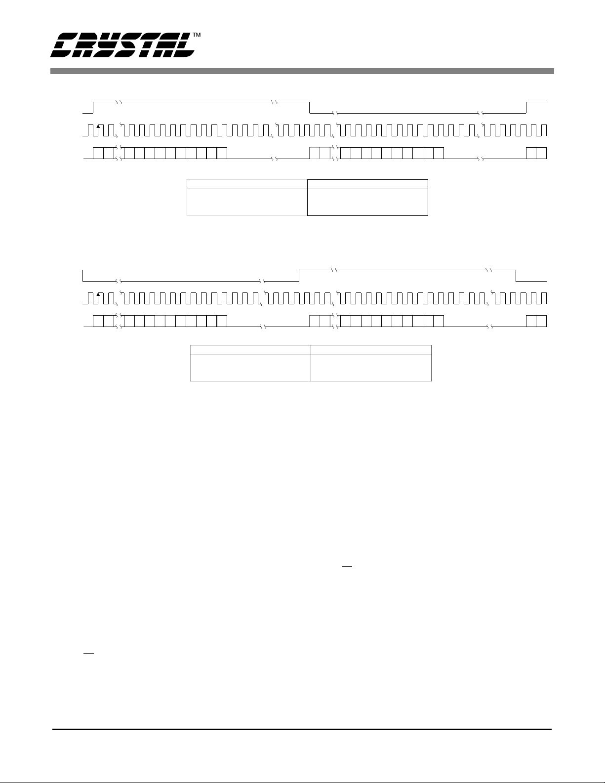
+5V Analog
Ferrite Bead
0.1
CS5394
µ
F
+
+5V Digital
1 µF
+ +
10 µF
+
+
39
39
39
39
Ω
3.9nF
Ω
Ω
3.9nF
Ω
100 µF
Left Analog Input +
Left Analog Input -
Right Analog Input +
Right Analog Input -
1 µF
0.1 µF
0.1 µF
2
27
26
15
0.1
µ
F.1
5.1
Ω
µ
F
112324
1
VA VL
VREF
VD
CAL
PDN
VCOM
DFS
4
5
AINL+
AINL-
AINR+
AINR-
DGND
CS5394
A/D CONVERTER
AGNDLGNDDGND AGND
12
22
* Refer to SDATA Pin Description
28
25
S/M
SDATA*
LRCK
SCLK
MCLKA
MCLKD
DACTL
ADCTL
TSTO1
TSTO2
AGND
3
10
19
18
17
16
13
14
7
20
9
6
8
TSTO pins should be left
21
floating, with no trace
Ferrite bead may be used if
VD is derived from VA. If
used, do not drive any other
logic from VD. An example
ferrite bead is Permag
VK200-2.5/52
Power Down
Calibration Con tr ol
Settings
Processor
Timing Logic
and Clock
and
Mode
Audio
Data
Figure 1. Typical Connection Diagram
8 DS258PP4

CS5394
GENERAL DESCRIPTION
The CS5394 is a 24- bit, stereo A/D conve rter designed for stereo digital audio applications. The device uses a patented, 7th-order tri-level delta-sigma
modulator to sam ple the ana log in put signal s at 64
times the output sample rate (Fs) of the device.
Sample rates of up to 50 kHz are supported. The analog input chan nels ar e simult aneo us ly samp le d by
separate delta-si gma modul ators. The resu lting serial bit streams are digitally filtered, yielding pairs
of 24-bit values. T his technique yiel ds nearly ideal
conversion perfor mance independ ent of input frequency an d amplitude . The c onverte r does no t require difficult-to-design or expensive anti-alias
filters and it doe s not requi re ext ernal sampl e-and hold amplifie rs or voltage referenc es.
An on-chip volt age reference pr ovi de s for a differential input signal range of 4.0 Vpp. The device
also contains a high pass filter, implemen ted digitally afte r the de cimat ion fi lter, t o compl etely el iminate any internal offsets in the converter or any
offsets present at the input to the device. Output
data is av ailable in s erial form , coded as 2 ’s complement 24 -bit number s.
For more information on delta-sigma modulation
techniques see the references at the end of this data
sheet.
SYSTEM DESIGN
are determined by the desired Fs and must be
256x Fs, as shown in Table 1.
LRCK
(kHz)
32 8.192 2.048
44.1 11.2896 2.822
48 12.288 3.072
Table 1. Common Clock Frequencies
MCLKA/D
(MHz)
SCLK
(MHz)
SERIAL DATA INTERFACE
The CS5394 supports two serial data formats
which are selected via the digital format select pin,
DFS. The digital format determines the relationship between the serial data, left/right clock and serial clock. Figures 2 and 3 detail the interface
formats. Th e serial data inte rface is accomp lished
via the serial data output, SDATA, serial data
clock, SCLK, and the left/r ight clock, LRCK. T he
serial nature of the output data results in the left and
right data words being read at different times.
However, the samples within each left/right pair
represent simul ta ne ously sampled an alog inputs.
Serial Data
The serial data block consists of 24 bits of au dio
data present ed in 2’s-complement format with the
MSB-first. The data is clocked from SDATA by
the seri al clock and the channel is det ermined by
the Left/Right clock.
Very few external components are required to support the ADC. Normal power supply decoupling
components, voltage reference bypass capacitors
and a single resistor and capacitor on each input for
isolation are all that ’s required, as shown in Figure
1.
Master Clock
Serial Clock
The serial clock shifts the digitized audio data from
the internal data registers via the SDATA pin.
SCLK is an output in Master Mode where internal
dividers will divide the master clock by 4 to generate a seria l cloc k which is 64 × Fs. In Slave Mode,
SCLK is an inpu t with a se rial clock t ypically between 48× and 128× Fs. It is recommended that
The maste r clock is the clock sour ce for the del tasigma modulator (MCLKA) and digital filters
(MCLKD). The required MCLKA/D frequencies
DS258PP4 9
SCLK be equal to 64× Fs, though other frequencies
are pos si ble, to a void pote ntial int erference e ffects
which may degrade system performance.
CS5394
LRCK
SCLK
SDATA 23 22 7 6 23 22
Left Channel Right Channel
5432108 7654321089 9
MASTER
24-Bit Left Justified Data
Data Valid on Rising Edge of 64x SCLK
MCLK equal to 256x F
s
23 22
SLAVE
24-Bit Left Justified Data
Data Valid on Rising Edge of SCLK
MCLK equal to 256x F
s
Figure 2. Serial Data Format, DFS Low
LRCK
SCLK
SDATA 23 22 8 7 23 22
9 9
Left Channel Right Channel
23 226543210 876543210
MASTER
2
I S 24-Bit Data
Data Valid on Rising Edge of 64x SCLK
MCLK equal to 256x F
s
SLAVE
2
I S 24-Bit Data
Data Valid on Rising Edge of SCLK
MCLK equal to 256x F
s
Figure 3. Serial Data Format, DFS High (I2S compatible)
Left / Right Clock
The Left/Right clock, LRCK, determines which
channel, left or right, is to be output on SDATA. In
Master Mode, LRCK is an output whose frequency
is equal to Fs. In S lave Mode, LRCK is an input
whose frequency m ust be e qua l t o Fs and synchronous to MCLKA/D.
Master Mode
In Master mode, SCLK and LRCK are outputs
which are internally derived from the master clock.
Internal dividers will divide MCLKA/D by 4 to
generate a SCLK whi ch is 64× Fs and by 256 to
generate a LRCK which is equal to Fs. The CS5394
is placed in the Master mode with the slave/master
pin, S/M
, low.
Slave Mode
LRCK and SCLK become inputs in slave mode.
LRCK must be externally derived from MCLKA/D
and be eq ual to Fs. It is rec ommended that SCLK
be equal to 64×. Other frequencies between 48×
and 128× Fs ar e possible but may degrade system
performance due to int erference effects. T he master clock freq uenc y must b e 2 56× F s. Th e C S539 4
is placed in the S lave mo de with th e slave /master
pin, S/M
, high.
Analog Connections
Figure 1 shows t he analog i nput co nnections. The
analog inputs are presented differentially to the
modulators via the AINR+/- and AINL+/- pins.
Each analog input will accept a maximum of
2.0 Vpp. T he + and - input sig nals are 180° out o f
phase resulting in a differential input voltage of
4.0 Vpp. Figure 4 shows the inp ut signal levels for
10 DS258PP4
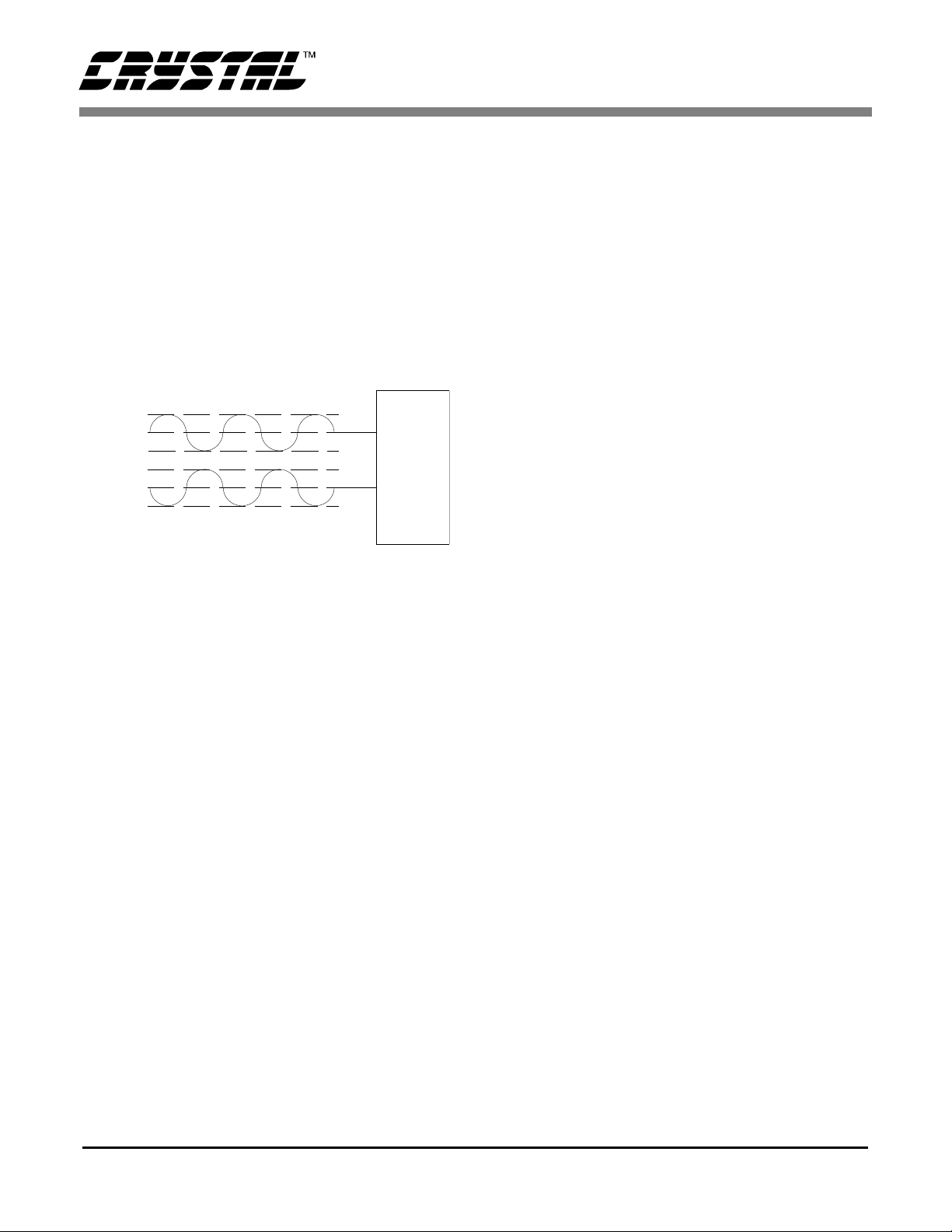
CS5394
full scale. Input si gnals c an be AC or DC coup led.
The VCOM output is available to filter the internal
common mod e and it is reco mmended th at this output be used to bias the analog inp ut buffer to minimize distortio n. However, t his pin is not i ntended
to supply significant amounts of current and is susceptable to noise coupling into the sampling circuits. Please refer to the CDB5394 for a suggested
implementation.
+3.5 V
+2.5 V
+1.5 V
+3.5 V
+2.5 V
+1.5 V
Full Scale Input level= (AIN+) - (AIN-)= 4.0 Vpp
Figure 4. Full Scale Input Voltage
CS5394
AIN+
AIN-
The CS5394 sam ples the analog in puts at 64× Fs,
3.072 MHz for a 48 kHz sampl e-rate. The dig ital
filter rejects all noise above 26.6 kHz except for
frequencies at 3.072 MHz ±22.1 kHz (and multiples of 3.072 MHz). Most audio signals do not have
significant energy at 3.072 MHz. Nevertheless, a
39 Ω resistor in series with each analog input and a
3.9 nF ca pacito r across the inp uts will attenu ate any
noise energy at 3.072 MHz, in a ddition to providing the optimum source impedance for the modulators. The use of capacitors which have a large
voltage coefficient must be avoided since these will
degrade signal linearity. NPO and COG capa citors
are recom mended. If a ctive circuit ry precedes the
ADC, it is recommended that the above RC filter is
placed betw een the a ctive circu itry and the AINR
and AINL pins. The above example frequencies
scale linearly with sample rate.
The on-chip voltage reference is available at VREF
for the purpose of decoupling only. The circuit
traces attached to this pin must be minimal in
length and no load current may be taken from
VREF. The recommended decoupling scheme,
Figure 1, i s a 100 µF electrol ytic capacitor and a
0.1 µF ceram ic capacitor c onnected from VREF to
AGND. The decoupling capacitors, particularly the
0.1 µF, must be positioned to mi nim ize the ele ctrical path from VREF and pin 3, AGND, on the
printed circuit board.
High Pass Filter
The CS5394 includes a high pass filter after the
decimator to remo ve th e indet ermina te DC offset s
introduced by the analog buffer stage and the
CS5394 analog modulator. The first-order high
pass filte r are detail ed in the D igita l Fil ter spe cifi cations table. The filter response scales linearly
with sample rate.
Power-up and Calibration
Reliable power-up can be ac complished by wi thholding the MCLKA/D u ntil the 5 Volt power and
configuration pins are stable. It is also recommended that the MCLKA/D be remo ved if the supplies
drop below 4.75 Volt to prevent power glitch related issues.
The delta-sigma modulators settle in a matter of
microseconds after the analog section is powered,
either t hrough t he a pplic ati on of po wer or b y ex iting the power- down mode. However, the vol tage
reference will take much longer to reach a final value due to the presence of external capacitance on
the VREF pin.
A calibration of the tri-level delta-sigma modulator
should always be initiated following power-up and
after allowing sufficient time for the voltage on the
external VRE F capa ci tor t o se tt le. Thi s i s re quire d
to minimize noise and distortion. Calibration is activated on a ris ing ed ge ap pl ied t o t he CAL pi n and
requires 410 0 LR CK cycl es. It is a lso a dvised th at
the CS5394 be calibrated after the device has
reached thermal equilibrium to maximize performance.
DS258PP4 11

CS5394
Synchronization of Multiple Devices
In systems where multiple ADCs are required, c are
must be taken to achieve simultaneous sampling. It
is recommended that the rising edge of the CAL
signal be timed with a fa lling edge of MCLK to e nsure that all devi ces will initiate a ca libration and
synchronizati on sequence on t he same rising e dge
of MCLK. The absence of re-timing of the CAL
signal can result in a sampling difference of one
MCLK period.
Grounding and Power Supply Decoupling
As with any high resolution converter, the ADC requires careful attention to power supply and
grounding arrangements if its potential performance is to be realized. Figure 1 shows the recommended power arrangements, with VA and VL
connect ed t o a cl ea n +5 V s upp ly. VD, whi ch p owers the digital filter, may be run from the system
+5 V logic supply. Alternatively, VD may be powered from the analog supply via a ferrite bead. In
this case, no additional devices should be powered
from VD. Decoupling capacitors shoul d be as ne ar
to the ADC as possible, with the low value ceramic
capacitor being the nearest.
the modulator s. The VREF decou pling capac itors,
particul ar ly the 0.1 µF, mu st be position ed to minimize the electrical path from VREF and pin 3,
AGND. The CDB5394 evaluation board demonstrates the optimum layout and power supply arrangements, as well as allowing fast evaluati on of
the ADC .
To minimiz e digit al noi se, con nect th e ADC digi tal
outputs only to CMOS inputs.
PERFORMANCE
Digital Filter
Figures 5-8 show the performance of the digital filter included i n the ADC. All plots are no rmalized
to Fs. Assuming a sample rate of 48 kHz, the 0.5
frequency point on the plot refers to 24 kHz. The
filter frequency response scales pre cisely with Fs.
The printed c ircu it boa rd layou t sh ould h ave se parate analog a nd digital re gions and gr ound planes,
with the ADC straddling the boundary. All signals,
especially clocks, should be kept away from the
VREF pin in order to avoid unwanted coupling into
12 DS258PP4

CS5394
Figure 5. CS5394 Stopband Attenuation Figure 6. CS5394 Passband Ripple
Figure 7. CS5394 Transition Band Figure 8. CS5394 Transition Band
DS258PP4 13
PIN DESCRIPTIONS
CS5394
VOLTAGE REFERENCE
COMMON MODE VOLTAGE OUTPUT
ANALOG GROUND
LEFT CHANNEL ANALOG INPUT+
LEFT CHANNE L ANALOG INPUTANALOG CONTROL DATA INPUT
ANALOG SECTION CLOCK INPUT
TEST OUTPUT
CONTROL DA TA OU TPUT
DIGITAL SECTION POWER
DIGITAL GROUND
LEFT/RIGHT CLOC K
SERIAL CLOCK
Power Supply Connections
CALIBRATION
VREF
VCOM
AGND
AINL+
AINL-
ADCTL
MCLKA
DACTL
CAL
VD
DGND
LRCK
1
2
3
4
5
6
7
821
9
10
11
12 17
13
14 15
28
27
26
25
24
23
22
20
19
18
16
AGND
AINR+
AINR-
AGND
VA
VL
LGND
TSTO2TSTO1
MCLKD
PDN
DFS
S/M
SDATA
DGNDSCLK
ANALOG GROUND
RIGHT CHANNEL ANALOG INPUT+
RIGHT CHANNEL ANALOG INPUTANALOG GROUND
POSITIVE ANALOG POWER
ANALOG SECTION LOGIC POWER
ANALOG SECTION LOGIC GROUND
TEST OUTPUT
DIGITAL SECTION CLOCK INPUT
POWER DOWN
SERIAL DATA FORMAT SELECT
SLAVE/MASTER MODE
SERIAL DATA OUTPU T
DIGITAL GROUND
VA - Analog Power, Pin 24.
Positive analog sup ply. Nominally +5 volts.
VL - Logic Power, Pin 23.
Positive logic supp ly for the ana log section. Nominally +5 volts.
AGND - Analog Ground, Pins 3, 25, and 28.
Analog ground reference.
LGND - Logic Ground, Pin 22.
Ground referenc e for the logi c portions of t he analog se ction.
VD - Digital Power, Pin 11 .
Positive supply fo r the digital section. Nomina lly +5 volts.
DGND - Digital Ground, Pins 12 and 15.
Digital ground reference f or the digit al section.
14 DS258PP4

Analog Inputs
AINR-, AINR+ - Differential Right Channel Analog Inputs, Pins 26 and 27.
Analog input connections for the right channel differential inputs. Nominally 4.0 Vpp
differential for fu ll-scale digita l output.
AINL-, AINL+ - Differential Left Channel Analog Inputs, Pins 4 and 5.
Analog input conne ctions for the left ch annel differential in puts. Nominally 4.0 Vpp differen tial
for full-scale dig ital output.
Analog Outputs
VCOM - Common Mode Voltage Output, Pin 2.
Nominally +2.5 volts. Requires a 10 µF electrolytic capacitor in parallel with 0.1 µF ceramic
capacitor for decoupling to AGND. Caution is required if this output be used to bias the analog
input buffer circu its. Refer to th e CDB5394 as an examp le.
CS5394
VREF - Vo ltage Reference Output, Pin 1.
Nominally +4 volts. Requires a 100 µF electrolytic capacitor in parallel with 0.1 µF ceramic
capacitor for decoupling to AGND.
Digital Inputs
ADCTL - Analog Control Input, Pin 6.
Must be connected to DACTL. This signal enables communication between the analog and
digital circui ts.
DFS - Digital Format Select, Pin 18.
The relationship between LRC K, SCLK and SDATA is controlled by the DFS pin. When high,
the serial out put data forma t is I
2
S compatib le. Th e serial d ata forma t is left- justifie d when low.
CAL - Calibration, Pin 10.
Activates the calibration of the tri-level delta-sigma modulator on the rising edge of the CAL
input.
MCLKA - Analog Section Input Clock, Pin 7.
This clock is internally divided and controls the delta-sigma modulators. An MCLKA
frequency of 12.288 MHz sets a modulator sampling rate of 3.072 MHz and a output sample
rate of 48 kHz. MCL KA must be conne cted to MCLKD.
DS258PP4 15

MCLKD - Digital Section Input Clock, Pin 20.
MCLKD clocks the digital filter and must be connected to MCLKA. The required MCLKD
frequency is determi ned by the desired sample rate. A MCLKD of 12.288MHz corresponds to
Fs equal to 48 kHz. MCLKA must be connected to MCLKD.
PDN - Power Down, Pin 19.
When high, the device enters power down. Upon returning low, the device enters normal
operation and issues commands to initialize the voltage reference and synchronize the analog
and digital se ctions of th e device.
S/M
- Slave or Master Mode, Pin 17.
When high, the device is configured for Slave mode where LRCK and SCLK are inputs. The
device is conf igured for Mast er mode where L RCK and SC LK are outpu ts when S/M is low.
Digital Outpu ts
DACTL- Digital to Analog Control Output, Pin 9.
CS5394
Must be connected to ADCTL. This signal enables communication between the digital and
analog ci rcuits.
SDATA - Digital Audio D ata Output, Pin 16.
The 24-bit au dio data is presented MSB first, in 2’s compl ement format. This pin ha s a internal
pull-down resisto r and must remai n low during the po wer-up sequence t o avoid accessin g a test
mode.
Digital Inputs or Outputs
LRCK - Left/Right Clock, Pin 13.
LRCK determines which channel, left or right, is to be output on SDATA. The relationship
between LRCK, SCLK and SDATA is controlled by the Digital Format Select (DFS) pin.
Although the outputs for each channel are transmitted at different times, Left/Right pairs
represent simultaneously sampled analog inputs. In master mode, LRCK is an output whose
frequency is e qual to Fs. In Slave M ode, LRCK is an inp ut whose frequency mu st be equal to
Fs.
SCLK - Serial Data Clock, Pin 14.
Clocks the individual bits of the serial data from SDATA. The relationship between LRCK,
SCLK and SDATA is controlled by the Digital Format Select (DFS) pin. In master mode,
SCLK is an output clock at 64× Fs. In slave mode, SCLK is an input which requires a
continuously sup plied cloc k at any freq uency from 4 8× to 128 × Fs (64× is recom mended).
16 DS258PP4

Miscellaneous
TSTO1, TSTO2 - Test Outpu ts, Pins 8 and 21.
These pins are intended for factory test outputs. They must not be connected to any external
component or a ny lengt h of circuit trace.
CS5394
DS258PP4 17

PARAMETER DEFINITIONS
Dynamic Range
The ratio of the rms value of the signal to the rms sum of all other spectral components over
the specified bandwidth. Dynamic Range is a signal-to-noise ratio measurement over the
specified band wid th made with a -60 dBFS signal. 60 dB is added to resultin g measurement to
refer the measurement to full-scale. This technique ensures that the distortion components are
below the noise le vel and do not effect the measurement. This measurement technique has bee n
accepted by the Audio Engineering Society, AES17-1991, and the Electronic Industries
Association of Japan, EIAJ CP-307 . Expressed in decibel s.
Tot al Harmoni c Distortion + Noi se
The ratio of the rms value of the signal to the rms sum of all other spectral components over
the specified band width (typically 10 Hz to 20 kHz), including distortion components.
Expressed in dec ibels. Measure d at -1 and -20 dBFS as suggest ed in AES17-19 91 Annex A.
Frequency R esponse
A measure of th e amplitude response v ariation from 10 H z to 20 kHz relati ve to the amplitude
response at 1 kHz. Units in decibe ls.
CS5394
Interchannel Isolation
A measure of crosstalk between the left and right channels. Measured for each channel at the
converter’s output with no signal to the input under test and a full-scale signal applied to the
other channel . Units in deci bels.
Interchannel Gain Mismatch
The gain di fference be tween le ft and right channe ls. Units in decibe ls.
Gain Error
The devia tion from th e nominal full-scale analog outp ut for a full- scale digit al input.
Gain Drift
The change in gain value with t empera ture. Un its in ppm /°C.
Offset Error
The deviati on of the mi d-scale transit ion (111...111 t o 000...00 0) from the i deal. Units in m V.
18 DS258PP4

CS5394
REFERENCES
1) "Techniques to Measure and Maximize the Performance of a 120 dB, 96 kHz A/D Comveter Integrated
Circuit” by Steven Harris, Steven Green and Ka Leung. Presented at the 103rd Convention of the Audio Engineering Society, September 1997.
2) "A Stereo 16-bit De lta- Sigma A/D C onvert er for Dig ital Aud io" by D.R. Welland , B. P. Del Signor e,
E.J. Swanson, T. Tanaka, K. Hamashita, S. Hara, K. Takasuka. Paper presented at the 85th Convention
of the Audio Engine ering Society, November 1988.
3) "The Effects of Sampling Clock Jitter on Nyquist Sampling Analog-to-Digital Converters, and on
Oversampling Delta S igma ADC's" b y Steve n Harris. Pa per pr esented at the 8 7th C onventio n of the
Audio Engineer ing Society, Octobe r 1989.
4) "An 18-Bit Dual-Channel Over sampl ing Delta -Sigm a A/D Con verte r, with 19-B it M ono Appli cat ion
Example" by Clif Sanchez. Paper presented at the 87th Convention of the Audio Engineering Society,
October 1989.
5) "How to Achieve Optimum Performance from Delta-Sigma A/D and D/A Converters" by Steven Harris. Presented at the 93rd C onvention of the Aud io Eng ine ering Society, Octob er 1992.
6) "A Fifth-Order Delta- Sigma Modu lator with 110dB Audio Dynam ic Range" by I. Fujimori, K. Hamashita and E.J. Swanson. Paper presented at the 93rd Convention of the Audio Engineering Society,
October 1992.
DS258PP4 19

PACKAGE DIMENSIONS
28L SOIC (300 MIL BODY) PACKAGE DRAWING
1
b
CS5394
E
H
SEATING
PLANE
D
A
e
A1
INCHES MILLIMETERS
DIM MIN MAX MIN MAX
A 0.093 0.104 2.35 2.65
A1 0.004 0.012 0.10 0.30
B 0.013 0.020 0.33 0.51
C 0.009 0.013 0.23 0.32
D 0.697 0.713 17.70 18.10
E 0.291 0.299 7.40 7.60
e 0.040 0.060 1.02 1.52
H 0.394 0.419 10.00 10.65
L 0.016 0.050 0.40 1.27
∝ 0° 8° 0° 8°
c
∝
L
20 DS258PP4

• Notes •

 Loading...