

CS5360
24-Bit Stereo A/D Converter for Digital Audio
Features
l 24 Bit Conversion
l 105 dB Dynamic Range
l -95 dB THD+N
l 128X Oversamplin g
l Fully Differential Inputs
l Linear Phase Digital Anti-Alias Filtering
– 21.7 kHz passband (Fs = 48kHz)
– 85 dB stop band attenuation
– 0.0025 dB pass band ripple
l High Pass Filter - DC Offset Removal
l Peak Signal Level Detector
– High Resolution and Bar Graph Modes
l Pin Compatible wi th CS5334 and CS5 335
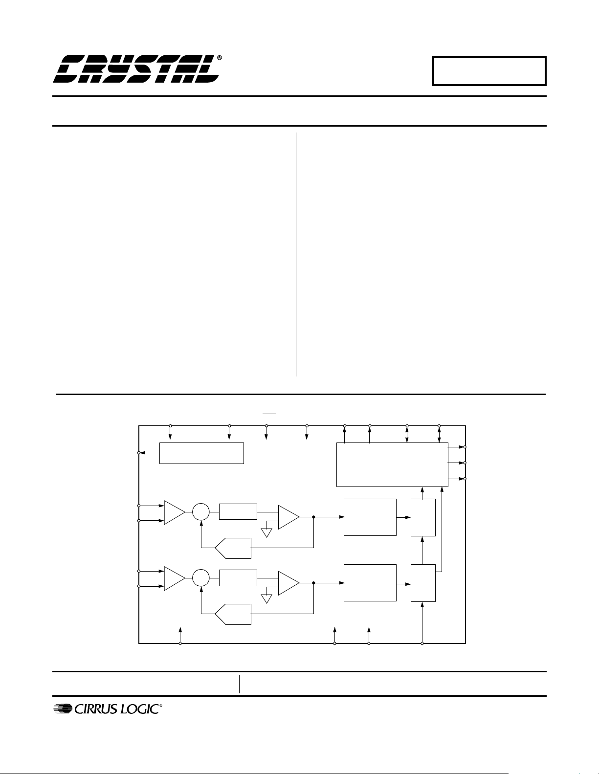
I
CMOUT
AINL-
AINL+
AINR-
AINR+
15
16
17
S/H
14
13
S/H
VA+
3
Voltage Reference
+
-
+
-
VD+
6
LP Filter
DAC
LP Filter
DAC
RST
18
Comparator
Comparator
Description
The CS5360 is a 2- channel, single +5 V supply, 24-bit
analog-to-digital converter for digital audio systems. The
CS5360 performs sampling, analog-to-digital conversion
and anti-alias filte ring, gener ating 24-bit va lues for bot h
left and right inputs in serial form. The output word rate
can be up to 50 kHz per channel.
The CS5360 uses 4th-order, delta-sigma modulation
with 128X oversam pling followed by digital filtering and
decimation, which removes the need for an external antialias filter. This ADC uses a differential architecture
which provides excellent noise rejection.
The CS5360 has a filter passband to 21.7 kHz. The filter
has linear phase, 0.0025 dB passband ripple, and
>85 dB stopband rejection. An on-chip high pass filter is
also included to remove DC offsets.
ORDERING INFORMATION
CS5360-KS -10° to 70°C 20-pin Plastic SSOP
CS5360-BS -40° to 85°C 20-pin Plastic SSOP
MCLK
+
-
+
-
OVFL SCLK LRCK
7
FRAME
2812
10
SDAT A
9
Serial Output Interface
Digital
Decimation
Filter
Digital
Decimation
Filter
High
Pass
Filter
High
Pass
Filter
DIF0
20
DIF1
19
4
AGND
Preliminary Product Information
P.O. Box 17847, Austin, Texas 78760
(512) 445 7222 FAX: (512) 445 7581
http://www.cirrus.com
5
DGND
This document contains information for a new product.
Cirrus Logic reserves the right to modify this product without notice.
Copyright Cirrus Logic, Inc. 1999
(All Rights Reserved)
PU
11
1
HP DEFEAT
DS280PP2
OCT ‘99
1

TABLE OF CONTENTS
1. CHARACTERISTICS AND SPECIFICATIONS .................................. ....... ...... ....... ...... ....... ..... 3
ANALOG CHARACTERISTICS................................................................................................ 3
DIGITAL FILTER CHARACTERISTICS....................................................................................4
DIGITAL CHARACTERISTICS................................................................................................. 4
ABSOLUTE MAXIMUM RATINGS ........................................................................................... 4
SWITCHING CHARACTERISTICS ................................. ...... ....... ...... ....... ...... ....... ...... ............5
2. SYSTEM DESIGN .....................................................................................................................8
2.1 Master Clock ......................................................................................................................8
3. SERIAL DATA INTERFACE ..................................................................................................... 8
3.1 Serial Data .........................................................................................................................8
3.2 Serial Clock ........................................................................................................................ 8
3.3 Left / Right Clock .............................................................................................................. 10
3.4 Master Mode ....................................................................................................................10
3.5 Slave Mode ......................................................................................................................10
3.6 Analog Connections .........................................................................................................10
3.7 High Pass Filter ................................................................................................................ 10
4. INPUT LEVEL MONITORING ................ ....... ...... ....... ...... ...... ....... ...... ....... ...... ....................... 11
4.1 High Resolution Mode ...................................................................................................... 11
4.2 Bar Graph Mode .............................................................................................................. 12
4.3 Overflow ...........................................................................................................................12
4.4 Initialization ......................................................................................................................12
4.5 Initialization with High Pass Filter Enabled ......................................................................12
4.6 Initialization and Internal Calibration with High Pass Filter Disabled ...............................12
4.7 Power-Down .................................................................................................................... 13
4.8 Grounding and Power Supply Decoupling .......................................................................13
4.9 Digital Filter ......................................................................................................................13
5. PIN DESCRIPTIONS ....................................................... ...... ....................................... ...... . ... 15
6. PARAMETER DEFINITIONS ..................................................................................................18
7. PACKAGE DIMENSIONS ....................................................................................................... 19
CS5360
LIST OF FIGURES
Figure 1. SCLK to SDATA & LRCK - MASTER Mode Format 0 and 1 ........................................... 6
Figure 3. SCLK to LRCK & SDATA - SLAVE Mode Format 0 & 1.................................................. 6
Figure 2. SCLK to SDATA & LRCK - MASTER Mode Format 2 .....................................................6
Figure 4. SCLK to LRCK & SDATA - SLAVE Mode Format 2......................................................... 6
Figure 5. SCLK to Frame Delay ...................................................................................................... 6
Contacting Cirrus Logic Support
For a complete listing of Direct Sales, Distributor, and Sales Representative contacts, visit the Cirrus Logic web site at:
http://www.cirrus.com/corporate/contacts/
Preliminary product inf o rmation describes products whi ch are i n production, but for whi ch f ul l characterization data is not yet available. Advance product information describes products which are in development and subject to development changes. Cirrus Logic, Inc. has made best efforts to ensure that the information
contained in this document i s accurat e and reli able. However , t he infor mation is subje ct to chang e without noti ce and is provi d ed “AS IS” without warrant y of
any kind (express or implied). No responsibility is assumed by Cirrus Logic, Inc. for the use of this information, nor for infringements of patents or other ri g ht s
of third parties. This document is the pro perty of Cirrus Logi c, Inc. and i mplie s no licen se under patents, copyrights, tr ademarks, or trade secre ts. No part of
this publication may be copied, reproduced , stored in a retrieval system, or transmitted, in any form or by any means (electronic, mechanical, photographic, or
otherwise) without the pr i or writ ten consent of Cirrus Logic, Inc. It e ms f rom any Ci rrus L ogi c websi t e or di sk may be printed for use by the user. However, no
part of the printout or electronic files may be copied, reproduced, stored in a retrieval system, or transmitted, in any form or by any means (electronic, mechanical,
photographic, or otherwise) without the prior written consent of Cirrus Logic, Inc.Furthermore, no part of this publication may be used as a basis for manufacture
or sale of any items without the prior written consent of Cirrus Logic, Inc. The names of products of Cirrus Logic, Inc. or other vendors and suppliers appearing
in this document may be trademarks or service marks of their respective owners which may be registered in some jurisdictions. A list of Cirrus Logic, Inc. trademarks and service marks can be found at http://www.cirrus.com.
2 DS280PP2

Figure 6. Typical Connection Diagram................ ...... ....... ...... ...... ....... ....................................... .... .7
Figure 7. Data Block and Frame..................................................................................................... 8
Figure 8. Serial Data Format 0.. ............................................................................. ....... ...... ............ 9
Figure 9. Serial Data Format 1.. ............................................................................. ....... ...... ............ 9
Figure 10. Serial Data Format 2...................................................................................................... 9
Figure 11. Full Scale Input Levels................................................................................................. 10
Figure 12. CS5360 Digital Filter Passband Ripple........................................................................ 14
Figure 13. CS5360 Digital Filter Transition Band.......................................................................... 14
Figure 14. CS5360 Digital Filter Stopband Rejection.................................................................... 14
Figure 15. CS5360 Digital Filter Transition Band.......................................................................... 14
LIST OF TABLES
Table 1. Common Clock Frequencies............................................................................................. 9
Table 2. Digital Input Formats......................................................................................................... 9
Table 3. Peak Signal Level Bits - High Resolution Mode.............................................................. 12
Table 4. P7 to P0 - Peak Signal Level Bits -Bar Graph Mode....................................................... 13
CS5360
DS280PP2 3

CS5360
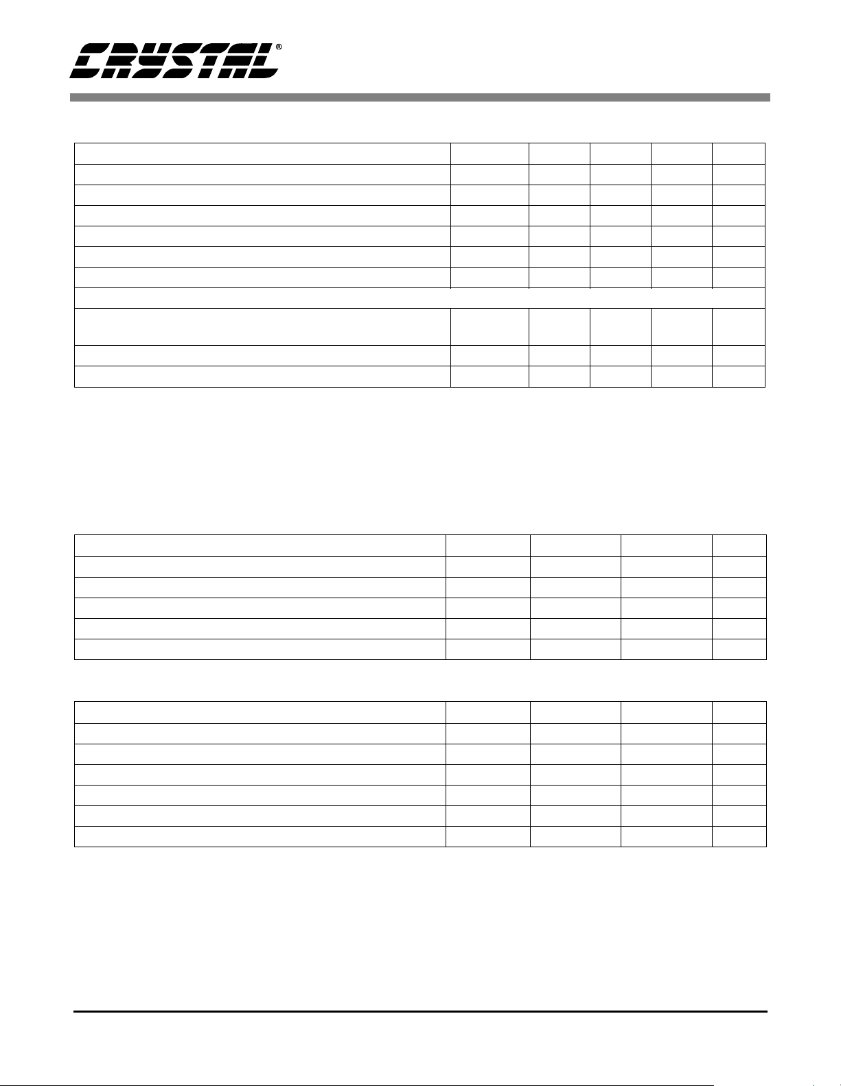
1. CHARACTERISTICS AND SPECIFICATIONS
ANALOG CHARACTERISTICS
(TA = 25 °C; VA+ = VD+ = 5 V; -1 dB Input sinewave, 997 Hz; Fs = 48 kHz; MCLK = 12.288 MHz; SCLK = 3.072
MHz; Measurement Bandwidth is 10 Hz to 20 kHz unless otherwise specified; Logic 0 = 0 V, Logic 1 = VD+)
5360-KS 5360-BS
Parameter Symbol
Temperature Range T
A -10 to +70 -40 to +85 °C
Dynamic Performance
Dynamic Range A-weighted 10097105
102
Total Harmonic Distortion + Noise (Note 1)
-1 dB
-20 dB
-60 dB
Interchannel Phase Deviation - 0.01 - - 0.01 - Degree
Interchannel Isolation (dc to 20 kHz) - 105 - - 105 - dB
THD+N
-
-
-
-95
-82
-42
-
-
-90
-77
-37
95
92
105
102
-
-
-
-95
-82
-42
-85
-72
-32
dc Accuracy
Interchannel Gain Mismatch - 0.05 - - 0.05 - dB
Gain Error - -±5- -±5%
Gain Drift - 200 - - 200 - ppm/°C
Offset Error with HPF
HP defeat with CAL
-
-
0
±100
-
-
-
-
0
±100
Analog Input
Input Voltage Range (Differential) VIN 1.9 2.0 2.1 1.9 2.0 2.1 Vrms
Input Impedance ZIN - 30 - - 30 - k
Input Bias Voltage - 2.2 - - 2.2 - V
Common Mode Rejection Ratio CMRR - 60 - - 60 - dB
Power Supplies
Power Supply Current I
Power Down (IA + ID)
Power Dissipation Normal
Power Down
Power Supply Rejection Ratio - 55 - - 55 - dB
A
I
D
-
-
-
-
-
40
25
0.5
325
2.5
45
30
-
375
-
-
-
-
-
-
40
25
0.5
325
2.5
45
30
375
UnitsMin T yp Max Min Typ Max
-
-
-
-
-
-
dB
dB
dB
dB
LSB
LSB
Ω
mA
mA
mA
mW
mW
Notes: 1. Referenced to nominal input level.
Specifications are subject to change without notice
4 DS280PP2
CS5360
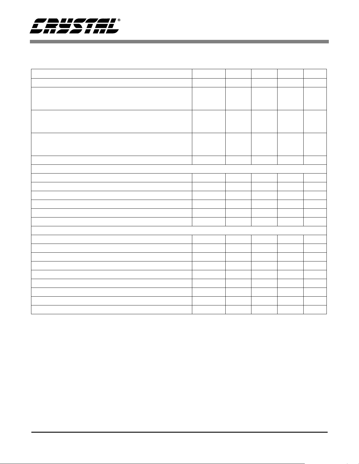
DIGITAL FILTER CHARACTERISTICS (Note 2, T
= 25 °C; VA+ = VD+ = 5 V ±5%; Fs = 48 kHz)
A
Parameter Symbol Min Typ Max Unit
Passband (Note 3) 0.02 - 21.7 kHz
Passband Ripple - - ±0.0025 dB
Stopband (Note 3) 26.3 - 6118 kHz
Stopband Attenuation (Note 4) 85 - - dB
Group Delay (Fs = Output Sampl e Rate) t
Group Delay Variation vs. Frequency
gd
∆
t
gd
- 32/Fs - s
--0µs
High Pass Filter Characteristics
Frequency Response -3 dB (Note 3)
-0.1 dB
-
-
0.9
20
-
Hz
Phase Deviation @20 Hz (Note 3) - 2.6 - Degree
Passband Ripple - - 0 dB
Notes: 2. Filter response is not tested but is guaranteed by design.
3. Filter characteristics scale with output sample rate.
4. The analog modulator samples the input at 6.144 MHz for an output sample rate of 48 kHz. There is
no rejection of input signals which are multiples of the sampling frequency (n x 6.144 MHz ±21.7 kHz
where n = 0, 1, 2, 3, ...).
DIGITAL CHARACTERISTICS (T
= 25 °C; VA+ = VD+ = 5 V ±5%)
A
Parameter Symbol M in Max Unit
High-level Input Voltage V
Low-level Input Voltage V
High-level Output Voltage at Io = -20 µA V
Low-level Output Voltage at Io = 20 µA V
Input Leakage Current I
IH
IL
OH
OL
in
2.4 - V
-0.8V
(VD+) - 1.0 - V
-0.4V
-10µA
ABSOLUTE MAXIMUM RATINGS (AGND = 0 V, all voltages with respect to ground.)
Parameter Symbol M in Max Unit
DC Power Supply VA+ -0.3 +6.0 V
Input Current, Any Pin Except Supplies (Note 5) I
Analog Input Voltage (Note 6) V
Digital Input Voltage (Note 6) V
Ambient Temperature (power applied) T
Storage Temperature T
in
INA
IND
A
stg
Notes: 5. Any pin except supplies. Transient currents of up to ±100 mA on the analog input pins will not cause
SCR latch-up.
6. The maximum over/under voltage is limited by the input extremes.
WARNING: Operation at or beyond these limits may result in permanent damage to the device.
Normal operation is not guaranteed at these extremes.
- ±10 mA
-0.7 (VA+) + 0.7 V
-0.7 (VA+) + 0.7 V
-55 +125 °C
-65 +150 °C
DS280PP2 5
CS5360
1
1024
()
F
S
()
------------------------------- 30 n s+
SWITCHING CHARACTERISTICS (T
Logic 1 = VA+ = VD+; C
= 20 pF)
L
= 25 °C; VA+ = 5 V ±5%; Inputs: Logic 0 = 0 V,
A
Parameter Symbol Min Typ Max Unit
Output Sample Rate F
MCLK Period MCLK / LRCK = 256
t
MCLK / LRCK = 384
MCLK / LRCK = 512
MCLK Low MCLK / LRCK = 256
MCLK / LRCK = 384
MCLK / LRCK = 512
MCLK High MCLK / LRCK = 256
t
MCLK / LRCK = 384
MCLK / LRCK = 512
Peak Update Pulse Width pu
S
clkw
t
clkl
clkh
pulse
8.0 - 50 kHz
78
52
39
31
20
15
31
20
15
-
-
-
-
-
-
-
-
-
1953
1302
976
-
-
-
-
-
-
20 - - ns
Master Mode
SCLK Falling to LRCK (Note 7) t
SCLK Falling to SDATA Valid (Note 7) t
mslr
sdo
-10 - 10 ns
-10 - 35 ns
SCLK Duty Cycle - 50 - %
SCLK Falling to Frame Valid (Note 7) t
LRCK Edge to OVFL Valid t
LRCK Edge to OVFL Edge Delay t
sfo
ovfl
ovfl
-10 - Note 8 ns
-10 - 30 ns
-10 - Note 12 ns
Slave Mode
LRCK Duty Cycle 25 50 75 %
SCLK Period t
SCLK Pulse Width Low (Note 10) t
SCLK Pulse Width High (Note 11) t
SCLK Falling to SDATA Valid (Note 7) t
LRCK Edge to MSB Valid t
SCLK Rising to LRCK Edge Delay (Note 14) t
LRCK Edge to Rising SCLK Setup Time (Note 14) t
SCLK Falling to Frame Delay t
sclkw
sclkl
sclkh
dss
lrdss
slr1
slr2
sfo
Note 9 - - ns
Note 13 - - ns
50 - - ns
- - Note 13 ns
- - Note 13 ns
50 - - ns
Note 13 - - ns
- - Note 15 ns
Notes: 7. SCLK Rising for Mode 1
8.
1
------------------- -----
9.
()
()
96
F
S
10. Pulse Width High for Mode 1
11. Pulse Width Low for Mode 1
12.
13.
1
------------------- -------- -20 ns+
()
()
512
F
S
1
----------------------------50 ns+
()
()
512
F
S
14. SCLK Falling for Mode 1
15.
1
----------------------------35 ns+
()
()
384
F
S
ns
ns
ns
6 DS280PP2
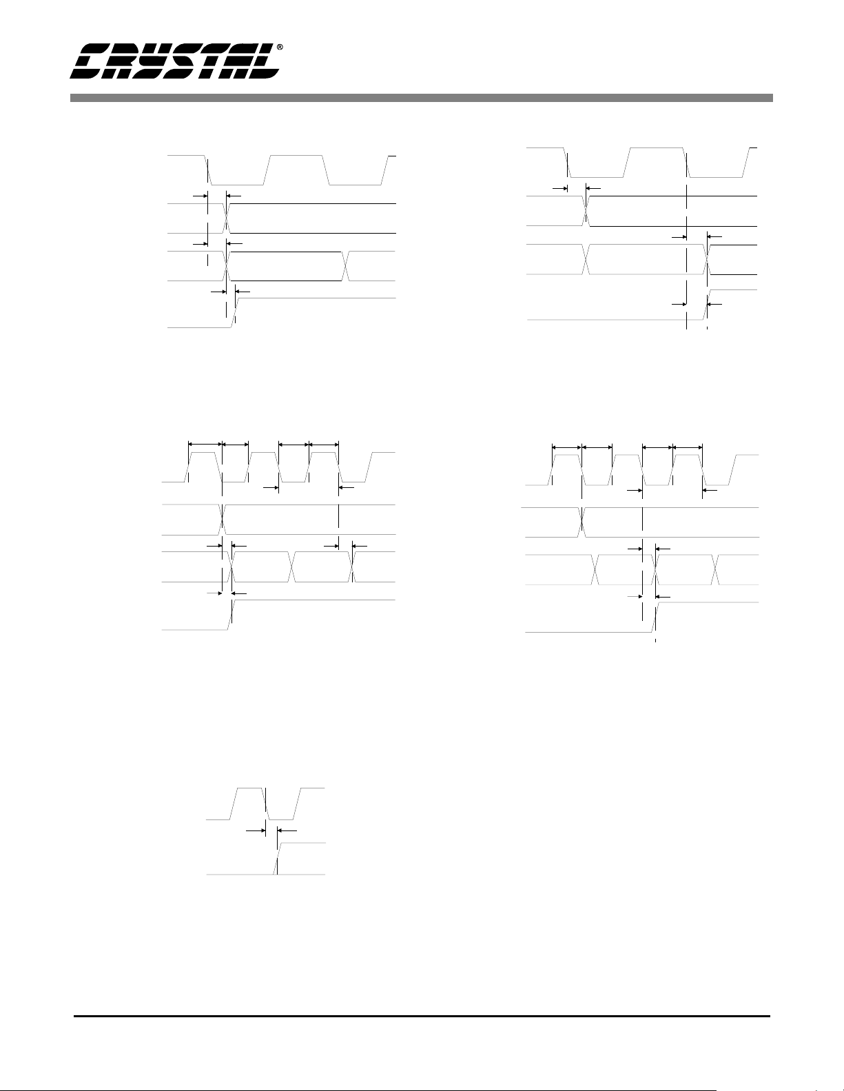
Figure 1. SCLK to SDATA & LRCK - MASTER Mode
Format 0 and 1
Figure 3. SCLK to LRCK & SDATA - SLAVE Mode
Format 0 & 1
SCLK*
FRAME
t
sfo
CS5360
SCLK output*
LRCK output
SDATA
OVFL
SCLK input*
(SLAVE mode)
LRCK input
(SLAVE mode)
SDATA
OVFL
t
ovfl
slr1tslr2
t
mslr
t
sdo
MSB MSB-1
t
t
lrdss
MSB MSB-1 MSB-2
t
ovfl
t
sclkl
t
sclkh
t
sclkw
t
dss
SCLK output
t
mslr
LRCK output
t
sdo
SDATA
OVFL
MSB
t
ovfl
Figure 2. SCLK to SDATA & LRCK - MASTER Mode
Format 2
SCLK input
(SLAVE mode)
LRCK input
(SLAVE mode)
SDATA
OVFL
t
slr1tslr2
t
sclkl
t
sclkh
t
sclkw
t
dss
MSB MSB-1
t
ovfl
Figure 5. SCLK to Frame Delay
* SCLK is inverted in Format 1
DS280PP2 7
Figure 4. SCLK to LRCK & SDATA - SLAVE Mode
Format 2

LeftAnalog
LeftAnalog
RightAnalog
RightAnalog
*
**
+
150
Input +
150
Input-
150
Input +
150
µ
1
F0.1
Ω
2.2 nF
Ω
Ω
2.2 nF
Ω
17
16
15
13
14
Input -
Required for Master Mode only
Required for Bar Graph Mode only
µ
F
VD+
AINL+
AINL-
CMOUT
AINR+
AINR-
Ω
2
63
VA+
PU
2
47 k
11
1
20
19
100
9
100
12
CS5360
HP DEFEAT
OVFL
DIF0
DIF1
SDATA
LRCK
100
SCLK
8
100
MCLK
RST
FRAME
7
18
10
47 k
1
Ω
Ω
Ω
Ω
Ω
Ω
+
µ
F0.1µF
*
**
CS5360
+5V Analog
Peak Signal
Level Monitor
Mode
Settings
Audio Data
Processing
Timing, Logic
&
Clock
DGND AGND
54
Figure 6. Typical Connection Diagram
8 DS280PP2

CS5360
2. SYSTEM DESIGN
The CS5360 is a 24-bit, 2-channel analog-to-digital
converter designed for digital audio applications.
This device uses two one-bit delta-sigma modulators which simultaneously sample the analog input
signals at 128 times the output sample rate (Fs).
The resulting serial bit streams are digitally filtered, yielding a pair of 24-bit values. This technique yields nearly ideal conversion performance
independent of input frequency and amplitude. The
converter does not require difficult-to-design or expensive anti-alias filters and does not requi re external sample-and-hold amplifiers or a voltage
reference. Very few external components are required to support this ADC. Normal power supply
decoupling components and a resistor and capacitor on each input for anti-aliasing are the only external components required, as shown in Figure 6.
An on-chip voltage reference provides for a differential input signal range of 2.0 Vrms. Output data
is available in serial form, coded as 2’scomplement,
24-bit numbers. Typical power consumption is
325 mW which can be reduced to 1.0 mW by using
the power-down feature.
3. SERIAL DATA INTERFACE
The CS5360 supports three serial data formats, including I2S, selected via the di gita l int e rface f o rmat
pins DIF0 and DIF1. The digital interface format determines the relationship between the serial data,
left/right clock and serial clock. Table 2 lists the
three formats and their associated figure number.
The serial data interface is acc omplis hed via th e serial data output, SDATA, serial data clock, SCLK,
and the left/right clock, LRCK.
DIF1 DIF0 FORMAT FIGURE
0008
0119
10210
1 1 power-down -
Table 2. Digital Input Formats
3.1 Serial Data
The serial data block consists of 24 bits of audio
data presented in 2’s-complement format with the
MSB-first followed by 8 Peak Signal Level, PSL,
bits as shown in Figure 7. The data is clocked from
SDATA by the serial clock and the channel is determined by the Left/Right clock.
2.1 Master Clock
The master clock (MCLK) is the clock source f or
the delta-sigma modulator and digital filters. In
SDATA
24 Audio
Data Bits
21 20 19 18
8 PSL Bits
P723 22 1 0 P6 P1 P0
Master Mode, the frequency of this clock must be
256x Fs. In SlaveMode, the master clock must be
FRAME
either 256x, 384x or 512x Fs. Table 1 shows some
common master clock frequencies.
LRCK
(kHz)
32 8.1920 12.2880 16.3840
44.1 11.2896 16.9344 22.5792
48 12.2880 18.4320 24.5760
256 X 384 X 512 X
MCLK (MHz)
3.2 Serial Clock
The serial clock shifts t he digital audio data from the
internal data registers via the SDATA pin. SCLK is
an output in Master Mode. Internal dividers will di-
Figure 7. Data Block and Frame
vide the master clock by 4 to generate a serial clock
Table 1. Common Clock Frequencies
which is 64x Fs. In Slave Mode, SCLK is an input
with a serial clock typically between 48x and 96x Fs.
However, the serial clock must be a minimum of 64x
Fs to access the Peak Signal Level bits.
DS280PP2 9

CS5360
LRCK
(64X) SCLK
SDATA P1 P023 22 1 P7 P6 P5 P4 P3 P20 23 22
P0
FRAME
LEFT RIGHT
P1 P02322 1 P7P6P5P4P3P2021 20 21 2019 18 19 185432 5432
MASTER SLAVE
24-Bit Left Justified Data 24-Bit Left Justified Data
Data Valid on Rising Edge of 64x SCLK Data Valid on Rising Edge of SCLK
MCLK equal to 256x Fs MCLK equal to 256x, 384x, or 512x Fs
Figure 8. Serial Data Format 0
LRCK
(64X) SCLK
SDATA P1 P023 22 1 P7 P6 P5 P4 P3 P20 23 22
FRAME
LEFT RIGHT
P1 P02322 1 P7P6P5P4P3P2021 20 21 2019 18 19 185432 5432P0
ASTER SLAVE
Data 24-Bit Left Justified Data
g Edge of 64x SCLK Data Valid on Falling Edge of SCLK
x Fs MCLK equal to 256x, 384x, or 512x Fs
Figure 9. Serial Data Format 1
LRCK
(64X) SCLK
SDATA P1 P023 22 1 P7 P6 P5 P4 P3 P20 23 22
FRAME
LEFT R IGHT
P1 P02322 1 P7P6P5P4P3P2021 20 21 2019 18 19 18P0 5432 5432
MASTER SLAVE
2
S 24-Bit Left Justified Data I2S 24-Bit Left Justified Data
I
Data Valid on Rising Edge of 64x SCLK Data Valid on Rising Edge of SCLK
MCLK equal to 256x Fs MCLK equal to 256x, 384x, or 512x Fs
Figure 10. Serial Data Format 2
10 DS280PP2

CS5360
3.3 Left / Right Clock
The Left/Right clock determines which channel,
left or right, is to be output on SDATA. Although
the outputs for each channel are transmitted at different times, Left/Right pairs represent simultaneously sampled analog inputs. In Master Mode,
LRCK is an output whose frequency is equal to Fs.
In Slave Mode, LRCK is an input whose frequency
must be equal to the output sample rate, Fs.
3.4 Master Mode
In Master mode, SCLK and LRCK are outputs
which are internally derived from the Master
Clock. Internal dividers will divide MCLK by 4 to
generate a SCLK which is 64x Fs and by 256 to
generate a LRCK which is equal to Fs. Master
mode is only supported with a 256x master clock.
The CS5360 is placed in the Master mode with a
47 kΩ pull-down resistor on the OVFL pin.
3.5 Slave Mode
LRCK and SCLK become inputs in SLAVE mode.
LRCK must be externally derived from MCLK and
be equal to Fs. The serial clock is typically between
64x and 96x Fs. A 48x Fs serial clock is possible
though will not allow access to the Peak Signal
Level bits. Master clock frequencies of 256x, 384x
and 512x Fs are supported. The ratio of the applied
master clock to the left/right cloc k is automa tic ally
detected during power-up and internal dividers are
set to generate the appropriate internal clocks.
3.6 Analog Connections
Figure 6 shows the analog input connections. The
analog inputs are presented to the modulators via
the AINR+/- and AINL+/- pins. Each analog input
pin will accept a maximum of 1Vrms centered at
+2.2 Volt as shown in Figure 11. Input signals can
be AC or DC coupled and the CMOUT output may
be used as a reference for DC coupling. However,
CMOUT is not buffered, and the maximum current
is 10 µA.
3.6 V
2.2 V
0.78 V
3.6 V
2.2 V
0.78 V
Full Scale Input level= (AIN+) - (AIN-)= 5.67 Vpp
Figure 11. Full Scale Input Levels
CS5360
AIN+
AIN-
The CS5360 samples the analog inputs at 128x Fs,
6.144MHz for a 48kHz sample-rate. The digital filter rejects all noise above 26.3kHz except for frequencies right around 6.144MHz ±21.7kHz (and
multiples of 6.144MHz). Most audio signals do not
have significant energy at 6.144MHz. Nevertheless, a 150 Ω resistor in series with each analog input and a 2.2 nF capacitor across the inputs will
attenuate any noise energy at 6.144MHz, in addition to providing the optimum source impedance
for the modulators. The use of capacitors which
have a large voltage coefficient must be avoided
since these will degrade signal linearity. NPO and
COG capacitors are accept able. If active circuitry
precedes the ADC, it is recommended that the
above RC filter is placed between the active circuitry and the AINR and AINL pins. The above example frequencies scale linearly with the sample rate.
3.7 High Pass Filter
The operational amplifiers in the input circuitry
driving the CS5360 may generate a small DC offset
into the A/D converter. The CS5360 includes a
high pass filter after the decimator to remove any
DC offset which could result in recording a DC level, possibly yielding "clicks" when switching between devices in a multichannel system. The high
pass filter can be disabled with the HP DEFEAT
pin.
The high pass filter works by continuously subtracting a measure of the dc offset f rom the output
of the decimation filter. If the HP DEFEAT pin is
DS280PP2 11

CS5360
taken high during normal operation, the current
value of the dc offset register is frozen and this dc
offset will continue to be subtracted from the conversion result. This feature makes it possible to perform a system calibration by:
1) removing the signal source (or grounding the
input signal) at the input to the subsystem containing the CS5360,
2) running the CS5360 with the HP DEFEAT pin
low (high pass filter enabled) until the filter settles (approximately 1 second), and
3) taking the HP DEFEAT pin high, disabling the
high pass filter and freezing the stored dc off set.
A system calibration performed in this way will
eliminate offsets anywhere in the signal path between the calibration point and the CS5360.
The characteristics of the first-order high pass filter
are outlined below for an output sample rate of
48 kHz. This filter response scales linearly with
sample rate.
Frequency response: -3 dB @ 0.9 Hz
-0.01 dB @ 20 Hz
Phase deviation: 2.6 degrees @ 20 Hz
Passband ripple: None
4. INPUT LEVEL MONITORING
The CS5360 includes independent Peak Input Level Monitoring for each channel. The analog-to-digital converter continually monitors the peak digital
signal for both channels, prior to the digital limiter,
and records these values in the Active registers.
This information can be transferred to the Output
registers by a high to low transition on the Peak Update pin (PU) which will also reset the Active register. The Active register contains the peak signal
level since the previous peak update request.
The 8-bit contents of the output registers are available in all interface modes and are present in the
data block as shown in Figure 7. The monitoring
function can be formatted to indicate either High
Resolution Mode or Bar Graph Mode. The monitoring function is determined on power-up by the
presence of a 47 kΩ pull-down resistor on
FRAME. The addition of a 47 kΩ pull-down resistor on the FRAME pin sets the monitoring function
to the Bar Graph mode.
4.1 High Resolution Mode
Bits P7-P0 indicate the peak input level since the
previous peak update (or low transition on the Peak
Update pin). If the full scale input level is exceeded
(Bit P7 high), bits P5-P0 represent the peak value
up to 3 dB above full-scale in 1 dB steps. If the
ADC input level is less than full-scale, bits P5-P0
represent the peak value from -60 dB to 0 dB of full
scale in 1 dB steps. The PSL outputs are accurate to
within 0.25 dB. Bit P6 provides a coarse means of
determining an ADC input idle condition. Bit P7
indicates an ADC overflow condition, if the ADC
input level is greater than full-scale.
P7 - Overrange
0 - Analog input less than full-scale level
1 - Analog input greater than full-scale
P6 - Idle channel
0 - Analog input >-60 dB from full-scale
1 - Analog input <-60 dB from full-scale
P5 to P0 - Peak Signal Level Bits (1 dB steps)
Inputs <0 dB P5 - P0
0 dB 000000
-1 dB 000001
-2 dB 000010
-60 dB 111100
Inputs >0 dB P5 - P0
0 dB 000000
+1 dB 000001
+2 dB 000010
+3 dB 000011
Table 3. Peak Signal Level Bits - High Resolution Mode
12 DS280PP2

CS5360
4.2 Bar Graph Mode
This mode provides a decoded output format which
indicates the peak Peak Signal Level in a "Bar
Graph" format.
Input Level P7 - P0
Overflow 11111111
0 dB to -3 dB 01111111
-3 dB to -6 dB 00111111
-6 dB to -10 dB 00011111
-10 dB to -20 dB 00001111
-20 dB to -30 dB 00000111
-30 dB to -40 dB 00000011
-40 dB to -60 dB 00000001
< - 60 dB 00000000
Table 4. P7 to P0 - Peak Signal Level Bits -Bar Graph
Mode
4.3 Overflow
Overflow indicates analog input overrange for the
Left and Right channels as of the last update request on the Peak Update pin. A value of 1 indicates an overrange condition. The left channel
information is output on OVFL during the left
channel portion of LRCK. The right channel information is available on OVFL during the right channel portion of LRCK.
4.4 Initialization
Upon initial power-up, the digital filters and deltasigma modulators are reset and the internal voltage
reference is powered down. The CS5360 will remain in the power-down mode until valid clocks
are presented. A valid MCLK is required to exit
power-down in Master Mode. However, in Slave
Mode, MCLK and LRCK of the proper ratio are required to exit power-down. MCLK occurrences are
also counted over one LRCK period to determine
the MCLK / LRCK frequency ratio in Slave Mode.
Power is then applied to the internal voltage reference, the analog inputs will move to approximately
2.2 V and output clocks will begin (Master Mode
only). This process requires 32 periods of LRCK
and is followed by the initialization sequence.
4.5 Initialization with High Pass Filter Enabled
28,672 LRCK cycles are required for the initialization sequence with the high pass filter enabled.
This time is dominated by the settling time require d
for the high pass filter.
4.6 Initialization and Internal Calibration with High Pass Filter Disabled
If the HP DEFEAT pin is high (high pass filter disabled) during the initialization sequence, the
CS5360 will perform an internal dc calibration by:
1) disconnecting the internal ADC inputs from the
input pins,
2) connecting the (differential) ADC inputs to a
common reference voltage,
3) running the high pass filter with a fast settling
time constant,
4) freezing the dc offset register, and
5) reconnecting the internal ADC inputs to the in-
put pins.
This procedure takes 4,160 cycles of LRCK. Unlike the system calibration procedure described in
the High Pass Filter section, a dc calibration performed during start-up will only eliminate offsets
internal to the CS5360, and should result in output
codes which accurately reflect the differential dc
signal at the pins.
DS280PP2 13

CS5360
4.7 Power-Down
The CS5360 has a power-down mode wherein typical consumption drops to 1.0 mW. This is initiated
when a loss of clock is detected (either LRCK or
MCLK in Slave Mode or MCLK in Master Mode),
RST is enabled or DIF0 / DIF1 are at a logic 1. The
initialization sequence will begin whenever valid
clocks are restored, RST is disabled and DIF0 /
DIF1 are restored. If the MCLK / LRCK frequency
ratio changes during power-down, the CS5360 will
adapt to these new operating conditions. However,
only the RST method of power-down will include
the Master/Slave decision in the initialization sequence.
4.8 Grounding and Power Supply Decoupling
As with any high resolution converter, the CS5360
requires careful attention to power supply and
grounding arrangements to optimize performance.
Figure6 shows the recommended power arrangements with VA+ connected to a clean +5volt supply. VD+ should be derived from VA+ through a 2
ohm resistor. VD+ should not be used to power additional digital circuitry. All mode pins which require VD+ should be connected to pin 6 of the
CS5360. All mode pins which require DGND
should be connected to pin 5 of the CS5360.
AGND and DGND, Pins 4 and 5, should be connected together at the CS5360. DGND for the
CS5360 should not be confused with the ground for
the digital section of the system. The CS5360
should be positioned over the analog ground plane
near the digital / analog ground plane split. The analog and digital ground planes must be connected
elsewhere in the system. The CS5360 evaluation
board, CDB5360, demonstrates this layout technique. This technique minimizes digital noise and
insures proper power supply matching and sequencing. Decoupling capacitors should be located
as near to the CS5360 as possible.
4.9 Digital Filter
Figures 12-15 show the performance of the digital
filter included in the CS5360. All plots are normalized to Fs. Assuming a sample rate of 48 kHz, the
0.5 frequency point on the plot refers to 24 kHz.
The filter frequency response scales precisely with
the sample rate.
14 DS280PP2

Figure 12. CS5360 Digital Filter Passband Ripple
Figure 14. CS5360 Digital Filter Stopband Rejection
CS5360
Figure 13. CS5360 Digital Filter Transition Band
DS280PP2 15
Figure 15. CS5360 Digital Filter Transition Band

5. PIN DESCRIPTIONS
CS5360
High Pass Filter De f eat
Overflow
Analog Power
Analog Ground
Digital Gr ou nd
Digit a l Power
Master Clock
HPDEFE AT
OVFL
VA+
AGND
DGND
VD+
MCLK
Serial Data Clock
Serial Data Output
SDATA
Frame Signal
High Pass Filter Defeat - HP DEFEAT
Pin 1, Input
Functio n
A high logic leve l on this pin disables the digital high pass filter. A low logic lev el on this pin enable s the
high pass filter.
Overflow - OVFL
Pin 2, Input
Functio n
Overflow indicates analog input overrange, for both the Left and Right channels, since the last update
request on the PEAK U PDATE (PU ) pin. A value of 1 in the register indica tes an overrange condition.
The left channel information is output on OVFL during the left channel portion of LRCK. The right
channel information is available on OVFL during the right channel portion of LRCK. The registers are
updated with a high to l ow transition on the PEAK UPDATE pin. A 47 kΩ pull-down resist or on this pin
will set the CS5360 in Maste r Mode.
1
2
3
4
5
6
7
813
9
10 11
20
19
18
17
16
15
14
12
DIF0
DIF1
RST
AINL+
AINL-
CMOUT
AINR-
AINR+SCLK
LRCK
PUFRAME
Digital Interface Format 0
Digital Interface Format 1
Reset
Non-Inverting Left Channel Input
Inverting Left Channel Input
Common Mode Output
Inverting Right Channel Input
Non-Inverting Right Channel Input
Left / Right Clock
Peak Update
Positive Analog Power - VA+
Pin 3, Input
Function:
Positive analog supp ly. Nominally +5 volts.
Analog Ground - AGND
Pin 4, Input
Function:
Analog ground reference .
DGND - Digital Ground
Pin 5, Input
Function:
Digital ground reference.
16 DS280PP2

Positive Di gital Power - V D+
Pin 6, Input
Function:
Positive digital supply. Nominally +5 volts.
Master Clock - MCLK
Pin 7, Input
Function:
Clock source for the delta-si gma modulator sampl ing and digital filte rs. In Master Mode, the fr equency of
this clock must be 256x the outp ut sample rate, Fs. In Slave Mode, the frequenc y of this clock must be
either 256x, 384x or 512 x Fs.
Serial Data Clock - SCLK
Pin 8, Input/Output
Function:
Clocks the individual bits of the serial data out from the SDATA pin. The relationship between LRCK,
SCLK and SDATA is controlled by DIF0 and DIF1.In Master Mode, SCLK is an output clock with a
frequency of 64x the outpu t sample rate, Fs.In Slave M ode, SCLK is an input.
Serial Data Output - SDATA
Pin 9, Output
Function:
Two’s complement MSB-first se rial data of 24 bits is output on this pin. Included in the serial data output
is the 8-bit Input Signal Level Bits. The data is clocked out via the SCLK clock and the channel is
determined by LRCK. The relationship between LRCK, SCLK and SDATA is controlled by DIF0 and
DIF1.
CS5360
Peak Update - PU
Pin 11, Input
Function:
Transfers the Peak Signal Level contents of the Active Registers to the Output Registers on a high to
low transition on this pin. Thi s transition will also rese t the Active register.
Frame Signal - FRAME
Pin 10, Output
Function:
Frames the Peak Signal Lev el (PSL) Bits. FRAME goes hi gh coincident with the lea ding edge of the first
PSL bit and falls coinci dent with the trailing edge o f the last PSL bit as shown in Figures 8-10. A 47 k
pull-down resistor on th is pin will set the Peak Signal Leve l Monitoring forma t to "Bar Graph" mode .
Left/Right Clock - LRCK
Pin 12, Input/Output
Function:
LRCK determines which channel, left or right, is to be output on SDATA. The relationship between
LRCK, SCLK and SDATA is controlled by DIF0 and DIF1. Although the outputs for each channel are
transmitted at different times, Left/Right pairs represent simultaneously sampled analog inputs. In
Master Mode, LRCK is an output clock whose frequency is equal to the output sample rate , Fs. In Slave
Mode, LRCK is an input cloc k whose frequency m ust be equal to Fs.
Ω
DS280PP2 17

Differential Right Channel Analog Input - AINR+, AINR-
Pin 13 and Pin 14, Input
Function:
Analog input connec tions of the right channel differential inputs. Typically 2 Vrms differential (1Vrms for
each input pin) for a full -scale analog inp ut signal.
Common Mode Output - CMOUT
Pin 15, Output
Function:
This output, nominally 2.2 V, can be used to bias the analog input c ircuitry to the common mode vo ltage
of the CS5360. CMOUT is not buf fered and the maximum c urrent is 10 µA.
Differential Left Channel Analog Input - AINL+, AINL-
Pin 16 and Pin 17, Input
Function:
Analog input connections of the left channel differential inputs. Typically 2 Vrms differential (1Vrms for
each input pin) for a full -scale analog inp ut signal.
Reset - RST
Pin 18, Input
Function:
A low logic leve l on this pin activ ates Reset.
CS5360
Digital Interface Format - DIF0, DIF1
Pins 19 and 20, Input
Function:
These two pins select one of 3 digital interface formats or power-down. The format determines the
relationship between S CLK, LRCK and SDATA. The formats are detailed in Figures 8-10.
18 DS280PP2

6. PARAMETER DEFINITIONS
Dynamic Range
The ratio of the rms value of the signal to the rms sum of all other spectral components over the
specified bandwidth. Dynamic Range is a signal-to-noise ratio measurement over the specified
bandwidth made with a -60 dBFS signal. 60 dB is added to resulting measurement to refer the
measurement to full-scale. This technique ensures that the distortion components are below the noise
level and do not affect the measurement. This meas urement technique has be en accepted by the Audi o
Engineering Society, AES17-1991, and the Electronic Industries Association of Japan, EIAJ CP-307.
Expressed in decib els.
Total Harm onic Distortion + Noise (THD+N)
The ratio of the rms value of the signal to the rms sum of all other spectral components over the
specified band width (typi cally 10 Hz to 2 0 kHz), includi ng distortion co mponents. Expressed i n decibels.
Measured at -1 and -20 dB FS as suggested in AES17-1991 Ann ex A.
Frequency Response
A measure of the amplitude response v ariation from 10 H z to 20 kHz relative to the amplitude res ponse
at 1 kHz. Units in decibels.
Interchannel Isolation
A measure of crosstalk between the left and right channels. Measured for each channel at the
converter’s output with no signal at the input under test and a full-scale signal applied to the other
channel. Units in dec ibels.
CS5360
Interchannel Gain Mismatch
The gain difference between le ft and right channe ls. Units in decibels .
Gain Error
The deviation from the nomi nal full-scale analo g input for a full-scale digital output.
Gain Drift
The change in gain value with temperature. Units in ppm/ °C.
Offset Error
The deviation of the mid-s cale transition (111...111 to 000...000) from the ideal. Uni ts in mV.
DS280PP2 19

7. PACKAGE DIMENSIONS
20 PIN SSOP PACKAGE DRAWING
N
CS5360
D
E
A2
A
E1
1
∝
2
b
SIDE VIEW
1
23
e
TOP VIEW
INCHES MILLIMETERS NOTE
DIM MIN MAX MIN MAX
A -- 0.084 -- 2.13
A1 0.002 0.010 0.05 0.25
A2 0.064 0.074 1.62 1.88
b 0.009 0.015 0.22 0.38 2,3
D 0.272 0.295 6.90 7.50 1
E 0.291 0.323 7.40 8.20
E1 0.197 0.220 5.00 5.60 1
e 0.024 0.027 0.61 0.69
L 0.025 0.040 0.63 1.03
∝
0° 8° 0° 8°
Notes: 1. “D” and “E1” are reference datums and do not included mold flash or protrusions, but do include mold
mismatch and are measured at the parting line, mold flash or protrusions shall not exceed 0.20 mm per
side.
2. Dimension “b” does not include dambar protrusion/intrusion. Allowable dambar protrusion shall be
0.13 mm total in excess of “b” dimension at maximum material condition. Dambar intrusion shall not
reduce dimension “b” by more than 0.07 mm at least material condition.
3. These dimensions apply to the flat section of the lead between 0.10 and 0.25 mm from lead tips.
A1
SEATING
PLANE
L
END VIEW
20 DS280PP2

• Notes •

 Loading...