

CS5181
∆Σ
Modulator & 400 kHz to 625 kHz 16-Bit ADC
Features
l 16-Bit Delta-Sigma A/D Converter
l Fully Differential Input with 4.0 V
l Dynamic Range: 93 dB
l Spurious Free Dynamic Range: 90 dBc
l Harmonic Distortion: 89 dB
l Up to 625 kHz Output Word Rate
l No Missing Codes
l Non-Aliasing Low-Pass Digital Filter
l High Speed 3-Wire Se rial Interface
l Supply Requirements:
- VA+ = 5 V, VD+ = 3.3 V: 570 mW
l Modulator Output Mode
l Power-Down Mode
I
VA+
Range
pp
AGND
Description
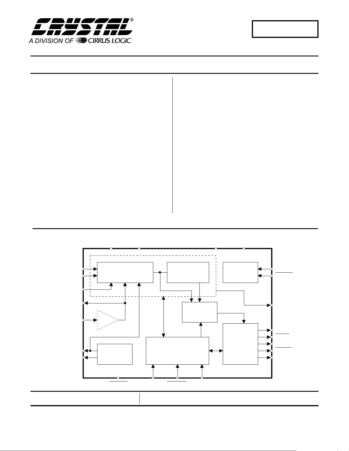
CS5181 is a fully calibrated high-speed ∆Σ analog-todigital converter, capable of 625 kSamp les/second output word rate (OWR). The OWR scales with the master
clock. It consists of a 5th order ∆Σ modulato r, decim ation
filter, and serial in terfac e. Th e chip c an use the 2.3 75 V
on-chip voltage reference, or an external 2.5 V refer-
ence. The input voltag e ra nge is 1.6 × VREFIN V
differential. Multip le CS518 1s can be ful ly sy nchroni zed
in multi-channel applications with a sync signal. The part
has a power-down m ode to minimize power c onsumption at times of system inacti vity. The hig h speed digital
I/O lines have complementary signals to help reduce radiated noise from traces on the PC board layout. The
CS5181 can also be operated in m odulator-only mode
which provides the del ta-sigma modulator bitstr eam as
the output.
ORDERING INFORMATION
CS5181-BL -40 °C to +85 °C 28-pin PLCC
VD+
DGND
pp
fully
AIN+
AIN-
∆Σ
Modulator
VREF-
VREF+
VREFIN
VREFOUT
VREFCAP
x1.6
Reference
PWDN SYNC RESET MODE
Preliminary Product Information
Cirrus Logic, Inc.
P.O. Box 17847, Austin, Texas 78760
(512) 445 7222 FAX: (512) 445 7581
http://www.crystal.com
Decimator Clock
Mode
MCLK
MCLK
MFLAG
Selector
SDO
Timing
and
Serial
Interface
Control
This document contains information for a new product.
Cirrus Logic reserves the right to modify this product without notice.
Copyright Cirrus Logic, Inc. 1999
(All Rights Reserved)
SDO
SCLK
SCLK
FSO
DS250PP1
APR ‘99
1

TABLE OF CONTENTS
CHARACTERISTICS/SPECIFICATIONS ................................................ ............4
ANALOG CHARACTERISTICS...................................................................4
DYNAMIC CHARACTERISTICS ................................................................. 5
DIGITAL CHARACTERISTICS....................................................................5
SWITCHING CHARACTERISTICS ........................................................ ..... 6
RECOMMENDED OPERATING CONDITIONS.......................................... 7
ABSOLUTE MAXIMUM RATINGS.............................................................. 7
GENERAL DESCRIPTION .................................................................................. 8
THEORY OF OPERATION .................................................................................. 8
Converter Initialization: Calibration and Synchronization ..........................8
Clock Generator ..........................................................................................9
Voltage Reference ......................................................................................9
Analog Input .............................................................................................10
Output Coding .......................................................................................... 10
Modulator-Only mode ............................................................................... 10
Instability Indicator .................................................................................... 12
Digital Filter Characteristics ...................................................................... 12
Serial Interface .......................................................................................... 12
Power Supplies / Board Layout ................................................................ 12
Power-down Mode .................................................................................... 14
PIN DESCRIPTIONS ......................................................................................... 15
PARAMETER DEFINITIONS ............................................................................. 18
APPENDIX A: CIRCUIT APPLICATIONS ......................................................... 20
PACKAGE OUTLINE DIMENSIONS ................................................................. 23
CS5181
Contacting Cirrus Logic Support
For a complete listing of Direct Sales, Distributor, and Sales Representative contacts, visit the Cirrus Logic web site at:
http://www.cirrus.com/corporate/contacts/
Preliminary product info rmation describes products which are i n p roduction, but for which ful l char act er iza t i on da t a is not yet available. Advance produ ct i nformation describes products which are in development and subject to development changes. Cirrus Logic, Inc. has made best efforts to ensure that the information
contained in this document is accurate and reli able. However , the i nformati on is sub ject to change with out no tice and i s provi ded “AS IS” withou t warranty of
any kind (express or implied). No responsibility is assumed by Cirrus Logic, Inc. for the use of this information, nor for infringements of patents or other rights
of third parties. This document i s the propert y of Cirru s Logic, Inc. and implie s no licen se under patent s, copyri ghts, trademarks, or tr ade secrets. No part of
this publication may be copied, reproduced , stored in a retrieval system, or transmitted, in any form or by any means (electronic, mechanical, photographic, or
otherwise) without the pri or wri tt en consen t of Ci rrus Logic, Inc. Items from any Cirrus Logic websi t e or di sk may be print ed for use by the user. However, no
part of the printout or electronic files may be copied, reproduced, stored in a retrieval system, or transmitted, in any form or by any means (electronic, mechanical,
photographic, or otherwise) without the prior written consent of Cirrus Logic, Inc.Furthermore, no part of this publication may be used as a basis for manufacture
or sale of any items without the prior written consent of Cirrus Logic, Inc. The names of products of Cirrus Logic, Inc. or other vendors and suppliers appearing
in this document may be trademarks or service marks of their respective owners which may be registered in some jurisdictions. A list of Cirrus Logic, Inc. trademarks and service marks can be found at http://www.cirrus.com.
2 DS250PP1

TABLE OF FIGURES
1. Serial Port Timing (not to scale) .............................................................................. 6
2. RESET and SYNC logic and timing. ....................................................................... 8
3. CS5181 connection diagram for using the internal voltage reference. .................... 9
4. CS5181 connection diagram for using an external voltage reference. .................. 10
5. Modulator Only Mode Data RTZ Format. .............................................................. 11
6. Circuit to Reconstruct
Return-to-Zero (RTZ) Data from SDO/SDO into Original Modulator Bitstream.... 11
7. Magnitude versus frequency spectrum of modulator bitstream
(MCLK = 40.0 MHz). .............................................................................................. 11
8. Expanded view of the magnitude versus frequency spectrum of modulator
bitstream (MCLK = 40 MHz). ................................................................................. 11
9. CS5181 Digital Filter Magnitude Response (MCLK = 40 MHz) ............................. 12
10. CS5181 Digital Filter Phase Response (MCLK = 40 MHz) ................................... 12
11. CS5181 System Connection Diagram ................................................................... 13
12. Single amplifier driving only AIN+, with AIN- held at a steady dc value ................ 20
13. Performance of amplifier of Figure 11 overdriving AIN+ input to the
CS5181 at 3.8 VPP ............................................................................................... 20
14. Performance of amplifier of Figure 11 with AIN+ driven at 2.0 VPP ...................... 20
15. Four amplifier balanced driver. .............................................................................. 21
16. Performance of amplifier in Figure 14 ................................................................... 21
17. Performance of amplifier in Figure 14 ................................................................... 22
18. CS5181 Differential Non-linearity plot. (Data taken with repeating ramp) ............ 22
19. Histogram of DNL from Figure 17 ......................................................................... 22
20. CS5181 Noise Histogram, 32768 samples. ......................................................... 22
CS5181
DS250PP1 3
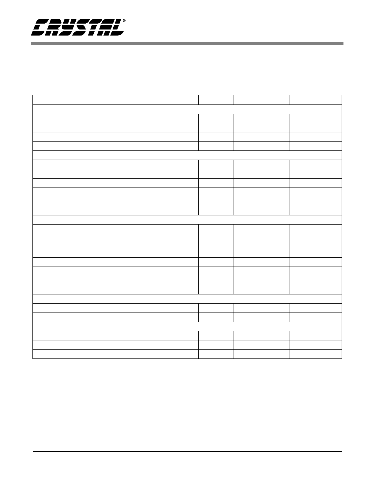
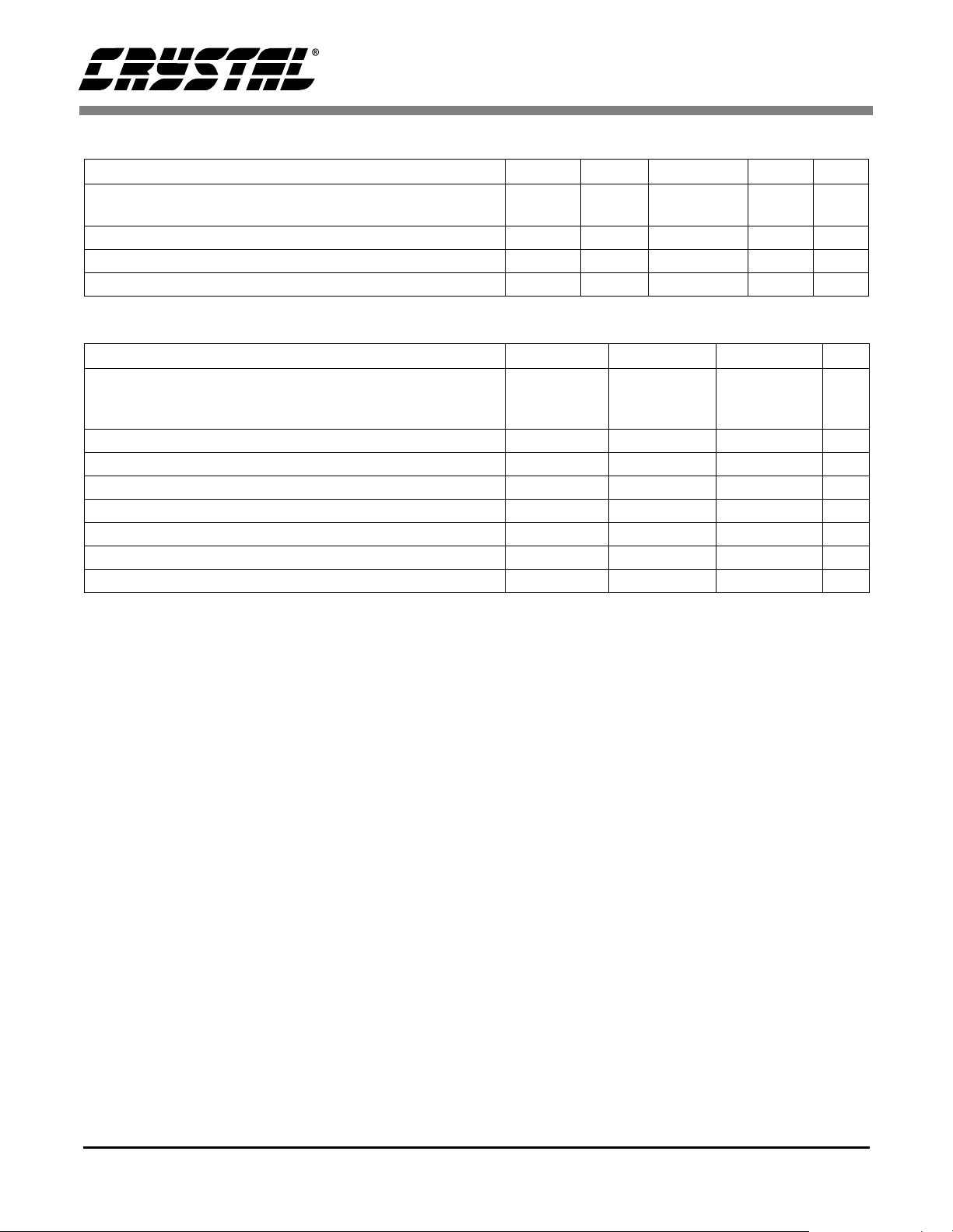
CHARACTERISTICS/SPECIFICATIONS
CS5181
ANALOG CHARACTERISTICS (T
DGND = 0 V; MCLK = 40.0 MHz; VREFIN = VREFOUT; MODE = VD+; Analog Source Impedance = 301 Ohms
with 2200 pF to AGND; Full-Scale input Sinewave at 22 kHz; Unless otherwise noted.)
Parameter Symbol Min Typ Max Unit
= -40 to 85 °C; VA+ = 5 V ±5%, VD+ = 3.3 V ±0.3V; AGND =
A
Dynamic Performance
Dynamic Range (Note 1) DR 89 93 - dB
Total Harmonic Distortion @ 22 kHz (Note 1) THD 84 89 - dB
Signal to (Noise + Distortion) SINAD 82 87 - dB
Spurious Free Dynamic Range SFDR 84 90 - dBc
Static Performance
Integral Nonlinear ity (Note 2) INL - ±2 - LSB
Differential Non-Linearity (Note 2) DNL - - ±0.5 LSB
Full Scale Error (Note 6) - ±8 - LSB
Full Scale Drift with Internal Reference (Notes 2 and 5) - ±50 - ppm/°C
Offset Error (Note 6) - ±8 - LSB
Offset Drift (Note 2) - ±6.0 - µV/°C
Analog Input
Differential Input Voltage Range (Note 3) - 1.6 X
VREFIN
Common Mode Range CMR 1 - VREFIN
Input Capacitance - 4.0 - pF
Differential Input Impedance (capacitive) - 300 - k
Common Mode Rejection Ratio (Note 2) CMRR 50 - - dB
Common Mode Input Current - ±160 ±320 µA
-V
+ 0.25
pp
V
Ω
Reference Input
VREFIN 2.25 2.375 2.6 V
VREFIN Current (Note 4) - 1 ±320 µA
Reference Output
VREFOUT Voltage 2.25 2.375 2.5 V
VREFOUT Output Current - - ±500 µA
VREFOUT Impedance - 0.1 -
Ω
Notes: 1. Dynamic range is tested with a 22 kHz input signal 60 dB below full scale.
2. Specification guaranteed by design, characterization, and/or test.
3. Full scale fully-differential input span is nominally 1.6 X the VREFIN voltage. The peak negative
excursion of the signals at AIN+ or AIN- should not go below AGND for proper operation.
4. VREFIN current is less than 1 µA unde r normal operation, but can b e as high a s ± 320 µA durin g calibratio n.
5. Drift of the on-chip reference alone is typically about ±30 ppm/°C. If using an external reference, total
full scale drift will be that of the external reference plus an additional ±20 ppm/°C, which is the typical
drift of the X1.6 buffer.
6. Applies after self-calibration at final operating ambient temperature.
4 DS250PP1
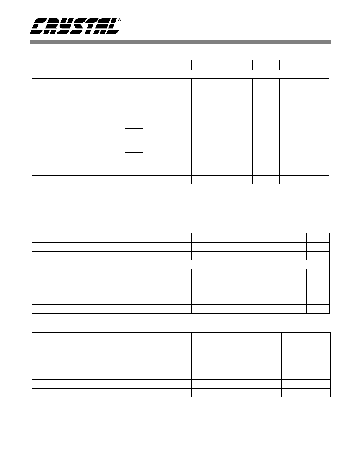
ANALOG CHARACTERISTICS (Continued)
Parameter Symbol Min Typ Max Unit
Power Supplies
Power Supply Current (MODE = 1, PWDN = 1) (Note 7)
VA1+, VA2+ = 5 V
VD1+, VD2+ = 3.3 V
CS5181
-
-
53
92.4
65
100
mA
mA
Power Supply Current (MODE = 1, PWDN
VA1+, VA2+ = 5 V
VD1+, VD2+ = 3.3 V
Power Supply Current (MODE = 0, PWDN
VA1+, VA2+ = 5 V
VD1+, VD2+ = 3.3 V
Power Supply Current (MODE = 0, PWDN
VA1+, VA2+ = 5 V
VD1+, VD2+ = 3.3 V
Power Supply Rejection (Note 9) PSRR - 55 - dB
Notes: 7. All outputs unloaded. All inputs except MCLK held static at VD+ or DGND.
8. Power consumpti on whe n PWDN
9. Measured with a 100 mV
= 0) (Notes 7, 8)
= 1) (Note 7)
= 0) (Notes 7, 8)
= 0 applies only for no master clock applied (MCLK held high or low).
sine wave on the VA+ supplies at a frequency of 100 Hz.
pp
-
-
-
-
-
-
3.7
0.062
53
18.9
3.7
0.062
6
0.2
65
22
6
0.2
mA
mA
mA
mA
mA
mA
DYNAMIC CHARACTERISTICS
Parameter Symbol Min Typ Max Unit
Modulator Sampling Frequency - MCLK - Hz
Output Word Rate - MCLK/64 - Hz
Filter Characteristics (Note 2)
-3 dB Corner - MCLK/142.3804 - Hz
Passband Ripple - - ±0.05 dB
Stopband Frequency - MCLK/128 - Hz
Stopband Rejection 90 - - dB
Group Delay - 2370/MCLK - s
DIGITAL CHARACTERISTICS
Parameter Symbol Min Typ Max Unit
High-Level Input Voltage V
Low-Level Input Voltage V
High-Level Output Voltage (I
Low-Level Output Voltage (I
Input Leakage Current I
Input Capacitance Cin - 6 - pF
DS250PP1 5
= -100 µA) V
O
= 100 µA) V
O
Specifications are subject to change without notice.
(TA = -40 to 85 °C; VD = 3.3V ±0.3V; AGND = DGND = 0 V)
IH
IL
OH
OL
in
2.0 - - V
--0.8V
2.7 - - V
--0.3V
-±1±10µA
CS5181
SWITCHING CHARACTERISTICS (T
= -40 to 85 °C; VA+ = 5 V ±5%, VD+ = 3.3 V ±0.3 V;
A
AGND = DGND = 0 V; MODE = VD+)
Parameter Symbol Min Typ Max Unit
Master Clock Frequency (Note 2) MCLK 0.512 25 to 40 41 MHz
Master Clock Duty Cycle 45 - 55 %
Rise Times (Notes 2, 10, and 11)
Any Digital Input, Except MCLK
MCLK
Any Digital Output
Fall Times (Notes 2, 10, and 11)
Any Digital Input, Except MCLK
MCLK
Any Digital Output
t
t
rise
fall
-
-
-
-
-
-
20
20
-
-
-
-
100
.2/MCLK
-
100
.2/MCLK
-
ns
s
ns
ns
s
ns
Calibration/Sync
RESET rising to MCLK rising
RESET
rising recognized, to FSO falling
-3 -ns
- 988205/MCLK - s
SYNC rising to MCLK rising - 3 - ns
SYNC rising recognized to FSO falling - 5161/MCLK - s
PWDN
rising recognized to FSO falling
SYNC high time
RESET
low time
- 5168/MCLK - s
1/MCLK - - s
1/MCLK - - s
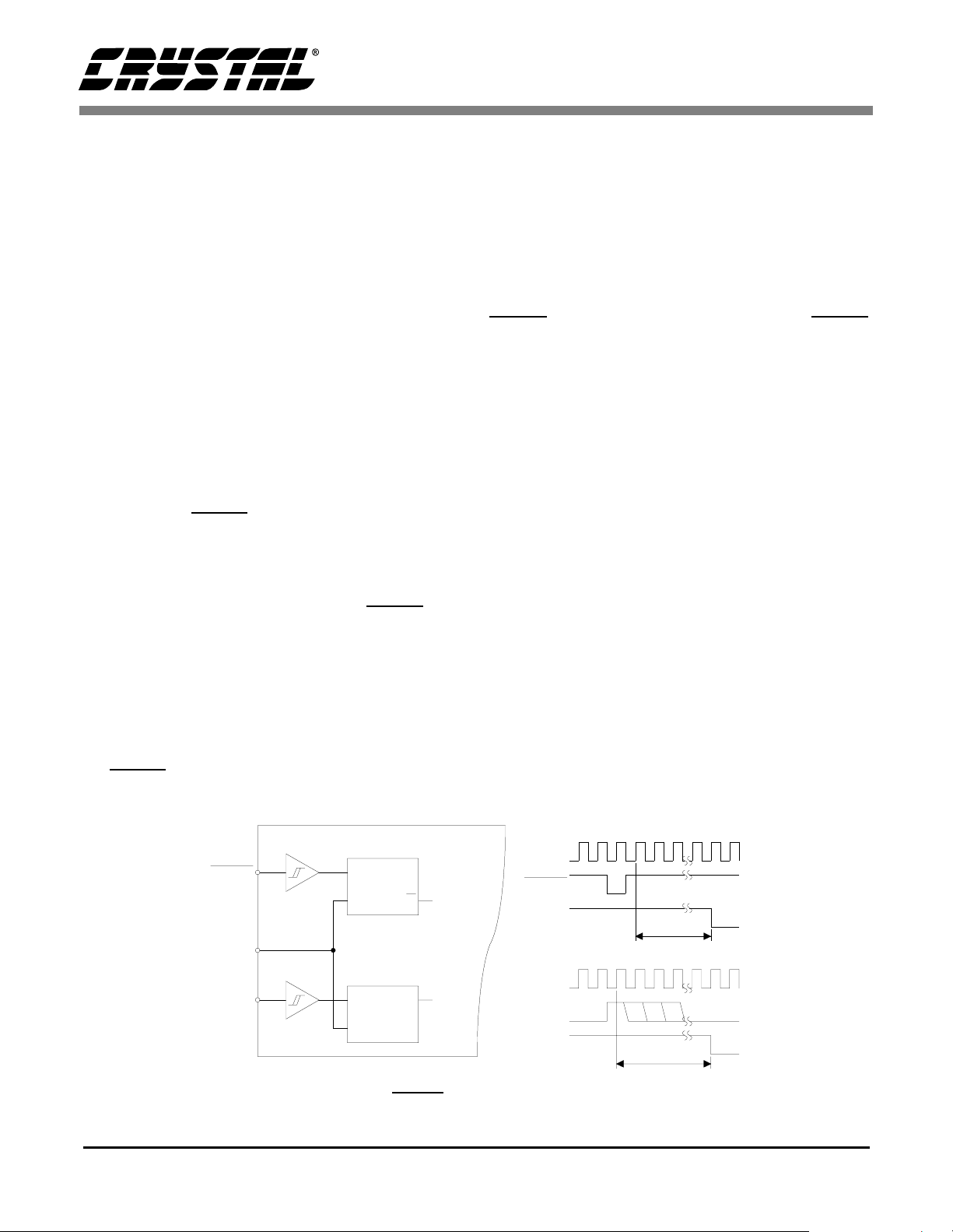
Serial Port Timing (Note 12)
SCLK frequency - MCLK/3 - Hz
SCLK high time t
SCLK low time t
FSO falling to SCLK rising t
SCLK falling to new data bit t
SCLK rising to FSO rising t
1
2
3
4
5
-1/MCLK-s
-2/MCLK-s
-2/MCLK+2E-9 - s
-1.5 -ns
-1/MCLK-2E-9 - s
Notes: 10. Rise and Fall times are specified at 10% to 90% points on waveform.
11. RESET
12. Specifications applicable to complementary signals SCLK
, SYNC, and PWDN have Schmitt-trigger inputs.
FSO
t1t
2
SCLK
SDATA
t
3
t
4
XX
MSB MSB-1 LSB-1 LSB
and SDO.
t
5
XX
Figure 1. Serial Port Timing (not to scale)
6 DS250PP1
CS5181
RECOMMENDED OPERATING CONDITIONS (AGND = DGND = 0 V)
Parameter Symbol Min Typ Max Unit
DC Power Supplies Digital
Analog
Analog Reference Voltage VREFIN 2.25 2.5 2.6 V
AGND to DGND differential -100 0 100 mV
Operating Junction Temperature T
ABSOLUTE MAXIMUM RATINGS
Parameter Symbol Min Max Unit
DC Power Supplies Ground
Digital
Analog
Input Current, Any pin except Supplies I
Output Current I
Power Dissipation (Total) - 1000 mW
Analog Input Voltage V
Digital Input Voltage V
Ambient Operating Temperature T
Storage Temperature T
VD+
VA+
j
AGND/DGND
VD+
VA+
in
out
INA
IND
A
stg
3.0
4.75
3.3
5
3.6
5.25
--120°C
-0.3
-0.3
-0.3
(VD+) + 0.3
6.0
6.0
-±10mA
-±25mA
-0.3 (VA+) + 0.3 V
-0.3 (VD+) + 0.3 V
-40 85 °C
-65 150 °C
V
V
V
V
V
WARNING: Operation beyond these limits may result in permanent damage to the device. Normal operation is not
guaranteed at these extremes.
Specifications are subject to change without notice.
DS250PP1 7
CS5181
GENERAL DESCRIPTION
The CS5181 is a monolithic CMOS 16-bit A/D
converter designed to operate in continuous mode
after being reset.
The CS5181 can operate in modulator-only mode
in which the bit stream from the modulator is the
data output from the device.
THEORY OF OPERATION
The front page of this data sheet illustrates the
block diagram of the CS5181.
Converter Initialization: Calibration and Synchronization
The CS5181 does not have an internal power-on reset circuit. Therefore when power is first applied to
the device the RESET pin should be held low until
power is established. This resets the converter’s logic to a known state. When power is fully established
the converter will perform a self-calibration, starting
with the first MCLK rising edge after RESET goes
high. The converter will use 988,205 MCLK cycles
to complete the calibration and to allow the digital
filter to fully settle, after which, it will output fullysettled conversion words. The converter will then
continue to output conversion words at an output
word rate equal to MCLK/64. Figure 2 illustrates
the RESET and SYNC logic and timing for the converter.
The CS5181 is designed to perform conversions
continuously with an output rate that is equivalent
to MCLK/64. The conversions are performed and
the serial port is updated independent of external
controls. The converter is designed to measure differential bipolar input signals, and unipolar signals,
with a common mode voltage of between 1.0 V and
VREF + 0.25 V. Calibration is performed when the
RESET signal to the device is released. If RESET
is properly framed to MCLK, the converter can be
synchronized to a specific MCLK cycle at the system level.
The SYNC signal can also be used to synchronize
multiple converters in a system. When SYNC is
used, the converter does not perform calibration.
The SYNC signal is recognized on the first rising
edge of MCLK after SYNC goes high. SYNC
aligns the output conversion to occur every 64
MCLK clock cycles after the SYNC signal is recognized and the filter is settled. After the SYNC is
initiated by going high, the converter will wait
5,161 MCLK cycles for the digital filter to settle
before putting out a fully-settled conversion word.
To synchronize multiple converters in a system, the
SYNC pulse should rise on a falling edge of the
MCLK signal. This ensures that the SYNC input to
all CS5181s in the system will be recognized on the
next rising edge of MCLK. Use of the SYNC input
CS5181
RESET
MCLK
SYNC
8 DS250PP1
D
CLK
D
CLK
Figure 2. RESET and SYNC logic and timing.
Q
Q RESET
QSYNC
MCLK
RESET
FSO
988205 MCLK Cycles
MCLK
SYNC
FSO
5161 MCLK Cycles

CS5181
is not necessary to make the converter operate
properly. If it is unused it should be tied to DGND.
Conversion data is output from the SDO and SDO
pins of the device. The data is output from the SDO
pin MSB first, in two’s complement format. The
converter furnishes a serial clock SCLK and its
complement SCLK to latch the data bits; a nd a data
frame signal, Frame Signal Output (FSO), which
frames the output conversion word. The SCLK
output frequency is MCLK/3.
Clock Generator
The CS5181 must be driven from a CMOS-compatible clock at its MCLK pin. The MCLK input is
powered from the VD+ supply and its signal input
should not exceed this supply. The required
MCLK is 64 × OWR (Output Word Rate). To
achieve an Output Word Rate of 625 kHz, the
MCLK frequency must be 64 × 625 kHz, or
40 MHz. A second clock input pin, MCLK, is not
actually used inside the device but allows the user
to run a fully differential clock to the converter to
minimize radiated noise from the PC board layout.
The CS5181 can be operated with MCLK frequencies from 512 kHz up to 40 MHz. The output word
rate scales with the MCLK rate with
OWR = MCLK/64.
Voltage Reference
The CS5181 can be configured to operate from either its internal voltage reference, or from an external voltage reference.
The on-chip voltage reference is nominally 2.375V
and is referenced to the AGND pins. This 2.375 V
reference is output from the VREFOUT pin. It is
then filtered and returned to the VREFIN pin. The
VREFIN pin is connected to a buffer which has a
typical gain of 1.6. This scales the on-chip reference
of 2.375 V to 3.8 V. This value sets the peak-to-peak
input voltage into the AIN pins of the converter. Figure 3 illustrates the CS5181 connected to use the internal voltage reference. Note that a 1.0 µF and 0.1
µF capacitor are shown connected to the VREFCAP
pin to filter out noise. A larger capacitor can be used,
but may require a longer reset period when first powering up the part to allow for the reference to stabilize
before the part self-calibrates.
Alternatively, the CS5181 can be configured to use
an external voltage reference. Figure 4 illustrates
the CS5181 connected to use a 2.5 V e xternal reference. In this case, the maximum peak-to-peak
signal input at the AIN pins is 4.0 V.
CS5181
VREFIN
VREF +
10 µF 0.1 µF
+
+
10 µF 0.1 µF
+
1 µF 0.1 µF
Figure 3. CS5181 connection diagram for using the internal voltage reference.
DS250PP1 9
VREF-
VREFOUT
VREFCAP
X1.6
Modulator
X1
Reference

CS5181
VS
+
10 µF 0.1 µF
Figure 4. CS5181 connection diagram for using an external voltage reference.
2.5 V
10 µF
0.1 µF
+
10 µF 0.1 µF
10 µF 0.1 µF
1 µF 0.1 µF
Analog Input
The analog signal to the converter is input into the
AIN+ and AIN- pins. The input signal is fully differential with the maximum peak-to-peak amplitude of VREFIN X 1.6 V. The signal needs to have
a common mode voltage in a range from 1.0 V to
VREF + 0.25 V for minimum distortion. A resistor-capacitor filter should be included on the AIN+
and AIN- inputs of the converter. This should consist of a 20 Ω resistor and a 2200 pF ca pacitor on
each input to ground as illustrated in the system
connection diagram (Figure 11).
Output Coding
Table 1 illustrates the output coding for the converter when operating with the digital filter
(MODE = 1). The converter outputs its data from
the serial port in twos complement format, MSB
first.
The chip offers an MFLAG signal to indicate when
the modulator has gone unstable. MFLAG is set
when an overrange signal forces the modulator into
an unstable condition. Under this condition, output
CS5181
VREFIN
VREF+
+
VREF-
VREFOUT
+
VREFCAP
+
Fully Differential Bipolar
Input Voltage
- 1.5 LSB) 7FFF
>(V
FS
VFS - 1.5 LSB
-0.5 LSB
-VFS + 0.5 LSB
<(-VFS + 0.5 LSB) 8000
Notes: 1. V
X1.6
Modulator
X1
Reference
1
= VREFIN x 1.6
FS
Table 1. Output Coding.
Twos Complement
7FFF
7FFE
0000
FFFF
8001
8000
codes from the converter will be locked to either
plus or minus full scale as is appropriate for the
overrange condition.
Modulator-Only mode
The CS5181 can be operated in modulator-only
mode by connecting the MODE pin to a logic 0
(DGND).
In modulator-only mode the noise-shaped bitstream from the fifth-order delta-sigma modulator
is output from the SDO and SDO (inverse bitstream) pins.
10 DS250PP1

MCLK
Figure 6. Circuit to Reconstruct
Return-to-Zero (RTZ) Data from
SDO/SDO
into Original Modulator Bitstream.
Modulator
Data
SDO
SDO
CS5181
Reconstructed
Data
Figure 5. Modulator Only Mode Data RTZ Format.
The data from the modulator is output from
SDO/SDO in RTZ (Return to Ze ro) format. The
circuit in Figure 6 can be used to reconstruct the
data so it can be captured with the rising or falling
edge of MCLK.
Table 2 illustrates the magnitude of the input signal
into the chip versus the ones density out of the
modulator. The table does not take into account the
potential offset and gain errors of the modulator
and their effect on the ones density.
Fully Differential Bipolar
Input Voltage
V
FS
050%
-V
Notes: 2. V
3. Ones density is approximate; it does not
take offset and gain errors into
consideration.
Table 2. Modulator-Only Mode Ones Density.
2
FS
= VREFIN x 1.6
FS
Modulator Ones
Density
3
75%
25%
Figure 7 and Figure 8 illustrate magnitude versus
frequency plots of the modulator bitstream when
running at 40.0 MHz.
Figure 7. Magnitude versus frequency spectrum of
modulator bitstream
(MCLK = 40.0 MHz).
SDO
SDO
DS250PP1 11
Reconstructed
Data
Reconstructed
Data
Figure 8. Expanded view of the magnitude versus fre-
quency spectrum of modulator bitstream
(MCLK = 40 MHz).

Instability Indicator
The MFLAG signal is functional in both modes of
operation of the part and indicates when the modulator has been overdriven into an unstable condition. In the modulator only mode (MODE = 0), the
MFLAG signal will remain set for 3 M CLK cycle s
when the modulator goes unstable, before being returned to the reset state. While the input condition
causing modulator instability persists, the MFLAG
signal will continually get set for 3 MCLK cycles
and then get reset.
CS5181
When the decimation filter on the p art is operational (MODE = 1), the MFLAG signal is set when the
modulator goes unstable. In this mode, however,
the MFLAG signal stays set until 5,120 MCLK cycles after the input condition causing modulator instablility is removed. This delay is provided to
allow the digital filter time to settle, and the part
will output fully settled conversion words after the
MFLAG signal goes low.
Digital Filter Characteristics
Figure 9 illustrates the magnitude versus frequency
plot of the converter when operating at a 625 kHz
output word rate. The filter is a non-aliasing 4265
tap filter with a -3 dB corner at 0.4495 of the output
word rate and an out-of-band attenuation of at least
90 dB at frequencies above one half the output
word rate. The passband ripple is less than
±0.05 dB up to the -3 dB corner frequency.
Figure 10 illustrates the phase response of the digital filter with the converter operating at 625 kHz
output word rate. The filter characteristics change
proportional to changes in the MCLK rate.
The group delay of the digital filter is 2370 MCLK
cycles (59.3 µs with MCLK = 40 MHz), and the
settling time is 4740 MCLK cycles (118.5 µs).
Figure 9. CS5181 Digital Filter Magnitude Response
(MCLK = 40 MHz)
250.00
200.00
150.00
100.00
50.00
0.00
Phase (deg.)
-50.00
-100.00
-150.00
-200.00
-250.00
0 50k 100k 150k 200k 250k 300k
Freq (Hz)
Figure 10. CS5181 Digital Filter Phase Response
(MCLK = 40 MHz)
rial Data Output pin (SDO), and its complement
(SDO); Serial Clock (SCLK), and its complement
(SCLK); and the Frame Sync Output (FSO). FSO
falls at the beginning of an output word. Data is
output in twos complement format, MSB first.
FSO stays low for 16 SCLK cycles. SCLK is output at a rate equal to MCLK/3.
Serial Interface
The CS5181 has a serial interface through which
conversion words are output in a synchronous selfclocking format. The serial port consists of the Se-
12 DS250PP1
Power Supplies / Board Layout
The CS5181 requires an analog supply voltage of
5.0 Volts and a digital supply voltage of 3.3 Volts
(nominal) for proper operation.

CS5181
Figure 11 illustrates the system connection diagram
for the chip. For best performance, each of the
supply pins should be bypassed to the nearest
ground pin on the chip. The bypass capacitors
should be located as close to the chip as possible. If
the chip is surface mounted the bypass capacitors
should be on the same side of the circuit card as the
chip.
The CS5181 is a high speed component that requires adherence to standard high-frequency printed circuit board layout techniques to maintain
optimum performance. These include the use of
ground and power planes, using low noise power
1
AGND1
+5 V
0.1 µF
28
VA1+
supplies in conjunction with proper supply decoupling, minimizing circuit trace lengths, and physical separation of digital and analog components
and circuit traces.
It is preferred that any clock oscillator circuitry be
located on a ground plane separate from the digital
plane in order to ensure that digital noise does not
induce clock jitter.
For additional insight, see the CDB5181 evaluation
board for more details. Also refer to Application
Note AN18 which covers layout and design rules
for high resolution data converters.
DGND1
VD1+
22
21
0.1 µF
+3.3 V
8
VA2+
0.1 µF
+
10 µF
+
10 µF
+
1 µF
20
3.8 V Fully
pp
Differential
CMV = 2.375 V
The 3.8 V fully differential input span is set by the converter’s internal voltage reference at 2.375 V.
An input span of 4.0 V fully differential would result if an external voltage reference of 2.5 V is used.
~
20
pp
0.1 µF
0.1 µF
0.1 µF
Ω
2200 pF
Ω
2200 pF
pp
7
18
4
5
3
2
6
26
27
AGND2
AGND3
VREFOUT
VREFIN
VREF-
VREF+
VREFCAP
AIN+
AIN-
CS5181
VD2+
DGND2
PWDN
MODE
RESET
SYNC
MFLAG
MCLK
MCLK
SCLK
SCLK
FSO
SDO
SDO
12
11
25
24
23
10
9
20
19
17
14
13
16
15
0.1 µF
Control
Source
Interface
Logic
Clock
Data
Figure 11. CS5181 System Connection Diagram
DS250PP1 13

CS5181
Power-down Mode
The CS5181 has a PWDN (power-down) function.
When active low, power to most of the converter’s
circuitry will be reduced. If MCLK is to be stopped
to save power, it should not be stopped until at least
ten clock cycles after PWDN is taken low. The ten
clock cycles are required to allow the part to turn
off it’s internal circuitry. If the part does not get the
full ten clock cycles, it will still go into a power
down state, but the power dissipation could be
more than is listed in the specifications for the full
power down condition. When PWDN is active, the
calibration information inside of the converter is
maintained. When coming out of the power-down
state, the converter is not recalibrated and will
start-up similar to when SYNC is initiated.
14 DS250PP1
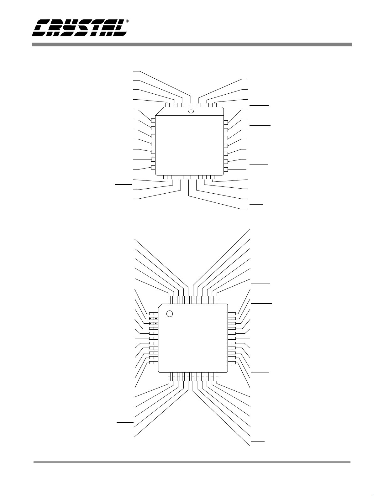
PIN DESCRIPTIONS
Analog Ground AGND
Pos. Reference VREF+ VA1+ Positive Analog Supply
Neg. Reference VREF- AIN- Negative Analog Input
Referenc e Output VREFOUT AIN+ Positive Analog Input
Pos. Reference Input VREFIN PWDN
Referenc e Bypass VREFCAP MODE Modulator Only Mode
Analog Ground AGND RE SET
Analog Supply VA2+ DGND Digital Ground
Invalid Conversion MFLAG VD1+ Positive Digital Supply
Sync. Filter SYNC MCLK Master Clock
Digital Ground DGND MCLK
5
6
7
8
9
10
11
12 13 14 15 16 17
1234282726
CS5181
18
25
24
23
22
21
20
19
Pos. Digital Supply VD2+ AGND Analog Ground
Inverse Serial Clock SCLK
FSO Frame Sync Output
Serial Clock SCLK SDO Serial Data Out
SDO
Power Down Mode
Reset and Calibration
Inverse Master Clock
Inverse Serial Data Out\
CS5181
AGND Analog Ground
Analog Ground AGND V A1+ Positive Analog Supply
Pos. Reference VREF+ AGND Analog Ground
Neg. Reference VREF- AIN- Negative Analog Input
Reference Output VREFOUT AIN+ Positive Analog Input
Analog Ground AGND AGND Analog Ground
Analog Ground AGND PWDN
Power Down Mode
Reference Input VREFIN MODE Modulator Only Mode
Reference Bypass VREFCAP RESET
Analog Ground AGND DGND Digital Ground
Analog Ground AGND DGND Digital Ground
Analog Supply VA2+ VD1+ Positive Digital Supply
Analog Supply VA2+ VD1+ Positive Digital Supply
Invalid Conversion MFLAG DGND Digital Ground
Sync. Filter SYNC MCLK Master Clock
4443424140393837363534
1
2
3
4
5
6
7
8
9
10
11
CS5181
1213141516171819202122
33
32
31
30
29
28
27
26
25
24
23
Digital Ground DGND MCLK
Reset and Calibration
Inverse Master Clock
Digital Ground DGND DGND Digital Ground
Pos. Digital Supply VD2+ NC
Pos. Digital Supply VD2+ AGND Analog Ground
Digital Ground DGND NC
Inverse Serial Clock SCLK
FSO Frame Sync Output
Serial Clock SCLK SDO Serial Data Out
SDO
Inverse Serial Data Out\
DS250PP1 15

Supply Inputs
VA1+, VA2+ — Positive Analog Supply
Input for the positive analog supply is +5.0 V typical when AGND is 0 V.
AGND — Analog Ground
Analog ground for circuits supplied by VA+.
VD1+, VD2+ — Positive Digital Supply
Input for positive digital supply is +3.3 V typical when DGND is 0 V.
DGND — Digital Ground
Digital ground for circuits supplied by VD+.
Signal and Reference Related Inputs
AIN+, AIN- — Differential Analog Inputs
CS5181
Fully differential signal inputs.
VREFIN — Voltage Reference Input
VREFOUT or an external reference is connected to VREFIN. Analog input voltage (full scale
fully differential peak-to-peak) into the converter is 1.6 times this value.
VREF+ — Positive Voltage Reference
Filter capacitor connection for the reference input buffer. The voltage on this pin equals
VREFIN X 1.6.
VREF- — Negative Voltage Re ference
VREF- is connected to AGND.
VREFOUT — Voltage Refe rence Output
Output pin for the 2.375 volt on-chip reference relative to AGND.
VREFCAP — Reference Bypass
Filter capacitor connection for internal reference.
Serial Interface I/O Signals
SCLK, SCLK — S erial Interface Clock
Serial Clock Output. A gated serial clock output from the converter at a rate equal to 1/3 the
MCLK clock rate. The SCLK output is a complement of SCLK and helps reduce radiated
noise if the two lines are run adjacent on the PC board layout and drive a balanced load.
16 DS250PP1

SDO, SDO — Serial Data Out
Serial Data Output. Output pin for 16-bit serial data word. The SDO output is the complement
of SDO and helps to reduce radiated noise if the two lines are run adjacent on the PC board
layout. Output data is output in twos complement format MSB first.
FSO — Frame Sync Output
Frame Sync Output. The Frame Sync Output turns low to indicate the beginning of an output
word from the SDO pin. It returns high after the 16 data bits have been clocked out.
Control Pins
RESET — Reset and Calibration
When the RESET pin is pulled to a logic low the converter will perform a reset of its digital
logic. When the level on this pin is brought back to a logic high the chip starts normal
operation, following a two clock cycle delay period. When MODE = 1, the chip goes through
an internal gain and offset calibration routine following this reset sequence.
CS5181
PWDN — Power Down Mode
A logic 0 on the PWDN pin will put the device into a power-down mode.
MODE — Modulator Only Mode
MODE is held at a logic high for normal operation. In normal operation the device utilizes the
digital decimation filter and calibration ciruitry. MODE = 0 puts the part in modulator only
mode whereby most of the digital circuitry is powered-down and the modulator bit-stream is
output from the SDO and SDO pins.
SYNC — Synchronization of Filter
The SYNC input can be used to restart the digital filter of the converter at the beginning of its
convolution cycle. The SYNC input is used to synchronize the filters of multiple converters in
a system. When the SYNC signal goes high, the filter will be initialized and will begin its
convolution cycle on the next rising edge of MCLK. If not used, tie SYNC to DGND.
MFLAG — Invalid Conversion Flag
MFLAG goes high if the modulator portion of the converter goes unstable. If MFLAG is high,
the output data from the converter may be invalid.
MCLK, MCLK — Master Clock Signal
Master clock input accepts a CMOS level clock input to the converter with worst case duty
cycle of 45-55% (typically 40 MHz). MCLK is not actually used inside the device, but can be
used for radiated noise cancellation if MCLK and MCLK are run adjac ent to each other on the
PC board.
DS250PP1 17

PARAMETER DEFINITIONS
Differential Non-Linearity Error - DNL
The deviation of a code’s width from ideal. Units in LSBs.
Integral Non-Linearity Error - INL
The deviation of a code from a straight line passing through the endpoints of the transfer
function after zero- and full-scale errors have been accounted for. "Zero-scale" is a point 1/2
LSB below the first code transition and "full-scale" is a point 1/2 LSB beyond the code
transition to all ones. The deviation is measured from the middle of each particular code. Units
in LSB’s.
Full-Scale Error - FSEP
The deviation of the last code transition from the ideal (VREF-3/2 LSB’s). Units in LSB’s.
Offset Error - VOS
The deviation of the mid-scale transition from the ideal (1/2 LSB below 0 Volts). Units in
LSB’s.
CS5181
Spurious-Free-Dynami c-Range - SFDR
The ratio of the rms value of the full-scale signal, to the rms value of the next largest spectral
component (excepting dc). This component is often an aliased harmonic when the signal
frequency is a significant proportion of the sampling rate. Units in dBc (decibels relative to the
carrier).
Total Harmonic Distortion - THD
The ratio of the rms sum of the significant harmonics (2nd thru 7th), to the rms value of the
full-scale signal. Units in decibels.
Dynamic Range - DR
The ratio of the rms value of the inferred full-scale signal, to the rms sum of the broadband
noise signals below the Nyquist rate (excepting dc and distortion terms). Expressed in
decibels. Dynamic Range is tested with a 22 kHz input signal 60 dB below full scale. 60 dB
is then added to the resulting number to refer the noise level to the full-scale signal. This
technique ensures that the distortion components are below the noise level and do not affect the
measurement.
Signal-to-Noise-and-Distortion (s/[n+d]) - SINAD
The ratio of the rms value of the full-scale signal, to the rms sum of all other spectral
components below the Nyquist rate (excepting dc), including distortion components. Expressed
in decibels.
Group Delay
The time delay through the digital filter section of the part. Units in seconds.
18 DS250PP1

Resolution - N
The number of different output codes possible. Expressed as N, where 2N is the number of
available output codes.
Noise -
A measure of the variability of the converter’s output when a fixed DC input (usually ground)
is applied to the input and a large number of samples are taken. RMS noise is determined
statistically as the Standard Deviation of the Probability Density Function derived from the
histogram of the ADC with the differential inputs shorted together and tied to an appropriate
common mode voltage.
Common Mode Rejection Ratio - CMRR
A measure of the device’s ability to cancel out the effect of a common voltage applied to both
of its differential inputs. CMRR is specified as the ratio of the differential signal gain to the
gain for the common-mode signal. Units in dB.
Offset Drift -
Changes in the offset error of the part after self calibration due to changes in ambient
temperature. Specified in microvolts per degree C, relative to the input signal.
CS5181
Full Scale Drift -
Changes in the full scale error of the part after self calibration due to changes in ambient
temperature. Specified in parts-per-million (PPM) of the full scale range per degree C.
DS250PP1 19

APPENDIX A: CIRCUIT APPLICATIONS
Several amplifier circuits have been te sted with t he
CS5181. Performance at higher frequencies is generally limited by the operational amplifiers used to
drive the A/D converter.
Figure 12 illustrates a single operational amplifier
circuit which can accept a single-ended ground-referenced signal and condition it for the input of the
CS5181. The amplifier is AC-coupled to the signal
source. In this circuit the AIN- input to the CS5181
is held at a constant DC value and the AIN+ input
is driven (it is actually overdriven to achieve high
dynamic range, but this sacrifices performance
with regard to distortion). The common mode voltage for the CS5181 input should be designed to
stay between 1 V and VREF + 0.25 V when driven
at its AIN+ and AIN- inputs. The single amplifier
circuit in figure 12 has the disadvantages that the
common mode restriction limits the input signal
range and also causes errors due to variation in the
common mode voltage, as opposed to applying a
balanced differential signal.
CS5181
Figure 13. Performance of amplifier of Figure 12 over-
driving AIN+ input to the CS5181 at 3.8 V
Test Signal: 30.14 kHz @ -6 dB
S/N = 85.46 dB
S/D = 71.25 dB
S/N+D = 71.09 dB
8192 Samples
PP
Figures 13 and 14 illustrate the performance of the
amplifier of Figure 12 operating with a 3.8 Vpp input into the AIN+ input; and with 2.0 Vpp input into
the AIN+ input respectively.
+15
0.1 µF
0.15
C0G
+
Ω
10 k
10 k
5 k
Figure 12. Single amplifier driving only AIN+, with AIN- held at a steady dc value
U1
+
Ω
Ω
-15
1 k
10 µF
++
Figure 14. Performance of amplifier of Figure 12 with
Ω
0.1 µF
20
Ω
2200 pF
20
Ω
2200 pF
AIN+ driven at 2.0 V
AIN+
CS5181
AIN-
VREFOUT
10 µF0.1 µF
PP
20 DS250PP1

2 k
CS5181
Ω
10 k
2 k
+15 V
0.1 µF
-
U1
+
Ω
-15 V
2 k
Ω
+15 V
Ω
-
+
U2
-15 V
0.1 µF
0.1 µF
0.1 µF
2 k
10 k
2 k
Ω
Ω
Ω
-
+
-15
+15 V
-
+
+15 V
U3
2 k
U4
-15 V
10 µF
0.1 µF
0.1 µF
Ω
0.1 µF
+
2200 pF
2200 pF
0.1 µF
301
301
10 k
Ω
AIN-
CS5181
Ω
100
Ω
AIN+
Ω
VREFOUT
Figure 15. Four amplifier balanced driver.
Figure 15 illustrates a four amplifier circuit which
gives the best performance by keeping everything
balanced. Performance is generally limite d by the
amplifiers. Again, the output resistors are used to
scale down the input signal. Figures 16 and 17 illustrate the performance of the CS5181 with this
amplifier circuit.
Figure 18 illustrates a Differential Non-linearity
plot of the converter. Data for the plot was taken
using a repeating ramp. Figure 19 is a histogram of
the DNL data in Figure 18.
Figure 20 illustrates a noise histogram of the converter with its inputs shorted and connected to a
proper common mode voltage.
Test Sign al: 20 kHz @ 0 dB
S/N = 93.2 dB
S/D = 88.6 dB
S/N+D = 87.2 dB
8192 Samples
Figure 16. Performance of amplifier in Figure 15
DS250PP1 21

CS5181
Test Signal: 60 kHz @ 0 dB
S/N = 92.0 dB
S/D = 85.9 dB
S/N+D = 85.0 dB
8192 Samples
Figure 17. Performance of amplifier in Figure 15 Figure 18. CS5181 Differential Non-linearity plot. (Data
taken with repeating ramp)
Figure 19. Histogram of DNL from Figure 18 Figure 20. CS5181 Noise Histogram, 32768 samples.
22 DS250PP1

PACKAGE OUTLINE DIMENSIONS
28L PLCC PACKAGE DRAWING
CS5181
e
D2/E2
B
D1
D
E1 E
A1
A
INCHES MILLIMETERS
DIM MIN MAX MIN MAX
A 0.165 0.180 4.043 4.572
A1 0.090 0.120 2.205 3.048
B 0.013 0.021 0.319 0.533
D 0.485 0.495 11.883 12.573
D1 0.450 0.456 11.025 11.582
D2 0.390 0.430 9.555 10.922
E 0.485 0.495 11.883 12.573
E1 0.450 0.456 11.025 11.582
E2 0.390 0.430 9.555 10.922
e 0.040 0.060 0.980 1.524
JEDEC # : MS-018
DS250PP1 23

 Loading...