

Datasheet CS5102A-KP, CS5102A-KL, CS5102A-JP, CS5101A-KP8, CS5101A-KL8 Datasheet (Cirrus Logic)
...
CS5101A
CS5102A
16-Bit, 100 kHz / 20 kHz A/D Converters
Features
l Monolithic CMOS A/D Converters
- Inherent Sampling Architecture
- 2-Channel Input Multiplexer
- Flexible Serial Output Port
l Ultra-Low Distortion
- S/(N+D): 92 dB
- THD: 0.001%
l Conversion Time
- CS5101A: 8 µs
- CS5102A: 40 µs
l Linearity Error: ±0.001% FS
- Guaranteed No Missing Codes
l Self-Calibration Maintains Accuracy
- Over Time and Temperature
l Low Power Consumption
- CS5101A: 320 mW
- CS5102A: 44 mW
- Power-down Mode: <1 mW
l Evaluation Board Available
Description
The CS5101A and CS5102A are 16-bit monolithic
CMOS analog-to-digita l converters capable of 1 00 kHz
(5101A) and 20 kHz (5102A) throughput. The
CS5102A’s low power consumption of 44 mW, couple d
with a power down m ode, makes it particularl y suitable
for battery powered operation.
On-chip self-calibration circuitry achieves nonlinearity of
±0.001% of FS and guarantees 16-bit no miss in g co des
over the entire specified temperature range. Superior linearity also leads to 92 dB S/(N+D) with harmonics below
-100 dB. Offse t and fu ll-scale errors are m inimized during the calibration cycle, eliminating the need for external
trimming.
The CS5101A and CS5102A ea ch consist of a 2-channel input multiplexer, DAC, conversion and calibration
microcontroller, cloc k generator, comp arator, and ser ial
communications port. The inherent sampling architecture of the device eliminates the need for an external
track and hold amplifier.
The converters' 16-bit data is output in serial form with either binary or 2's complement coding. Three output
timing modes are available for easy interfacing to microcontrollers and shift registers. Unipolar and bipolar input
ranges are digitally selectable.
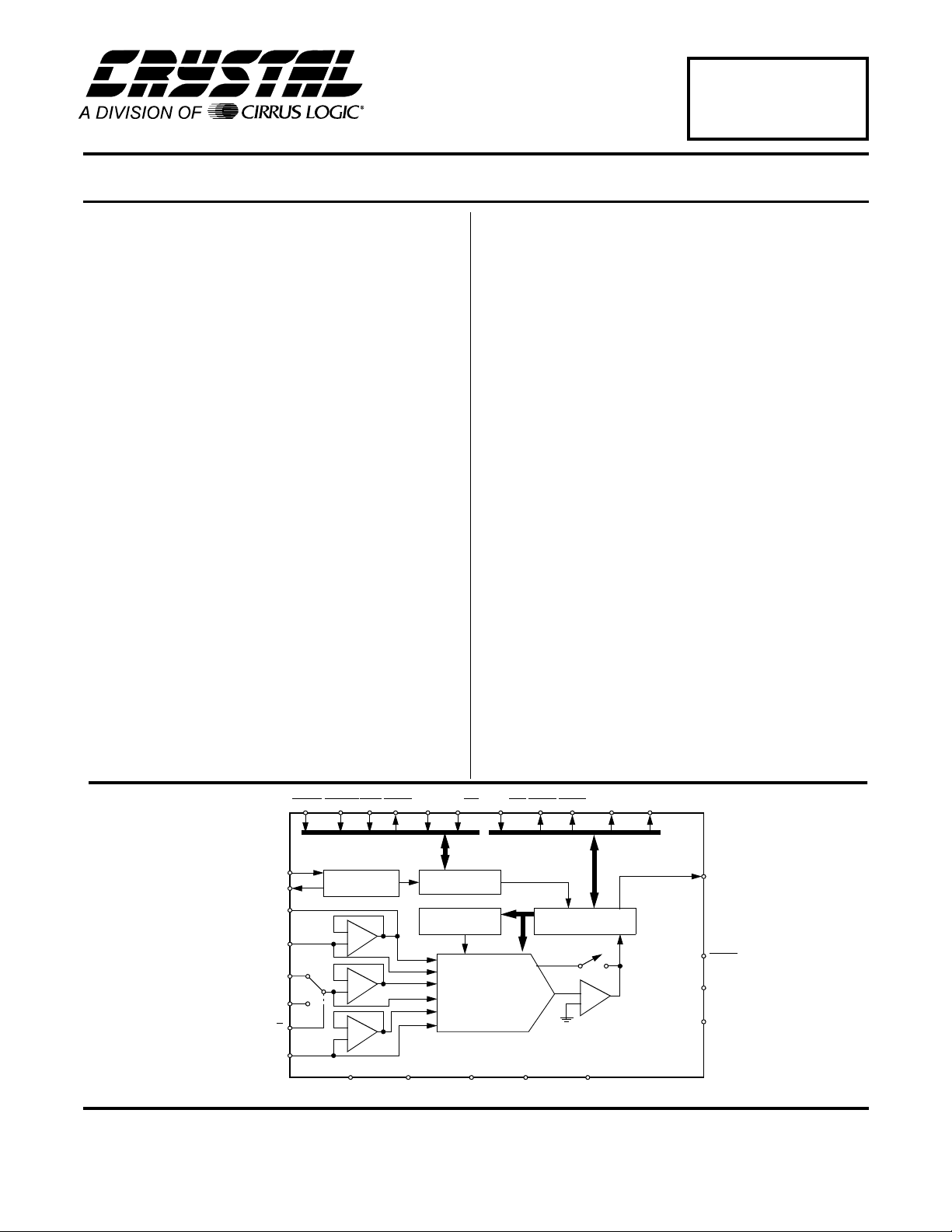
I
HOLD SLEEPRST CODEBP/UP
12 28 2 5 16 17 8 9 11 15
3
CLKIN
4
XOUT
REFBUF
VREF
AIN1
AIN2
CH1/2
AGND
Generator
21
20
19
24
13
22
Cirrus Logic, Inc.
Crystal Semiconductor Products Division
P.O. Box 17847, Austin, Texas 78760
(512) 445 7222 FAX: (512) 445 7581
http://www.crystal.com
STBY
Clock
-
+
-
+
-
+
25 23
ORDERING INFORMATION
See page 36.
TRK1
CRS/FIN
10
Control
Calibration
SRAM
16-Bit Ch arge
Redistribution
DAC
DGND VD- VD+VA-VA+
Copyright Cirrus Logic, Inc. 1997
(All Rights Reserved)
TRK2
Microcontroller
-
+
Comparator
SSH/SDL
716
SDATA
14
26
27
18
SCLK
TEST
SCKMOD
OUTMOD
MAR ‘95
DS45F2
1

CS5101A
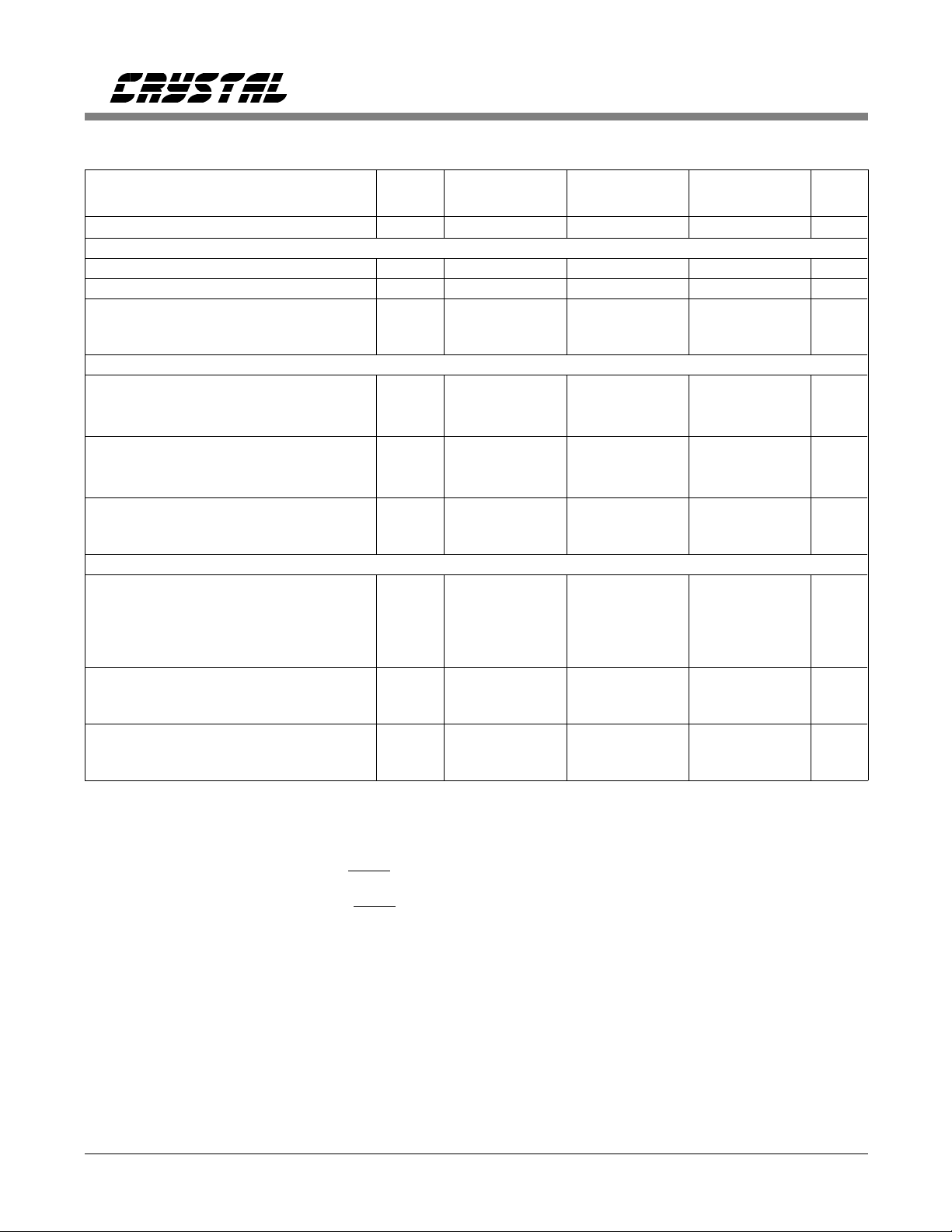
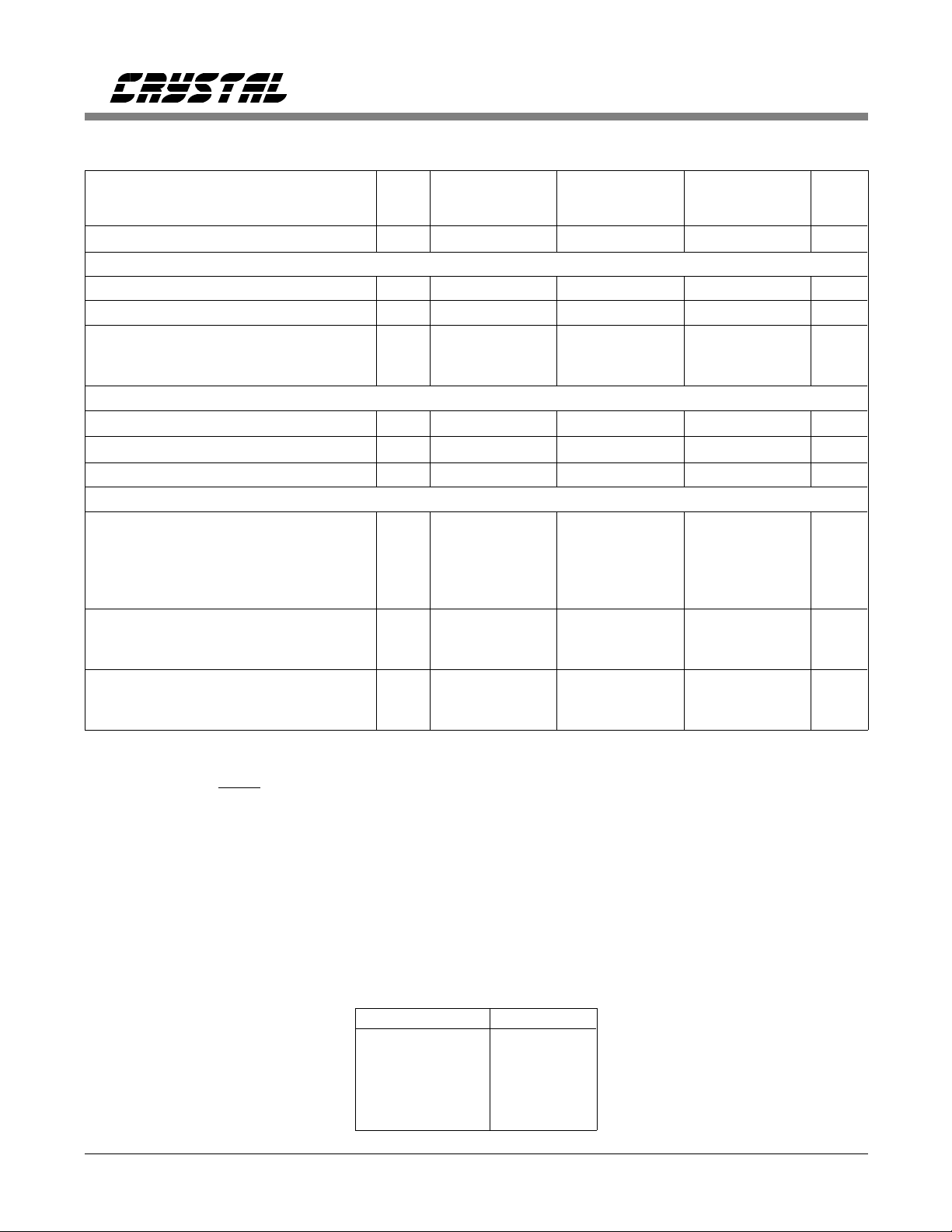
ANALOG CHARACTERISTICS (T
VREF = 4.5V; Full-Scale Input Si newave, 1 kHz; CLKIN = 4 MHz for -16, 8 MHz for -8; f
A
= T
MIN
to T
; VA+, VD+ = 5V; VA-, VD- = -5V;
MAX
= 50 kHz for -16,
s
100 kHz for -8; Bipolar Mode; FRN Mode; AIN1 and AIN2 tied together, each c hannel tested separately; A nalog
Source Impedance = 50 Ω with 1000 pF to AGND unless otherwise specified)
CS5101A-J,KCS5101A-A,B
Parameter*MinTypMaxMinTypMax Units
Specified Temperature Range0 to +70-40 to +85
°
C
Accuracy
Linearity Error -J,A,S (Note 1)
-K,B,T
Drift (Note 2)
-
0.002
-
0.001
-
±
1/4
0.003
0.002
-
-
0.002
-
0.001
-
±
1/4
0.003
0.002
-
%FS
%FS
∆
LSB
Differential Linearity(Notes 3, 4)16--16-- Bits
Full Scale Error -J,A, S ( No te 1 )
-K,B,T
Drift (Note 2)
Unipolar Offset -J,A,S (Note 1)
-K,B,T
Drift (Note 2)
Bipolar Offset -J,A,S (Note 1)
-K,B,T
Drift (Note 2)
-
±
-
±
-
±
-
±
-
±
-
±
-
±
-
±
-
±
1
1
1
1
1
±
4
±
3
-
±
2
5
±
2
4
-
±
2
5
±
2
3
-
-
±
-
±
-
±
-
±
-
±
-
±
-
±
-
±
-
±
1
±
1
4
±
1
3
-
1
±
2
5
±
2
4
-
±
2
5
±
2
3
-
2
LSB
LSB
∆
LSB
LSB
LSB
∆
LSB
LSB
LSB
∆
LSB
Bipolar Negative Ful l- S ca l e E rr o r
-J,A,S (Note 1)
-K,B,T
Drift (Note 2)
Dynamic Performance
(Bipolar Mode)
-
±
-
±
-
±
1
1
1
±
4
±
3
-
-
±
-
±
-
±
1
1
1
±
4
±
3
-
LSB
LSB
∆
LSB
Peak Harmonic or Spurious Noise (Note 1)
1 kHz Input -J,A,S
-K,B,T
12 kHz Input -J,A,S
-K,B,T
Total Harmoni c Dist ort ion -J,A, S
-K,B,T
100
98
102
85
85
88
91
--0.002
0.001--
-
96
100
-
98
102
-
85
-
85
88
91
--0.002
0.001--
-
-
-
-
dB
dB
dB
dB
%
%
96
Signal-to-Noise Ratio (Note 1)
0dB Input -J,A,S
-K,B,T
-60 dB Input -J,A,S
-K,B,T
87
90
90
92
-
30
-
32
-
87
-
90
-
-
90
92
-
30
-
32
-
-
-
-
dB
dB
dB
dB
Noise (Note 5)
Unipolar Mode
Bipolar Mode
-
35
-
70
-
-
-
35
-
70
-
-
µV
µV
rms
rms
Notes: 1. Applies after calibration at any temperature within the specified temperature range. At temp
2. Total drift over specified temperature range after calibration at power-up at 25 °C.
3. Minimum resolution for which no mis sing codes is guaranteed ov er the specified temperature range.
4. Clock speeds of less than 1.0 MHz, at temperatures >100°C will degrade DNL performance.
5. Wideband noise aliased into the baseband. Referred to the input.
*Refer to
Parameter Definitions
(immediately following the pin descriptions at the end of this data sheet).
Specifications are subject to change without notice.
2 DS45F2
CS5101A
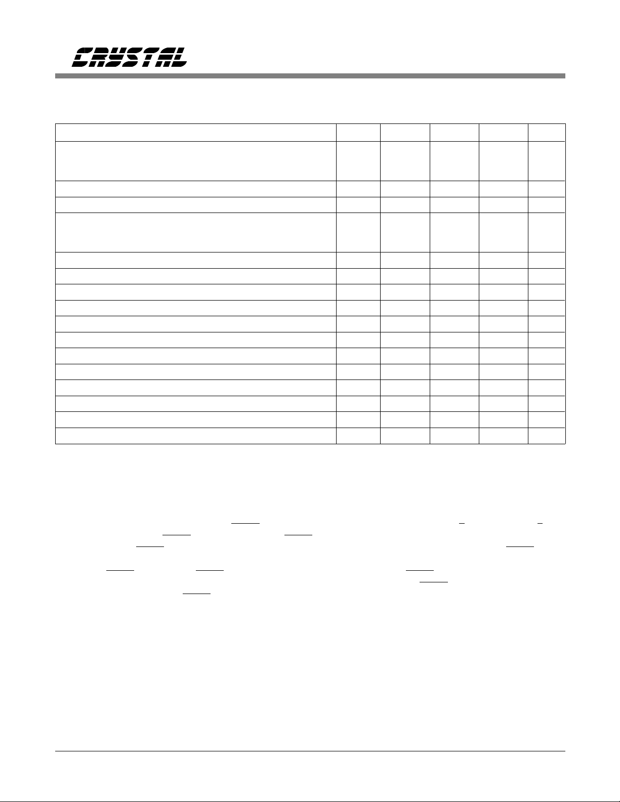
ANALOG CHARACTERISTICS (continued)
CS5101A -J,KCS5101A -A,B
Parameter*SymbolMinTypMaxMinTypMax Units
Specified Temperature Range-0 to +7040 to +85
Analog In put
Aperture Time--25--25- ns
Aperture Jitter--100--100- ps
Input Capacitance (Note 6)
Unipolar Mode
Bipolar Mode
-
-
--320
200
425
265--
320
200
425
265
Conversi on & Th roughput
Conversion Time (Note 7)
-8
-16
-
--8.12
16.25--
t
c
tc
--8.12
16.25
-
Acquisition Time (Note 8)
-8
-16
t
a
ta
-
--2.6
1.88
3.75---2.6
1.88
3.75
Throughput (Note 9)
-8
-16
tp
tp
10050-
f
f
-
--10050-
-
Power Supplies
Power Supply Current (Note 10)
Positive Analog
Negative Analog
(SLEEP High) Positi ve Digital
Negative Digital
+
I
A
-
I
A
+
I
D
-
I
D
-
21
28
-
-21
-28
-
11
15
-
-11
-15
-
21
28
-
-21
-28
-
11
15
-
-11
-15
Power Consumption (Notes 10, 11)
(SLEEP High)
(SLEEP Low)
P
do
P
ds
--3201430---3201430
Power Supply Rejection: (Note 12)
Positive Supplies
Negative Supplies
PSR
PSR
--8484-
--8484-
-
°
-
-
-
-
pF
pF
µ
µ
µ
µ
kHz
kHz
mA
mA
mA
mA
mW
mW
dB
dB
C
s
s
s
s
Notes : 6. Applies only in the track mode. When converting or calibrating, input capacitance will not exceed 30 pF.
7. Conversion time scales directly to the master clock speed. The times shown are for synchronous,
internal loop back ( FRN mode ) with 8 .0 MHz CLKIN . In PD T, RBT, and SSC m odes, as ynchro nous d elay
between the falling edge of
HOLD and the start of conversion may add to the apparent conversion time.
This delay will not exceed 1.5 master clock cycles + 10 ns. In PDT, RBT, and SSC modes, CLKIN can
be increased as long as the
HOLD sample rate is 100 kHz max.
8. The CS5101A requires 6 clock cycles of coarse charge, followed by a minimum of 1.125 µs of fine charge.
FRN mode allows 9 clock cycles for fine charge which provides for the minimum 1.125 µs with an 8 MHz
clock, however; in PDT, RBT, or SSC modes, at clock frequencies of 8 MHz or less, fine charge may
be less than 9 clock cycles. This reflects the typ. specification (6 clock cycles + 1.125 µs).
9. Throughput is the sum of the acquisition and conversion times. It will vary in accordance with conditions
affecting acquisition and conversion times, as described above.
10. All outputs unloaded. All inputs at VD+ or DGND.
11. Power co nsump tion i n the sl eep mo de appl ies with no m aster cloc k appli ed (C LKIN h eld hi gh or l ow).
12. With 300 mV p-p, 1 kHz ripple applied to each supply separately in the bipolar mode. Rejection
improves by 6 dB in the uni polar mode to 90 dB. Figure 2 3 show s a pl ot of ty pical power supp ly
rejection ve rsus f reque ncy.
DS45F2 3
CS5101A
SWITCHING CHARACTERISTICS (T
VA-, VD- = -5V ± 10%; Inputs: Logic 0 = 0V, Logi c 1 = VD+; C
= T
A
MIN
to T
L
; VA+, VD+ = 5V ± 10%;
MAX
= 50 pF)
Parameter Symbol Min Typ Max Units
CLKIN Period (Note 4)
-8
-16
CLKIN Low Time t
CLKIN High Time t
t
clk
t
clk
clkl
clkh
108
250
-
-
10,000
10,000
ns
ns
37.5 - - ns
37.5 - - ns
Crystal Frequency (Note 13)
-8
-16
f
xtal
f
xtal
2.0
2.0
-
-
9.216
4.0
MHz
MHz
SLEEP Rising to Oscillator Stable (Note 14) - - 2 - ms
RST Pulse Width t
RST to STBY Falling t
RST Rising to STBY Rising t
CH1/2 Edge to TRK1, TRK2 Rising (Note 15) t
CH1/2 Edge to TRK1, TRK2 Falling (Note 15) t
HOLD to SSH Falling (Note 16) t
HOLD to TRK1, TRK2, Falling (Note 16) t
HOLD to TRK1, TRK2, SSH Rising (Note 16) t
HOLD Pulse Width (Note 17) t
HOLD to CH1/2 Edge (Note 16) t
HOLD Falling to CLKIN Falling (Note 17) t
rst
drrs
cal
drsh1
dfsh4
dfsh2
dfsh1
drsh
hold
dhlri
hcf
150 - - ns
- 100 - ns
- 11,528,160 - t
-80-ns
- - 68t
+260 ns
clk
-60 ns
66t
clk
- 68t
+260 ns
clk
- 120 - ns
1t
+20 - 63t
clk
15 - 64t
clk
clk
ns
ns
95 - 1tc lk+10 ns
clk
Notes: 13. External loading capacitors are required to allow the crystal to oscillate. Maximum crystal frequency
is 8.0 MHz in FRN mode (100 kHz sample rate).
14. With a 8 MHz crystal, two 10 pF loading capacitors and a 10 MΩ parallel resistor (see Figure 8).
15. These times are for FRN mode.
16. SSH only works correctly if
occurs after
17. When
HOLD rises to 64 t
HOLD goes low, the analog sample is captured immediately. To start conversion, HOLD must
HOLD falling edge is within +15 to +30 ns of CH1/ 2 edge or if CH1/2 edge
after HOLD has fallen. These times are for P DT and RBT modes.
clk
be latched by a falling edge of CLKIN. Conversion will begin on the next rising edge of CLKIN after
HOLD is latched. If HOLD is operated synchronous to CLKIN, the HOLD pulse width may be as
narrow as 150 ns for all CLKIN frequencies if CLKIN falls 95 ns after
ensures that the
HOLD pulse will meet the minimum specification for t
HOLD falls. This
.
hcf
4 DS45F2
CS5102A
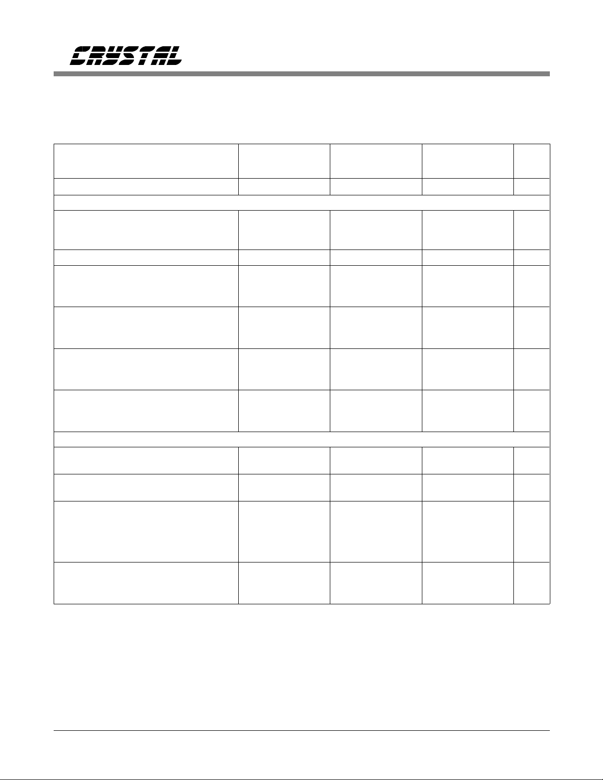
ANALOG CHARACTERISTICS (T
VREF = 4.5V; Full-Scale Input Si newave, 200 Hz; CLKIN = 1.6 MHz; f
A
= T
MIN
to T
; VA+, VD+ = 5V; VA-, VD- = -5V;
MAX
= 20 kHz; Bipolar Mode; FRN Mode;
s
AIN1 and AIN2 tied together, each channel tested separately; Anal og Source Impedance = 50 Ω with 1000pF to
AGND unless otherwise specified)
CS5102A-J,KCS5102A-A,B
Parameter*MinTypMaxMinTypMax Units
Specified Temperature Range0 to +70-40 to +85
°
C
Accuracy
Linearity Error -J,A,S (Note 1)
-K,B,T
Drift (Note 2)
-
0.002
-
0.001
-
±
1/4
0.003
0.0015
-
-
0.002
-
0.001
-
±
1/4
0.003
0.0015
-
%FS
%FS
∆
LSB
Differential Linearity(Notes 3, 18)16--16-- Bits
Full Scale Error -J,A,S (Note 1)
-K,B,T
Drift (Note 2)
Unipolar Offset -J,A,S (Note 1)
-K,B,T
Drift (Note 2)
Bipolar Offset -J,A,S (Note 1)
-K,B,T
Drift (Note 2)
Bipolar Negative -J,A,S (No te 1 )
Full-Scale Error -K,B,T
Drift (Note 2)
Dynamic Performance
(Bipolar Mode)
Peak Harmonic or -J,A,S (Note 1)
Spurious Noise -K,B,T
Total Harmoni c Dist ort ion -J,A, S
-K,B,T
-
±
2
-
±
-
-
-
-
-
-
-
-
-
-
2
±
1
±
±
±
1
±
±
±
1
±
2
±
2
±
1
9698100
102
--0.002
0.001--
±
4
±
3
-
±
1
4
±
1
3
-
±
1
4
±
1
3
-
±
4
±
3
-
-
-
-
±
-
±
-
±
-
±
-
±
-
±
1
-
±
-
±
-
±
-
±
2
-
±
-
2
±
2
9698100
102
±
2
4
±
2
3
-
1
±
1
4
±
1
3
-
±
1
4
±
1
3
-
2
±
4
±
3
-
-
-
--0.002
0.001--
LSB
LSB
∆
LSB
LSB
LSB
∆
LSB
LSB
LSB
∆
LSB
LSB
LSB
∆
LSB
dB
dB
%
%
Signal-to-Noise Ratio (Note 1)
0dB Input -J,A,S
-K,B,T
-60 dB Input -J,A,S
-K,B,T
87
90
90
92
-
30
-
32
-
87
-
90
-
-
90
92
-
30
-
32
-
-
-
-
dB
dB
dB
dB
Noise (Note 5)
Unipolar Mode
Bipolar Mode
-
35
-
70
-
-
-
35
-
70
-
-
µV
µV
rms
rms
Note: 18. Clock speeds of less than 1.6 MHz, at temperatures >100°C will degrade DNL performance.
*Refer to
Parameter Definitions
(immediately following the pin descriptions at the end of this data sheet).
Specifications are subject to change without notice.
DS45F2 5
ANALOG CHARACTERISTICS (continued)
CS5102A -J,KCS5102A -A,B
Parameter*SymbolMinTypMaxMinTypMax Units
CS5102A
Specified Temperature Range-0 to +7040 to +85
°
C
Analog In put
Aperture Time--30--30- ns
Aperture Jitter--100--100- ps
Input Capacitance (Note 6)
Unipolar Mode
-
-
--320
200
425
265--
320
200
425
265
pF
pF
Bipolar Mode
Conversi on & Th roughput
Conversion Time(Note 19)t
Acquisition Time(Note 20)t
Throughput(Note 21)f
a
tp
--40.625--40.625
c
--9.375--9.375
µ
µ
20--20-- kHz
Power Supplies
Power Supply Current (Note 22)
+
Positive Analog
Negative Analog
(SLEEP High) Positi ve Digital
Negative Digital
I
A
I
A
I
D
I
D
-
2.4
3.5
-
-
-2.4
-3.5
+
-
2.5
3.5
-
-
-1.5
-2.5
-
2.4
3.5
-
-2.4
-3.5
-
2.5
3.5
-
-1.5
-2.5
mA
mA
mA
mA
Power Consumption (Notes 11, 22)
(SLEEP High)
(SLEEP Low)
P
do
P
ds
--44165
-
--44165
mW
-
mW
Power Supply Rejection: (Note 23)
Positive Supplies
Negative Supplies
PSR
PSR--8484
-
--84
-
84
-
-
dB
dB
s
s
Notes : 19. Conversion time scales directly to the master clock speed. The times shown are for synchronous,
internal loopback (FRN mode). In PDT, RBT, and SSC modes, asynchronous delay between the falling
edge of
HOLD and the start of conversion may add to the apparent conversion time. This delay will
not exceed 1 master clock cycle + 140 ns.
20. The CS5102A requires 6 clock cycles of coarse charge, followed by a minimum of 5.625 µs of fine charge.
FRN mode allows 9 clock cycles for fine charge which provides for the minimum 5.625 µs with an 1. 6 MHz
clock, however; in PDT, RBT, or SSC modes, at clock frequencies less than 1.6 MHz, fine charge may
be less than 9 clock cycles.
21. Throughput is the sum of the acquisition and conversion times. It will vary in accordance with conditions
affecting acquisition and conversion times, as described above.
22. All outputs unloaded. All inputs at VD+ or DGND. See table below for power dissipation vs. clock frequency.
23. With 300 mV p-p, 1 kHz ripple applied to each supply separately in the bipolar mode. Rejection
improves by 6 dB in the uni polar mode to 90 dB. Figure 2 3 show s a pl ot of ty pical power supp ly
rejection ve rsus f reque ncy.
Typ. Power (mW) CLKIN (MHz)
34 0.8
37 1.0
39 1.2
41 1.4
44 1.6
6 DS45F2
CS5102A
SWITCHING CHARACTERISTICS (T
VA+, VD+ = 5V ± 10%; VA-, VD- = -5V ± 10%; Inputs: Logic 0 = 0V, Logic 1 = VD+; C
= T
A
MIN
to T
MAX
;
= 50 pF)
L
Parameter Symbol Min Typ Max Units
CLKIN Period (Note 18,24) t
CLKIN Low Time t
CLKIN High Time t
Crystal Frequency (Note 24, 25) f
clk
clkl
clkh
xtal
0.5 - 10
µ
200 - - ns
200 - - ns
0.9 1.6 2.0 MHz
SLEEP Rising to Oscillator Stable (Note 26) - - 20 - ms
RST Pulse Width t
RST to STBY Falling t
RST Rising to STBY Rising t
CH1/2 Edge to TRK1, TRK2 Rising (Note 27) t
CH1/2 Edge to TRK1, TRK2 Falling (Note 27) t
HOLD to SSH Falling (Note 28) t
HOLD to TRK1, TRK2, Falling (Note 28) t
HOLD to TRK1, TRK2, SSH Rising (Note 28) t
HOLD Pulse Width (Note 29) t
HOLD to CH1/2 Edge (Note 28) t
HOLD Falling to CLKIN Falling (Note 29) t
rst
drrs
cal
drsh1
dfsh4
dfsh2
dfsh1
drsh
hold
dhlri
hcf
150 - - ns
- 100 - ns
- 2,882,040 - t
-80-ns
- - 68t
+260 ns
clk
-60 ns
66t
clk
- 68t
+260 ns
clk
- 120 - ns
1t
+20 - 63t
clk
15 - 64t
clk
clk
ns
ns
55 - 1tc lk+10 ns
s
clk
Note: 24. Minimum CLKIN period is 0.625 µs in FRN mode (20 kHz sample rate). A t temperatures >+85 °C,
and with clock frequencies <1.6 MHz, anal og performance may be degraded.
25. External loading capacitors are required to allow the crystal to oscillate. Maximum crystal frequency
is 1.6 MHz in FRN mode (20 kHz sample rate).
26. With a 2.0 MHz crystal, two 33 pF loading capacitors and a 10 MΩ parallel resistor (see Figure 8).
27. These times are for FRN mode.
28. SSH only works correctly if
occurs after
29. When
HOLD rises to 64 t
HOLD goes low, the analog sample is captured immediately. To start conversion, HOLD must
HOLD falling edge is within +15 to +30 ns of CH1/ 2 edge or if CH1/2 edge
after HOLD has fallen. These times are for P DT and RBT modes.
clk
be latched by a falling edge of CLKIN. Conversion will begin on the next rising edge of CLKIN
HOLD is latched. If HOLD is operated synchronous to CLKIN, the HOLD pulse width may be as
after
narrow as 150 ns for all CLKIN frequencies if CLKIN falls 55 ns after
ensures that the
HOLD pulse will meet the minimum specification for t
HOLD falls. This
.
hcf
DS45F2 7
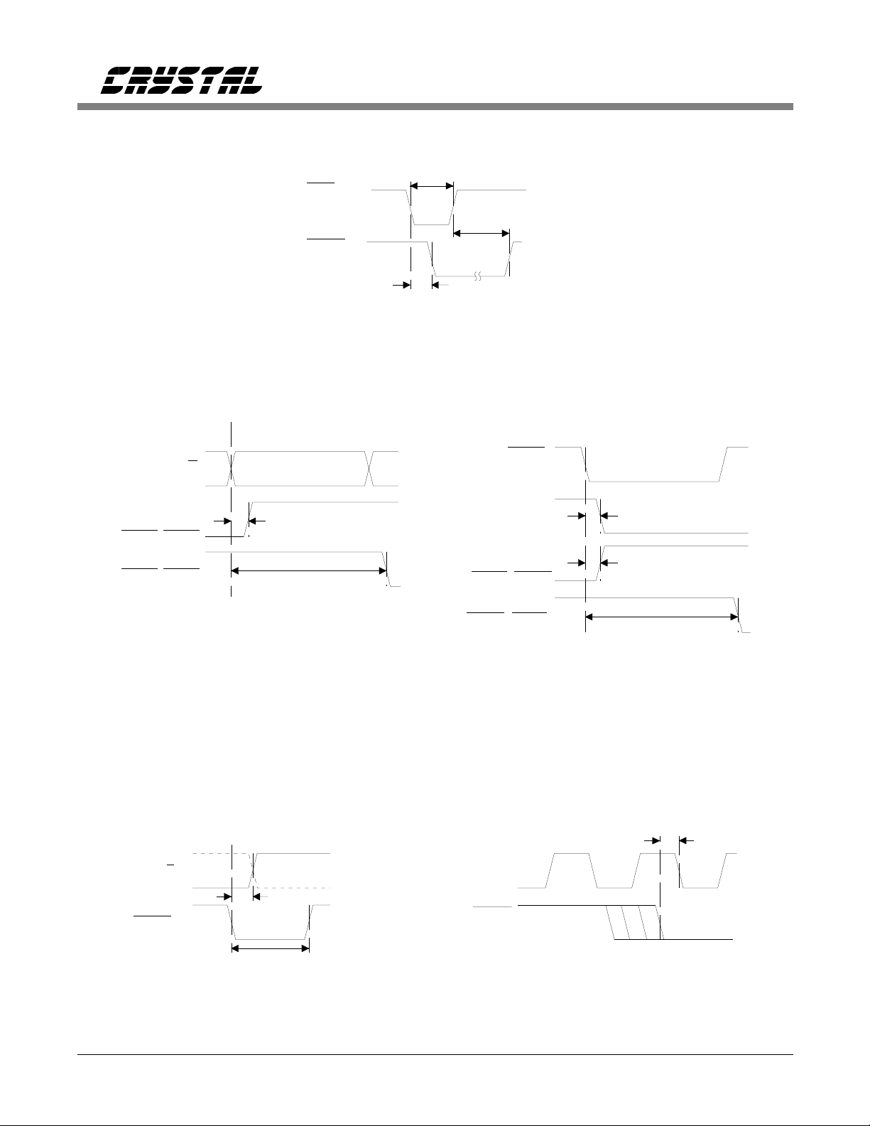
t
rst
RST
STBY
t
drrs
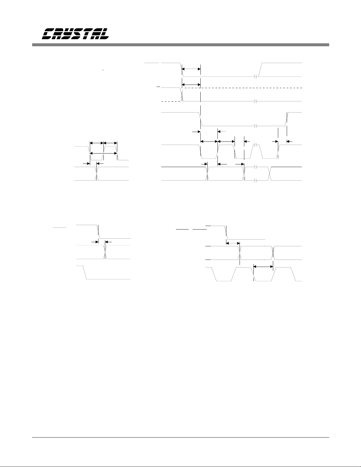
Reset and Calibration Timing
CS5101A CS5102A
t
cal
CH1/2
TRK1,TRK2
TRK1,TRK2
HOLD
SSH/SDL
t
drsh1
t
dfsh4
SSH,TRK1,TRK2
TRK1,TRK2
t
dfsh2
t
drsh
t
dfsh1
a. FRN Mode b. PDT, RBT Mode
Control Output Timing
t
hcf
CH1/2
CLKIN
HOLD
Start Conversion Timing
HOLD
t
dhlri
t
hold
Channel Selection Timing
8 DS45F2
SWITCHING CHARACTERISTICS (Continued)
Parameter Symbol Min Typ Max Units
PDT and RBT Modes
SCLK Input Pulse Period t
SCLK Input Pulse Width Low t
SCLK Input Pulse Width High t
SCLK Input Falling to SDATA Vali d t
HOLD Falling to SDATA Valid PDT Mode t
TRK1, TRK2 Falling to SDATA Valid (Note 30) t
FRN and SSC Modes
SCLK Output Pulse Width Low t
SCLK Output Pulse Width High t
SDATA Valid Before Rising SCLK t
SDATA Valid After Rising SCLK t
SDL Falling to 1st Rising SCLK t
Last Rising SCLK to SDL Rising CS5101A
CS5102A
HOLD Falling to 1st Falling SCLK CS5101A
CS5102A
CH1/2 Edge to 1st Falling SCLK t
sclk
sclkl
sclkh
dss
dhs
dts
slkl
slkh
ss
sh
rsclk
t
rsdl
t
rsdl
t
hfs
thfs
chfs
CS5101A CS5102A
200 - - ns
50 - - ns
50 - - ns
- 100 150 ns
- 140 230 ns
- 65 125 ns
-2t
-2t
2t
-100 - - ns
clk
2t
-100 - - ns
clk
-2t
-
-
6tclk
6t
clk
2t
2tclk
clk
clk
clk
clk
-
-
-7tclk-t
-t
-t
-ns
2tclk+165
+200nsns
2t
clk
8t
+165
clk
+200nsns
8t
clk
clk
clk
clk
Note: 30. Only valid for TRK1, TRK2 falling when SCLK is low. If SCLK is high when TRK1, TRK2 falls, then
SDATA is valid t
DIGITAL CHARACTERISTICS (T
VD- =
5V ± 10%)
time after the next falling SCLK .
dss
= T
A
min
to T
; VA+, VD+ = 5V ± 10%; VA-,
max
Parameter Symbol Min Typ Max Units
Calibration Memory Retention (Note 31)
V
MR
2.0 - - V
Power Supply Voltage VA+ and VD+
High-Level Input Voltage V
Low-Level Input Voltage V
High-Level Output Voltage (Note 32) V
Low-Level Output Voltage I
= 1.6 mA V
OUT
Input Leakage Current I
Digital Output Pin Capacitance C
IH
IL
OH
OL
in
out
2.0 - - V
--0.8V
(VD+)-1.0 - - V
--0.4V
--10
µA
-9-pF
Notes: 31. VA- and VD- can be any value from zero to -5V for memory retention. Neither VA- or VD- should be
allowed to go positive. AIN1, AIN2 or VREF must not be greater than VA+ or VD+.
This parameter is guaranteed by characterization.
32. I
= -100 µA. This specification guarantees TTL compatibility (VOH = 2.4V @ Iout = -40 µA).
OUT
DS45F2 9
CS5101A CS5102A
t
HOLD
CH1/2
SSH/SDL
t
sclkltsclkh
SCLK
t
SCLK
SDATA
t
dss
sclk
SDATA
a. SCLK input (RBT and PDT mode) b. SCLK output (SSC and FRN modes)
Serial Data Timing
hfs
t
chfs
t
rsclk
slkl
t
slkh
t
dss
t
sh
t
t
ss
MSB
LSB
t
rsdl
HOLD
SDATA
SCLK
t
dhs
MSB
TRK1, TRK2
SDATA
SCLK
t
dts
MSB
t
dss
a. Pipelined Data Transmission (PDT) b. Register Burst Transmission (RBT) Mode
Data Transmission Timing
MSB-1
10 DS45F2

CS5101A CS5102A
RECOMMENDED OPERATING CONDITIONS (AGND, DGND = 0V, see Note 33)
Parameter Symbol Min Typ Max Units
DC Power Supplies: Positive Digital
Negative Digital
Positive Analog
Negative Analog
VD+
VD-
VA+
VA-
4.5
-4.5
4.5
-4.5
5.0
-5.0
5.0
-5.0
VA+
-5.5
5.5
-5.5
V
V
V
V
Analog Reference Voltage VREF 2.5 4.5 (VA+)-0.5 V
Analog Input Voltage: (Note 34)
Unipolar
Bipolar
V
AIN
V
AIN
AGND
-VREF
-
-
VREF
VREF
V
V
Notes: 33. All voltages with respect to ground.
34. The CS5101A and CS5102A can accept input voltages up to the analog supplies (VA+ and VA-). They
will produce an output of all 1’s for inputs above VREF and all 0’s for inputs below AGND in unipolar
mode and -VREF in bipolar mode, with binar y coding (CODE = low).
ABSOLUTE MAXIMUM RATINGS* (AGND, DGND = 0V, all voltages with respect to ground)
Parameter Symbol Min Typ Max Units
DC Power Supplies: Positive Digital (Note 35)
Negative Digital
Positive Analog
Negative Analog
Input Current, Any Pin Except Supplies (Note 36) I
Analog Input Voltage (AIN and VREF pins) V
Digital Input Voltage V
Ambient Operating Temperature T
Storage Temperature T
Ambient Operating Temperature T
Storage Temperature T
VD+
VD-
VA+
VA-
in
INA
IND
A
stg
A
stg
-0.3
0.3
-0.3
0.3
--
-
-
-
-
6.0
-6.0
6.0
-6.0
±
10
mA
(VA-)-0.3 - (VA+)+ 0.3 V
-0.3 - (VA+)+0.3 V
-55 - 125
-65 - 150
-55 - 125
-65 - 150
°
°
°
°
V
V
V
V
C
C
C
C
Notes: 35. In addition, VD+ must not be greater than ( VA+) +0.3V
36. Transient currents of up to 100 mA will not cause SCR latch-up.
*WARNING: Operation beyond these limits may result in permanent damage to the devi ce.
DS45F2 11
CS5101A CS5102A
GENERAL DESCRIPTION
The CS5101A and CS5102A are 2-channel, 16bit A/D converters. The devices include an
inherent sample/hold and an on-chip analog
switch for 2-channel operation. Both channels
can thus be sampled and converted at rates up to
50 kHz each (CS5101A) or 10 kHz each
(CS5102A). Alternatively, each of the devices
can be operate d as a single channel ADC operating at 100 kHz (CS5101A) or 20 kHz
(CS5102A).
Both the CS5101A and CS5102A can be configured to accept either unipolar or bipolar input
ranges, and data is output serially in either binary
or 2’s complement coding. The devices can be
configured in 3 different output modes, as w ell as
an internal, synchronous loopback mode. The
CS5101A and CS5102A provide coarse
charge/fine charge control, to allow accurate
tracking of high-slew sign als.
THEORY OF OPERATION
The CS5101A and CS5102A implement the successive approximation algorithm using a charge
redistribution architecture. Instead of the traditional resistor network, the DAC is an array of
binary-weighted capacitors. All capacitors in the
array share a common node at the comparator’s
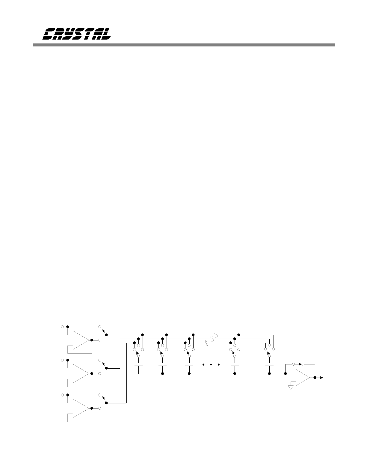
input. As shown in Figure 1, their other terminals
are capable of being connected to AGND, VRE F,
or AIN (1 or 2). When the device is not calibrating or converting, all capacitors are tied to AIN.
Switch S1 is closed and the charge on the array,
tracks the input signal.
When the conversion command is issued, switch
S1 opens. This traps the charge on the comparator side of the capacitor array and creates a
floating node at the comparator ’s input. The co nversion algorithm operates on this fixed charge,
and the signal at the analog input pin is ignored.
In effect, the entire DAC capacitor array serves
as analog memory during conversion much like a
hold capacitor in a sample/hold amplifier.
The conversion consists of manipulating the free
plates of th e capacitor array to VREF and AGND
to form a capacitive divider. Since the charge at
the floating node remains fixed, the voltage at
that point depends on the proportion of capacitance tied to VREF versus AGND. The
successive-approximation algorithm is used to
find the proportion of capacitance, which when
connected to the reference will drive the voltage
at the floating node to zero. That binary fraction
of capacitance represents the converter’s digital
output.
AIN
Fine
+
-
VREF
+
-
AGND
+
-
12 DS45F2
Coarse
Fine
Coarse
Fine
Coarse
Figure 1. Coarse Charge Input Buffers and Charge Redistribution DAC
C
Bit 15 Bit 14 Bit 13 Bit 0
MSB LSB
C/2 C/32,768
C = C + C/2 + C/4 + C/8 + ... C/32,768
tot
C/4
C/32,768
Dummy
S1
-
+

CS5101A CS5102A
Calibration
The ability of the CS5101A or the CS5102A to
convert accurately to 16-bits clearly depends on
the accuracy of its comparator and DAC. Each
device utilizes an "auto-zeroing" scheme to null
errors introduced by the comparator. All offsets
are stored on the capacitor array while in the
track mode and are effectively subtracted from
the input signal when a conversion is initiated.
Auto-zeroing enhances power supply rejection at
frequencies well below the conversion rate.
To achieve 16-bit accuracy from the DAC, the
CS5101A and CS5102A use a novel self-calibration scheme. Each bit capacitor shown in
Figure 1 actually consists of several capacitors in
parallel which can be manipulated to adjust the
overall bit weight. An on-chip micro controller
precisely adjusts each capacitor with a resolution
of 18 bits.
The CS5101A and CS5102A should be reset
upon power-up, thus initiating a calibration cycle.
The device then stores its calibration coefficients
in on-chip SRAM. When the CS5101A and
CS5102A are in power-down mode (SLEEP
low), they retain the calibration coefficients in
memory, and need not be recalibrated when normal operation is resumed.
OPERATION OVERVIEW
Monolithic design and inherent sampling architecture make the CS5101A and CS5102A
extremely easy to use.
Initiating Conversions
A falling transition on the HOLD pin places the
input in the hold mo de and initiates a conversion
cycle. The charge is trapped on the capacitor array the instant HOLD goes low. The device will
complete conversion of the sample within 66
master clock cycles, then automatically return to
the track mode. After allowing a short time for
acquisition, the device will be ready for another
conversion.
In contrast to systems with separate track-andholds and A/D converters, a sampling clock can
simply be connected to the HOLD input. The
duty cycle of this clock is not critical. The HOLD
input is latched internally by the master clock, so
it need only remain low for 1/f
+ 20 ns, but no
clk
longer than the minimum conversion time minus
two master clocks or an additional conversion cycle will be initiated with inadequate time for
acquisition. In Free Run mode, SCKMOD =
OUTMOD = 0, the device will convert at a rate
of CLKIN/80, and the HOLD inp ut is ignored.
As with any high-resolution A-to-D system, it is
recommended that sampling is synchronized to
the master system clock in order to minimize the
effects of clock feedthrough. However, the
CS5101A and CS5102A may be operated entirely
asynchronous to the master clock if necessary.
Tracking the Input
Upon completing a conversion cycle the
CS5101A and CS5102A immediately return to
the track mode. The CH1/2 pin directly controls
the input switch, and therefore directly determines which channel will be tracked. Ideally, the
CH1/2 pin should be switched during the conversion cycle, thereby nullifying the input mux
switching time, and guaranteeing a stable input at
the start of acquisition. If, however, the CH1/2
control is changed during the acquisition phase,
adequate coarse charge and fine charge time must
be allowed before initiating conversion.
When the CS5101A or the CS5102A enters tracking mode, it uses an internal input buffer
amplifier to provide the bulk of the charge on the
capacitor array (coarse-charge), thereby reducing
the current load on the external analog circuitry.
Coarse-charge is internally initiated for 6 clock
cycles at the end of every conversion. The buffer
DS45F2 13

CS5101A CS5102A
amplifier is then bypassed, and the capacitor array is directly connected to the input. This is
referred to as fine-charge, during which the
charge on the array is allowed to accurately settle
to the input voltage (see Figure 10).
With a full scale input step, the coarse-charge input buffer of the CS5101A will charge the
capacitor array within 1% in 650 ns. The converter timing allows 6 clock cycles for coarse
charge settling time. When the CS5101A
switches to fine-charge mode, its slew rate is
somewhat reduced. In fine-charge, the CS5101A
can slew at 2 V/µs in unipolar mode. In bipolar
mode, only half the capacitor array is connected
to the analog input, so the CS5101A can slew at
4V/µs.
With a full scale input step, the coarse-charge input buffer of the CS5102A will charge the
capacitor array within 1% in 3.75 µs. The converter timing allows 6 clock cycles for coarse
charge settling time. When in fine-charge mode,
the CS5102A can slew at 0.4 V/µs in unipolar
mode; and at 0.8 V/µ s in bipolar mode.
Acquisition of fast slewing signals can be hastened if the voltage change occurs during or
immediately following the conversion cycle. For
instance, in multiple channel applications (using
either the device’s internal channel selector or an
external MUX), channel selection should occur
while the CS5101A or the CS5102A is converting. Multiplexer switching and settling time is
thereby removed from the overall throughput
equation.
If the input signal changes drastically during the
acquisition period (such as changing the signal
source), the device should be in co arse-charge for
an adequate period following the change. The
CS5101A and CS5102A can be forced into
coarse-charge by bringing CRS/FIN high. The
buffer amplifier is engaged when CRS/FIN is
high, and may be switched in any number of
times during tracking. If CRS/FIN is held low,
the CS5101A and CS5102A will only coarsecharge for the first 6 clock cycles following a
conversion, and will stay in fine-charge until
HOLD goes low. To get an accurate sample using
the CS5101A, at least 750 ns of coarse-charge,
followed by 1.125 µs of fine-charge is required
before initiating a conversion. If coarse charge is
not invoked, then up to 25 µs should be allowed
after a step change input for proper acquisition.
To get an accurate sample using the CS5102A, at
least 3.75 µs of coarse-charge, followed by
5.625 µs of fine-charge is required before initiat-
ing a conversion (see Figure 2). If coarse charge
is not invoked, then up to 125 µs should be allowed after a step change input for proper
acquisition. The CRS/FIN pin must be low prior
to HOLD becoming active and be held low during conversion.
Master Clock
The CS5101A and CS5102A can operate either
from an externally-supplied master clock, or from
their own crystal oscillator (with a crystal). To
enable the internal crystal oscillator, simply tie a
crystal across the XOUT and CLKIN pins and
add 2 capacitors and a resistor, as shown on the
system connec tion di agram in Figure 8.
Calibration and conversion times directly scale to
the master clock frequency. The CS5101A-8 can
operate with clock or crystal frequencies up to
9.216 MHz (8.0 MHz in FRN mode). This allows
maximum throughput of up to 50 kHz per channel in dual-channel operation, or 100 kHz in a
single channel configuration. The CS5101A-16
can accept a maximum clock speed of 4 MHz,
with corresponding throughput of 50 kHz. The
CS5102A can operate with clock or crystal freq uencies up to 2.0 MHz (1.6 MHz in FRN mode). This
allows maximum throughput of up to 10 kHz per
channel in dual-channel operation, or 20 kHz in a
single channel configuration. For 16 bit performance
a 1.6 MHz clock is recomme nded. This 1.6 MHz
14 DS45F2

CLKIN
CRS/FIN
Internal
Status
Conv.
CS5101A CS5102A
Min: 750 ns*
3.75 µs**
Min: 1.125 µs*
6 clk
Coarse Fine Chg. Coarse Fine Chg. Conv.
5.625 µs**
TRK1 or
TRK2
HOLD
* Applies to 5101A
** Applies to 5102A
2 clk
Figure 2. Coarse-Charge/Fine-Charge Control
clock yields a maximum throughput of 20 kHz in
a single channel configuration.
Asynchronous Sampling Considerations
When HOLD goes low, the analog sample is captured immediately. The HOLD signal is latched
by the next falling edge of CLKIN, and conversion then starts on the subsequent rising edge. If
HOLD is asynchronous to CLKIN, then there
will be a 1.5 CLKIN cycle uncertainty as to when
conversion starts. Considering the CS5101A with an
8 MHz CLKIN, with a 100 kHz HOLD signal, then
this 1.5 CLKIN uncertainty will result in a 1.5
CLKIN period possible reduction in fine charge time
for the next conversion .
Unipolar Input
Voltage
>(VREF-1.5 LSB) FFFF 7FFF >(VREF- 1.5 LSB)
VREF-1.5 LSB FFFF
VREF/2-0.5 LSB 8000
+0.5 LSB 0001
<(+0.5 LSB) 0000 8000 <(-VREF+0.5 LSB)
Offset
Binary
FFFE
7FFF
0000
Table 1. Output Coding
Two’s
Complement
7FFF
7FFE
0000
FFFF
8001
8000
Bipolar Input
Voltage
VREF-1.5 LSB
-0.5 LSB
-VREF+0.5 LSB
This reduced fine charge time will be less than
the minimum specification. If the CLKIN frequency is increased slightly (for example, to
8.192 MHz) then sufficient fine charge time will
always occur. The maximum frequency for
CLKIN is specified at 9.216 MHz; it is recommended that for asynchronous operation at
100 kHz, CLKIN should be between 8.192 MHz
and 9.216 MHz.
Analog Input Range/Coding Format
The reference voltage directly defines the input
voltage range in both the unipolar and bipolar
configurations. In the unipolar configuration
(BP/UP low), the first code transition occurs 0.5
LSB above AGND, and the final code transition
occurs 1.5 LSB’s below VREF. In the bipolar
configuration (BP/UP high), the first code transition occurs 0.5 LSB above -VREF and the last
transition occurs 1.5 LSB’s below +VREF.
The CS5101A and CS5102A can output data in
either 2’s complement, or binary format. If the
CODE pin is high, the output is in 2’s complement format with a range of -32,768 to +32,767.
If the CODE pin is low, the output is in binary
format with a range of 0 to +65,535. See Table 1
for output coding.
DS45F2 15

CS5101A CS5102A
MODE
PDT
RBT
SSC
FRN
SCKMOD
1
1
0
0
OUTMOD
Table 2. Serial Output Modes
Output Mode Control
The CS5101A and CS5102A can be configured
in three different output modes, as well as an internal, synchron ous loop-back mode. This allows
great flexibility for design into a wide variety of
systems. The operating mode is selected by setting the states of the SCKMOD and OUTMOD
pins. In all modes, data is output on SDATA,
starting with the MSB. Each subsequent data bit
is updated on the falling edge of SCLK.
When SCKMOD is high, SCLK is an input, allowing the data to be clocked out with an
external serial clock at rates up to 5 MHz. Additional clock edges after #16 will clock out logic
’1’s on SDATA. Tying SCKMOD low reconfigures SCLK as an output, and the converter clocks
SCLK
1
0
1
0
Input
Input
Output
Output
CH1/2
Input
Input
Input
Output
HOLD
Input
Input
Input
X
out each bit as it’s determined during the conversion process, at a rate of 1/4 the master clock
speed. Table 2 shows an overview of the different
states of SCKMOD an d OUTMOD, and the corresponding output modes.
Pipelined Data Transmission (PDT)
PDT mode is selected by tying both SCKMOD
and OUTMOD high. In PDT mode, the SCLK
pin is an input. Data is registered during conversion, and output during the following conversion
cycle. HOLD must be brought low, initiating another conversion, before data from the previous
conversion is available on SDATA. If all the data
has not been clocked out before the next falling
edge of HOLD, the old data will be lost
(Figure 3).
68 72 760 4 8 64687276 4 8
60 6000
CLKIN (i)
HOLD (i)
CH1/2 (i)
Internal
Status
SCLK (i)
SDATA (o)
SSH/SDL (o)
TRK1 (o)
TRK2 (o)
16 DS45F2
Converting Ch. 2
D15 D14
Tracking Ch. 1 Tracking Ch. 2
D1
D0 (Ch. 1)
Figure 3. Pipelined Data Transmission Mo de (PDT)
Converting Ch. 1
D15 D14
D1
64
D0 (Ch. 2)
D15

CS5101A CS5102A
CLKIN (i)
HOLD (i)
CH1/2 (i)
Internal
Status
SCLK (i)
SDATA (o)
SSH/SDL (o)
TRK1 (o)
TRK2 (o)
CLKIN (i)
HOLD (i)
CH1/2 (i)
Internal
Status
04 40
Converting Ch. 2 Converting Ch. 1
64
68
72
Tracking Ch. 1 Tracking Ch. 2
Channel 2 Da ta Channel 1 Data
D0 D0
Figure 4. Registered Burst Transmission Mode (RBT)
64
68
72
76
Converti ng Ch. 2 Tracking Ch. 1 Converting Ch. 1
4
64
8640066
68 72
68
72 76048
Tracking Ch. 2
0
SCLK (o)
SDATA (o)
SSH/SDL (o)
TRK1 (o)
TRK2 (o)
CLKIN (i)
CH1/2 (o)
Internal
Status
SCLK (o)
SDATA (o)
SSH/SDL (o)
TRK1 (o)
TRK2 (o)
D15 D14 D1 D0 (Ch. 2)
D15 D14 D1 D0 (Ch. 1)
Figure 5. Synchronous Self-Clocking Mode (SSC)
68
64
68
72
7 69 7
Converting Ch. 2 Tracking Ch. 1 Converting Ch. 1 Tracking Ch. 2
D15 D1 D0 (Ch. 2)
76 4 8 640
D15 D1 D0 (Ch. 1)
69
72 76048
0
Figure 6. Free Run Mode (FRN)
DS45F2 17

CS5101A CS5102A
Registered Burst Transmission (RBT)
RBT mode is selected by tying SCKMOD high,
and OUTMOD low. As in PDT mode, SCLK is
an input, however data is available immediately
following conversion, and may be clocked out
the moment TRK1 or TRK2 falls. The falling
edge of HOLD clears the output buffer, so any
unread data will be lost. A new conversion may
be initiated before all the data has been clocked
out if the unread data bits are not important
(Figure 4).
Synchronous Self-Clocking (SSC)
SSC mode is selected by tying SCKMOD low,
and OUTMOD high. In SSC mode, SCLK is an
output, and will clock out each bit of the data as
it’s being converted. SCLK will remain high between conversions, and run at a rate of 1/4 the
master clock speed for 16 low pulses during conversion (Figure 5).
The SSH/SDL goes low coincident with the first
falling edge of SCLK, and returns high 2 CLKIN
cycles after the last rising edge of SCLK. This
signal frames the 16 data bits and is useful for
interfacing to shift registers (e.g. 74HC595) or to
DSP serial ports.
Free Run (FRN)
Free Run is the internal, synchronous loopback
mode. FRN mode is selected by tying SCKMOD
and OUTMOD low. SCLK is an output, and operates exactly the same as in the SSC mode. In
Free Run mode, the converter initiates a new
conversion every 80 master clock cycles, and alternates between channel 1 and channel 2. HOLD
is disabled, and should be tied to either VD+ or
DGND. CH1/2 is an output, and will change at
the start of each new con version cycle, in dicating
which channel will be tracked after the current
conversion is finished (Figure 6).
The SSH/SDL goes low coincident with the first
falling edge of SCLK, and returns high 2 CLKIN
cycles after the last rising edge of SCLK. This
signal frames the 16 data bits and is useful for
interfacing to shift registers (e.g. 74HC595) or to
DSP serial ports.
SYSTEM DESIGN WITH THE CS5101A AND CS5102A
Figure 7 shows a general system connection diagram for the CS51 01A and CS5102A.
Digital Circuit C onnections
When TTL loads are utilized the potential for
crosstalk between digital and analog sections of
the system is increased. This crosstalk is due to
high digital supply and signal currents arising
from the TT L drive current required of each digital output. Connecting CMOS logic to the dig ital
outputs is recommended. Suitable logic families
include 4000B, 74HC, 74AC, 74ACT, and
74HCT.
System Initialization
Upon power up, the CS5101A and CS5102A
must be reset to guarantee a consistent starting
condition and initially calibrate the device. Due
to each device’s low power dissipation and low
temperature drift, no warm-up time is required
before reset to accommodate any self-heating effects. However, the voltage reference input
should have stabilized to within 0.25% of its final
value before RST rises to guarantee an accurate
calibration. Later, the CS5101A and CS5102A
may be reset at any time to initiate a single full
calibration.
When RST is brought low all internal logic
clears. When RST returns high on the CS5101A,
a calibration cycle begins which takes 11,528,160
master clock cycles to complete (approximately
1.4 seconds with an 8 MHz master clock). The
18 DS45F2

CS5101A CS5102A
+5VA
VD+
Mode Control
Voltage Reference
Analog
Sources
* For best dynamic
S/(N+D) performance.
-5VA
50
1 nF
50
1 nF
+
*
*
4.7
0.1 µF
µ
NPO
NPO
F 0.1 µF
18
OUTMOD
27
SCKMOD
17
BP/UP
16
CODE
20
VREF
22
AGND
19
AIN1
24
AIN2
21
REFBUF
10
25 7
26
VA+ VD+
CS5101A
CS5102A
VA- VD -
23 1
TST
OR
CRS/FIN
SSH/SDL
10
XOUT
CLKIN
RST
SLEEP
STBY
CH1/2
HOLD
TRK1
TRK2
SCLK
SDATA
DGND
4
XTAL
3
2
28
5
13
10
12
8
9
11
14
15
6
+
1 µF0.1 µF
C1
10 M
C2 = C1
Control
Logic
PDT, RBT,
SSC
PDT, RB T,
SSC
Data
Interface
Unused Logic inputs should
be tied to VD+ or DGND.
EXT
CLOCK
XTAL & C1 Table
CS5101A
FRN
CS5102A
FRN
XTAL
8.0 MHz
8.192 MHz
1.6 MHz
1.6 MHz
or
2.0 MHz
C1, C2
10 pF
10 pF
30 pF
30 pF
4.7
µ
F 0.1 µF1
++
µ
F0.1 µF
Figure 7. CS5101A/CS5102A System Connection Diagram
calibration cycle on the CS5102A takes
2,882,040 master clock cycles to complete (approximately 1.8 seconds with a 1.6 MHz master
be less than or equal to 10 kΩ. The system power
supplies, voltage reference, and clock should all
be established prior RST rising.
clock). The CS5101A’s and CS5102A’s STBY
output remains low through out the calibration se-
Single-Channel Operation
quence, and a rising transition indicates the
device is ready for normal operation. While calibrating, the CS5101A and CS5102A will ignore
changes on the HOLD input.
The CS5101A and CS5102A can alternatively be
used to sample one channel by tying the CH1/2
input high or low. The unused AIN pin should be
tied to the analog input signal or to AGND. (If
To perform the reset function, a simple power-on
operating in free run mode, AIN1 and AIN2 must
reset circuit can be built using a resistor and capacitor as shown in Figure 8. The resistor should
DS45F2 19

CS5101A
1N4148
+5V
R
C
Figure 8. Power-up Reset Circuit
VD+
____
RST
OR
CS5102A
be tied to the same source, as CH1/2 is reconfigured as an output.)
ANALOG CIRCUIT CONNECTIONS
Most popular successive approximation A/D converters generate dynamic loads at their analog
connections. The CS5101A and CS5102A internally buffer all analog inputs (AIN1, AIN2,
VREF, and AGND) to ease the demands placed
on external circuitry. However, accurate system
operation still requires careful attention to details
at the design stage regarding source impedances
as well as grounding and decoupling schemes.
Reference Considerations
An application note titled "Voltage References for
the CS501X Series of A/D Converters" is avail-
ab le for the CS5101A and CS5102A. In addition to
working through a reference circuit design example,
it offers several built-and-tested reference circuits.
CS5101A CS5102A
tegrity. Whenever the array is switched during
conversion, the buffer is used to coarse-charge
the array thereby providing the bu lk of the necessary charge. The appropriate array capacitors are
then switched to the unbu ffered VREF pin to avoid
any errors due to offsets and/or noise in the buffer.
The external reference circuitry need only provide the residual charge required to fully charge
the array after coarse-charging from the buffer.
This creates an ac current load as the CS5101A
and CS5102A sequence through conversions. The
reference circuitry must have a low enough output impedance to drive the requisite current
without changing its output voltage significantly.
As the analog input signal varies, the switching
sequence of the internal capacitor array changes.
The current load on the external reference circuitry thus varies in response with the analog
input. Therefore, the external reference must not
exhibit significant peaking in its output impedance characteristic at signal frequencies or their
harmonics.
A large capacitor connected between VREF and
AGND can provide sufficiently low output impedance at the high end of the frequency
spectrum, while almost all precision references
exhibit extremely low output impedance at dc.
The presence of large capacitors on the output of
some voltage references, however, may cause
peaking in the output impedance at intermediate
frequencies. Care should be exercised to ensure
that significant peaking does not exist or that
some form of compensation is provided to eliminate the effect.
During conversion, each capacitor of the calibrated capacitor array is switched between VREF
and AGND in a manner determined by the successive-approximation algorithm. The charging
and discharging of the array results in a current
load at the reference. The CS5101A and
CS5102A each include an internal buffer ampli-
fier to minimize the external reference circuit’s
The magnitude of the current load o n the external
reference circuitry will scale to the master clock
frequency. At the full-rated 9.216 MHz clock
(CS5101A), the reference must supply a maximum load current of 20 µA peak-to-peak (2 µA
typical). An output impedance of 2 Ω will there-
fore yield a maximum error of 40 µV. At t h e
full-rated 2.0 MHz clock (CS5102A), the refer-
drive requirement and preserve the reference’s in-
20 DS45F2

V
ref
10 µF
+V
CS5101A CS5102A
+200
ee
20
VREF
21
0.01 µF
0.1
REFBUF
µ
F
+100
-100
0
Fine-ChargeCoarse-Charge
R*
R=
-5V
2π (C
23
1
+ C2) f
1
VA-
CS5101A
OR
CS5102A
peak
Figure 9. Reference Connections
ence must supply a maximum load current of
5 µA peak-to-peak (0.5 µA typical). An output
impedance of 2 Ω will therefore yield a maxi-
mum error of 10.0 µV. With a 4.5 V reference and
LSB size of 138 µV this would insure approxi-
mately 1/14 LSB accuracy. A 10 µF capacitor
exhibits an impedance of less than 2 Ω at fre-
quencies greater than 16 kHz. A high-quality
tantalum capacitor in parallel with a smaller ceramic capacitor is recommended.
-200
-300
Internal Charge Error (LSB’s)
-400
8 MHz Clock
2.0 MHz Clock
0.25
1.0
0.5 0.75 1.0
2.0 3.0 4.0
Acquisition Time (us)
Figure 10. Charge Settling Time
(8 and 2.0 MHz Clocks)
reference voltage approaches VA+ thereby increasing external drive requirements at VREF. A
4.5V reference is the maximum reference voltage
recommended. This allows 0.5V headroom for
the internal reference buffer. Also, the buffer enlists the aid of an external 0.1 µF ceramic
capacitor which must be tied between its output,
REFBUF, and the negative analog supply, VA-.
For more information on references, consult "Application Note: Voltage References for the
CS501X Series of A/D Con verters".
Peaking in the reference’s output impedance can
occur because of capacitive loading at its output.
Analog Input Connection
Any peaking tha t might occur can be reduced by
placing a small resistor in series with the capacitors. The equation in Figure 9 can be used to help
calculate the optimum value of R for a particular
reference. The term "f
" is the frequency of
peak
the peak in the output imp edance of the reference
before the resistor is added.
The analog input terminal functions similarly to
the VREF input after each conversion when
switching into the track mode. During the first
six master clock cycles in the track mode, the
buffered version of the analog input is used for
coarse-charging the capacitor array. An additional
period is required for fine-charging directly from
The CS5101A and CS5102A can operate with a
wide range of reference voltages, but signal-tonoise performance is maximized by using as
wide a signal range as possible. The recommended reference voltage is 4.5 volts. The
CS5101A and CS5102A can actually accept reference voltages up to the positive analog supply.
AIN to obtain the specified accuracy. Figure 10
shows this operation. During coarse-charge the
charge on the capacitor array first settles to the
buffered version of the analog input. This voltage
may be offset from the actual input voltage. During fine-charge, the charge then settles to the
accurate unbuffered version.
However, the buffer’s offset may increase as the
DS45F2 21

CS5101A CS5102A
Fine-charge settling is specified as a maximum of
1.125 µs (CS5101A) or 5.625 µs (CS5102A) for
an analog source impedan ce of less than 50 Ω. In
addition, the comparator requires a source impedance of less than 400 Ω around 2 MHz for
stability. The source impedance can be effectively
reduced at high frequencies by adding capacitance from AIN to ground (typically 200 pF).
However, high dc source resistances will increase
the input’s RC time constant and extend the necessary acquisition time. For more information on
input amplifiers, consult the application note:
Buffer Amplifiers for the CS501X Series of A/D
Converters.
SLEEP Mode Operation
The CS5101A and CS5102A include a SLEEP
pin. When SLEEP is active (low) each device
will dissipate very low po wer to retain its calibration memory when the device is not sampling. It
does not require calibration after SLEEP is made
inactive (high). When coming out of SLEEP,
sampling can begin as soon as the oscillator starts
(time will depend on the particular oscillator
components) and the REFBUF capacitor is
charged (which takes about 3 ms for the
CS5101A, 50 ms for the CS5102A). To achieve
minimum start-up time, use an external clock and
leave the voltage reference powered-up. Connect
a resistor (2 kΩ) between pins 20 and 21 to keep
the REFBUF capacitor charged. Conversion can
then begin as soon as the A /D circuitry has stabilized and performed a track cycle.
To retain calibration memory while SLEEP is active (low) VA+ and VD+ must be maintained at
greater than 2.0V. VA- and VD- can be allowed
to go to 0 volts. The voltages into VA- and VDcannot just be "shut-off" as these pins cannot be
allowed to float to potentials greater than
AGND/DGND. If the supply voltages to VA- and
VD- are removed, use a transistor switch to short
these to the power supply ground while in
SLEEP mode.
Grounding and Power Supply Decoupling
The CS5101A and CS5102A use the analog
ground connection, AGND, only as a reference
voltage. No dc power currents flow through the
AGND connection, and it is completely independent of DGND. Ho wever, any noise riding on
the AGND input relative to the system’s analog
ground will induce conversion errors. Therefore,
both the analog input and reference voltage
should be referred to the AGND pin, which
should be used as the entire system’s analog
ground reference.
The digital and analog supplies are isolated
within the CS5101A and CS5102A and are
pinned out separately to minimize coupling between the analog and digital sections of th e chip.
All four supplies should be decoupled to their respective grounds using 0.1 µF ceramic capacitors.
If significant low-frequency noise is present on
the supplies, tantalum capacitors are recommended in parallel with the 0.1 µF capacito rs.
The positive digital power supply of the
CS5101A and CS5102A must never exceed the
positive analog supply by more than a diode drop
or the CS5101A and CS5102A could experience
permanent damage. If the two supplies are derived from separate sources, care must be taken
that the analog supply comes up first at powerup. The system connection diagram (Figure 7)
shows a decoupling scheme which allows the
CS5101A and CS5102A to be powered from a
single set of ± 5V rails. The positive digital supply is derived from the analog supply through a
10 Ω resistor to avoi d the analog supply droppin g
below the digital supply. If this scheme is utilized, care must be taken to insure that any digital
load curr ents (which flow thro ugh the 1 0 Ω resistors) do not cause the magnitude of digital
supplies to drop below the analog supplies by
more than 0.5 volts. Digital supplies must always
remain above the minimum specification.
22 DS45F2

CS5101A CS5102A
As with any high-precision A/D converter, the
CS5101A and CS5102A require careful attention
to grounding and layout arrangements. However,
no unique layout issues must be addressed to
properly apply the devices. The CDB5101A
evaluation board is available for the CS5101A,
and the CDB5102A evaluation board is available
for the CS5102A. The availability of these boards
avoids the need to design, build, and debug a
high-precision PC board to initially characterize
the part. Each board comes with a socketed
CS5101A or CS5102A, and can be reconfigu red
to simulate any combination of sampling, calibration, master clock, and analog input range
conditions.
CS5101A AND CS5102A PERFORMANCE
Differential Nonlinearity
They can be analyzed as step functions superimposed on the input signal. Since bits (and their
errors) switch in and out throughout the transfer
curve, their effect is signal dependent. That is,
harmonic and intermodulation distortion, as well
as noise, can vary with different input conditions.
Differential nonlinearities in successive-approximation ADC’s also arise due to dynamic errors in
the comparator. Such errors can dominate if the
converter’s throughput/sampling rate is too high.
The comparator will not be allowed sufficient
time to settle during each bit decision in the successive-approximation algorithm. The worst-case
codes for dynamic errors are the major transitions
(1/2 FS; 1/4, 3/4 FS; etc.). Since DNL effects are
most critical with low-level signals, the codes
around mid-scale (1/2 FS) are most important.
Yet tho se codes are worst-case for dynamic DNL
errors!
The self-calibration scheme utilized in the
CS5101A and CS5102A features a calibration
resolution of 1/4 LSB, or 18-bits. This ideally
yields DNL of ±1/4 LSB, with code widths rang-
ing from 3/4 to 5/4 LSB’s.
Traditional laser trimmed ADC’s have significant
differential nonlinearities. Appearing as wide and
narrow codes, DNL often causes entire sections
of the transfer function to be missing. Although
their affect is minor on S/(N+D) with high amplitude signals, DNL errors dominate performance
with low-level signals. For instance, a signal 80
dB below full-scale will slew past only 6 or 7
codes. Half of those codes could be missing with
a conventional 16-bit ADC which achieves only
14-bit DNL.
The most common source of DNL errors in conventional ADC’s is bit weight errors. These can
arise due to accuracy limitations in factory trim
stations, thermal or physical stresses after calibration, and/or drifts due to aging or temperature
variations in the field. Bit-weight errors have a
drastic effect on a converter’s ac performance.
With all linearity calibration performed on-chip
to 18-bits, the CS5101A and CS5102A maintain
accurate bit weights. DNL errors are dominated
by residual calibration errors of ±1/4 LSB rather
than dynamic errors in the comparator. Furthermore, all DNL effects on S/(N+D) are buried by
white broadband noise. (See Figures 17 and 19).
Figure 11 illustrates the DNL histogram plot of a
typical CS5101A at 25°C. Figure 12 illustrates
the DNL of the CS5101A at 138°C ambient afte r
calibration at 25°C ambient. Figures 13 and 14
illustrate the DNL of the CS5102A at 25°C and
138°C ambient, respectively. A histogram test is a
statistical method of deriving an A/D converter ’s
differential nonlinearity. A ramp is input to the
A/D and a large number of samples are taken to
insure a high confidence level in the test’s result.
The number of occurrences for each code is
monitored and stored. A perfect A/D converter
would have all codes of equal size and therefore
equal numbers of occurrences. In the histogram
test a code with the average number of occurrences will be considered ideal (DNL = 0). A
DS45F2 23

CS5101A CS5102A
+1
TA = 25°C
+1/2
0
DNL (LSB)
-1/2
-1
0 65,535
Figure 11. CS5101A DNL Plot; Ambient T emperature at 25°C
+1
TA = 138 °C, CAL @ 25 °C
+1/2
0
DNL (LSB)
-1/2
-1
0 65,535
32,768
Codes
32,768
Codes
Figure 12. CS5101A DNL Plot; Ambient T emperature at 138°C
+1
TA = 25°C
+1/2
0
DNL (LSB)
-1/2
-1
0 65,535
32,768
Figure 13. CS5102A DNL Plot; Ambient T emperature at 25°C
+1
TA = 138 °C, CAL @ 25 °C
+1/2
0
DNL (LSB)
-1/2
-1
0 65,535
32,768
Codes
Figure 14. CS5102A DNL Plot; Ambient T emperature at 138°C
24 DS45F2

(Thousands)
Number of Codes with Each DNL
30
28
26
24
22
20
18
16
14
12
10
8
6
4
2
0 1 16 115
0
-0.65
35
CS5101A CS5102A
25248
15570
3708
481
-0.55 -0.45 -0.35 -0.25 -0.15 -0.05 0 0.05 0.15 0.25 0.35 0.45 0.55 0.65
DNL Error in LSB
Figure 15. CS5101A DNL Error Distribution
# of Missing Codes: 0
Total # of
Codes Analyzed: 65534
15499
3959
714
175 41 5 2
30
25
20
15
(Thousands)
10
Number of Codes with Each DNL
5
1775
03 86
0
-0.45 -0.35 -0.25 -0.15 -0.05 0 0.05 0.15 0.25 0.35 0.45
Figure 16. CS5102A DNL Error Distribution
code with more or less occurrences than average
will appear as a DNL of greater or less than zero
LSB. A missing code has zero occurrences, and
will appear as a DNL of -1 LSB.
31047
# of Missing Codes: 0
Total # of
Codes Analyzed: 65534
16047
14592
1892
88 4 0
DNL Error in LSB
tolerance than the DNL plots in Figures 11 and
13 appear to indicate.
FFT Tests and Windowing
Figures 15 and 16 illustrate the code width distribution of the DNL plots shown in Figures 11 and
13 respectively. The DNL error distribution plots
indicate that the CS5101A and CS5102A calibrate the majority of their codes to tighter
In the factory, the CS5101A and CS5102A are
tested using Fast Fourier Transform (FFT) tech-
niques to analyze the converters’ dynamic
performance. A pure sinewave is applied to the
device, and a "time record" of 1024 samples is
DS45F2 25

CS5101A CS5102A
captured and processed. The FFT algorithm analyzes the spectral content of the digital waveform
and distributes its energy among 512 "frequency
bins." Assuming an ideal sinewave, distribution
of energy in bins outside of the fundamental and
dc can only be due to quantization effects and
errors in the CS51 01A and CS5102A.
If sampling is not synchronized to the input sinewave, it is highly unlikely that the time record
will contain an integer number of periods of the
input signal. However, the FFT assumes that the
signal is periodic, and will calculate the spectrum
of a signal that appears to have large discontinuities, thereby yielding a severely distorted
spectrum. To avoid this problem, the time record
is multiplied by a window function prior to performing the FFT. The window function smoothly
forces the endpoints of the time record to zero,
thereby removing the discontinuities. The effect
of the window in the frequency-d omain is to convolute the spectrum of the window with that of
the actual input.
The quality of the window used for harmonic
analysis is typically judged by its highest sidelobe level. A five term window is used in FFT
testing of the CS5101A and CS5102A. This windowing algorithm attenuates the side-lobes to
below the noise floor. Artifacts of windowing are
discarded from the signal-to-noise calculation using the assumption that quantization noise is
white. Averaging the FFT results from ten time
records filters the spectral variability that can
arise from capturing finite time records without
disturbing the total energy outside the fundamental. All harmonics are visible in the plots. For
more information on FFT’s and windowing refer
to: F.J. HARRIS, "On the use of windows for
harmonic analysis with the Discrete Fourier
Transform", Proc. IEEE, Vol. 66, No. 1, Jan
1978, pp.51- 83. This is available on request from
Crystal Semiconductor.
As illustrated in Figure 17, the CS5101A typically provides about 92 dB S/(N+D) and
0.001% THD at 25°C. Figure 18 illustrates only
minor degradation in performance when the am-
bient temperature is raised to 138°C. Figure 19
and 20 illustrate that the CS5102A typically
yields >92 dB S/(N+D) and 0.001% THD even
with a large change in ambient temperature. Unlike conventional successive-approximation
ADC’s, the signal-to-noise and dynamic range of
the CS5101A and CS5102A are not limited by
differential nonlinearities (DNL) caused by calibration errors. Rather, the dominant noise source
is broadband thermal noise which aliases into the
baseband. This white broadband noise also appears as an idle channel noise of 1/2 LSB (rms).
Sampling Distortion
Like most discrete sample/hold amplifier designs,
the inherent sample/hold of the CS5101A and
CS5102A exhibits a frequency-dependent distortion due to no nideal sampling of the ana log input
voltage. The calibrated capacitor array used during conversions is also used to track and hold the
analog input signal. The conversion is not performed on the analog input voltage per se, b ut is
actually performed on the charge trapped on the
capacitor array at the moment the HOLD command is given. The charge on the array ideally
assumes a linear relationship to the analog input
voltage. Any deviation from this linear relationship will result in conversion errors even if the
conversion process procee ds flawlessly.
At dc, the DAC capacitor array’s voltage coefficient dictates the converter’s linearity. This
variation in capacitance with respect to applied
signal voltage yields a nonlinear relationship between the charge on the array and the analog
input voltage and places a bow or wave in the
transfer function. This is the dominant source of
distortion at low input frequencies (Figures 17,18,19, and 20).
The ideal relationship between the charge on the
array and the input voltage can also be distorted
26 DS45F2

CS5101A CS5102A
0
Signal Level
Reletive To
Full Scale
(dB)
-10
-20
-30
-40
-50
-60
-70
-80
-90
-100
-110
-120
-130
dc 50
Input Frequency (kHz)
S/(N+D): 91.71 dB
S/D: 101.6 dB
Figure 17. CS5101A FFT (SSC Mode, 1-Channel)
0
Signal Level
Reletive To
Full Scale
(dB)
-10
-20
-30
-40
-50
-60
-70
-80
-90
-100
-110
-120
-130
dc 10
Input Frequency (kHz)
S/N+D: 92.01 dB
S/(N+D): 92.01 dB
S/D: 101.8 dB
S/D: 101.8 dB
0
Signal Level
Relative to
Full Scale
(dB)
-100
-110
-120
-130
-10
-20
-30
-40
-50
-60
-70
-80
-90
dc 50
Input Frequency (kHz)
S/(N+D): 91.06 dB
S/D: 100.5 dB
TA = 138 °C
Figure 18. CS5101A FFT (SSC Mode, 1-Channel)
0
Signal Level
Relative to
Full Scale
(dB)
-100
-110
-120
-130
-10
-20
-30
-40
-50
-60
-70
-80
-90
dc 10
Input Frequency (kHz)
S/(N+D): 92.00dB
S/D: 101.6 dB
TA = 138 °C
Figure 19. CS5102A FFT (SSC Mode, 1-Channel)
at high signal frequencies due to nonlinearities in
the internal MOS switches. Dynamic signals
cause ac current to flow through the switches
connecting the capacitor array to the analog input
pin in the track mode. Nonlinear on-resistance in
the switches causes a nonlinear voltage drop.
This effect worsens with increased signal frequency and slew rate. This distortion is negligible
at signal levels below -10 dB of full-scale.
Noise
Figure 20. CS5102A FFT (SSC Mode, 1-Channel)
puts are often considered individual, static snapshots in time with no uncertainty or noise. In
reality, the result of each conversion depends on
the analog input level and the instantaneous value
of noise sources in the ADC. If sequential samples from the ADC are treated as a "waveform",
simple filtering can be implemented in software
to improve noise performance with minimal processing overhead.
All analog circuitry in the CS5101A and
CS5102A is wideband in order to achieve fast
An A/D converter’s noise can be described like
that of any other analog component. However,
the converter’s output is in digital form so any
filtering of its noise must be performed in the
digital domain. Digitized samples of analog in-
DS45F2 27
conversions and high throughput. Wideband
noise in the CS5101A and CS5102A integrates to
35 µV rms in unipolar mode (70 µV rms in bipo-
lar mode). This is approximately 1/2 LSB rms
with a 4.5V reference in both modes. Figure 21

CS5101A CS5102A
Count
8192
6144
Noiseless
Converter
4096
CS5101A
2048
7FFC 7FFD 7FFE
Counts: 0 0 989 6359 844 0 0
Figure 21. 5101A Histogr am Plot of 8192 Conver sion
Code (Hexadecimal)
Inputs
7FFF7FFB
8000 8001
shows a histogram plot of output code occurrences obtained from 8192 samples taken from a
CS5101A in the bipolar mode. Hexadecimal code
7FFE was arbitrarily selected and the analog input was set close to code center. With a noiseless
converter, code 7FFE would always appear. The
histogram plot of the device has a "bell" shape
with all codes other than 7FFE due to internal
noise. Figure 22 illustrates the noise histogram of
the CS5102A.
In a sampled data system all information about
the analog input applied to the sample/hold appears in the baseband from dc to one-half the
sampling rate. This includes high-frequency components which alias into the baseband. Low-pass
(anti-alias) filters are therefore used to remove
frequency components in the input signal which
are above one-half the sample rate. However, all
wideband noise introduced by the CS5101A and
CS5102A still aliases into the baseband. This
"white" noise is evenly spread from dc to one-
half the sampling rate and integrates to 35 µV rm s
in unipolar mode.
Noise in the digital domain can be reduced by
sampling at higher than the desired word rate and
Count
8192
6144
Noiseless
Converter
4096
CS5102A
2048
7FFE 7FFF 8000(H) 8002 800380017FFD
Counts:
Figure 22. 5102A Histogr am Plot of 8192 Conver sion
05
Code (Hexadecimal)
1727 4988 1467 5
Inputs
0
averaging multiple samples for each word. Over-
sampling spreads the devic e’s no ise over a wider
band (for lower noise density), and averaging applies a low-pass response which filters noise
above the desired signal bandwidth. In general,
the device’s noise performance can be maximized
in any application by always sampling at the
maximum specified rate of 100 kHz (CS5101A)
or 20 kHz (CS5102A) (for lowest noise density)
and digitally filtering to the desired signal bandwidth.
Aperture Jitter
Track-and-hold amplifiers commonly exhibit two
types of aperture jitter. The first, more appropriately termed "aperture window", is an input
voltage dependent variation in the aperture delay.
Its signal-dependency causes distortion at high
frequencies. The proprietary architecture of the
CS5101A and CS5102A avoids applying the input voltage across a sampling switch, thus
avoiding any "aperture window" effects. The second type of aperture jitter, due to component
noise, assumes a random nature. With only
100 ps peak-to-peak aperture jitter, the CS5101A
and CS5102A can process full-scale signals up to
28 DS45F2

CS5101A CS5102A
90
80
70
60
50
40
Power Supply Rejection (dB)
30
20
1 kHz 10 kHz
Power Supply Ripple Frequency
Figure 23. Power Supply Rejection
1/2 the throughput frequency without significant
errors due to aperture jitter.
Power Supply Rejection
The power supply rejection performance of the
CS5101A and CS5102A is enhanced by the onchip self-calibration and an "auto-zero" process.
Drifts in power supply voltages at frequencies
less than the calibration rate have negligible ef-
fect on the device’s accuracy. This is because the
CS5101A and CS5102A adjust their offset to
within a small fraction of an LSB during calibration. Above the calibration frequency the
excellent power supply rejection of the internal
amplifiers is augmented by an auto-zero process.
Any offsets are store d on the capacitor array and
are effectively subtracted once conversion is initiated. Figure 23 shows power supply rejection of
the CS5101A and CS5102A in the bipolar mode
with the analog input groun ded and a 300 mV pp ripple applied to each supply. Power supply
rejection improves by 6 dB in the unipolar mode.
100 kHz
1 MHz
CS5101A/CS5102A Improvements Over Earlier CS5101/CS5102
The CS5101A/CS5102A are improved versions
of the earlier CS5101/CS5102 devices. Primary
improvements are:
1) Improved DNL at high temperature
(>70 °C)
2) Improved input slew rate, yielding improved full scale settling between
conversions.
3) Modifying the previous SSH pin to
SSH/SDL (Simultaneous Sample Hold/Serial Data Latch). The SSH/SDL new
function provides a logic signal which
frames the 16 data bits in SSC and FRN
serial modes. This signal is ideal for easy
interface to serial to parallel shift registers
(74HC595) and to DSP serial ports.
Table 3 summarizes all the improvements.
DS45F2 29

CS5101A CS5102A
Function CS5101A/CS5102A CS5101/CS5102
Better DNL No missing codes at +125 °C Some missed codes at +12 5 °C
Faster Fine Cha rge CS5101A CS5102A CS5101 CS5102
Slew Rate
(V/µs) Unipolar/Fine 2 0.4 Unipolar/Fine 1.3 0.1
Bipolar/Fine 4 0.8 Bipolar/Fine 2.6 0.2
Improved Se rial Has ser ial data la tch Doe s not have serial da ta
Interface signal (SSH/SDL). latch (SDL) signal.
CLKIN Rate CS5101A maximum CS5101 maximum
CLKIN is 9.216 MHz CLKIN is 8.0 MHz
CS5102A maximum CS5102 maximum
CLKIN is 2.0 MHz CLKIN is 1.6 MHz
Code and Independent settin g of 2’s Sele cting un ipolar inp ut range
UP Pin complement or offset binary forces offset binary operation,
BP/
Function coding (COD E) and bip olar or indepe ndent of t he CODE pin stat e
unipolar input range (BP/
UP)
CRS/FIN Pin Can be high or low CRS/FIN must be held
during calibr ation low during c alibrati on
Table 3. CS5101A/CS5102A Improvements over CS5101/CS5102
Schematic & Layout Review Service
Confirm Optimum
Confirm Optimum
Schematic & Layout
Schematic & Layout
Before Building Your Board.
Before Building Your Board.
For Our Free Review Service
For Our Free Review Service
Call Applications Engineering.
Call Applications Engineering.
Call:(512) 445-7222
30 DS45F2

PIN DESCRIPTIONS
CS5101A CS5102A
NEGATIVE DIGITAL POWER VD- SLEEP SLEEP (LOW POWER) MODE
RESET & INITIATE CALIBRATION
RST SCKMOD SERIAL CLOCK MODE SELECT
MASTER CLOCK INPUT CLKIN
CRYSTAL OUTPUT XOUT VA+ POSITIVE ANALOG POWER
STANDBY (CALIBRATING) STBY AIN2 CHANNEL 2 ANALOG INPUT
DIGITAL GROUND DGND VA- NEGATIVE ANALOG POWER
POSITIVE DIGITAL POWER VD+ AGND ANALOG GROUND
TRACKING CHANNEL 1
TRACKING CHANNEL 2
TRK1 REFBUF REFERENCE BUFFER
TRK2 VREF VOLTAGE REFERENCE
COARSE/FINE CHARGE CONTROL CRS/
SIMULTANEOUS S/H / SERIAL DATA LATCH SSH/SDL OUTMOD OUTPUT MODE SELECT
HOLD & CONVERT HOLD BP/UP BIPOLAR/UNIPOLAR SELECT
INPUT CHANNEL SELECT CH1/
SERIAL DATA CLOCK SCLK SDATA SERIAL DATA OUTPUT
1
2
3
4
5
6
CS5101A
7
8
CS5102A
9
FIN AIN1 CHANNEL 1 ANALOG INPUT
10
11
12
2CODEBINARY/2’s COMPLEMENT SELECT
13
14
or
28
27
TEST TEST
26
25
24
23
22
21
20
19
18
17
16
15
VD-
RST SLEEP
CLKIN SCKMOD
XOUT
TEST
STBY VA+
DGND AIN2
VD+ VATRK1 AGND
TRK2 REFBUF
FIN VREF
CRS/
3272426281
5
6
7
8
9
10
11
CS5101A
or
CS5102A
top
view
12 14 16 1813 15 17
25
24
23
22
21
20
19
SSH/SDL AIN1
HOLD OUTMOD
CH1/2 BP/UP
SCLK CODE
SDATA
DS45F2 31

Power Supply Connections
VD+ - Positive Digital Power, PIN 7.
Positive digital power supply. Nominally +5 volts.
VD- - Negative Digital Power, PIN 1.
Negative digital power supply. Nominally -5 volts.
DGND - Digital Ground, PIN 6.
Digital ground [reference].
VA+ - Positive Analog Power, PIN 25.
Positive analog power supply. Nominally +5 volts.
VA- - Negative Analog Power, PIN 23.
Negative analog power supply. Nominally -5 volts.
AGND - Analog Ground, PIN 22.
Analog ground reference.
CS5101A CS5102A
Oscillator
CLKIN - Clock Input, PIN 3.
All conversions and calibrations are timed from a master clock which can be externally
supplied by driving CLKIN [this input TTL-compatible, CMOS recommended].
XOUT - Crystal Output, PIN 4.
The master clock can be generated by tying a crystal across the CLKIN and XOUT pins. If an
external clock is used, XOUT must be left floating.
Digital Inputs
HOLD - Hold, PIN 12.
A falling transition on this pin sets the CS5101A or CS5102A to the hold state and initiates a
conversion. This input must remain low for at least 1/tclk + 20 ns. When operating in Free Run
Mode, HOLD is disabled, and should be tied to DGND or VD+.
CRS/FIN - Coarse Charge/Fine Charge Control, PIN 10.
When brought high during acquisition time, CRS/FIN forces the CS5101A or CS5102A into
coarse charge state. This engages the internal buffer amplifier to track the analog input and
charges the capacitor array much faster, thereby allowing the CS5101A or CS5102A to track
high slewing signals. In order to get an accurate sample, the last coarse charge period before
initiating a conversion (bringing HOLD low) must be longer than 0.75 µs (CS5101A) or
3.75 µs (CS5102A). Similarly, the fine charge period immediately prior to conversion must be
at least 1.125 µs (CS5101A) or 5.625 µs (CS5102A). The CRS/FIN pin must be low during
conversion time. For normal operation, CRS/FIN should be tied low, in which case the
CS5101A or CS5102A will automatically enter coarse charge for 6 clock cycles immediately
after the end of conversion.
32 DS45F2

CH1/2 - Left/Right Input Channel Select, PIN 13.
Status at the end of a conversion cycle determines which analog input channel will be acquired
for the next conversion cycle. When in Free Run Mode, CH1/2 is an output, and will indicate
which channel is being sampled during the current acquisition phase.
SLEEP - Sleep, PIN 28.
When brought low causes the CS5101A or CS5102A to enter a power-down state. All
calibration coefficients are retained in memory, so no recalibration is needed after returning to
the normal operating mode. If using the internal crystal oscillator, time must be allowed after
SLEEP returns high for the crystal oscillator to stabilize. SLEEP should be tied high for normal
operation.
CODE - 2’s Complement/Binary Coding Select, PIN 16.
Determines whether output data appears in 2’s complement or binary format. If high, 2’s
complement; if low, binary.
BP/UP - Bipolar/Unipolar Input Range Select, PIN 17.
When low, the CS5101A or CS5102A accepts a unipolar input range from AGND to VREF.
When high, the CS5101A or CS5102A accepts bipolar inputs from -VREF to +VREF.
CS5101A CS5102A
SCKMOD - Serial Clock Mode Select, PIN 27.
When high, the SCLK pin is an input; when low, it is an output. Used in conjunction with
OUTMOD to select one of 4 output modes described in Table 2.
OUTMOD - Output Mode Select, PIN 18.
The status of SCKMOD and OUTMOD determine which of four output modes is utilized. The
four modes are described in Table 2.
SCLK - Serial Clock, PIN 14.
Serial data changes status on a falling edge of this input, and is valid on a rising edge. When
SCKMOD is high SCLK acts as an input. When SCKMOD is low the CS5101A or CS5102A
generates its own serial clock at one-fourth the master clock frequency and SCLK is an output.
RST - Reset, PIN 2.
When taken low, all internal digital logic is reset. Upon returning high, a full calibration
sequence is initiated which takes 11,528,160 CLKIN cycles (CS5101A) or 2,882,040 CLKIN
cycles (CS5102A) to complete. During calibration, the HOLD input will be ignored. The
CS5101A or CS5102A must be reset at power-up for calibration, however; calibration is
maintained during SLEEP mode, and need not be repeated when resuming normal operation.
Analog Inputs
AIN1, AIN2 - Channel 1 and 2 Analog Inputs, PINS 19 and 24.
Analog input connections for the left and right input channels.
VREF - Voltage Reference, PIN 20.
The analog reference voltage which sets the analog input range. In unipolar mode VREF sets
full-scale; in bipolar mode its magnitude sets both positive and negative full-scale.
DS45F2 33

CS5101A CS5102A
Digital Outputs
STBY - Standby (Calibrating), PIN 5.
Indicates calibration status after reset. Remains low throughout the calibration sequence and
returns high upon completion.
SDATA - Serial Output, PIN 15.
Presents each output data bit on a falling edge of SCLK. Data is valid to be latched on the
rising edge of SCLK.
SSH/SDL - Simultaneous Sample/Hold / Serial Data Latch, PIN 11.
Used to control an external sample/hold amplifier to achieve simultaneous sampling between
channels. In FRN and SSC modes (SCLK is an output), this signal provides a convenient latch
signal which forms the 16 data bits. This can be used to control external serial to parallel
latches, or to control the serial port in a DSP.
TRK1, TRK2 - Tracking Channel 1, Tracking Channel 2, PINS 8 and 9.
Falls low at the end of a conversion cycle, indicating the acquisition phase for the
corresponding channel. The TRK1 or TRK2 pin will return high at the beginning of conversion
for that channel.
Analog Outputs
REFBUF - Reference Buffer Output, PIN 21.
Reference buffer output. A 0.1 µF ceramic capacitor must be tied between this pin and VA-.
Miscellaneous
TEST - Test, PIN 26.
Allows access to the CS5101A’s and the CS5102A’s test functions which are reserved for
factory use. Must be tied to VD+.
34 DS45F2

PARAMETER DEFINITIONS
Linearity Error
The deviation of a code from a straight line passing through the endpoints of the transfer
function after zero- and full-scale errors have been accounted for. "Zero-scale" is a point 1/2
LSB below the first code transition and "full-scale" is a point 1/2 LSB beyond the code
transition to all ones. The deviati on is measured from the middle of each particular code. Units
in % Full-Scale.
Differential Linearity
Minimum resolution for which no missing codes is guaranteed. Units in bits.
Full Scale Error
The deviation of the last code transition from the ideal (VREF-3/2 LSB’s). Units in LSB’s.
Unipolar Offset
The deviation of the first code transition from the ideal (1/2 LSB above AGND) when in
unipolar mode (BP/UP low). Units in LSB’s.
Bipolar Offset
The deviation of the mid-scale transition (011...111 to 100...000) from the ideal (1/2 LSB below
AGND) when in bipolar mode (BP/UP high). Units in LSB’s.
CS5101A CS5102A
Bipolar Negative Full-Scale Error
The deviation of the first code transition from the ideal when in bipolar mode (BP/UP high).
The ideal is defined as lying on a straight line which passes through the final and mid-scale
code transitions. Units in LSB’s.
Signal to Peak Harmonic or Noise
The ratio of the rms value of the signal to the rms value of the next largest spectral component
below the Nyquist rate (excepting dc). This component is often an aliased harmonic when the
signal frequency is a significant proportion of the sampling rate. Expressed in decibels.
Total Harmonic Distortion
The ratio of the rms sum of all harmonics to the rms value of the signal. Units in percent.
Signal-to-(Noise + Distortion)
The ratio of the rms value of the signal to the rms sum of all other spectral components below
the Nyquist rate (excepting dc), including distortion components. Expressed in decibels.
Aperture Time
The time required after the hold command for the sampling switch to open fully. Effectively a
sampling delay which can be nulled by advancing the sampling signal. Units in nanoseconds.
Aperture Jitter
The range of variation in the aperture time. Effectively the "sampling window" which ultimately dictates the maximum input signal slew rate acceptable for a given accuracy. Units in picoseconds.
DS45F2 35

CS5101A CS5102A
CS5101A Ordering Guide
Model Conversion Time Throughput Linearity Temperature Package
CS5101A-JP8 8.13 µs 100 kHz 0.003% 0 to 70 °C 28- Pin Plastic DIP
CS5101A-KP8 8.13 µs 100 kHz 0.002% 0 to 70 °C 28-Pin Plastic DIP
CS5101A-JP16 16.25 µs 50 kHz 0.003% 0 to 70 °C 28- Pin Plastic DIP
CS5101A-JL8 8.13 µs 100 kHz 0.003% 0 to 70 °C 28- Pin PLCC
CS5101A-KL8 8.13 µs 100 kHz 0.002% 0 to 70 °C 28-Pin PLCC
CS5101A-JL16 16.25 µs 50 kHz 0.003% 0 to 70 °C 28-Pin PLCC
CS5101A-AP8 8.13 µs 100 kHz 0.003% -40 to 85 °C 28-Pin Plastic DIP
CS5101A-BP8 8.13 µs 100 kHz 0.002% -40 to 85 °C 28-Pin Plastic DIP
CS5101A-AL8 8.13 µs 100 kHz 0.003% -40 to 85 °C 28-Pin PLCC
CS5101A-BL8 8.13 µs 100 kHz 0.002% -40 to 85 °C 28-Pin PLCC
CS5102A Ordering Guide
Model Conversion Time Throughput Linearity Temperature Package
CS5102A-JP 40 µs 20 kHz 0.003% 0 to 70 °C 28- Pin Plastic DIP
CS5102A-KP 40 µs 20 kHz 0.0015% 0 to 70 °C 28-Pin Plastic DIP
CS5102A-JL 40 µs 20 kHz 0.003% 0 to 70 °C 28- Pin PLCC
CS5102A-KL 40 µs 20 kHz 0.0015% 0 to 70 °C 28-Pin PLCC
CS5102A-AP 40 µs 20 kHz 0.003% -40 to 85 °C 28-Pin Plastic DIP
CS5102A-BP 40 µs 20 kHz 0.0015% -40 to 85 °C 28-Pin Plastic DIP
CS5102A-AL 40 µs 20 kHz 0.003% -40 to 85 °C 28-Pin PLCC
CS5102A-BL 40 µs 20 kHz 0.0015% -40 to 85 °C 28-Pin PLCC
36 DS45F2

28 PIN PLASTIC (PDIP) (600 MIL) PACKAGE DRAWING
eB
E
∝
eA
SIDE VIEW
eC
c
1
TOP VIEW
E1
SEATING
PLANE
D
b1
e
BOTTOM VIEW
A
A2
A1
b
L
INCHES MILLIMETERS
DIM MIN NOM MAX MIN NOM MAX
A 0.000 -- 0.200 0.00 -- 5.08
A1 0.020 0.022 0.025 0.508 0.560 0.64
A2 0.120 0.150 0.180 3.05 3.81 4.57
b 0.015 0.018 0.022 0.38 0.46 0.56
b1 0.030 0.050 0.070 0.76 1.27 1.78
c 0.008 0.010 0.014 0.20 0.25 0.36
D 1.380 1.473 1.565 35.05 37.40 39.75
E 0.600 0.615 0.630 15.24 15.62 15.88
E1 0.500 0.540 0.570 12.70 13.71 14.47
e -- 0.070 BSC -- -- 1.78 BSC -eA -- 0.600 BSC -- -- 15.24 BSC -eB 0.600 0.650 0.700 15.24 16.89 17.78
eC 0.000 0.030 0.060 0.00 0.762 1.52
L 0.100 0.130 0.140 2.54 3.302 5.08
∝
0° 8° 15° 0° 8° 15°
JEDEC # : MS-020
Controling Dimension is Inches
Apr ’00 : 28 PIN PLASTIC (PDIP) (600 MIL) PACKAGE DRAWING
PKPD028A01

28L PLCC PACKAGE DRAWING
e
D2/E2
B
D1
D
E1 E
A1
A
INCHES MILLIMETERS
DIM MIN NOM MAX MIN NOM MAX
A 0.165 0.1725 0.180 4.191 4.3815 4.572
A1 0.090 0.105 0.120 2.286 2.667 3.048
B 0.013 0.017 0.021 0.3302 0.4318 0.533
D 0.485 0.490 0.495 12.319 12.446 12.573
D1 0.450 0.453 0.456 11.430 11.506 11.582
D2 0.390 0.410 0.430 9.906 10.414 10.922
E 0.485 0.490 0.495 12.319 12.446 12.573
E1 0.450 0.453 0.456 11.430 11.506 11.582
E2 0.390 0.410 0.430 9.906 10.414 10.922
e 0.040 0.050 0.060 1.016 1.270 1.524
JEDEC # : MS-047 AA-AF
Controlling Dimension is Inches
Apr ’00 : 28L PLCC PACKAGE DRAWING
PKPL028A01

PRELIMINARY
PRELIMINARY
DRAFT WAITING
DRAFT WAITING
ON VERIFICATION
ON VERIFICATION
28 PIN LCC PACKAGE DRAWING
A
1
e
TOP VIEW
D
INCHES MILLIMETERS
DIM MIN NOM MAX MIN NOM MAX
A 0.062 0.080 0.098 1.57 2.025 2.48
b 0.020 0.025 0.030 0.51 0.635 0.76
D/E 0.443 0.4525 0.462 11.25 11.515 11.73
D2/E2 0.295 0.300 0.305 7.49 7.620 7.75
e 0.045 0.050 0.055 1.14 1.270 1.40
L 0.045 0.050 0.055 1.14 1.270 1.40
L1 0.075 0.085 0.095 1.91 2.160 2.41
E
b
L
TERMINAL 1
D2
BOTTOM VIEW
E2
L1
Controlling Dimension is Inches
Apr ’00 : 28 PIN LCC PACKAGE DRAWING
PKLC028A01

 Loading...