

Datasheet CS493302-IL, CS493302-CL, CS493292-CL, CS493264-IL, CS493002-CL Datasheet (Cirrus Logic)
...
CS49300 Family DSP
Multi-Standard Audio Decoder Family
Features
z CS4930X: DVD Audio Sub-family
— PES Layer decode for A/V sync
— DVD Audio Pack Layer Support
— Meridian Lossless Packing Specification (MLP)™
— Dolby Digital™, Dolby Pro Logic II™
— MPEG-2, Advanced Audio Coding Algorithm (AAC)
— MPEG Multichannel
— DTS Digital Surround™, DTS-ES Extended Surround™
z CS4931X: Broadcast Sub-family
— PES Layer decode for A/V sync
— Dolby Digital
— MPEG-2, Advanced Audio Coding Algorithm (AAC)
— MPEG-1 (Layers 1, 2, 3) Stereo
— MPEG-2 (Layers 2, 3) Stereo
z CS4932X: AVR Sub-family
— Dolby Digital, Dolby Pro Logic II
— DTS & DTS-ES decoding with integrated DTS tables
— Cirrus Original Surround 5.1 PCM Enhancement
— MPEG-2, Advanced Audio Coding Algorithm (AAC)
— MPEG Multichannel
— MP3 (MPEG-1, Layer 3)
z CS49330: General Purpose Audio DSP
—THX® Surround EX™ and THX® Ultra2 Cinema
— General Purpose AVR and Broadcast Audio Decoder
(MPEG Multichannel, MPEG Stereo, MP3, C.O.S.)
— Car Audio
z Features are a super-set of the CS4923/4/5/6/7/8/9
— 8 channel output, including dual zone output capability
— Dynamic Channel Remapability
— Supports up to 192 kHz Fs @ 24-bit throughput
— Increased memory/MIPs
— SRAM Interface for increased delay and buffer capability
— Dual-Precision Bass Manager
— Enhance your system functionality via firmware
upgrades through the Crystal WareTM Software
Licensing Program
Description
The CS493XX is a family of multichannel audio decoders
intended to supersede the CS4923/4/5/6/7/8/9 family as the
leader of audio decoding in both the DVD, broadcast and
receiver markets. The family will be split into parts tailored for
each of these distinct market segments.
For the DVD market, parts will be offered which support Meridian
Lossless Packing (MLP), Dolby Digital, Dolby Pro Logic II,
MPEG Multichannel, DTS Digital Surround, DTS-ES, AAC, and
subsets thereof. For the receiver market, parts will be offered
which support Dolby Digital, Dolby Pro Logic II, MPEG
Multichannel, DTS Digital Surround, DTS-ES, AAC, and various
virtualizers and PCM enhancement algorithms such as HDCD
DTS Neo:6TM, LOGIC7®, and SRS Circle Surround II®. For the
broadcast market, parts will be offered which support Dolby
Digital, AAC, MPEG-1, Layers 1,2 and 3, MPEG-2, Layers 2 and
3.
Under the Crystal brand, Cirrus Logic is the only single supplier
of high-performance 24-bit multi-standard audio DSP decoders,
DSP firmware, and high-resolution data converters. This
combination of DSPs, system firmware, and data converters
simplify rapid creation of world-class high-fidelity digital audio
products for the Internet age.
Ordering Information:
APPLICATION CORE DECODER FUNCTIONALITY
CS49300 DVD Audio MLP, AC-3, AAC, DTS, MPEG 5.1, MP3, etc.
CS49310 Broadcast AAC, AC-3, MPEG Stereo, MP3, etc.
CS49311 Broadcast AAC, MPEG Stereo, MP3, etc.
CS49312 Broadcast AC-3, MPEG Stereo, MP3, etc.
CS49325 AVR AC-3, COS, MPEG 5.1, MP3, etc.
CS49326 AVR AC-3, DTS, COS, MPEG 5.1, MP3, etc.
CS49329 AVR AC-3, AAC, DTS, MPEG 5.1, MP3, etc.
CS49330 Car Audio DSP Car Audio Code
CS49330 General Purpose MPEG 5.1, MPEG Stereo, MP3, C.O.S., etc
CS49330 Post-Processor DPP, THX Surround EX, THX Ultra2 Cinema
See page 85
®
,
RESET
CMPDAT,
SDATAN2
CMPCLK,
SCLKN2
CMPREQ,
LRCLKN2
SCLKN1,
STCCLK2
LRCLKN1
SDATAN1
CLKIN
CLKSEL
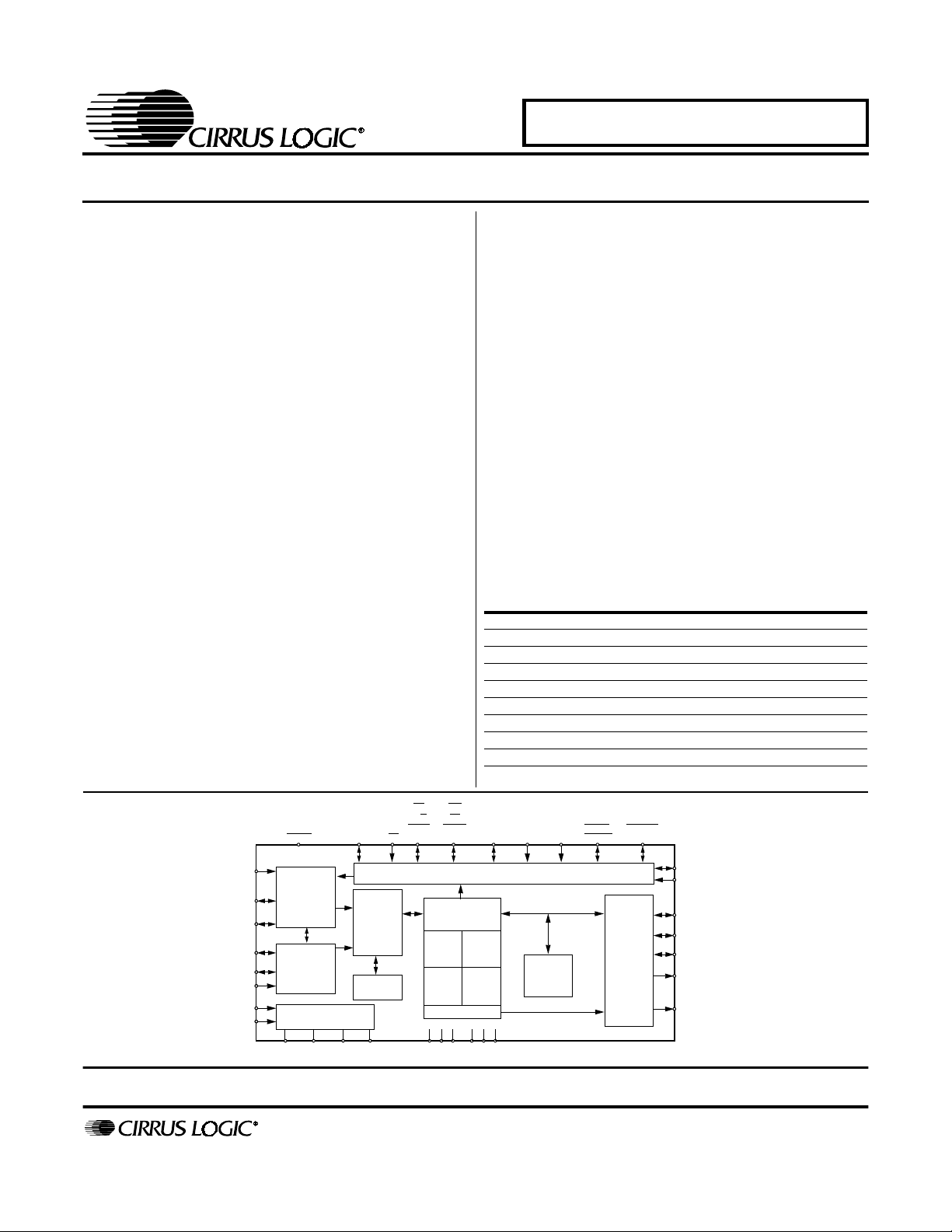
Compressed
Data Input
Interface
Digital
Audio
Input
Interface
PLL
Clock Manager
FILT1
FILT2 AGND
Preliminary Product Information
P.O. Box 17847, Austin, Texas 78760
(512) 445 7222 FAX: (512) 445 7581
http://www.cirrus.com
DATA7:0,
EMAD7:0,
GPIO7:0
Framer
Shifter
Input
Buffer
Controller
RAM Input
Buffer
VA
RD
WR
,
,
R/W,
EMOE,
CS
GPIO11
DSP Processing
Program
Memory
ROM
Program
Memory
DGND[3:1] VD[3:1]
SCDIO,
DS,
SCDOUT,
EMWR,
PSEL,
GPIO9
A0,
SCCLK
RAM
Output
Buffer
GPIO10
Parallel or Serial Host Interface
24-Bit
RAM
RAM
Data
Memory
ROM
Data
Memory
STC
A1,
SCDIN
ABOOT,
INTREQ
EXTMEM,
GPIO8
Output
Formatter
DD
DC
MCLK
SCLK
LRCLK
AUDATA[2.0]
XMT958/AUDATA3
This document contains information for a new product.
Cirrus Logic reserves the right to modify this product without notice.
Copyright Cirrus Logic, Inc. 2002
(All Rights Reserved)
MAR ‘02
DS339PP4
1

TABLE OF CONTENTS
1. CHARACTERISTICS AND SPECIFICATIONS ................................................................. 6
1.1 Absolute Maximum Ratings ........................................................................................ 6
1.2 Recommended Operating Conditions ......................................................................... 6
1.3 Digital D.C. Characteristics ......................................................................................... 6
1.4 Power Supply Characteristics ..................................................................................... 6
1.5 Switching Characteristics — RESET
1.6 Switching Characteristics — CLKIN ............................................................................ 7
1.7 Switching Characteristics — Intel
1.8 Switching Characteristics — Motorola
1.9 Switching Characteristics — SP
1.10 Switching Characteristics — I
1.11 Switching Characteristics — Digital Audio Input ..................................................... 16
1.12 Switching Characteristics — CMPDAT, CMPCLK .................................................. 18
1.13 Switching Characteristics — Parallel Data Input ..................................................... 18
1.14 Switching Characteristics — Digital Audio Output ................................................... 19
2. FAMILY OVERVIEW ....................................................................................................... 21
2.1 Multichannel Decoder Family of Parts ...................................................................... 21
3. TYPICAL CONNECTION DIAGRAMS ........................................................................... 24
3.1 Multiplexed Pins ........................................................................................................ 24
3.2 Termination Requirements ........................................................................................ 25
3.3 Phase Locked Loop Filter ......................................................................................... 25
4. POWER ........................................................................................................................... 25
4.1 Decoupling ................................................................................................................ 25
4.2 Analog Power Conditioning ....................................................................................... 25
CS49300 Family DSP
........................................................................ 7
®
Host Mode ........................................................... 8
®
I
2C®
Host Mode .................................................. 10
Control Port .......................................................... 12
Control Port ....................................................... 14
Contacting Cirrus Logic Support
For a complete listing of Direct Sales, Distributor, and Sales Representative contacts, visit the Cirrus Logic web site at:
http://www.cirrus.com/corporate/contacts
Dolby Digital, AC-3, Dolby Pro Logic, Dolby Pro Logic II, Dolby Surround, Surround EX, Virtual Dolby Digital, MLP and the “AAC” logo are trademarks
and the “Dolby Digital” logo, “Dolby Digital with Pro Logic II” logo, “Dolby” and the double-”D” symbol are registered trademarks of Dolby Laboratories
Licensing Corporation. DTS, DTS Digital Surround, DTS-ES Extended Surround, DTS Neo:6, and DTS Virtual 5.1 are trademarks and the “DTS”,
“DTS-ES”, “DTS Virtual 5.1” logos are registered trademarks of the Digital Theater Systems Corporation. The “MPEG Logo” is a registered trademark
of Philips Electronics N.V. Home THX Cinema and THX are registered trademarks of Lucasfilm Ltd. Surround EX is a jointly developed technology
of THX and Dolby Labs, Inc. AAC (Advanced Audio Coding) is an “MPEG-2-standard-based” digital audio compression algorithm (offering up 5.1
discrete decoded channels for this implementation) collaboratively developed by AT&T, the Fraunhofer Institute, Dolby Laboratories, and the Sony
Corporation. In regards to the MP3 capable functionality of the CS49300 Family DSP (via downloading of mp3_493xxx_vv.ld and mp3e_493xxx_vv.ld
application codes) the following statements are applicable: “Supply of this product conveys a license for personal, private and non-commercial use.
MPEG Layer-3 audio decoding technology licensed from Fraunhofer IIS and THOMSON Multimedia.” MLP and Meridian Lossless Packing are
registered trademarks of Meridian Audio Ltd. Harman VMAx is a registered trademark of Harman International. The LOGIC7 logo and LOGIC7 are
registered trademarks of Lexicon. SRS Circle Surround, and SRS TruSurround are trademarks of SRS Labs, Inc. The HDCD logo, HDCD, High
Definition Compatible Digital and Pacific Microsonics are either registered trademarks or trademarks of Pacific Microsonics, Inc. in the United States
and/or other countries. HDCD technology provided under license from Pacific Microsonics, Inc. This product’s software is covered by one or more of
the following in the United States: 5,479,168; 5,638,074; 5,640,161; 5,872,531; 5,808,574; 5,838,274; 5,854,600; 5,864,311; and in Australia:
669114; with other patents pending. Intel is a registered trademark of Intel Corporation. Motorola is a registered trademark of Motorola, Inc. I
registered trademark of Philips Semiconductor. Purchase of I
conveys a license under the Philips I2C Patent Rights to use those components in a standard I2C system. The “Cirrus Logic Logo” is a registered
trademark of Cirrus Logic, Inc. All other names are trademarks, registered trademarks, or service marks of their respective companies.
Preliminary product information describes products which are in production, but for which full characterization data is not yet available. Advance
product information describes products which are in development and subject to development changes. Cirrus Logic, Inc. has made best efforts to
ensure that the information contained in this document is accurate and reliable. However, the information is subject to change without notice and is
provided “AS IS” without warranty of any kind (express or implied). No responsibility is assumed by Cirrus Logic, Inc. for the use of this information,
nor for infringements of patents or other rights of third parties. This document is the property of Cirrus Logic, Inc. and implies no license under patents,
copyrights, trademarks, or trade secrets. No part of this publication may be copied, reproduced, stored in a retrieval system, or transmitted, in any
form or by any means (electronic, mechanical, photographic, or otherwise) without the prior written consent of Cirrus Logic, Inc. Items from any Cirrus
Logic web site or disk may be printed for use by the user. However, no part of the printout or electronic files may be copied, reproduced, stored in a
retrieval system, or transmitted, in any form or by any means (electronic, mechanical, photographic, or otherwise) without the prior written consent
of Cirrus Logic, Inc. The names of products of Cirrus Logic, Inc. or other vendors and suppliers appearing in this document may be trademarks or
service marks of their respective owners which may be registered in some jurisdictions. A list of Cirrus Logic, Inc. trademarks and service marks can
be found at http://www.cirrus.com.
2
C Components of Cirrus Logic, Inc., or one of its sublicensed Associated Companies
2
C is a
2 DS339PP4

CS49300 Family DSP
4.3 Ground ...................................................................................................................... 32
4.4 Pads ......................................................................................................................... 32
5. CLOCKING .....................................................................................................................32
6. CONTROL ......................................................................................................................32
6.1 Serial Communication .............................................................................................. 33
6.1.1 SPI Communication ...................................................................................... 33
2
6.1.2 I
6.1.3 INTREQ Behavior: A Special Case .............................................................. 39
6.2 Parallel Host Communication ................................................................................... 41
6.2.1 Intel Parallel Host Communication Mode ..................................................... 43
6.2.2 Motorola Parallel Host Communication Mode .............................................. 45
6.2.3 Procedures for Parallel Host Mode Communication .................................... 46
7. EXTERNAL MEMORY .................................................................................................... 48
7.1 Non-Paged Memory ................................................................................................. 49
7.2 Paged Memory ........................................................................................................ 49
8. BOOT PROCEDURE & RESET ..................................................................................... 52
8.1 Host Boot ..................................................................................................................52
8.1.1 Serial Download Sequence .......................................................................... 52
8.1.2 Parallel Download Sequence ....................................................................... 55
8.2 Autoboot ...................................................................................................................56
8.2.1 Autoboot INTREQ
8.3 Decreasing Autoboot Times Using GFABT Codes (Fast Autoboot) ......................... 59
8.3.1 Design Considerations when using GFABT Codes ...................................... 61
8.4 Internal Boot ............................................................................................................. 61
8.5 Application Failure Boot Message ............................................................................ 61
8.6 Resetting the CS493XX ............................................................................................ 61
8.7 External Memory Examples ...................................................................................... 63
8.7.1 Non-Paged Autoboot Memory ...................................................................... 63
8.7.2 32 Kilobyte Paged Autoboot Memory ........................................................... 64
8.8 CDB49300-MEMA.0 ................................................................................................. 65
9. HARDWARE CONFIGURATION ................................................................................... 67
10.DIGITAL INPUT & OUTPUT ........................................................................................... 67
10.1 Digital Audio Formats .............................................................................................. 67
10.1.1 I
10.1.2 Left Justified ............................................................................................... 67
10.1.3 Multichannel ............................................................................................... 67
10.2 Digital Audio Input Port ........................................................................................... 68
10.3 Compressed Data Input Port ................................................................................... 69
10.4 Byte Wide Digital Audio Data Input ......................................................................... 69
10.4.1 Parallel Delivery with Parallel Control ........................................................ 69
10.4.2 Parallel Delivery with Serial Control ........................................................... 70
10.5 Digital Audio Output Port ......................................................................................... 70
10.5.1 IEC60958 Output ........................................................................................ 71
11.HARDWARE CONFIGURATION ................................................................................... 72
11.1 Address Checking ................................................................................................... 72
11.2 Input Data Hardware Configuration ........................................................................ 72
11.2.1 Input Configuration Considerations ......................................................... 75
11.3 Output Data Hardware Configuration ...................................................................... 76
11.3.1 Output Configuration Considerations ........................................................ 78
11.4 Creating Hardware Configuration Messages .......................................................... 78
C Communication ...................................................................................... 35
Behavior ......................................................................... 57
2
S .............................................................................................................. 67
DS339PP4 3

12.PIN DESCRIPTIONS ....................................................................................................... 80
13.ORDERING INFORMATION............................................................................................ 85
14.PACKAGE DIMENSIONS ............................................................................................... 85
LIST OF FIGURES
Figure 1. RESET Timing ..................................................................................................................... 7
Figure 2. CLKIN with CLKSEL = VSS = PLL Enable .......................................................................... 7
Figure 3. Intel
Figure 4. Intel
Figure 5. Motorola
Figure 6. Motorola
Figure 7. SPI Control Port Timing ..................................................................................................... 13
Figure 8. I2C
Figure 9. Digital Audio Input Data, Master and Slave Clock Timing ................................................. 17
Figure 10. Serial Compressed Data Timing ...................................................................................... 18
Figure 11. Parallel Data Timing (when not in a parallel control mode) ............................................. 18
Figure 12. Digital Audio Output Data, Input and Output Clock Timing ............................................. 20
Figure 13. I
Figure 14. I
Figure 15. SPI Control ...................................................................................................................... 28
Figure 16. SPI Control with External Memory ................................................................................... 29
Figure 17. Intel
Figure 18. Motorola
Figure 19. SPI Write Flow Diagram .................................................................................................. 33
Figure 20. SPI Read Flow Diagram .................................................................................................. 34
Figure 21. SPI Timing ....................................................................................................................... 36
Figure 22. I2C® Write Flow Diagram ................................................................................................ 37
Figure 23. I2C® Read Flow Diagram ................................................................................................ 38
Figure 24. I2C® Timing ..................................................................................................................... 40
Figure 24. Intel Mode, One-Byte Write Flow Diagram ...................................................................... 44
Figure 25. Intel Mode, One-Byte Read Flow Diagram ...................................................................... 44
Figure 26. Motorola Mode, One-Byte Write Flow Diagram ............................................................... 45
Figure 27. Motorola Mode, One-Byte Read Flow Diagram ............................................................... 46
Figure 28. Typical Parallel Host Mode Control Write Sequence Flow Diagram ............................... 47
Figure 29. Typical Parallel Host Mode Control Read Sequence Flow Diagram ............................... 48
Figure 30. External Memory Interface .............................................................................................. 51
Figure 31. External Memory Read (16-bit address) ......................................................................... 51
Figure 32. External Memory Write (16-bit address) .......................................................................... 51
Figure 33. Typical Serial Boot and Download Procedure ................................................................. 53
Figure 34. Typical Parallel Boot and Download Procedure .............................................................. 54
Figure 35. Autoboot Timing Diagram ................................................................................................ 56
Figure 37. Autoboot INTREQ Behavior ............................................................................................57
Figure 36. Autoboot Sequence ......................................................................................................... 58
®
®
®
Control Port Timing ................................................................................................... 15
2C®
2C®
CS49300 Family DSP
Parallel Host Mode Read Cycle ................................................................................. 9
Parallel Host Mode Write Cycle ................................................................................. 9
®
Parallel Host Mode Read Cycle ........................................................................ 11
®
Parallel Host Mode Write Cycle ........................................................................ 11
Control ..................................................................................................................... 26
Control with External Memory ................................................................................. 27
®
Parallel Control Mode ............................................................................................ 30
®
Parallel Control Mode ..................................................................................... 31
4 DS339PP4

Figure 38. Fast Autoboot Sequence Using GFABT Codes ...............................................................60
Figure 39. Performing a Reset ..........................................................................................................62
Figure 40. Non-Paged Memory .........................................................................................................64
Figure 41. Example Contents of a Paged 32 Kilobytes External Memory (Total 256 Kilobytes) .......64
Figure 42. CDB49300-MEMA.0 Daughter Card for the CDB4923/30-REV-A.0 ................................66
Figure 43. I
Figure 44. Left Justified Format (Rising Edge Valid SCLK) ...............................................................68
Figure 45. Multichannel Format .........................................................................................................68
2
S Format ........................................................................................................................68
LIST OF TABLES
Table 1. PLL Filter Component Values .............................................................................................. 25
Table 2. Host Modes .......................................................................................................................... 32
Table 3. SPI Communication Signals................................................................................................. 33
Table 4. I
Table 5. Parallel Input/Output Registers ............................................................................................ 42
Table 6. Intel Mode Communication Signals...................................................................................... 43
Table 7. Motorola Mode Communication Signals .............................................................................. 45
Table 8. Memory Interface Pins ......................................................................................................... 49
Table 9. Boot Write Messages ........................................................................................................... 52
Table 10. Boot Read Messages......................................................................................................... 52
Table 11. Reduced Autoboot Times using GFABT8.LD, GFABT6.LD, and GFABT4.LD
on a CS493264-CL Rev. G DSP........................................................................................................ 59
Table 12. Memory Requirements for Example 5.1, 6.1 and 7.1 Channel Systems ........................... 63
Table 13. Digital Audio Input Port ...................................................................................................... 68
Table 14. Compressed Data Input Port.............................................................................................. 69
Table 15. Digital Audio Output Port.................................................................................................... 70
Table 16. MCLK/SCLK Master Mode Ratios...................................................................................... 71
Table 17. Output Channel Mapping ................................................................................................... 71
Table 18. Input Data Type Configuration
(Input Parameter A)............................................................................................................................ 73
Table 19. Input Data Format Configuration
(Input Parameter B)............................................................................................................................ 73
Table 20. Input SCLK Polarity Configuration
(Input Parameter C) ........................................................................................................................... 75
Table 21. Input FIFO Setup Configuration
(Input Parameter D) ........................................................................................................................... 75
Table 22. Output Clock Configuration
(Parameter A)..................................................................................................................................... 76
Table 23. Output Data Format Configuration
(Parameter B)..................................................................................................................................... 76
Table 24. Output MCLK Configuration
(Parameter C) .................................................................................................................................... 77
Table 25. Output SCLK Configuration
(Parameter D) .................................................................................................................................... 77
Table 26. Output SCLK Polarity Configuration
(Parameter E)..................................................................................................................................... 77
Table 27. Example Values to be Sent to CS493XX After Download or Soft Reset ........................... 79
2
C® Communication Signals ............................................................................................. 35
CS49300 Family DSP
DS339PP4 5
CS49300 Family DSP
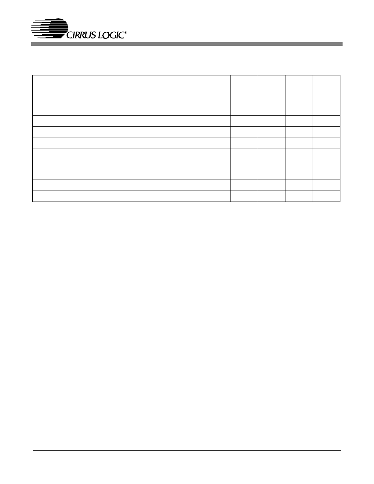
1. CHARACTERISTICS AND SPECIFICATIONS
1.1. Absolute Maximum Ratings
(AGND, DGND = 0 V; all voltages with respect to 0 V)
Parameter Symbol Min Max Unit
DC power supplies: Positive digital
Positive analog
||VA| – |VD||
Input current, any pin except supplies I
Digital input voltage V
Storage temperature T
CAUTION: Operation at or beyond these limits may result in permanent damage to the device. Normal operation
is not guaranteed at these extremes.
1.2. Recommended Operating Conditions
(AGND, DGND = 0 V; all voltages with respect to 0 V)
Parameter Symbol Min Typ Max Unit
DC power supplies: Positive digital
Positive analog
||VA| – |VD||
Ambient operating temperature T
VD
VA
in
IND
stg
VD
VA
–0.3
–0.3
-
-
2.75
2.75
0.3
10 mA
±
V
V
V
–0.3 3.63 V
–65 150
2.37
2.37
-
A
0-70°C
2.5
2.5
-
2.63
2.63
0.3
C
°
V
V
V
1.3. Digital D.C. Characteristics
(TA = 25°C; VA, VD[3:1] = 2.5 V±5%; measurements performed under static conditions.)
Parameter Symbol Min Typ Max Unit
High-level input voltage V
Low-level input voltage V
High-level output voltage at I
Low-level output voltage at I
= –2.0 mA V
O
= 2.0 mA V
O
Input leakage current I
IH
IL
OH
OL
in
2.0 - - V
--0.8V
VD×0.9 - - V
--VD
--1.0µA
1.4. Power Supply Characteristics
(TA = 25°C; VA, VD[3:1] = 2.5 V±5%; measurements performed under operating conditions)
Parameter Symbol Min Typ Max Unit
Power supply current: Digital operating: VD[3:1]
Analog operating: VA
-
-
200
1.7
0.11 V
×
310
4
mA
mA
6 DS339PP4
CS49300 Family DSP
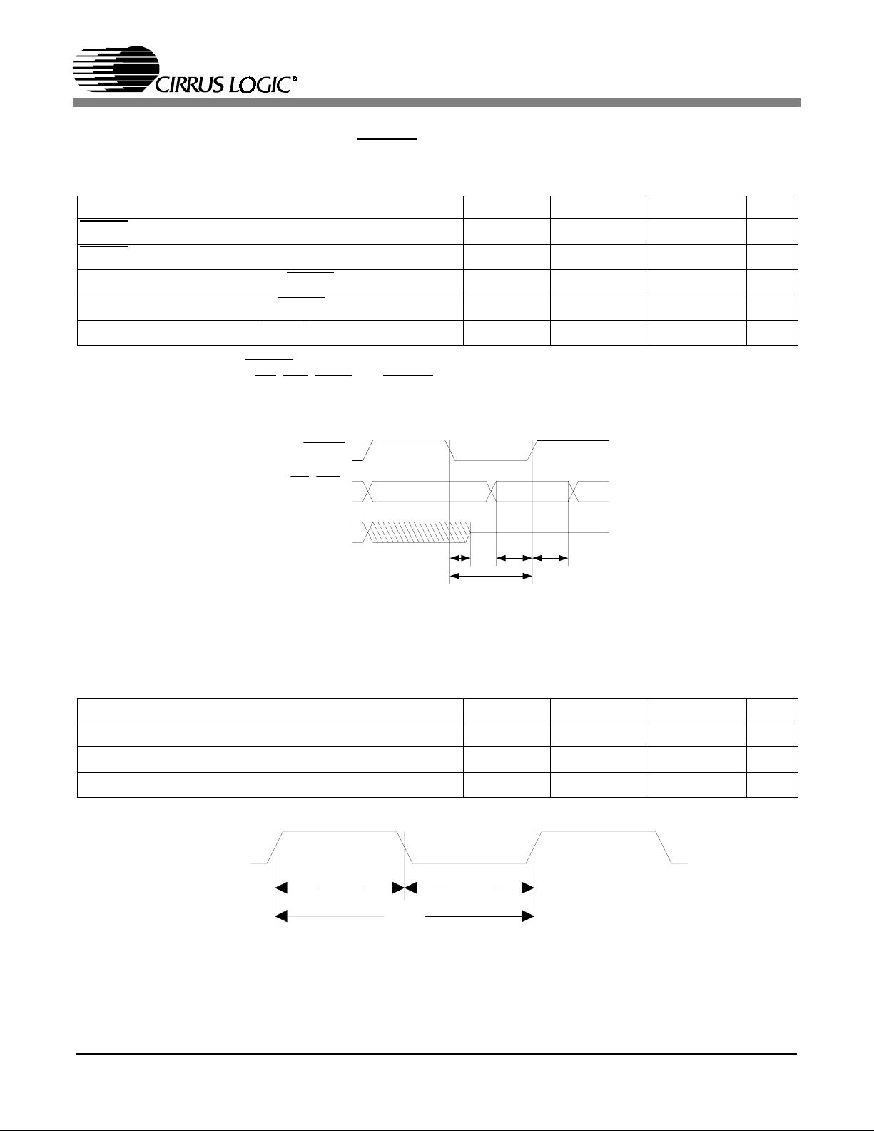
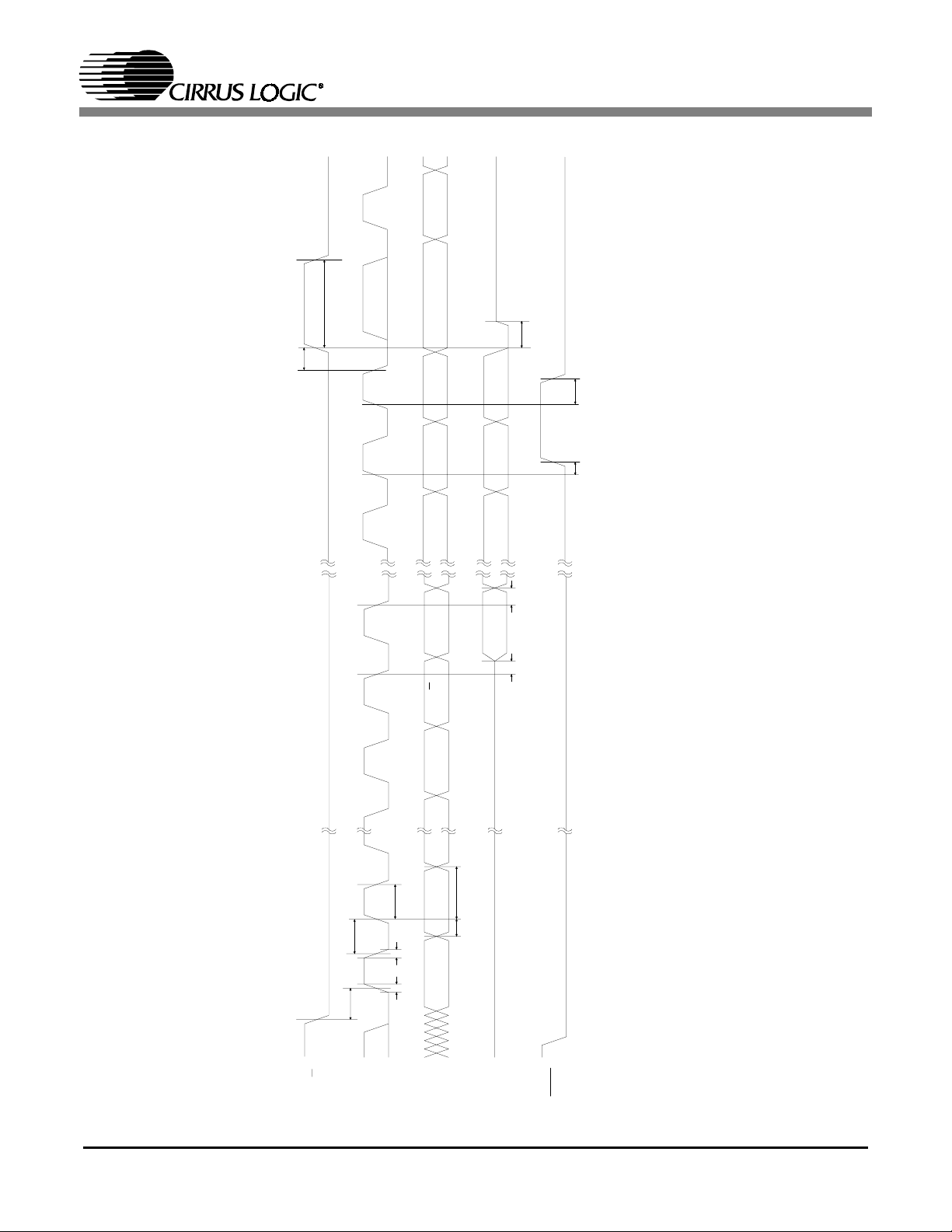
1.5. Switching Characteristics — RESET
(TA = 25°C; VA, VD[3:1] = 2.5 V±5%; Inputs: Logic 0 = DGND, Logic 1 = VD, CL = 20 pF)
Parameter Symbol Min Max Unit
RESET
RESET
minimum pulse width low (-CL) (Note 1)
minimum pulse width low (-IL) (Note 1)
All bidirectional pins high-Z after RESET
Configuration bits setup before RESET
Configuration bits hold after RESET
high
low (Note 2)
high
T
T
T
rst2z
T
rstsu
T
rsthld
rstl
rstl
100 -
530 -
-50ns
50 - ns
15 - ns
s
µ
s
µ
Notes: 1. The minimum RESET
resistors on the RD
pulse listed above is valid only when using the recommended pull-up/pull-down
, WR, PSEL and ABOOT mode pins. For Rev. D and older parts, pull-up/pull-down
resistors may be 4.7 k or 3.3 k. For Rev. E and newer parts, pull-up/pull-down resistors must be 3.3 k.
2. This specification is characterized but not production tested.
RESET
RD, W R,
PSEL, ABOOT
All Bidirectional
Pins
T
rst2z
T
rstl
T
rstsuTrsthld
Figure 1. RESET Timing
1.6. Switching Characteristics — CLKIN
(TA = 25°C; VA, VD[3:1] = 2.5 V±5%; Inputs: Logic 0 = DGND, Logic 1 = VD, CL = 20 pF)
Parameter Symbol Min Max Unit
CLKIN period for internal DSP clock mode T
CLKIN high time for internal DSP clock mode T
CLKIN low time for internal DSP clock mode T
clki
clkih
clkil
35 3800 ns
18 ns
18 ns
CLKIN
T
clkih
T
clki
Figure 2. CLKIN with CLKSEL = VSS = PLL Enable
DS339PP4 7
T
clkil
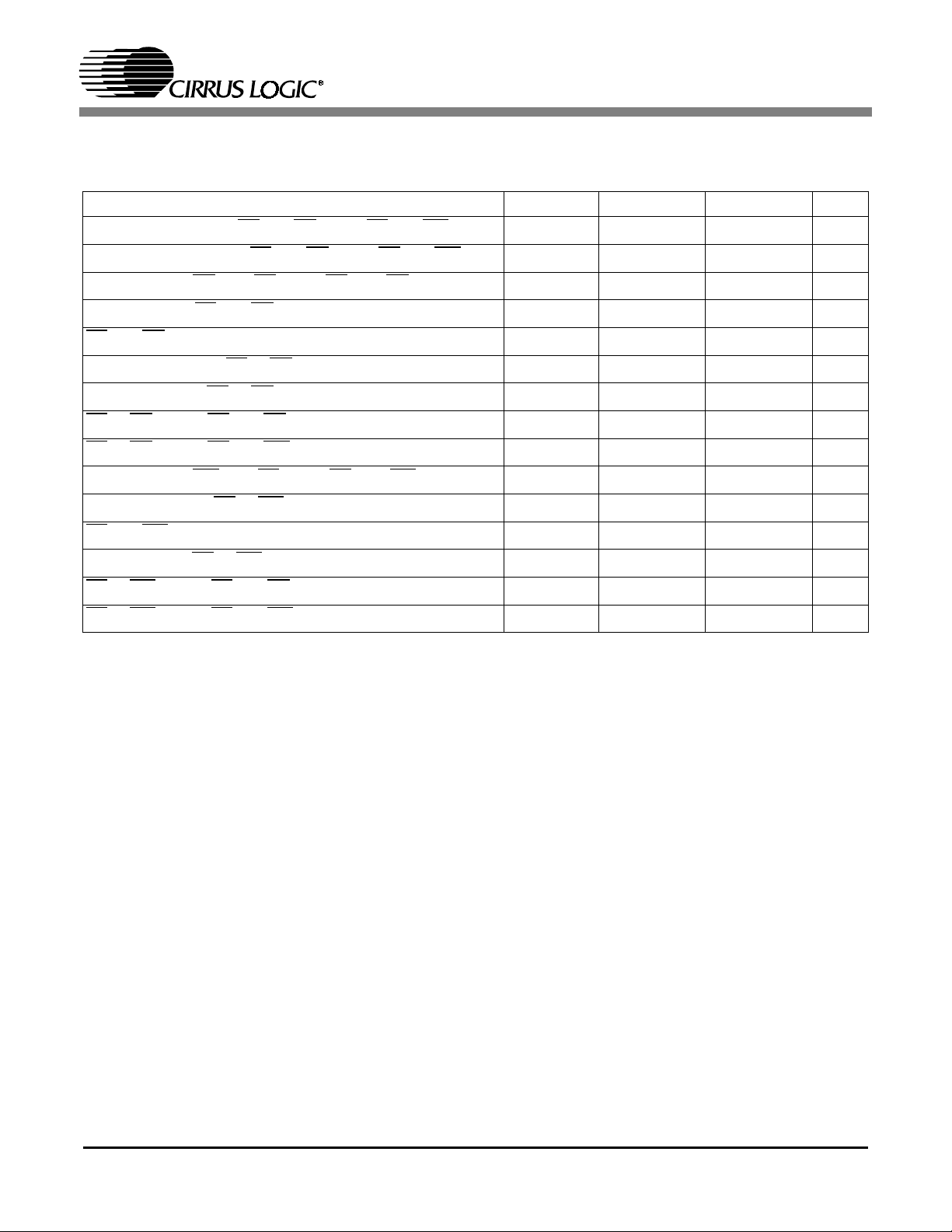
1.7. Switching Characteristics — Intel® Host Mode
CS49300 Family DSP
(TA = 25°C; VA, VD[3:1] = 2.5 V±5%; Inputs: Logic 0 = DGND, Logic 1 = VD, CL = 20 pF)
Parameter Symbol Min Max Unit
Address setup before CS and RD low or CS and WR low
Address hold time after CS
Delay between RD
Data valid after CS
and RD low for read (Note 1)
CS
then CS low or CS then RD low
and RD low (Note 3)
Data hold time after CS
Data high-Z after CS
or RD high to CS and RD low for next read (Note 1)
CS
or RD high to CS and WR low for next write (Note 1)
CS
Delay between WR
then CS low or CS then WR low
Data setup before CS
CS
and WR low for write (Note 1)
Data hold after CS
or WR high to CS and RD low for next read (Note 1)
CS
or WR high to CS and WR low for next write (Note 1)
CS
or WR high
and RD low or CS and WR low
or RD high
or RD high (Note 2)
or WR high
T
T
T
T
T
T
T
T
T
T
T
T
T
T
T
ias
iah
icdr
idd
irpw
idhr
idis
ird
irdtw
icdw
idsu
iwpw
idhw
iwtrd
iwd
5-ns
5-ns
0
-21ns
DCLKP + 10 - ns
5-ns
-22ns
2*DCLKP + 10 - ns
2*DCLKP + 10 - ns
0
20 - ns
DCLKP + 10 - ns
5-ns
2*DCLKP + 10 - ns
2*DCLKP + 10 - ns
∞
∞
ns
ns
Notes: 1. Certain timing parameters are normalized to the DSP clock, DCLKP, in nanoseconds. DCLKP =
1/DCLK. The DSP clock can be defined as follows:
External CLKIN Mode:
DCLK == CLKIN/4 before and during boot
DCLK == CLKIN after boot
Internal Clock Mode:
DCLK == 10MHz before and during boot, i.e. DCLKP == 100ns
DCLK == 65 MHz after boot, i.e. DCLKP == 15.4ns
It should be noted that DCLK for the internal clock mode is application specific. The application code
users guide should be checked to confirm DCLK for the particular application.
2. This specification is characterized but not production tested. A 470 ohm pull-up resistor was used for
characterization to minimize the effects of external bus capacitance.
3. See T
from Intel Host Mode in Table 6 on page 43
idd
8 DS339PP4
A1:0
DATA7:0
CS
WR
RD
A1:0
DATA7:0
CS
RD
CS49300 Family DSP
T
ia h
T
ias
T
icdr
Figure 3. Intel® Parallel Host Mode Read Cycle
T
iah
T
ias
T
icdw
T
idd
T
T
irpw
iw p w
idhr
T
idis
T
ird
T
idh w
T
idsu
T
iw d
T
irdtw
T
iw trd
T
WR
Figure 4. Intel® Parallel Host Mode Write Cycle
DS339PP4 9
CS49300 Family DSP
1.8. Switching Characteristics — Motorola® Host Mode
(TA = 25°C; VA, VD[3:1] = 2.5 V±5%; Inputs: Logic 0 = DGND, Logic 1 = VD, CL = 20 pF)
Parameter Symbol Min Max Unit
Address setup before CS and DS low
Address hold time after CS
Delay between DS
Data valid after CS
then CS low or CS then DS low
and RD low with R/W high (Note 3)
and DS low
T
T
T
T
mas
mah
mcdr
mdd
5-ns
5-ns
0
-21ns
∞
ns
and DS low for read (Note 1)
CS
Data hold time after CS
Data high-Z after CS
or DS high to CS and DS low for next read (Note 1)
CS
CS
or DS high to CS and DS low for next write (Note 1)
Delay between DS
Data setup before CS
CS
and DS low for write (Note 1)
setup before CS AND DS low
R/W
hold time after CS or DS high
R/W
Data hold after CS
or DS high to CS and DS low with R/W high for next read
CS
or DS high after read
or DS high low after read (Note 2)
then CS low or CS then DS low
or DS high
or DS high
T
mrpw
T
mdhr
T
mdis
T
T
mrdtw
T
mcdw
T
mdsu
T
mwpw
T
mrwsu
T
mrwhld
T
mdhw
T
mwtrd
mrd
DCLKP + 10 - ns
5-ns
-22ns
2*DCLKP + 10 - ns
2*DCLKP + 10 - ns
0
∞
20 - ns
DCLKP + 10 - ns
5-ns
5-ns
5-ns
2*DCLKP + 10 - ns
(Note 1)
CS
or DS high to CS and DS low for next write (Note 1)
T
mwd
2*DCLKP + 10 - ns
Notes: 1. Certain timing parameters are normalized to the DSP clock, DCLKP, in nanoseconds. DCLKP =
1/DCLK. The DSP clock can be defined as follows:
External CLKIN Mode:
DCLK == CLKIN/4 before and during boot
DCLK == CLKIN after boot
ns
Internal Clock Mode:
DCLK == 10MHz before and during boot, i.e. DCLKP == 100ns
DCLK == 65 MHz after boot, i.e. DCLKP == 15.4ns
It should be noted that DCLK for the internal clock mode is application specific. The application code
users guide should be checked to confirm DCLK for the particular application.
2. This specification is characterized but not production tested. A 470 ohm pull-up resistor was used for
characterization to minimize the effects of external bus capacitance.
3. See T
from Motorola Host Mode in Table 7 on page 45
mdd
10 DS339PP4
A1:0
DATA7:0
CS
R/W
DS
T
T
mrwsu
mas
T
mah
T
mdd
T
mrpw
mdhr
T
mrd
T
mdis
T
T
mcdr
Figure 5. Motorola® Parallel Host Mode Read Cycle
CS49300 Family DSP
T
mrwhld
T
mrdtw
A1:0
DATA7:0
CS
R/W
DS
T
mas
T
mah
T
T
mcdw
T
mrwsu
mdsu
T
mdhw
T
mwpw
T
mwd
Figure 6. Motorola® Parallel Host Mode Write Cycle
T
mrwhld
T
mwtrd
DS339PP4 11
CS49300 Family DSP
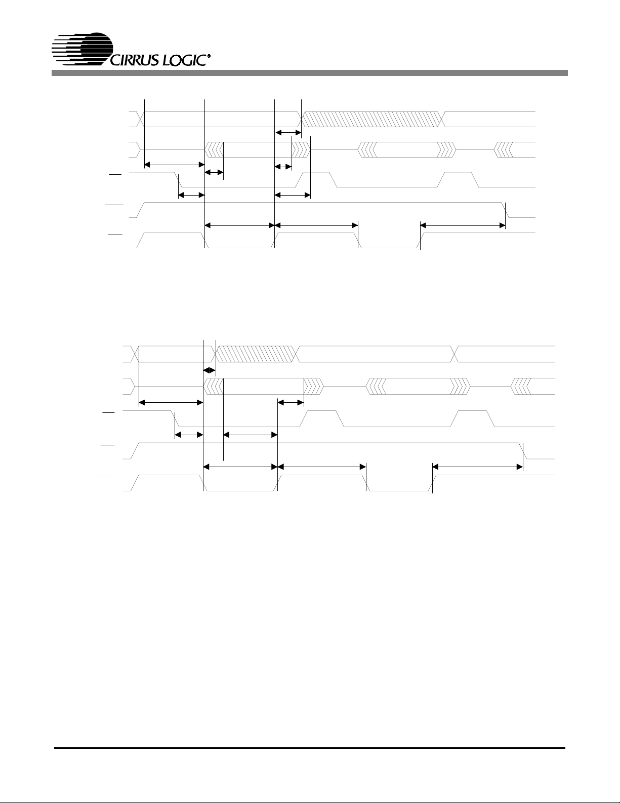
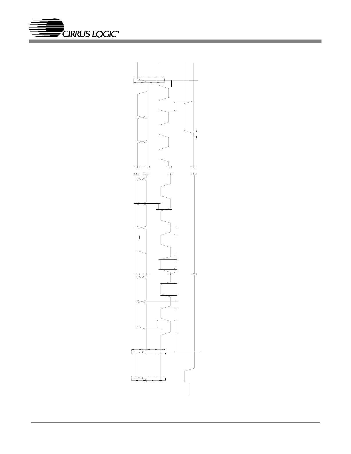
1.9. Switching Characteristics — SPI Control Port
(TA = 25°C; VA, VD[3:1] = 2.5 V±5%; Inputs: Logic 0 = DGND, Logic 1 = VD, CL = 20 pF)
Parameter Symbol Min Max Units
SCCLK clock frequency (Note 1) f
CS
falling to SCCLK rising t
Rise time of SCCLK line (Note 7) t
Fall time of SCCLK lines (Note 7) t
SCCLK low time t
SCCLK high time t
Setup time SCDIN to SCCLK rising t
Hold time SCCLK rising to SCDIN (Note 2) t
Transition time from SCCLK to SCDOUT valid (Note 3) t
Time from SCCLK rising to INTREQ
Rise time for INTREQ
Hold time for INTREQ
from SCCLK rising (Note 5, 7) t
Time from SCCLK falling to CS
rising (Note 4) t
(Note 4) t
rising t
High time between active CS
Time from CS
rising to SCDOUT high-Z (Note 7) t
sck
css
r
f
scl
sch
cdisu
cdih
scdov
scrh
rr
scrl
sccsh
t
csht
cscdo
20 - ns
150 - ns
150 - ns
50 - ns
50 - ns
20 - ns
200 - ns
- 2000 kHz
-50ns
-50ns
-40ns
- 200 ns
- (Note 6) ns
0-ns
20 ns
Notes: 1. The specification f
aware that the actual maximum speed of the communication port may be limited by the software. The
relevant application code user’s manual should be consulted for the software speed limitations.
2. Data must be held for sufficient time to bridge the 50 ns transition time of SCCLK.
3. SCDOUT should
4. INTREQ
goes high only if there is no data to be read from the DSP at the rising edge of SCCLK for the
second-to-last bit of the last byte of data during a read operation as shown.
5. If INTREQ
goes high as indicated in (Note 4), then INTREQ is guaranteed to remain high until the next
rising edge of SCCLK. If there is more data to be read at this time, INTREQ
this condition as a new read transaction. Raise chip select to end the current read transaction and then
drop it, followed by the 7-bit address and the R/W
6. With a 4.7k Ohm pull-up resistor this value is typically 215ns. As this pin is open drain adjusting the pull
up value will affect the rise time.
7. This time is by design and not tested.
indicates the maximum speed of the hardware. The system designer should be
sck
be sampled during this time period.
not
goes active low again. Treat
bit (set to 1 for a read) to start a new read transaction.
12 DS339PP4
CS49300 Family DSP
A6
csht
t
sccsh
t
7
6
5
LSB
tri-sta te
cscdo
t
scrl
LSB
t
scrh
t
scl
t
css
t
scdov
t
0
7
6
2
1
0
sch
t
t
t
MSB
R/W
MSB
scdov
t
Figure 7. SPI Control Port Timing
A0A6 A5
cdih
t
cdisu
t
f
r
CS
SCCLK
SCDIN
SCDOUT
IN T R E Q
DS339PP4 13

CS49300 Family DSP
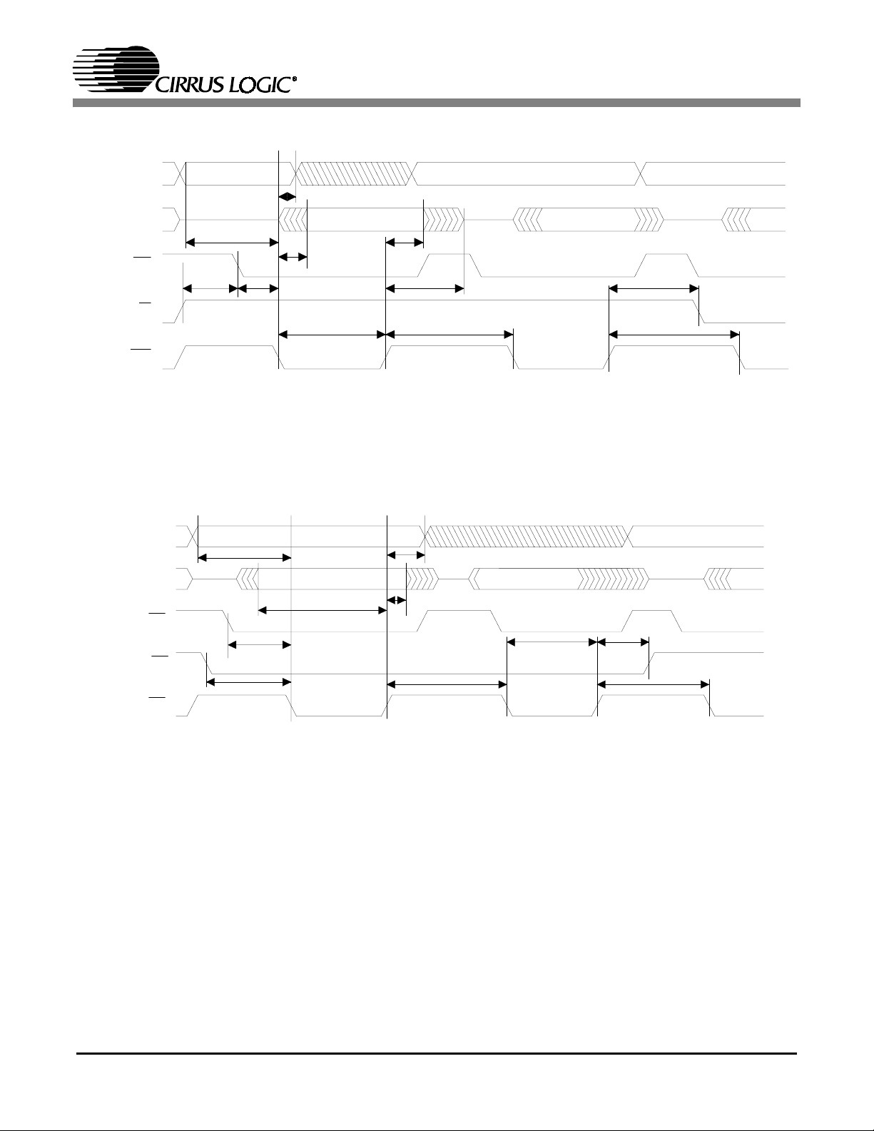
1.10. Switching Characteristics — I
2
C® Control Port
(TA = 25°C; VA, VD[3:1] = 2.5 V±5%; Inputs: Logic 0 = DGND, Logic 1 = VD, CL = 20 pF)
Parameter Symbol Min Max Units
SCCLK clock frequency (Note 1) f
Bus free time between transmissions t
Start-condition hold time (prior to first clock pulse) t
Clock low time t
Clock high time t
SCDIO setup time to SCCLK rising t
SCDIO hold time from SCCLK falling (Note 2) t
Rise time of SCCLK (Note 3), (Note 7) t
Fall time of SCCLK (Note 7) t
Time from SCCLK falling to CS493XX ACK t
Time from SCCLK falling to SCDIO valid during read operation t
Time from SCCLK rising to INTREQ
Hold time for INTREQ
from SCCLK rising (Note 5) t
Rise time for INTREQ
rising (Note 4) t
(Note 6) t
Setup time for stop condition t
scl
buf
hdst
low
high
sud
hdd
r
f
sca
scsdv
scrh
scrl
rr
susp
4.7
4.0
1.2
1.0
250 ns
4.7
400 kHz
s
µ
s
µ
s
µ
s
µ
0
s
µ
50 ns
300 ns
40 ns
40 ns
200 ns
0ns
** ns
s
µ
Notes:. 1. The specification f
aware that the actual maximum speed of the communication port may be limited by the software. The
relevant application code user’s manual should be consulted for the software speed limitations.
2. Data must be held for sufficient time to bridge the 300-ns transition time of SCCLK. This hold time is by
design and not tested.
3. This rise time is
shorter
Section 6.1, “Serial Communication” on page 33.
4. INTREQ
goes high only if there is no data to be read from the DSP at the rising edge of SCCLK for the
last data bit of the last byte of data during a read operation as shown.
5. If INTREQ
goes high as indicated in Note 8, then INTREQ is guaranteed to remain high until the next
rising edge of SCCLK. If there is more data to be read at this time, INTREQ
this condition as a new read transaction. Send a new start condition followed by the 7-bit address and
the R/W
bit (set to 1 for a read). This time is by design and is not tested.
6. With a 4.7k Ohm pull-up resistor this value is typically 215ns. As this pin is open drain adjusting the pull
up value will affect the rise time.
7. This time is by design and not tested.
indicates the maximum speed of the hardware. The system designer should be
scl
than that recommended by the I2C specifications. For more information, see
goes active low again. Treat
14 DS339PP4
CS49300 Family DSP
stop
8
ACK
7
LSB
0
MSB
scsdv
t
8
ACK
7
R/W
6
A0
t
scrl
susp
t
scrh
t
sca
t
Control Port Timing
®
C
2
f
t
r
t
Figure 8. I
1
A5
0
A6
sud
t
start
buf
t
stop
SCDIO
high
t
hdd
t
low
t
hdst
t
SCCLK
INTREQ
DS339PP4 15
CS49300 Family DSP
1.11. Switching Characteristics — Digital Audio Input
(TA = 25°C; VA, VD[3:1] = 2.5 V±5%; Inputs: Logic 0 = DGND, Logic 1 = VD, CL = 20 pF)
Parameter Symbol Min Max Unit
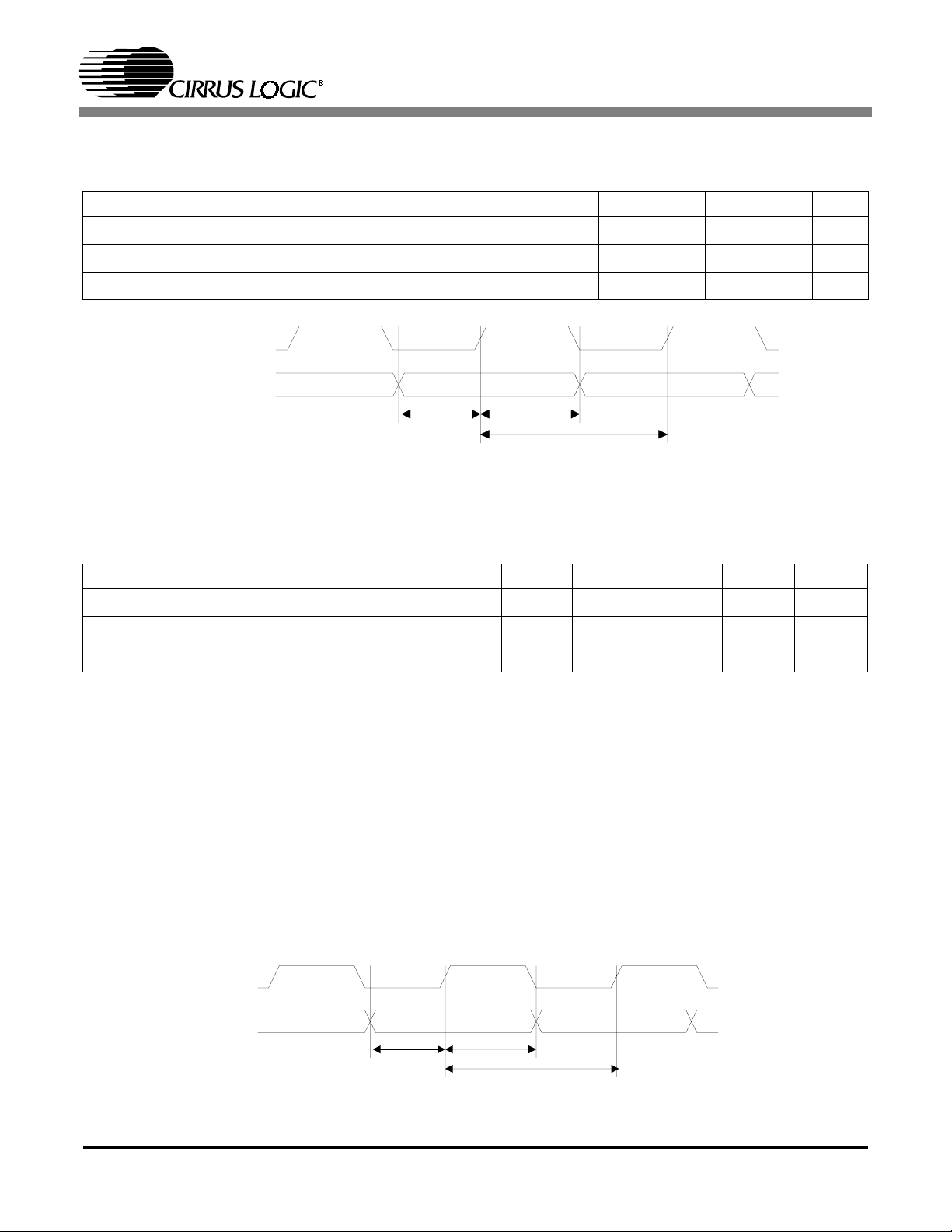
SCLKN1(2) period for both Master and Slave mode (Note 1) T
sclki
SCLKN1(2) duty cycle for Master and Slave mode (Note 1) 45 55 %
Master Mode (Note 1, 2)
LRCLKN1(2) delay after SCLKN1(2) transition (Note 3) T
SDATAN1(2) setup to SCLKN1(2) transition (Note 4) T
SDATAN1(2) hold time after SCLKN1(2) transition (Note 4) T
lrds
sdsum
sdhm
Slave Mode (Note 5)
Time from active edge of SCLKN1(2) to LRCLKN1(2) transition T
Time from LRCLKN1(2) transition to SCLKN1(2) active edge T
SDATAN1(2) setup to SCLKN1(2) transition (Note 4) T
SDATAN1(2) hold time after SCLKN1(2) transition (Note 4) T
stlr
lrts
sdsus
sdhs
Notes: 1. Master mode timing specifications are characterized, not production tested.
2. Master mode is defined as the CS493XX driving LRCLKN1(2) and SCLKN1(2). Master or Slave mode
can be programmed.
3. This timing parameter is defined from the non-active edge of SCLKN1(2). The active edge of
SCLKN1(2) is the point at which the data is valid.
4. This timing parameter is defined from the active edge of SCLKN1(2). The active edge of SCLKN1(2) is
the point at which the data is valid.
5. Slave mode is defined as SCLKN1(2) and LRCLKN1(2) being driven by an external source.
40 - ns
-10ns
10 - ns
5-ns
10 - ns
10 - ns
5-ns
5-ns
16 DS339PP4
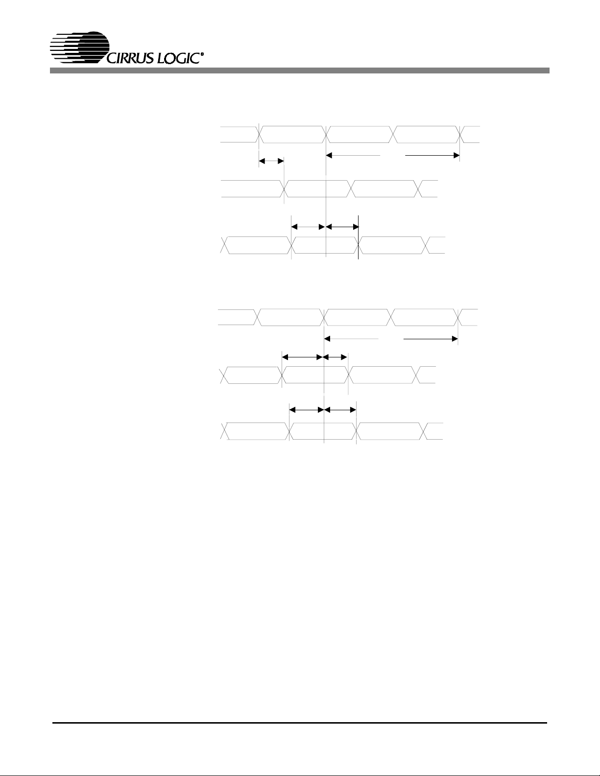
SCLKN1
SCLKN2
LRCLKN1
LRCLKN2
SDATAN1
SDATAN2
SCLKN1
SCLKN2
LRCLKN1
LRCLKN2
MASTER MODE
T
lrds
T
sdsu mTsdhm
SLAVE MODE
T
lrts
T
stlr
CS49300 Family DSP
T
sclki
T
sclki
T
sdsus
T
sdhs
SDATAN1
SDATAN2
Figure 9. Digital Audio Input Data, Master and Slave Clock Timing
DS339PP4 17
CS49300 Family DSP
1.12. Switching Characteristics — CMPDAT, CMPCLK
(TA = 25°C; VA, VD[3:1] = 2.5 V±5%; Inputs: Logic 0 = DGND, Logic 1 = VD, CL = 20 pF)
Parameter Symbol Min Max Unit
Serial compressed data clock CMPCLK period T
CMPDAT setup before CMPCLK high T
CMPDAT hold after CMPCLK high T
CMPCLK
CMPDAT
cmpclk
cmpsu
cmphld
-27MHz
5-ns
3-ns
T
cm psu
T
cm p clk
T
cmp hld
Figure 10. Serial Compressed Data Timing
1.13. Switching Characteristics — Parallel Data Input
(TA = 25°C; VA, VD[3:1] = 2.5 V±5%; Inputs: Logic 0 = DGND, Logic 1 = VD, CL = 20 pF)
Parameter Symbol Min Max Unit
CMPCLK Period T
DATA[7:0] setup before CMPCLK high T
DATA[7:0] hold after CMPCLK high T
cmpclk
cmpsu
cmphld
Notes: 1. Certain timing parameters are normalized to the DSP clock, DCLK, in nanoseconds. The DSP clock can
be defined as follows:
External CLKIN Mode:
DCLK == CLKIN/4 before and during boot
DCLK == CLKIN after boot
Internal Clock Mode:
DCLK == 10MHz before and during boot, i.e. DCLK == 100ns
DCLK == 65 MHz after boot, i.e. DCLK == 15.4ns
4*DCLK + 10 ns
10 ns
10 ns
It should be noted that DCLK for the internal clock mode is application specific. The application code
users guide should be checked to confirm DCLK for the particular application.
CMPCLK
DATA[7:0]
T
cmpsu
T
cmpclk
T
cmphld
Figure 11. Parallel Data Timing (when not in a parallel control mode)
18 DS339PP4

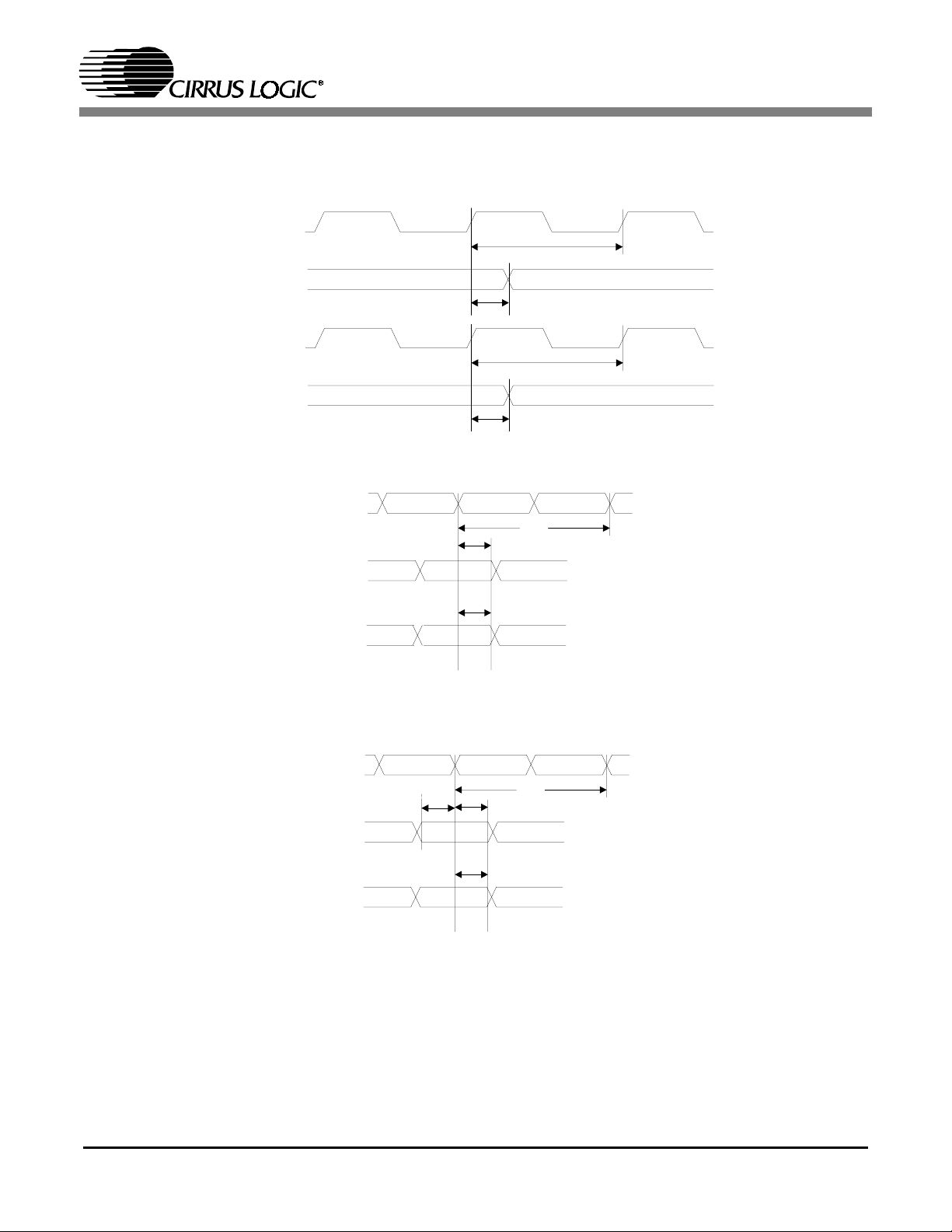
1.14. Switching Characteristics — Digital Audio Output
CS49300 Family DSP
(TA = 25°C; VA, VD[3:1] = 2.5 V±5%; Inputs: Logic 0 = DGND, Logic 1 = VD, CL = 20 pF)
Parameter Symbol Min Max Unit
MCLK period (Note 1) T
mclk
40 - ns
MCLK duty cycle (Note 1) 40 60 %
SCLK period for Master or Slave mode (Note 2) T
sclk
40 - ns
SCLK duty cycle for Master or Slave mode (Note 2) 45 55 %
Master Mode (Note 2, 3)
SCLK delay from MCLK rising edge, MCLK as an input T
SCLK delay from MCLK rising edge, MCLK as an output T
LRCLK delay from SCLK transition (Note 4) T
AUDATA2–0 delay from SCLK transition (Note 4) T
sdmi
sdmo
lrds
adsm
–5 10 ns
15 ns
10 ns
10 ns
Slave Mode (Note 5)
Time from active edge of SCLKN1(2) to LRCLKN1(2) transition T
Time from LRCLKN1(2) transition to SCLKN1(2) active edge T
AUDATA2–0 delay from SCLK transition (Note 4, 6) T
stlr
lrts
adss
10 - ns
10 - ns
15 ns
Notes: 1. MCLK can be an input or an output. These specifications apply for both cases.
2. Master mode timing specifications are characterized, not production tested.
3. Master mode is defined as the CS493XX driving both SCLK and LRCLK. When MCLK is an input, it is
divided to produce SCLK and LRCLK.
4. This timing parameter is defined from the non-active edge of SCLK. The active edge of SCLK is the
point at which the data is valid.
5. Slave mode is defined as SCLK and LRCLK being driven by an external source.
6. This specification is characterized, not production tested.
DS339PP4 19
MCLK (Input)
SCLK (Output)
MCLK (Output)
SCLK (Output)
SCLK
LRCLK
T
sdmi
T
sdmo
MASTER MODE
T
sclk
T
lrds
CS49300 Family DSP
T
mclk
T
mclk
AUDATA2:0
SCLK
LRCLK
AUDATA2:0
T
adsm
SLAVE MODE
T
T
lrts
T
adss
sclk
T
stlr
Figure 12. Digital Audio Output Data, Input and Output Clock Timing
20 DS339PP4

CS49300 Family DSP
2. FAMILY OVERVIEW
The CS49300 family contains system on a chip
solutions for multichannel audio decompression
and digital signal processing. The CS49300 family
is split into 4 sub-families targeted at the DVD,
broadcast and audio/video receiver (AVR), and
effects and post processing markets.
This document focuses on the electrical features
and characteristics of these parts. Different features
are described from a hardware design perspective.
It should be understood that not all of the features
portrayed in this document are supported by all of
the versions of application code available. The
application code user’s guides should be consulted
to confirm which hardware features are supported
by the software.
The parts use a combination of internal ROM and
RAM. Depending on the application being used, a
download of application software may be required
each time the part is powered up. This document
uses “download” and “code load” interchangeably.
These terms should be interpreted as meaning the
transfer of application code into the internal
memory of the part from either an external
microcontroller or through the autoboot procedure.
2.1. Multichannel Decoder Family of Parts
CS49300 - DVD Audio Decoder. The CS49300
device is targeted at audio decoding in the DVD via
ES or PES in a serial or parallel bursty fashion for
MLP or for DVD Audio Pack Layer Support. (All
the other decoding/processing algorithms listed
below require delivery of PCM or IEC61937packed compressed data via I2S or LJ formatted
digital audio to the CS49300). Specifically the
CS49300 will support all of the following
decoding/processing standards:
• Meridian Lossless Packing™ (MLP™)* (for ES
and PES data delivery only)
• DVD Audio Pack Layer Support* (for ES and
PES data delivery only)
• Dolby Digital™ (AC-3™) with
Dolby Pro Logic
™
• Dolby Digital™ with Dolby Pro Logic™ plus
Cirrus Extra Surround
• Dolby Digital™ with Dolby Pro Logic II
™
™
• Dolby Digital™ with Dolby Pro Logic II™ plus
Cirrus Extra Surround
• Virtual Dolby Digital
™
™
• MPEG-2, Advanced Audio Coding Algorithm
(AAC)
• MPEG Multichannel
• MPEG Multichannel with Dolby Pro Logic II
™
• MPEG Multichannel plus Cirrus Extra
Surround
™
• MPEG-1, Layer 3 (MP3)
• DTS Digital Surround
™
• DTS Digital Surround™ with
Dolby Pro Logic II
™
• DTS Digital Surround™ plus Cirrus Extra
Surround
• DTS-ES Extended Surround
™
™
(DTS-ES
Discrete 6.1 & Matrix 6.1)
• DTS Neo:6
™
• LOGIC5® (5.1 Channel, Max Fs=48kHz and
LOGIC7® (7.1 Channel, Max Fs=96kHz)
• VMAx VirtualTheater® (Virtual Dolby Digital)
• SRS TruSurround™ (Virtual Dolby Digital and
DTS Virtual 5.1™ Versions)
• SRS Circle Surround™ I/II
• HDCD
®
• Cirrus P.D.F. (Dolby Pro Logic 2Fs Decoder
and PCM Upsampler)
• Cirrus PL2_2FS (Dolby Pro Logic II 2Fs
Decoder and PCM Upsampler)
Please refer to the CS4932x/CS49330 Part Matrix
vs. Code Matrix (PDF) document available from
the CS49300 Web Site Page for the latest listing of
audio decoding/processing algorithms. The part
DS339PP4 21

CS49300 Family DSP
will also support PES layer decode for audio/video
synchronization and DVD Audio Pack layer
support. The CS49300 will support all of the above
decoding and PCM processing standards.
CS4931X - Broadcast Sub-family. The CS4931X
sub-family is targeted at audio decoding in the
broadcast markets in systems such as digital TV,
HDTV, set-top boxes and digital audio broadcast
units (digital radios). Specifically the CS4931X
sub-family will support the following decode
standards:
• Dolby Digital™ (AC-3™) with Dolby Pro
™
Logic
• MPEG-2, Advanced Audio Coding Algorithm
(AAC)
• MPEG-1, Layers 1, 2 Stereo
• MPEG-1, Layers 3 (MP3) Stereo
• MPEG-2, Layer 2 Stereo
• MPEG-2, Layer 3 (MP3) Stereo
The part will also support PES layer decode for
audio/video synchronization. The CS49310 will
support all of the above decode standards while
other parts in the CS4931X sub-family will decode
subsets of the above audio decoding standards.
• Dolby Digital™ with Dolby Pro Logic II™ plus
Cirrus Extra Surround
• Virtual Dolby Digital
™
™
• MPEG-2, Advanced Audio Coding Algorithm
(AAC)
• MPEG Multichannel
• MPEG Multichannel with Dolby Pro Logic II
™
• MPEG Multichannel plus Cirrus Extra
Surround
™
• MPEG-1, Layer 3 (MP3)
• DTS Digital Surround
™
• DTS Digital Surround™ with
Dolby Pro Logic II
™
• DTS Digital Surround™ plus Cirrus Extra
Surround
• DTS-ES Extended Surround
™
™
(DTS-ES
Discrete 6.1 & Matrix 6.1)
• DTS Neo:6
™
• LOGIC5® (5.1 Channel, Max Fs=48kHz and
LOGIC7® (7.1 Channel, Max Fs=96kHz)
• VMAx VirtualTheater® (Virtual Dolby Digital)
• SRS TruSurround™ (Virtual Dolby Digital and
DTS Virtual 5.1™ Versions)
CS4932X - Audio/Video Receiver (AVR) Subfamily. The CS4932X sub-family is targeted at
audio decoding in the audio/video receiver
markets. Typical applications will include
amplifiers with integrated decoding capability,
outboard decoder pre-amplifiers, car radios and
• SRS Circle Surround™ I/II
• HDCD
®
• Cirrus P.D.F. (Dolby Pro Logic 2Fs Decoder
and PCM Upsampler)
• Cirrus PL2_2FS (Dolby Pro Logic II 2Fs
Decoder and PCM Upsampler)
any system where the compressed audio is received
in an IEC61937 format. Specifically the CS4932X
sub-family will support the following decode
standards:
The CS49326 will support all of the above decode
standards while other parts in the CS4932X subfamily will decode subsets of the above audio
decoding standards.
• Dolby Digital™ (AC-3™) with
Dolby Pro Logic
™
Except for the CS49329 which offers AAC support
this subfamily will offer integrated ROM support
• Dolby Digital™ with Dolby Pro Logic™ plus
Cirrus Extra Surround
• Dolby Digital™ with Dolby Pro Logic II
22 DS339PP4
™
™
for the AC-3 code, DTS code, Cirrus Original
Surround code and DTS tables. The CS49329 will

CS49300 Family DSP
require an external download for all applications
but will still support the DTS tables on chip.
CS49330 - General Purpose, Car Audio
Processor, PCM Effects & Multichannel PostProcessing Device. The CS49330 sub-family is
targeted at any system that may require post
processing or multichannel effects processing, a
general purpose MPEG Stereo, MPEG
Multichannel, MP3, decoder or PCM effects
processor or mixer, or for car audio applications.
Typical applications will include multichannel
amplifiers, outboard pre-amplifiers, HDTVs and
car radios. Specifically the CS49330 sub-family
will support the following:
• Cirrus Digital Post-Processor, Home THX
Cinema® and THX Surround EX™ 5.1 and 7.1
Channel Post-Processors
• Any general purpose application which only
requires MPEG Multichannel; MPEG-1, Layer
3; MPEG-2, Layer 3*, or C.O.S. PCM Effects
Processor. (MPEG-1, Layer 3 and MPEG-2,
Layer 3 are only available for applications
where serial or parallel bursty elementary
stream data is available. MPEG-1, Layer 3
audio decoding is only available for IEC61937packed MP3 data.)
• Multichannel Effects Processing
• General purpose broadcast application that
only requires MPEG-1 Stereo (Layers 1, 2, or
3) and MPEG-2 Stereo (Layers 2 or 3)
• Car Audio Post-Processor
This sub-family will continue to grow as more post
processing algorithms are supported.
This data sheet covers the CS49300, CS4931X,
CS4932X and CS49330 sub-families and devices.
These parts are identical from an external electrical
perspective. Internally, each part has been tailored
for supporting different decoding standards. For
this document individual part numbers have been
replaced by CS493XX if the description applies to
the entire CS49300 Family DSP. If a description
only applies to a particular sub-family, CS49300,
CS4931X, CS4932X or CS49330 will be used.
When CS49300, CS4931X, CS4932X or CS49330
is used, this should be interpreted as applying to all
parts within the particular sub-family or a
particular device.
DS339PP4 23

CS49300 Family DSP
3. TYPICAL CONNECTION DIAGRAMS
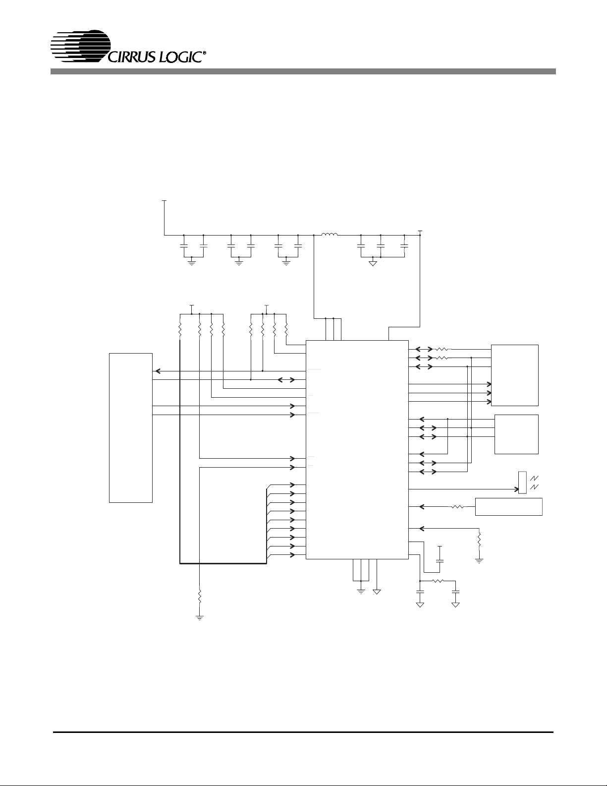
Six typical connection diagrams have been
presented to illustrate using the part with the
different communication modes available. They
are as follows:
Figure 13, "I2C® Control" on page 26
Figure 14, "I2C® Control with External Memory"
on page 27
Figure 15, "SPI Control" on page 28
Figure 16, "SPI Control with External Memory" on
page 29
Figure 17, "Intel® Parallel Control Mode" on page
30
Figure 18, "Motorola® Parallel Control Mode" on
page 31
The following should be noted when viewing the
typical connection diagrams:
The pins are grouped functionally in each of the
typical connection diagrams. Please be aware that
the CS493XX symbol may appear differently in
each diagram.
of integration, many of these pins are internally
multiplexed to serve multiple purposes. Some pins
are designed to operate in one mode at power up,
and serve a different purpose when the DSP is
running. Other pins have functionality which can
be controlled by the application running on the
DSP. In order to better explain the behavior of the
part, the pins which are multiplexed have been
given multiple names. Each name is specific to the
pin’s operation in a particular mode.
An example of this would be the use of pin 20 in
one of the serial control modes. During the boot
period of the CS493XX, pin 20 is called ABOOT.
ABOOT is sampled on the rising edge of RESET.
If ABOOT is high the host must download code to
the DSP. If ABOOT is low when sampled, the
CS493XX goes into autoboot mode and loads itself
with code by generating addresses and reading data
on EMAD[7:0]. When the part has been loaded
with code and is running an application, however,
pin 20 is called INTREQ. INTREQ is an open drain
output used to inform the host that the DSP has an
outgoing message which should be read.
The external memory interface is only supported
when a serial communication mode has been
chosen.
The typical connection diagrams demonstrate the
PLL being used (CLKSEL is pulled low). To use
CLKIN as the DSP clock, CLKSEL should be
pulled high. The system designer must be aware
that certain software features may not be available
if external CLKIN is used as the DSP must run
slower when external CLKIN is used. The system
designer should also be aware of additional duty
cycle requirements when using external CLKIN as
a DSP clock. It is highly suggested that the system
designer use the PLL and pull CLKSEL low.
3.1. Multiplexed Pins
The CS493XX family of digital signal processors
(DSPs) incorporate a large amount of flexibility
into a 44 pin package. Because of the high degree
In this document, pins will be referred to by their
functionality. Section 12, “Pin Descriptions” on
page 80 describes each pin of the CS493XX and
lists all of its names. Please refer to this section
when exact pin numbers are in question.
The part has 12 general purpose input and output
(GPIO[11:0]) pins that all have multiple
functionality. While in one of the parallel
communication modes (Section 6.2, “Parallel Host
Communication” on page 41), these pins are used
to implement the parallel host communication
interface. While in one of the serial host modes
these pins are used to implement an external
memory interface. Alternatively while in one of the
serial host modes these pins could be used for
another general purpose if the application code has
been programmed to support the special purpose.
In this document the pins are referenced by the
24 DS339PP4
CS49300 Family DSP
name corresponding to their particular use.
Sometimes GPIO[11:0], or some subset thereof, is
used when referring to the pins in a general sense.
3.2. Termination Requirements
The CS493XX incorporates open drain pins which
must be pulled high for proper operation. INTREQ
(pin 20) is always an open drain pin which requires
a pull-up for proper operation. When in the I2C
serial communication mode, the SCDIO signal (pin
19) is open drain and thus requires a pull-up for
proper operation.
Due to the internal, multiplexed design of the pins,
certain signals may or may not require termination
depending on the mode being used. If a parallel
host communication mode is not being used,
GPIO[11:0] must be terminated or driven as these
pins will come up as high impedance inputs and
will be prone to oscillation if they are left floating.
The specific termination requirements may vary
since the state of some of the GPIO pins will
determine the communication mode at the rising
edge of reset (please see Section 6, “Control” on
page 32 for more information). For the explicit
termination requirements of each communication
mode please see the typical connection diagrams.
Generally a 4.7k Ohm resistor is recommended for
open drain pins. The communication mode setting
pins (please see Section 6, “Control” on page 32 for
more information) should also be terminated with a
4.7k resistor. A 10k Ohm resistor is sufficient for
the GPIO pins and unused inputs.
3.3. Phase Locked Loop Filter
The internal phase locked loop (PLL) of the
CS493XX requires an external filter for successful
operation. The topology of this filter is shown in
the typical connection diagrams. The component
values are shown below. Care should be taken
when laying out the filter circuitry to minimize
trace lengths and to avoid any close routing of high
frequency signals. Any noise coupled on to the
filter circuit will be directly coupled into the PLL,
which could affect performance.
Reference Designator Value
C1 2.2uF
C2 220pF
C3 10nF
R1 200k Ohm
Table 1. PLL Filter Component Values
4. POWER
The CS493XX requires a 2.5V digital power
supply for the digital logic within the DSP and a
2.5V analog power supply for the internal PLL.
There are three digital power pins, VD1, VD2 and
VD3, along with three digital grounds, DGND1,
DGND2 and DGND3. There is one analog power
pin, VA and one analog ground, AGND. The DSP
will perform at its best when noise has been
eliminated from the power supply. The
recommendations given below for decoupling and
power conditioning of the CS493XX will help to
ensure reliable performance.
4.1. Decoupling
It is good practice to decouple noise from the
power supply by placing capacitors directly
between the power and ground of the CS493XX.
Each pair of power pins (VD1/DGND,
VD2/DGND, VD3/DGND, VA/AGND) should
have its own decoupling capacitors. The
recommended procedure is to place both a 0.1uF
and a 1uF capacitor as close as physically possible
to each power pin. The 0.1uF capacitor should be
closest to the part (typically 5mm or closer).
4.2. Analog Power Conditioning
In order to obtain the best performance from the
CS493XX’s internal PLL, the analog power supply
(VA) must be as clean as possible. A ferrite bead
should be used to filter the 2.5V power supply for
the analog portion of the CS493XX. This power
DS339PP4 25
+2.5 Supply (+2.5VD)
1 uF 0.1 uF
+
Resistor Pack 10k
I2C INTERFACE
MICROCONTROLLER
CS49300 Family DSP
NOTE: A capacitor pair (1 uF and 0.1 uF) must be supplied for each power pin.
NOTE: +2.5VA is simply +2.5VD after filtering through the ferrite bead. Pin 32 must be referenced to +2.5VA
0.1 uF
3.3k
10k
10k
EMAD_GPIO [8:0]
1 uF 0.1 uF
+
1 uF
+
+2.5VD+2.5VD
3.3k
4.7k
4.7k
3.3k
37
DD
38
DC
20
INTREQ
19
SCDIO
6
SCDIN
18
CS
7
SCCLK
36
RESET
4
WR__GPIO10
5
RD__GPIO11
21
GPIO8
8
GPIO7
9
GPIO6
10
GPIO5
11
GPIO4
14
GPIO3
15
GPIO2
16
GPIO1
17
GPIO0
FERRITE BEAD
1
12
23
VD1
VD2
VD3
CS493XX
1 uF 0.1 uF
+
DGND1
DGND2
2
13
DGND3
24
AGND
35
+
34
VA
MCLK
SCLK
LRCLK
AUDATA0
AUDATA1
AUDATA2
CMPDAT
CMPCLK
CMPREQ
SDATAN
SCLKN
SLRCLKN
XMT958
CLKIN
CLKSEL
FLT2
FLT1
+2.5VA
47 uF
44
43
42
41
40
39
27
28
29
22
25
26
3
30
31
32
+2.5VA
33
33
33
DAC (S)
DIR or
ADC [S]
OPT_TX
33
OSCILLATOR
10k
C1
+
R1
3.3k
C2
C3
Figure 13. I2C® Control
26 DS339PP4

CS49300 Family DSP
EXTERNAL
ROM
/CE
/OE
A[15:8]
A[7:0]
D[7:0]
SYSTEM
MICRO
CONTROLLER
Q[7:0]
D[7:0]
+2.5V Supply (+2.5VD)
NOTE: A capacitor pair (1 uF and 0.1 uF) must be supplied for each power pin.
NOTE: +2.5VA is simply +2.5VD after filtering through the ferrite bead. Pin 32 must be referenced to +2.5VA
1 uF 0.1 uF
+
Resistor Pack 10k
I2C INTERFACE
OCTAL F/FOCTAL F/F
Q[7:0]
D[7:0]
1 uF 0.1 uF
+
FERRITE BEAD
0.1 uF
1 uF
+
1 uF
+
0.1 uF
+2.5VA
47 uF
+
+2.5VD+2.5VD
10k
3.3k
EMAD[7:0]
3.3k
10k
3.3k
10k
3.3k
4.7k
4.7k
37
DD
38
DC
20
INTREQ__ABOOT
19
SCDIO
6
SCDIN
18
CS
7
SCCLK
36
RESET
4
WR__GPIO10
5
RD__EMOE
21
EXTMEM
8
EMAD7
9
EMAD6
10
EMAD5
11
EMAD4
14
EMAD3
15
EMAD2
16
EMAD1
17
EMAD0
1
12
23
VD1
VD2
VD3
CS493XX
DGND1
2
DGND2
13
DGND3
24
35
AGND
34
VA
MCLK
SCLK
LRCLK
AUDATA0
AUDATA1
AUDATA2
CMPDAT
CMPCLK
CMPREQ
SDATAN
SCLKN
SLRCLKN
XMT958
CLKIN
CLKSEL
FLT2
FLT1
C2
44
43
42
41
40
39
27
28
29
22
25
26
3
30
31
32
33
33
33
+2.5VA
C1
+
R1
33
OSCILLATOR
10k
C3
DACs
DIR or
ADCs
OPT_TX
Figure 14. I2C® Control with External Memory
DS339PP4 27

+2.5V Supply (+2.5VD)
NOTE: A capacitor pair (1 uF and 0.1 uF) must be supplied for each power pin.
NOTE: +2.5VA is simply +2.5VD after filtering through the ferrite bead. Pin 32 must be referenced to +2.5VA
1 uF 0.1 uF
+
1 uF 0.1 uF
+
CS49300 Family DSP
0.1 uF
+2.5VA
47 uF
+
FERRITE BEAD
0.1 uF
1 uF
+
1 uF
+
SPI INTERFACE
MICROCONTROLLER
+2.5VD
Resistor Pack 10k
3.3k
3.3k
3.3k
EMAD_GPIO [8:0]
+2.5VD
3.3k
4.7k
4.7k
37
DD
38
DC
20
INTREQ
19
SCDOUT
6
SCDIN
18
CS
7
SCCLK
36
RESET
5
RD__GPIO11
4
WR__GPIO10
21
GPIO8
8
GPIO7
9
GPIO6
10
GPIO5
11
GPIO4
14
GPIO3
15
GPIO2
16
GPIO1
17
GPIO0
1
12
23
VD1
VD2
VD3
CS493XX
DGND1
2
DGND2
13
DGND3
24
AGND
35
34
VA
MCLK
SCLK
LRCLK
AUDATA0
AUDATA1
AUDATA2
CMPDAT
CMPCLK
CMPREQ
SDATAN
SCLKN
SLRCLKN
XMT958
CLKIN
CLKSEL
FLT2
FLT1
33
44
33
43
42
41
40
39
27
28
29
22
25
26
3
30
31
32
33
C2
33
+2.5VA
C1
+
R1
C3
DACs
DIR or
ADCs
OPT_TX
OSCILLATOR
10k
Figure 15. SPI Control
28 DS339PP4

CS49300 Family DSP
EXTERNAL
ROM
/CE
/OE
A[15:8]
A[7:0]
D[7:0]
SYSTEM
MICRO
CONTROLLER
Q[7:0]
D[7:0]
+2.5V Supply (+2.5VD)
NOTE: A capacitor pair (1 uF and 0.1 uF) must be supplied for each power pin.
NOTE: +2.5VA is simply +2.5VD after filtering through the ferrite bead. Pin 32 must be referenced to +2.5VA
1 uF 0.1 uF
+
Resistor Pack 10k
SPI INTERFACE
OCTAL F/FOCTAL F/F
Q[7:0]
D[7:0]
1 uF 0.1 uF
+
FERRITE BEAD
0.1 uF
1 uF
+
1 uF
+
0.1 uF
+2.5VA
47 uF
+
+2.5VD+2.5VD
10k
3.3k
3.3k
3.3k
EMAD[7:0]
3.3k
4.7k
4.7k
37
DD
38
DC
20
INTREQ__ABOOT
19
SCDOUT
6
SCDIN
18
CS
7
SCCLK
36
RESET
5
RD__EMOE
4
WR__GPIO10
21
EXTMEM
8
EMAD7
9
EMAD6
10
EMAD5
11
EMAD4
14
EMAD3
15
EMAD2
16
EMAD1
17
EMAD0
1
12
23
VD1
VD2
VD3
CS493XX
DGND1
2
DGND2
13
DGND3
24
35
AGND
34
VA
MCLK
SCLK
LRCLK
AUDATA0
AUDATA1
AUDATA2
CMPDAT
CMPCLK
CMPREQ
SDATAN
SCLKN
SLRCLKN
XMT958
CLKIN
CLKSEL
FLT2
FLT1
C2
44
43
42
41
40
39
27
28
29
22
25
26
3
30
31
32
33
33
33
+2.5VA
C1
+
R1
33
OSCILLATOR
10k
C3
DACs
DIR or
ADCs
OPT_TX
Figure 16. SPI Control with External Memory
DS339PP4 29

+2.5V Supply (+2.5VD)
NOTE: A capacitor pair (1 uF and 0.1 uF) must be supplied for each power pin.
NOTE: +2.5VA is simply +2.5VD after filtering through the ferrite bead. Pin 32 must be referenced to +2.5VA
1 uF 0.1 uF
+
1 uF 0.1 uF
+
FERRITE BEAD
0.1 uF
1 uF 0.1 uF
+
1 uF
+
CS49300 Family DSP
+2.5VA
47 uF
+
INT INTERFACE
MICROCONTROLLER
+2.5VD
3.3k
3.3k
10k
Resistor Pack 10k
DATA[7:0]
+2.5VD
4.7k
3.3k
3.3k
4.7k
37
DD
38
DC
20
INTREQ
8
DATA7
9
DATA6
10
DATA5
11
DATA4
14
DATA3
15
DATA2
16
DATA1
17
DATA0
21 22
GPIO8 SDATAN
5
RD
4
WR
6
A1
7
A0
18
CS
36
RESET
19
PSEL_GPIO9
1
12
23
VD1
VD2
VD3
CS493XX
DGND1
2
DGND2
13
DGND3
24
35
AGND
34
VA
MCLK
SCLK
LRCLK
AUDATA0
AUDATA1
AUDATA2
CMPDAT
CMPCLK
CMPREQ
SCLKN
SLRCLKN
XMT958
CLKIN
CLKSEL
FLT2
FLT1
44
43
42
41
40
39
27
28
29
25
26
3
30
31
32
33
33
33
+2.5VA
C1
+
R1
DACs
DIR or
ADCs
OPT_TX
33
OSCILLATOR
10k
C3C2
Figure 17. Intel® Parallel Control Mode
30 DS339PP4

+2.5V Supply (+2.5VD)
NOTE: A capacitor pair (1 uF and 0.1 uF) must be supplied for each power pin.
NOTE: +2.5VA is simply +2.5VD after filtering through the ferrite bead. Pin 32 must be referenced to +2.5VA
1 uF 0.1 uF
+
1 uF 0.1 uF
+
FERRITE BEAD
0.1 uF
1 uF 0.1 uF
+
1 uF
+
CS49300 Family DSP
+2.5VA
47 uF
+
MOT INTERFACE
MICROCONTROLLER
3.3k
+2.5VD
3.3k
3.3k
10k
Resistor Pack 10k
DATA[7:0]
+2.5VD
3.3k
4.7k
4.7k
37
DD
38
DC
20
INTREQ
8
DATA7
9
DATA6
10
DATA5
11
DATA4
14
DATA3
15
DATA2
16
DATA1
17
DATA0
21 22
GPIO8 SDATAN
19
PSEL_GPIO9
5
R/W__RD
6
A1
7
A0
18
CS
36
RESET
1
12
23
VD1
VD2
VD3
CS493XX
DGND1
2
DGND2
13
DGND3
24
35
AGND
34
VA
MCLK
SCLK
LRCLK
AUDATA0
AUDATA1
AUDATA2
CMPDAT
CMPCLK
CMPREQ
SCLKN
SLRCLKN
XMT958DS__WR
CLKIN
CLKSEL
FLT2
FLT1
44
43
42
41
40
39
27
28
29
25
26
34
30
31
32
33
C2
33
33
+2.5VA
C1
+
R1
DACs
DIR or
ADCs
OPT_TX
33
OSCILLATOR
10k
C3
Figure 18. Motorola® Parallel Control Mode
DS339PP4 31

CS49300 Family DSP
scheme is shown in the typical connection
diagrams.
4.3. Ground
For two layer applications, care should be taken to
have sufficient ground between the DSP and parts
in which it will be interfacing (DACs, ADCs, DIR,
microcontrollers, external memory etc). If there is
not sufficient ground, a potential will be seen
between the ground reference of the DSP and the
interface parts and the noise margin will be
significantly reduced potentially causing
communication or data integrity problems.
4.4. Pads
The CS493XX incorporate 3.3V tolerant pads. This
means that while the CS493XX power supplies
require 2.5 volts, 3.3 volt signals can be applied to
the inputs without damaging the part.
5. CLOCKING
The CS493XX clock manager incorporates a
programmable phase locked loop (PLL) clock
synthesizer. The PLL takes an input reference
clock and produces all the internal clocks required
to run the internal DSP and to provide master mode
timing to the audio input/output peripherals. The
clock manager also includes a 33-bit system time
clock (STC) to support audio and video
synchronization.
The PLL can be internally bypassed by connecting
the CLKSEL pin to VD. This connection
multiplexes the CLKIN pin directly to the DSP
clock. Care should be taken to note the minimum
CLKIN requirements when bypassing the PLL.
The PLL reference clock has three possible sources
that are routed through a multiplexer controlled by
the DSP: SCLKN2, SCLKN1, and CLKIN.
Typically, in audio/video environments like set-top
boxes, the CLKIN pin is connected to 27 MHz. In
other scenarios such as an A/V receiver design, the
PLL can be clocked through the CLKIN pin with
even multiples of the desired sampling rate or with
an already available clock source. Typically a
12.288 MHz CLKIN is used in this scenario so that
the same oscillator can be used for the DSP and
ADC.
The clock manager is controlled by the DSP
application software. The software user’s guide for
the application code being used should be
referenced for what CLKIN input frequency is
supported.
6. CONTROL
Control of the CS493XX can be accomplished
through one of four methods. The CS493XX
supports I2C® and SPI serial communication. In
addition the CS493XX supports both a Motorola
and Intel byte wide parallel host control mode.
Only one of the four communication modes can be
selected for control. The states of the RD, WR, and
PSEL pins are sampled at the rising edge of RESET
to determine the interface type as shown in Table 2.
RD
(Pin 5)WR(Pin 4)
11 1
11 0
01 X
1 0 X Serial SPI
PSEL
(Pin 19)
Table 2. Host Modes
Whichever host communication mode is used, host
control of the CS493XX is handled through the
application software running on the DSP.
Configuration and control of the CS493XX
decoder and its peripherals are indirectly executed
through a messaging protocol supported by the
downloaded application code. In other words
successful communication can only be
accomplished by following the low level hardware
communication format and high level messaging
protocol. The specifications of the messaging
protocol can be found in any of the software user’s
guides.
Host Interface Mode
8-bit Motorola
8-bit Intel
Serial I
®
®
2C®
32 DS339PP4

CS49300 Family DSP
Only the subsection describing the communication
mode being used needs to be read by the system
designer.
6.1. Serial Communication
The CS493XX has a serial control port that
supports both SPI and I2C® forms of
communication.
The following sections will explain each
communication mode in more detail. Flow
diagrams will illustrate read and write cycles.
Timing diagrams will be shown to demonstrate
relative edge positions of signal transitions for read
and write operations.
6.1.1. SPI Communication
SPI communication with the CS493XX is
accomplished with 5 communication lines: chip
select, serial control clock, serial data in, serial data
out and an interrupt request line to signal that the
DSP has data to transmit to the host. Table 3 shows
the mnemonic, pin name, and pin number of each
of these signals on the CS493XX.
Mnemonic Pin Name Pin Number
Chip Select CS
Serial Clock SCCLK 7
Serial Data In SCDIN 6
Serial Data Out SCDOUT 19
Interrupt Request INTREQ
Table 3. SPI Communication Signals
18
20
6.1.1.1.Writing in SPI
When writing to the device in SPI the same
protocol will be used whether writing a byte, a
message or even an entire executable download
image. The examples shown in this document can
be expanded to fit any write situation. Figure 19,
"SPI Write Flow Diagram" on page 33 shows a
typical write sequence:
The following is a detailed description of an SPI
write sequence with the CS493XX.
SPI START: CS (LOW)
WRITE ADDRESS BYTE
WITH MODE BIT
SET TO 0 FOR WRITE
SEND DATABYTE
MORE DATA?
N
(HIGH)
CS
Figure 19. SPI Write Flow Diagram
Y
1) An SPI transfer is initiated when chip select
(CS) is driven low.
2) This is followed by a 7-bit address and the
read/write bit set low for a write. The address
for the CS493XX defaults to 0000000b. It is
necessary to clock this address in prior to any
transfer in order for the CS493XX to accept the
write. In other words a byte of 0x00 should be
clocked into the device preceding any write.
The 0x00 byte represents the 7 bit address
0000000b, and the least significant bit set to 0
to designate a write.
3) The host should then clock data into the device
most significant bit first, one byte at a time. The
data byte is transferred to the DSP on the falling
edge of the eighth serial clock. For this reason,
the serial clock should be default low so that
eight transitions from low to high to low will
occur for each byte.
4) When all of the bytes have been transferred,
chip select should be raised to signify an end of
DS339PP4 33

write. Once again it is crucial that the serial
clock transitions from high to low on the last bit
of the last byte before chip select is raised, or a
loss of data will occur.
The same write routine could be used to send a
single byte, message or an entire application code
image. From a hardware perspective, it makes no
difference whether communication is by byte or
multiple bytes of any length as long as the correct
hardware protocol is followed.
6.1.1.2.Reading in SPI
A read operation is necessary when the CS493XX
signals that it has data to be read. The CS493XX
does this by dropping its interrupt request line
(INTREQ) low. When reading from the device in
SPI, the same protocol will be used whether
reading a single byte or multiple bytes. The
examples shown in this document can be expanded
to fit any read situation. Figure 20, "SPI Read Flow
Diagram" on page 34 shows a typical read
sequence:
CS49300 Family DSP
NO
INTREQ
WRITE ADDRESS BYTE
WITH MODE BIT
SET TO 1 FOR READ
READ DATA BYTE
INTREQ
LOW?
YES
CS (LOW)
YES
STILL LOW?
NO
The following is a detailed description of an SPI
read sequence with the CS493XX.
1) An SPI read transaction is initiated by the
CS493XX dropping INTREQ, signaling that it
has data to be read.
2) The host responds by driving chip select (CS)
low.
3) This is followed by a 7-bit address and the
read/write bit set high for a read. The address
for the CS493XX defaults to 0000000b. It is
necessary to clock this address in prior to any
transfer in order for the CS493XX to
acknowledge the read. In other words a byte of
0x01 should be clocked into the device
preceding any read. The 0x01 byte represents
the 7 bit address 0000000b, and the least
significant bit set to 1 to designate a read.
4) After the falling edge of the serial control clock
CS (HIGH)
Figure 20. SPI Read Flow Diagram
(SCCLK) for the read/write bit, the data is
ready to be clocked out on the control data out
pin (CDOUT). Data clocked out by the host is
valid on the rising edge of SCCLK and data
transitions occur on the falling edge of SCCLK.
The serial clock should be default low so that
eight transitions from low to high to low will
occur for each byte.
5) If INTREQ is still low, another byte should be
clocked out of the CS493XX. Please see the
discussion below for a complete description of
INTREQ behavior.
6) When INTREQ has risen, the chip select line of
the CS493XX should be raised to end the read
34 DS339PP4

CS49300 Family DSP
transaction.
Understanding the role of INTREQ is important for
successful communication. INTREQ is guaranteed
to remain low (once it has gone low) until the
second to last rising edge of SCCLK of the last byte
to be transferred out of the CS493XX. If there is no
more data to be transferred, INTREQ will go high
at this point. For SPI this is the rising edge for the
second to last bit of the last byte to be transferred.
After going high, INTREQ is guaranteed to stay
high until the next rising edge of SCCLK. This end
of transfer condition signals the host to end the read
transaction by clocking the last data bit out and
raising CS. If INTREQ is still low after the second
to last rising edge of SCCLK, the host should
continue reading data from the serial control port.
It should be noted that all data should be read out of
the serial control port during one cycle or a loss of
data will occur. In other words, all data should be
read out of the chip until INTREQ signals the last
byte by going high as described above. Please see
Section 6.1.3, “INTREQ Behavior: A Special
Case” on page 39 for a more detailed description of
INTREQ behavior.
Figure 21, "SPI Timing" on page 36 timing
diagram shows the relative edges of the control
lines for an SPI read and write.
page 35 shows the mnemonic, pin name, and pin
number of each of these signals on the CS493XX.
Mnemonic Pin Name Pin Number
Serial Clock SCCLK 7
Bi-Directional Data SCDIO 19
Interrupt Request INTREQ
2
Tab l e 4. I
C® Communication Signals
20
Typically in I2C® communication SCDIO is an
open drain line with a pull-up. A logic one is placed
on the line by three-stating the output and allowing
the pull-up to raise the line. At this point another
device can drive the line low if necessary. Threestating SCDIO can have two effects: 1. To send out
a one when writing data or sending a “no
acknowledge”; 2. release the line when another
chip is writing data.
6.1.2.1.Writing in I2C
®
When writing to the device in I2C® the same
protocol will be used whether writing a byte, a
message or even an application code image. The
examples shown in this document can be expanded
to fit any write situation. Figure 23 shows a typical
write sequence:
The following is a detailed description of an I2C
write sequence with the CS493XX.
®
6.1.2. I2C Communication
I2C communication with the CS493XX is
accomplished with 3 communication lines: serial
control clock, a bi-directional serial data
input/output line and an interrupt request line to
signal that the DSP has data to transmit to the host.
See Figure 4, "I2C® Communication Signals" on
condition which is defined as the data (SCDIO)
line falling while the clock (SCCLK) is held
high.
2) Next a 7-bit address with the read/write bit set
low for a write should be sent to the CS493XX.
The address for the CS493XX defaults to
0000000b. It is necessary to clock this address
in prior to any transfer in order for the
CS493XX to accept the write. In other words a
byte of 0x00 should be clocked into the device
preceding any write. The 0x00 byte represents
the 7 bit of address (0000000b) and the
read/write bit set to 0 to designate a write.
DS339PP4 35
1) An I2C® transfer is initiated with an I2C® start

CS49300 Family DSP
Note 2
Note 1
going LOW at this
SP I W rite Functional Tim ing
D7 D6 D5 D4 D3 D2 D1 D0 D7 D6 D5 D4 D3 D2 D1 D0 D7 D6 D5 D4 D3 D2 D1 D0
R/W
AD0
SPI Read Functional Tim ing
is guaranteed to stay LOW until the rising edge of SCCLK for bit D1 of the last byte
is guaranteed to remain HIGH until the next rising edge of SCCLK at which point it
point should be treated as a new read condition. After a stop condition, a new start condition
to be transferred out of the CS493XX.
and an address byte should be sent
may go LOW again if there is new data to be read. The condition of INTREQ
2. INTREQ
Notes: 1. INTREQ
Figure 21. SPI Timing
AD6 AD4AD5 AD3 AD2 AD1 AD0 R/W D7 D6 D5 D4 D3 D2 D1 D0 D7 D6 D5 D4 D3 D2 D1 D0 D7 D6 D5 D4 D3 D2 D1 D0
CS
SCDIN
SCCLK
AD6 AD4AD 5 AD3 AD2 AD1
CS
SCDIN
SCCLK
SCDOUT
INTR EQ
36 DS339PP4

CS49300 Family DSP
3) After each byte (including the address and each
data byte) the host must release the data line
and provide a ninth clock for the CS493XX to
acknowledge. The CS493XX will drive the
data line low during the ninth clock to
acknowledge. If for some reason the CS493XX
does not acknowledge, it means that the last
byte sent was not received and should be resent.
If the resent byte fails to produce an
acknowledge, a stop condition should be sent
and the device should be reset.
4) The host should then clock data into the device
most significant bit first, one byte at a time. The
SEND I2C START:
DROP SCDIO LOW
WHILE SCCLK IS HIGH
CS493XX will (and must) acknowledge each
byte that it receives which means that after each
byte the host must provide an acknowledge
clock pulse on SCCLK and release the data
line, SCDIO.
5) At the end of a data transfer a stop condition
must be sent. The stop condition is defined as
the rising edge of SCDIO while SCCLK is
high.
6.1.2.2.Reading in I2C
®
A read operation is necessary when the CS493XX
signals that it has data to be read. It does this by
dropping its interrupt request line (INTREQ) low.
When reading from the device in I2C®, the same
protocol will be used whether reading a single byte
or multiple bytes. The examples shown in this
document can be expanded to fit any read situation.
Figure 23 shows a typical I2C® read sequence
WRITE ADDRESS BYTE
WITH MODE BIT
SET TO 0 FOR WRITE
GET ACK
SEND DATABYTE
GET ACK
MORE DATA?
N
2
C STOP:
I
RAISE SCDIO HIGH
WHILE SCCLK IS HIGH
Figure 22. I2C® Write Flow Diagram
Y
1) An I2C® read transaction is initiated by the
CS493XX dropping INTREQ, signaling that it
has data to be read.
2) The host responds by sending an I2C® start
condition which is SCDIO dropping while
SCCLK is held high.
3) The start condition is followed by a 7-bit
address and the read/write bit set high for a
read. The address for the CS493XX defaults to
0000000b. It is necessary to clock this address
in prior to any transfer in order for the
CS493XX to acknowledge the read. In other
words a byte of 0x01 should be clocked into the
device preceding any read. The 0x01 byte
represents the 7 bit address 0000000b and a
read/write bit set to 1 to designate a read.
4) After the falling edge of the serial control clock
(SCCLK) for the read/write bit of the address
byte, an acknowledge must be read in by the
host. The CS493XX will drive SCDIO low to
acknowledge the address byte and to indicate
that it is ready for a read operation. If an
DS339PP4 37

CS49300 Family DSP
acknowledge is not sent by the CS493XX, a
stop condition should be issued and the read
sequence should be restarted.
5) The data is ready to be clocked out on the
SCDIO line at this point. Data clocked out by
the host is valid on the rising edge of SCCLK
and data transitions occur on the falling edge of
SCCLK.
INTREQ
SEND I2C START:
DROP SCDIO LOW
WHILE SCCLK IS HIGH
WRITE ADDRESS BYTE
WITH MODE BIT
SET TO 1 FOR READ
READ DATABYTE
INTREQ
LOW?
YES
GET ACK
STILL LOW?
NO
YES
SEND ACK
6) If INTREQ is still low after a byte transfer, an
acknowledge (SCDIO clocked low by SCCLK)
must be sent by the host to the CS493XX and
another byte should be clocked out of the
CS493XX. Please see the discussion below for
a complete description of INTREQ’s behavior.
7) When INTREQ has risen, a no acknowledge
should be sent by the host (SCDIO clocked
high by the host) to the CS493XX. This,
followed by an I2C® stop condition (SCDIO
raised, while SCCLK is high) signals an end of
read to the CS493XX.
Understanding the role of INTREQ is important for
successful communication. INTREQ is guaranteed
to remain low (once it has gone low), until the
rising edge of SCCLK for the last bit of the last byte
to be transferred out of the CS493XX (i.e. the
rising edge of SCCLK before the ACK SCCLK). If
there is no more data to be transferred, INTREQ
will go high at this point. After going high,
INTREQ is guaranteed to stay high until the next
rising edge of SCCLK (i.e. it will stay high until the
rising edge of SCCLK for the ACK/NACK bit).
This end of transfer condition signals the host to
end the read transaction by clocking the last data bit
out of the CS493XX and then sending a no
acknowledge to the CS493XX to signal that the
read sequence is over. At this point the host should
send an I2C® stop condition to complete the read
sequence. If INTREQ is still low after the rising
edge of SCCLK on the last data bit of the current
byte, the host should send an acknowledge and
continue reading data from the serial control port.
NO
It should be noted that all data should be read out of
the serial control port during one cycle or a loss of
SEND NACK
data will occur. In other words, all data should be
read out of the chip until INTREQ signals the last
SEND I2C STOP:
RISING EDGE OF SCDIO
WHILE SCLK IS HIGH
Figure 23. I2C® Read Flow Diagram
38 DS339PP4
byte by going high as described above. Please see
Section 6.1.3, “INTREQ Behavior: A Special
Case” on page 39 for a more detailed description of
INTREQ behavior.

CS49300 Family DSP
The timing diagram in Figure 24, "I2C® Timing"
on page 40 shows the relative edges of the control
lines for an I2C® read and write.
6.1.3. INTREQ Behavior: A Special Case
When communicating with the CS493XX there are
two types of messages which force INTREQ to go
low. These messages are known as solicited
messages and unsolicited messages. For more
information on the specific types of messages that
require a read from the host, one of the application
code user’s guides should be referenced.
In general, when communicating with the
CS493XX, INTREQ will not go low unless the
host first sends a read request command message.
In other words the host must solicit a response from
the DSP. In this environment, the host must read
from the CS493XX until INTREQ goes high again.
Once the INTREQ pin has gone high it will not be
driven low until the host sends another read
request.
When unsolicited messages, such as those used for
Autodetect, have been enabled, the behavior of
INTREQ is noticeably different. The CS493XX
will drop the INTREQ pin whenever the DSP has
an outgoing message, even though the host may not
have requested data.
There are three ways in which INTREQ can be
affected by an unsolicited message:
1) During normal operation, while INTREQ is
high, the DSP could drop INTREQ to indicate an
outgoing message, without a prior read request.
2) The host is in the process of reading from the
CS493XX, meaning that INTREQ is already low.
An unsolicited message arrives which forces
INTREQ to remain low after the solicited message
is read.
3) The host is reading from the CS493XX when the
unsolicited message is queued, but INTREQ goes
high for one period of SCCLK and then goes low
again before the end of the read cycle.
In case (1) the host should perform a read operation
as discussed in the previous sections.
In case (2) an unsolicited message arrives before
the second to last SCCLK of the final byte transfer
of a read, forcing the INTREQ pin to remain low.
In this scenario the host should continue to read
from the CS493XX without a stop/start condition
or data will be lost.
In case (3) an unsolicited message arrives between
the second to last SCCLK and the last SCCLK of
the final byte transfer of a read. In this scenario,
INTREQ will transition high for one clock (as if the
read transaction has ended), and then back low
(indicating that more data has queued). This final
case is the most complicated and shall be explained
in detail.
There are two constraints which completely
characterize the behavior of the INTREQ pin
during a read. The first constraint is that the
INTREQ pin is guaranteed to remain low until the
second to last SCCLK (SCCLK number N-1) of the
final byte being transferred from the CS493XX
(not necessarily the second to last bit of the data
byte). The second constraint is that once the
INTREQ pin has gone high it is guaranteed to
remain high until the rising edge of the last SCCLK
(SCCLK number N) of the final byte being
transferred from the CS493XX (not necessarily the
last bit of the data byte). If an unsolicited message
arrives in the window of time between the rising
edge of the second to last SCCLK and the final
SCCLK, INTREQ will drop low on the rising edge
of the final SCCLK as illustrated in the functional
timing diagrams shown for I2C® and SPI read
cycles.
INTREQ behavior for I2C® communication is
illustrated in Figure 24, "I2C® Timing" on page
40. When using I2C® communication the INTREQ
pin will remain low until the rising edge of SCCLK
DS339PP4 39

CS49300 Family DSP
CStop
CStop
2
2
Note 5
Note 4
Note 2
Timing
®
C
2
C Read Functional Tim ing
2
C Write Functional Timing
I
2
I
Note 1 Note 3
to be transferred out of the CS493XX.
2. The ACKs for the data bytes being read from the CS493XX should be driven by the host.
3. INTREQ
is guaranteed to stay LOW until the rising edge of SCCLK for bit D0 of the last byte
4. A NACK should be sent by the host after the last byte to indicate the end of the read cycle.
is guaranteed to stay HIGH until the next rising edge of SCCLK (for the ACK/NACK
5. INTREQ
bit) at which point it may go LOW again if there is new data to be read. The condition of
going LOW at this point should be treated as a new read condition. After a stop
condition, a new start condition followed by an address byte should be sent.
INTREQ
Figure 24. I
Notes: 1. The ACK for the address byte is driven by the CS493XX.
AD6 AD4AD5 AD3 AD2 AD1 AD0 R/W D7 D6 D5 D4 D3 D2 D1 ACKD0ACK D7 D6 D5 D4 D3 D2 D1 ACKD0 D7 D6 D5 D4 D3 D2 D1 ACKD0
CStart I
2
CStart I
2
I
I
AD6 AD4AD5 AD3 A D2 AD1 A D0 R /W D7 D6 D 5 D4 D3 D2 D1 ACKD0ACK D7 D 6 D5 D4 D3 D2 D1 ACKD0 D7 D6 D5 D4 D3 D2 D1 NACKD0
SCDIO
SCCLK
SCDIO
SCCLK
INTREQ
40 DS339PP4

CS49300 Family DSP
for the data bit D0 (SCCLK N-1), but it can go low
at the rising edge of SCCLK for the NACK bit
(SCCLK N) if an unsolicited message has arrived.
If no unsolicited messages arrive, the INTREQ pin
will remain high after rising.
INTREQ behavior for SPI communication is
illustrated in Figure 21, "SPI Timing" on page 36.
When using SPI communication, the INTREQ pin
will remain low until the rising edge of SCCLK for
the data bit D1 (SCCLK N-1), but it can go low at
the rising edge of SCCLK for data bit D0 (SCCLK
N) if an unsolicited message has arrived. If no
unsolicited messages arrive, the INTREQ pin will
remain high after rising.
Ideally, the host will sample INTREQ on the
falling edge of SCCLK number N-1 of the final
byte of each read response message. If INTREQ is
sampled high, the host should conclude the current
read cycle using the stop condition defined for the
communication mode chosen. The host should then
begin a new read cycle complete with the
appropriate start condition and the chip address. If
INTREQ is sampled low, the host should continue
reading the next message from the CS493XX
without ending the current read cycle.
read response message. It is guaranteed that no read
responses will begin with 0x00, which means that a
NULL byte (0x00) detected in the OPCODE
position of a read response message should be
discarded. Please see an Application Code User’s
Guide for an explanation of the OPCODE.
It is important that the host be aware of the
presence of NULL bytes, or the communication
channel could become corrupted.
When case (3) occurs and the host issues a stop
condition before starting a new read cycle, the first
byte of the unsolicited message is loaded directly
into the shift register and 0x00 is never seen.
Alternatively, if case (3) occurs and the host
continues to read from the CS493XX without a
stop condition (a multiple message read), the 0x00
byte must be shifted out of the CS493XX before
the first byte of the unsolicited message can be
read.
In other words, if a system can only sample
INTREQ after an entire byte transfer the following
routine should be used if INTREQ is low after the
last byte of the message being read:
1) Read one byte
When using automated communication ports,
however, the host is often limited to sampling the
status of INTREQ after an entire byte has been
transferred. In this situation a low-high-low
transition (case 3) would be missed and the host
will see a constantly low INTREQ pin. Since the
host should read from the CS493XX until it detects
that INTREQ has gone high, this condition will be
treated as a multiple-message read (more than one
read response is provided by the CS493XX). Under
these conditions a single byte of 0x00 will be read
out before the unsolicited message.
The length of every read response is defined in the
user’s manual for each piece of application code.
Thus, the host should know how many bytes to
expect based on the first byte (the OPCODE) of a
DS339PP4 41
2) If the byte = 0x00 discard it and skip to step 3.
If the byte != 0x00 then it is the OPCODE for
the next message. For this case skip to step 4.
3) Read one more byte. This is the OPCODE for
the next message.
4) Read the rest of the message as indicated in the
previous sections.
6.2. Parallel Host Communication
The parallel host communication modes of the
CS493XX provide an 8-bit interface to the DSP.
An Intel-style parallel mode and a Motorola-style
parallel mode are supported. The host interface is
implemented using four communication registers
within the CS493XX as shown in Table 5, “Parallel
Input/Output Registers,” on page 42.

CS49300 Family DSP
Host Message (HOSTMSG) Register, A[1:0] = 00b
76543210
HOSTMSG7 HOSTMSG6 HOSTMSG5 HOSTMSG4 HOSTMSG3 HOSTMSG2 HOSTMSG1 HOSTMSG0
HOSTMSG7–0 Host data to and from the DSP. A read or write of this register operates handshake bits between
the internal DSP and the external host. This register typically passes multibyte messages carrying microcode, control, and configuration data. HOSTMSG is physically implemented as two
independent registers for input and output (read and write).
Host Control (CONTROL) Register, A[1:0] = 01b
76543210
Reserved CMPRST PCMRST MFC MFB HINBSY HOUTRDY Reserved
Reserved Always write a 0 for future compatibility.
CMPRST When set, initializes the CMPDATA compressed data input channel. Writing a one to this bit
holds the port in reset. Writing zero enables the port. This bit must be low for normal operation.
(Write only)
PCMRST When set, initializes the PCMDATA linear PCM input channel. Writing a one to this bit holds the
port in reset. Writing zero enables the port. This bit must be low for normal operation. (Write
only)
MFC When high, indicates that the PCMDATA input buffer is almost full. (read only)
MFB When high, indicates that the CMPDATA input buffer is almost full. (read only)
HINBSY Set when the host writes to HOSTMSG. Cleared when the DSP reads data from the HOSTMSG
register. The host reads this bit to determine if the last host byte written has been read by the
DSP. (Read only)
HOUTRDY Set when the DSP writes to the HOSTMSG register. Cleared when the host reads data from
the HOSTMSG register. The DSP reads this bit to determine if the last DSP output byte has
been read by the host. (read only)
Reserved Always write a 0 for future compatibility.
PCM Data Input (PCMDATA) Register, A[1:0] = 10b
76543210
PCMDATA7 PCMDATA6 PCMDATA5 PCMDATA4 PCMDATA3 PCMDATA2 PCMDATA1 PCMDATA0
PCMDATA7–0 The host writes PCM data to the DSP input buffer at this address. (Write only)
Compressed Data Input (CMPDATA) Register, A[1:0] = 11b
76543210
CMPDATA7 CMPDATA6 CMPDATA5 CMPDATA4 CMPDATA3 CMPDATA2 CMPDATA1 CMPDATA0
CMPDATA7–0 The host writes compressed data to the DSP input buffer at this address. (Write only)
Table 5. Parallel Input/Output Registers
42 DS339PP4

CS49300 Family DSP
When the host is downloading code to the
CS493XX or configuring the application code,
control messages will be written to (and read from)
the Host Message register. The Host Control
register is used during messaging sessions to
determine when the CS493XX can accept another
byte of control data, and when the CS493XX has an
outgoing byte that may be read.
The PCM Data and Compressed Data registers are
used strictly for the transfer of audio data. The host
cannot read from these two registers. Audio data
written to registers 11b and 10b are transferred
directly to the internal FIFOs of the CS493XX.
When the level of the PCM FIFO reaches the FIFO
threshold level, the MFC bit of the Host Control
register will be set. When the level of the
Compressed Data FIFO reaches the FIFO threshold
level, the MFB bit of the Host Control register will
be set.
It is important to remember that the parallel host
interface requires the DATA[7:0] pins of the
CS493XX. The external memory interface also
requires the DATA[7:0] pins so the Parallel host
control modes can only be used if external memory
is not required.
A detailed description for each parallel host mode
will now be given. The following information will
be provided for the Intel mode and Motorola mode:
• The pins of the CS493XX which must be used
for proper communication
• Flow diagram and description for a parallel
byte write
• Flow diagram and description for a parallel
byte read
The four registers of the CS493XX’s parallel host
mode are not used identically. The algorithm used
for communicating with each register will be given
as a functional description, building upon the basic
read and write protocols defined in the Motorola
and Intel sections. The following will be covered:
• Flow diagram and description for a control
write
• Flow diagram and description for a control read
6.2.1. Intel Parallel Host Communication
Mode
The Intel parallel host communication mode is
implemented using the pins given in Table 6.
The INTREQ pin is controlled by the application
code when a parallel host communication mode has
been selected. When the code supports INTREQ
notification, the INTREQ pin is asserted whenever
the DSP has an outgoing message for the host. This
same information is reflected by the HOUTRDY
bit of the Host Control Register (A[1:0] = 01b).
INTREQ is useful for informing the host of
unsolicited messages. An unsolicited message is
defined as a message generated by the DSP without
an associated host read request. Unsolicited
messages can be used to notify the host of
Mnemonic Pin Name Pin Number
Chip Select CS
Write Enable WR
Output Enable RD
Register Address Bit 1 A1 6
Register Address Bit 0 A0 7
Interrupt Request INTREQ
DATA7 DATA7 8
DATA6 DATA6 9
DATA5 DATA5 10
DATA4 DATA4 11
DATA3 DATA3 14
DATA2 DATA2 15
DATA1 DATA1 16
DATA0 DATA0 17
Table 6. Intel Mode Communication Signals
conditions such as a change in the incoming audio
data type (e.g. PCM --> AC-3).
18
4
5
19
DS339PP4 43

CS49300 Family DSP
6.2.1.1.Writing a Byte in Intel Mode
Information provided in this section is intended as
a functional description of how to write control
information to the CS493XX. The system designer
must insure that all of the timing constraints of the
Intel Parallel Host Mode Write Cycle are met.
The flow diagram shown in Figure 24 illustrates
the sequence of events that define a one-byte write
in Intel mode. The protocol presented in Figure 24
will now be described in detail.
1) The host must first drive the A1 and A0 register
address pins of the CS493XX with the address
of the desired Parallel I/O Register.
Host Message: A[1:0]==00b.
Host Control: A[1:0]==01b.
PCMDATA: A[1:0]==10b.
CMPDATA: A[1:0]==11b.
2) The host then indicates that the selected register
will be written. The host initiates a write cycle
by driving the CS and WR pins low.
3) The host drives the data byte to the DATA[7:0]
pins of the CS493XX.
4) Once the setup time for the write has been met,
ADDRESS A PARALLEL I/O REGISTER
(A[1:0] SET APPROPRIATELY
the host ends the write cycle by driving the CS
and WR pins high.
6.2.1.2.Reading a Byte in Intel Mode
Information provided in this section is intended as
a functional description of how to write control
information to the CS493XX. The system designer
must insure that all of the timing constraints of the
Intel Parallel Host Mode Read Cycle are met.
The flow diagram shown in Figure 25 illustrates
the sequence of events that define a one-byte read
in Intel mode. The protocol presented in Figure 25
will now be described in detail.
1) The host must first drive the A1 and A0 register
address pins of the CS493XX with the address
of the desired Parallel I/O Register. Note that
only the Host Message register and the Host
Control register can be read.
Host Message: A[1:0]==00b.
Host Control: A[1:0]==01b.
2) The host now indicates that the selected register
will be read. The host initiates a read cycle by
driving the CS and RD pins low.
3) Once the data is valid, the host can read the
value of the selected register from the
DATA[7:0] pins of the CS493XX.
ADDRESS A PARALLEL I/O REGISTER
(A[1:0] SET APPROPRIATELY
CS (LOW )
WR (LOW )
WRITE BYTE TO
DATA [7:0]
CS
(HIGH)
WR (HIGH)
Figure 24. Intel Mode, One-Byte Write Flow Diagram
44 DS339PP4
Figure 25. Intel Mode, One-Byte Read Flow Diagram
CS (LOW )
RD (LOW )
READ BYTE FROM
DATA [7:0]
CS (HIGH)
RD (HIGH)

CS49300 Family DSP
4) The host should now terminate the read cycle
by driving the CS and RD pins high.
6.2.2. Motorola Parallel Host
Communication Mode
The Motorola parallel host communication mode is
implemented using the pins given in Table 7. The
INTREQ pin is controlled by the application code
when a parallel host communication mode has been
selected. When the code supports INTREQ
notification, the INTREQ pin is asserted whenever
the DSP has an outgoing message for the host. This
same information is reflected by the HOUTRDY
bit of the Host Control Register (A[1:0] = 01b).
INTREQ is useful for informing the host of
unsolicited messages. An unsolicited message is
defined as a message generated by the DSP without
an associated host read request. Unsolicited
messages can be used to notify the host of
conditions such as a change in the incoming audio
data type (e.g. PCM --> AC-3)
Mnemonic Pin Name Pin Number
Chip Select CS
Data Strobe DS
Read or Write Select R/W
Register Address Bit 1 A1 6
Register Address Bit 0 A0 7
Interrupt Request INTREQ
DATA7 DATA7 8
DATA6 DATA6 9
DATA5 DATA5 10
DATA4 DATA4 11
DATA3 DATA3 14
DATA2 DATA2 15
DATA1 DATA1 16
DATA0 DATA0 17
Table 7. Motorola Mode Communication Signals
18
4
5
19
must insure that all of the timing constraints of the
Motorola Parallel Host Mode Write Cycle are met.
The flow diagram shown in Figure 26 illustrates
the sequence of events that define a one-byte write
in Motorola mode. The protocol presented in
Figure 26 will now be described in detail.
1) The host must drive the A1 and A0 register
address pins of the CS493XX with the address
of the address of the desired Parallel I/O
Register.
Host Message: A[1:0]==00b.
Host Control: A[1:0]==01b.
PCMDATA: A[1:0]==10b.
CMPDATA: A[1:0]==11b.
The host indicates that this is a write cycle by
driving the R/W pin low.
2) The host initiates a write cycle by driving the
CS and DS pins low.
3) The host drives the data byte to the DATA[7:0]
pins of the CS493XX.
4) Once the setup time for the write has been met,
R/W (LOW)
ADDRESS A PARALLEL I/O REGISTER
(A[1:0] SET APPROPRIATELY
CS (LO W)
DS (LOW )
WRITE BYTE TO
DATA [7:0]
6.2.2.1.Writing a Byte in Motorola Mode
CS (HIGH)
(HIGH)
DS
Information provided in this section is intended as
a functional description of how to write control
information to the CS493XX. The system designer
DS339PP4 45
Figure 26. Motorola Mode, One-Byte Write Flow
Diagram

CS49300 Family DSP
the host ends the write cycle by driving the CS
and DS pins high.
6.2.2.2.Reading a Byte in Motorola Mode
The flow diagram shown in Figure 27 illustrates
the sequence of events that define a one-byte read
in Motorola mode. The protocol presented
Figure 27 will now be described in detail.
1) The host must drive the A1 and A0 register
address pins of the CS493XX with the address
of the desired Parallel I/O Register. Note that
only the Host Message register and the Host
Control register can be read.
Host Message: A[1:0]==00b.
Host Control: A[1:0]==01b.
The host indicates that this is a read cycle by
driving the R/W pin high.
2) The host initiates the read cycle by driving the
CS and DS pins low.
3) Once the data is valid, the host can read the
value of the selected register from the
DATA[7:0] pins of the CS493XX.
4) The host should now terminate the read cycle
by driving the CS and DS pins high.
6.2.3. Procedures for Parallel Host Mode
Communication
6.2.3.1.Control Write in a Parallel Host Mode
When writing control data to the CS493XX, the
same protocol is used whether the host is writing a
control message or an entire executable download
image. Messages sent to the CS493XX should be
written most significant byte first. Likewise,
downloads of the application code should also be
performed most significant byte first.
The example shown in this section can be
generalized to fit any control write situation. The
generic function ‘Read_Byte_*()’ is used in the
following example as a generalized reference to
either Read_Byte_MOT() or Read_Byte_INT(),
and ‘Write_Byte_*()’ is a generic reference to
Write_Byte_MOT() or Write_Byte_INT().
Figure 28 shows a typical write sequence. The
protocol presented in Figure 28 will now be
described in detail.
R/W (HIGH)
ADDRESS A PARALLEL I/O REGISTER
(A[1:0] SET APPROPRIATELY
CS (LO W)
DS (LO W)
READ BYTE FROM
DATA [7:0]
CS (HIGH)
DS (HIGH)
Figure 27. Motorola Mode, One-Byte Read Flow
Diagram
1) When the host is communicating with the
CS493XX, the host must verify that the DSP is
ready to accept a new control byte. If the DSP
is in the midst of an interrupt service routine, it
will be unable to retrieve control data from the
Host Message Register. Please note that
‘Read_Byte_*()’ and ‘Write_Byte_*()’ are
generic references to either the Intel or
Motorola communication protocol.
If the most recent control byte has not yet been
read by the DSP, the host must not write a new
byte.
2) In order to determine whether the CS493XX is
ready to accept a new control byte the host must
check the HINBSY bit of the Host Control
Register (bit 2). If HINBSY is high, then the
DSP is not prepared to accept a new control
46 DS339PP4

CS49300 Family DSP
byte, and the host should poll the Host Control
Register again. If HINBSY is low, then the host
may write a control byte into the Host Message
Register.
3) The host knows that the DSP is ready for a new
control byte at this point and should write the
control byte to the Host Message Register
(A[1:0] = 00b).
4) If the host would like to write any more control
bytes to the CS493XX, the host should once
again poll the Host Control Register (return to
step 1).
6.2.3.2.Control Read in a Parallel Host Mode
When reading control data from the CS493XX, the
same protocol is used whether the host is reading a
single byte or a 6 byte message.
During the boot procedure, a handshaking protocol
is used by the CS493XX. This handshake consists
of a 3 byte write to the CS493XX followed by a 1
READ_BYTE_*(HOST CONTROL REGISTER)
byte response from the DSP. The host must read the
response byte and act accordingly. The boot
procedure is discussed in Section 8.1, “Host Boot”
on page 52.
During regular operation (at run-time), the
responses from the CS493XX will always be 6
bytes in length.
The example shown in this section can be used for
any control read situation. The generic function
‘Read_Byte_*()’ is used in the following example
as a generalized reference to either
Read_Byte_MOT() or Read_Byte_INT().
Figure 29 shows a typical read sequence. The
protocol presented in Figure 29 will now be
described in detail.
1) Optionally, INTREQ going low may be used as
an interrupt to the host to indicate that the
CS493XX has an outgoing message. Even with
the use of INTREQ, HOUTRDY must be
checked to insure that bytes are ready for the
host during the read process. Please note that
INTREQ does not go low to indicate an
outgoing message during boot.
YES
HINSBY==1
NO
WRITE_BYTE_*(HOST MESSAGE REGISTER)
YES
Figure 28. Typical Parallel Host Mode Control
Write Sequence Flow Diagram
MORE BYTES
TO WRITE?
NO
FINISHED
2) The host reads the Host Control Register
(A[1:0] = 01b) in order to determine the state of
the communication interface. Please note that
‘Read_Byte_*()’ is a generalized reference to
either Read_Byte_MOT() or
Read_Byte_INT().
3) In order to determine whether the CS493XX
has an outgoing control byte that is valid, the
host must check the HOUTRDY bit of the Host
Control Register (bit 1). If HOUTRDY is high,
then the Host Message Register contains a valid
message byte for the host. If HOUTRDY is
low, then the DSP has not placed a new control
byte in the Host Message Register, and the host
should poll the Host Control Register again.
4) The host knows that the DSP is ready to
provide a new response byte at this point. The
DS339PP4 47

INTREQ = 0
YES
READ_BYTE_*(HOST CONTROL REGISTER)
NO
HOUTRDY==1
YES
READ_BYTE_*(HOST MESSAGE REGISTER)
YES
MORE BYTES
TO READ?
NO
WAIT 100 uS
CS49300 Family DSP
host can safely read a byte from the Host
Message Register (A[1:0] = 00b).
5) If the host expects to read any more response
bytes, the host should once again check the
HOUTRDY bit (return to step 1). Please refer
to one of the application code user’s guides to
determine the length of messages to read from
the CS493XX. Typically this length is 1, 3 or 6
bytes, and can be deduced from the message
OPCODE.
6) After the response has been read the host
should wait at least 100 uS and check
HOUTRDY one final time. If HOUTRDY is
high once again this means that an unsolicited
message has come during the read process and
the host has another message to read (i.e. skip
back to step 4 and read out the new message).
7. EXTERNAL MEMORY
If using one of the serial modes, i.e. SPI or I2C, the
system designer has the option of using external
memory. The external memory interface is not
compatible with the parallel modes since there are
shared pins that are needed by each mode.
READ_BYTE_*(HOST CONTROL REGISTER)
The external memory interface was designed for
autoboot and to extend the data memory range of
the DSP during runtime. The application user’s
YES
HOUTRDY==1
guide for a particular code load will inform the
system designer if memory is required. If no
mention is made of external memory, then external
NO
FINISHED
Figure 29. Typical Parallel Host Mode Control Read
Sequence Flow Diagram
memory is not required for that application.
The external memory interface is implemented on
the CS493XX with the following signals:
EMAD[7:0], EXTMEM, EMOE, and EMWR.
Table 8 shows the pin name, pin description and
pin number of each signal on the CS493XX.
EMAD[7:0] serve as a multiplexed address and
data bus. EMOE is an active-low external-memory
data output enable as well as the address latch
strobe. EMWR is an active low write enable.
48 DS339PP4

CS49300 Family DSP
EXTMEM serves as the active low chip select
output.
Pin
Pin Name Pin Description
/EMOE * External Memory Output Enable
& Address Latch Strobe
/EMWR * External Memory Write Strobe 4
/EXTMEM External Memory Select 21
EMAD7 Address and Data Bit 7 8
EMAD6 Address and Data Bit 6 9
EMAD5 Address and Data Bit 5 10
EMAD4 Address and Data Bit 4 11
EMAD3 Address and Data Bit 3 14
EMAD2 Address and Data Bit 2 15
EMAD1 Address and Data Bit 1 16
EMAD0 Address and Data Bit 0 17
* - These pins must be configured appropriately to select a serial host communication mode for the CS493XX at the rising
edge of RESET
Table 8. Memory Interface Pins
Number
5
Figure 30, "External Memory Interface" on page
51 illustrates one possible external memory
architecture for the CS493XX. Figure 31,
"External Memory Read (16-bit address)" on page
51 shows the functional timing of a 16 bit address
memory read and Figure 32, "External Memory
Write (16-bit address)" on page 51 shows the
functional timing of a 16 bit address memory write.
It should be noted that this memory example gives
the DSP visibility to up to 64 kilobytes of memory.
The external memory address is capable of
addressing up to 16 megabytes total through a 24
bit addressing scheme. The address comes from the
DSP writing three initial bytes of address
consecutively on EMAD[7:0]. Each byte of
address is externally latched with the rising edge of
EMOE while EXTMEM is high. After the 3-byte
address is latched externally, the CS493XX then
drives EXTMEM and EMOE low simultaneously
to select the external memory. During this time the
data is read by the CS493XX.
To extend the example shown in Figures 30 to 32
to allow for a 24-bit address, the system designer
would add another latch to the system. The DSP
always places the most significant address bits first
(see Figures 30, 31, and 32 for details).
It should be noted that there are currently no
applications for the CS493XX that use more than
32 kilobytes of external memory (RAM or ROM),
which corresponds to only 15 address lines.
7.1. Non-Paged Memory
Non-paged memories can be used for autobooting
a single piece of full download application code
such as MP3, HDCD, or SRS Circle Surround. A
non-paged memory architecture should be used in
systems which will need to access a single dsp
application code image (32 Kilobyte maximum),
which means that only 15 bits would be required to
access the entire application code image. The 16th
address bit coming from the DSP should be left
unconnected. Figure 35 shows the functional
timing of an autoboot sequence in which three
address cycles are illustrated.
The DSP always considers its address space to
range from 0x0000 to 0xFFFF. This means that the
decoder is unaware of any data which falls outside
of this 64 Kilobyte range. When the DSP is
performing an autoboot, the process always begins
with address 0x0000. This means that the host
microcontroller must be involved in memory
accesses which exceed the 32 Kilobyte scope of the
CS493XX, and the host must also manage access to
all pieces of autoboot code which do not physically
reside at location 0x0000. The limitations of a nonpaged memory are easily seen, and they can be
circumvented using paged memory designs as
discussed in the next section.
7.2. Paged Memory
Sometimes it is desirable for the external memory
to be paged by the host controller. One application
where this is useful is the autoboot mechanism
(discussed in Section 8.2, “Autoboot” on page 56).
Using paged memory allows multiple dsp firmware
applications to be stored in the same memory, with
DS339PP4 49

CS49300 Family DSP
one application code image residing in each 32
kilobyte page.
Paging of the external memory is handled entirely
by the host controller. The host controller should
directly control all address bits outside of the
memory space to be used by the DSP. As 32
kilobyte pages are desired to hold each application
code, the DSP would need 15 bits for the address
space. The system designer would connect the 15
address signals from the address latches while the
host would directly control all address signals
above 15 bits to page the memory accordingly.
50 DS339PP4

Only one of R3 and R4 shou
CS49300 Family DSP
3.3V
8
EXTMEM
EMOE
EMAD[7:0] DATA[7:0]
CS493XX
EMOE
EXTMEM
EMWR
ADDR[7:0]
DQ
8 BIT
'574
DFF
ADDR[14:8]
ld be stuffed.
3.3V
3.3V 3.3V
R1 R3
R2 R4
DQ
8 BIT
'574
DFF
Only one of R1 and R2 should be stuffed.
The state of EMOE and EMWR at the
rising edge of RESET will determine the
serial mode that the part comes up in
while using external memory. Please see
section 2, Serial Communication for
more details.
Figure 30. External Memory Interface
ADDR[7:0]
ADDR[14:8]
32K X 8
ROM/RAM
OE
CS
WE (RAM Only)
EMWR
EMAD7:0 MA15:8 MA7:0
MA 23:16
Data7:0
Figure 31. External Memory Read (16-bit address)
EXTMEM
EMOE
EMWR
EMAD7:0
MA 23:16
MA15:8 MA7:0 Data7:0
Figure 32. External Memory Write (16-bit address)
DS339PP4 51

CS49300 Family DSP
8. BOOT PROCEDURE & RESET
In this section the process of booting and
downloading to the CS493XX will be covered as
well as how to perform a soft reset. Host boot and
autoboot and reset are covered in this section.
8.1. Host Boot
A flow diagram of a typical serial download
sequence and a typical parallel download sequence
will be presented, as well as pseudocode
representing a download sequence from the
programmers perspective. The pseudocode is
written in a general sense where function calls are
made to Write_* and Read_*. The * can be
replaced by I2C or SPI for the serial download
sequence, and INTEL or MOTO for the parallel
download sequence, depending on the mode of host
communication. For each case the general
download algorithm is the same.
The download and boot procedure is accomplished
with RESET (pin 36), and the communication pins
discussed in Section 6, “Control” on page 32. The
flow diagrams in Figure 33. Typical Serial Boot
and Download Procedure, and Figure 34. Typical
Parallel Boot and Download Procedure, illustrate
typical boot and download procedures. When
reading in serial mode, you must check that
INTREQ is low to start reading. Similarly, in
parallel mode you must check HOUTRDY.
Table 9 defines the boot write messages and
Table 10 defines the boot read messages in mne-
monic and actual hex value. These messages will
be used in the boot sequence.
Hardware configuration messages are used to
define the behavior of the DSP’s audio ports. A
more detailed description of the different hardware
configurations can be found in the Section 11,
“Hardware Configuration” on page 72.
The software configuration messages are specific
to each application. The application code user’s
guide for each application provides a list of all
pertinent configuration messages. Writing the
KICKSTART message to the CS493XX begins the
audio decode process. The KICKSTART message
will also be described in the user’s guide for each
application. Until the KICKSTART has been sent,
the decoder is in a wait state.
MNEMONIC VALUE
SOFT_RESET 0x000001
RESERVED 0x000002
RESERVED 0x000003
DOWNLOAD_BOOT 0x000004
BOOT_SUCCESS_RECEIVED 0x000005
Table 9. Boot Write Messages
MNEMONIC VALUE
BOOT_START 0x01
BOOT_SUCCESS 0x02
APPLICATION_FAILURE 0xF0
BOOT_ERROR 0xFA
INVALID_MSG 0xFB
BOOT_ERROR 0xFC
INIT_FAILURE 0xFD
INIT_FAILURE 0xFE
BAD_CHECKSUM 0xFF
Table 10. Boot Read Messages
8.1.1. Serial Download Sequence
The following is a detailed description of a serial
download sequence for the CS493XX.
Note: When reading from the chip in a serial
communication mode, the host must wait for the
interrupt request (INTREQ
starting the read cycle.
1) A download sequence is started when the host
issues a hard reset and holds the mode pins
appropriately (WR, RD, and PSEL).
2) The host should then send the boot message
DOWNLOAD_BOOT (0x000004). This
causes the CS493XX to initialize itself for
download.
3) If the initialization was successful the
) to fall before
52 DS339PP4

CS49300 Family DSP
RESET(LOW)
WRITE_*(DOWNLOAD_
BOOT, MSG_SIZE)
INTREQ
READ_*(MESSAGE)
MESSAGE ==
BOOTSTART?
WRITE_*(.LD FILE,
DOWNLOAD FILE SIZE)
INTREQ
READ_*(MESSAGE)
MESSAGE ==
BOOT_SUCCESS?
WRITE_*(BOOT_
SUCCESS_RECEIVED,
MSG-SIZE)
(NOTE 1)
LOW?
Y
Y
LOW?
Y
Y
RESET(HIGH)
(NOTE 2)
Notes: 1. RESET
t
WAIT
rstl
500 µs
must be held LOW for
.
2. It should be noted that mode
N
TIMEOUT AFTER
20MS
(NOTE 3)
pins are used to configure the
CS493XX serial communication
mode. These mode pins are
latched internally on the rising
edge of reset. The pins can be
set dynamically by a
microprocessor or can be
statically pulled HIGH or LOW.
N
EXIT(ERROR)
If these pins are driven
dynamically, setup and hold
times must be satisfied as
stated in the
. More information about
Sheet
CS493XX Data
the function of the mode pins
can be found in the CS493XX
Data Sheet and in Section 6,
“Control” on page 32.
3. Time-out values reflect worst
case response time for the
N
TIMEOUT AFTER
20MS
(NOTE 3)
CS493XX. The values shown
may be used for the host’s timeout control loop.
4. 5 ms is typical but this time is
application code specific and
may be as high as 10 ms. Wait
times should be verified by the
designer.
N
EXIT(ERROR)
5. Hardware configuration
messages are covered in
Section 6, “Control” on page 32.
Application configuration
messages are covered in each
application code user’s manual.
WAIT 5 MS
WRITE_*(HW_CONFIG_MSG,
(NOTE 4)
HW_MSG_SIZE)
(NOTE 5)
WRITE_*(SW_CONFIG_MSG,
SW_MSG_SIZE)
(NOTE 5)
DOWNLOAD COMPLETE
WRITE_*(KICKSTART,
MSG_SIZE)
(NOTE 5)
Figure 33. Typical Serial Boot and Download Procedure
DS339PP4 53

CS49300 Family DSP
RESET(LOW)
READ HOSTCTL
REGISTER
HOUTRDY LOW?
READ_*(MESSAGE)
MESSAGE ==
BOOTSTART?
WRITE_*(.LD FILE,
DOWNLOAD FILE SIZE)
READ HOSTCTL
REGISTER
HOUTRDY LOW?
READ_*(MESSAGE)
MESSAGE ==
BOOT_SUCCESS?
WRITE_*(BOOT_
SUCCESS_RECEIVED,
MSG-SIZE)
(NOTE 1)
Y
Y
Y
Y
WRITE_*(DOWNLOAD_
BOOT, MSG_SIZE)
(NOTE 3)
(NOTE 2)
500 µs
WAIT
Notes: 1. RESET
.
t
rstl
2. It should be noted that mode
must be held LOW for
RESET(HIGH)
N
TIMEOUT AFTER
20MS
pins are used to configure the
CS493XX serial communication
mode. These mode pins are
latched internally on the rising
edge of reset. The pins can be
set dynamically by a
N
EXIT(ERROR)
microprocessor or can be
statically pulled HIGH or LOW. If
these pins are driven
dynamically, setup and hold
times must be satisfied as stated
in the
CS493XX Data Sheet
.
More information about the
function of the mode pins can be
found in the CS493XX Data
Sheet and in Section 6, “Control”
on page 32.
3. Time-out values reflect worst
case response time for the
N
TIMEOUT AFTER
20MS
(NOTE 3)
CS493XX. The values shown
may be used for the host’s timeout control loop.
4. 5 ms is typical but this time is
application code specific and
may be as high as 10 ms. Wait
times should be verified by the
designer.
N
EXIT(ERROR)
5. Hardware configuration
messages are covered in
Section 6, “Control” on page 32.
Application configuration
messages are covered in each
application code user’s manual.
WAIT 5 MS
WRITE_*(HW_CONFIG_MSG,
HW_MSG_SIZE)
(NOTE 4)
(NOTE 5)
WRITE_*(SW_CONFIG_MSG,
SW_MSG_SIZE)
(NOTE 5)
DOWNLOAD COMPLETE
WRITE_*(KICKSTART,
MSG_SIZE)
(NOTE 5)
Figure 34. Typical Parallel Boot and Download Procedure
54 DS339PP4

CS49300 Family DSP
CS493XX sends out the boot message
BOOT_START (0x01) and the host should
proceed to step 5.
4) If initialization fails, the CS493XX sends out
an INIT_FAILURE boot message byte (0xFD
or 0xFE), INVALID_MSG byte (0xFB), or
BOOT_ERROR byte (0xFA or 0xFC) and
spins waiting for a hard reset. The host should
re-try steps 1 through 3 and if failure is met
again, the serial communication timing and
protocol should be inspected.
5) After receiving the BOOT_START byte, the
host should write the downloadable image
(from the .LD file).
6) The end of the .LD file contains a three byte
checksum. If the checksum is good after
download, the CS493XX will send a
BOOT_SUCCESS message (0x02) to the host.
If the checksum was bad, the CS493XX
responds with the BAD_CHECKSUM
message byte (0xFF) and spins, waiting for
hard reset.
7) After reading out the BOOT_SUCCESS byte,
the host should send the
BOOT_SUCCESS_RECEIVED message
(0x000005) which will cause an internal
application code reset and allow the
downloaded application to run.
8) After waiting 5ms to allow the downloaded
application to initialize, the host can send
configuration messages for both hardware and
software configuration.
8.1.2. Parallel Download Sequence
The following is a detailed description of a parallel
download sequence for the CS493XX.
Note: When reading from the chip in a parallel
communication mode, the host must read the
HOSTCTL register and test the HOUTRDY bit
before starting the read cycle.
1) A download sequence is started when the host
issues a hard reset and holds the mode pins
appropriately (WR, RD, and PSEL).
2) The host should then send the boot message
DOWNLOAD_BOOT (0x000004). This
causes the CS493XX to initialize itself for
download.
3) If the initialization was successful the
CS493XX sends out the boot message
BOOT_START (0x01) and the host should
proceed to step 5.
4) If initialization fails, the CS493XX sends out
an INIT_FAILURE boot message byte (0xFD
or 0xFE), INVALID_MSG byte (0xFB), or
BOOT_ERROR byte (0xFA or 0xFC) and
spins waiting for a hard reset. The host should
re-try steps 1 through 3 and if failure is met
again, the serial communication timing and
protocol should be inspected.
5) After receiving the BOOT_START byte, the
host should write the downloadable image
(from the .LD file).
6) The end of the .LD file contains a three byte
checksum. If the checksum is good after
download, the CS493XX will send a
BOOT_SUCCESS message (0x02) to the host.
If the checksum was bad, the CS493XX
responds with the BAD_CHECKSUM
message byte (0xFF) and spins, waiting for
hard reset.
7) After reading out the BOOT_SUCCESS byte,
the host should send the
BOOT_SUCCESS_RECEIVED message
(0x000005) which will cause an internal
application code reset and allow the
downloaded application to run.
8) After waiting 5ms to allow the downloaded
application to initialize, the host can send
configuration messages for both hardware and
software configuration.
DS339PP4 55

CS49300 Family DSP
8.2. Autoboot
Autoboot is a feature available on all DSPs in the
CS493XX family which gives the decoder the
ability to load application code into itself from an
external memory. Because external memory is
accessed through the external memory interface,
autoboot restricts the host control modes to serial
communication (I2C or SPI). For this section the
external memory interface shown in Figure 30,
"External Memory Interface" on page 51 can be
referenced.
RESET and ABOOT are the control pins which are
used to initiate an autoboot operation by the host
controller. It is important to be aware that the
ABOOT pin also serves as the INTREQ pin, which
means that it will be driven by the CS493XX when
not in reset. Due to this constraint, ABOOT should
be connected to an open-drain output of the
microcontroller so as to allow the specified pull-up
resistor to generate a logic high level. At the
completion of a successful download, INTREQ
(ABOOT) becomes an output and the host should
no longer drive it.
The timing for an autoboot sequence is illustrated
in Figure 35. The sequence is initiated by driving
RESET low and placing the decoder into reset. At
the rising edge of RESET, the ABOOT, WR, and
RD pins are sampled. If ABOOT is low when
sampled, and the WR and RD pins are set to
configure the device for serial communications, the
device will begin to autoboot (PSEL is a don’t care
for serial communications modes). Section 6.1,
“Serial Communication” on page 33 discusses the
procedure required for placing the CS493XX into a
serial communication mode in more detail. For a
more thorough description of ABOOT’s behavior
after the rising edge of RESET please refer to
Section 8.2.1, “Autoboot INTREQ Behavior” on
page 57
The EMOE pin of the CS493XX is used for two
purposes. It generates clock pulses for the latches,
and it is used in conjunction with EXTMEM to
enable the outputs of the ROM. The first three
rising edges of EMOE are used to latch address
bytes, as shown in the diagram. The fourth low
pulse of EMOE is used to enable the ROM outputs.
When both EXTMEM and EMOE go low, the
EMAD[7:0] pins of the DSP become inputs and
await the data coming from the ROM.
When comparing the memory system in Figure 30,
"External Memory Interface" on page 51 to the
timing diagram of Figure 35, "Autoboot Timing
Diagram" on page 56 there may appear to be a
discrepancy. The timing diagram shows three
address cycles, but there are only two latches in the
illustration of the memory architecture. This
difference is a result of code size limitations. The
application code is guaranteed to fit into a 32
Kilobyte space, which means that only 15 address
bits will actually be used for retrieving code from
the ROM. Thus, the two latches catch the least
significant bytes, and the most significant byte is
dropped.
RESET
ABOOT
EXTMEM
EMOE
EMWR
EMA D7:0 MA23:16 M A15:8 MA7:0 Data7:0
Figure 35. Autoboot Timing Diagram
56 DS339PP4

CS49300 Family DSP
In autoboot mode, latching the most significant
byte would be perfectly valid since the most
significant bits are guaranteed to be zeros (the three
bytes represent a true 24-bit address).
The flow chart given in Figure 36, "Autoboot
Sequence" on page 58 demonstrates the interaction
required by the microcontroller when placing the
DSP into autoboot mode. The host must first drive
the RESET line low.
After waiting for 175 ms, the application code
should be fully downloaded to the DSP, however
the designer should note that this time is typical and
may vary for each application code. During the
wait period, the host should ignore all INTREQ
behavior (mask the INTREQ interrupt). The host
can then verify that the code has successfully
initialized itself by sending a solicited read
command to the DSP to check for a known default
value. For example, by sending
Rd_Audio_Mgr_Request (0x090003) the host will
receive Rd_Audio_Mgr_Response (0x890003,
0x000000). If the first read attempt returns an
incorrect value, a 5ms wait should be inserted and
the read should be repeated. If a second invalid
response is read, the entire boot process should
then be repeated. When the number returned
matches the default value for the variable read, the
host can be confident that the application is resident
in the DSP and awaiting further instructions. An
application code user’s guide should be consulted
for information about reading a variable from the
part.
Hardware configuration messages are used to
define the behavior of the DSP’s audio ports. A
more detailed description of the different hardware
configurations can be found in Section 11,
“Hardware Configuration” on page 72.
The software configuration messages are specific
to each application. The software user’s guides
(AN163, AN163x, AN162, AN162x) for each
application code provides a list of all pertinent
configuration messages. Writing the KICKSTART
message to the CS493XX begins the audio decode
process. The KICKSTART message will also be
described in the user’s guide for each application.
Until the KICKSTART has been sent, the decoder
is in a wait state.
8.2.1. Autoboot INTREQ Behavior
It is important to note that ABOOT and INTREQ
are multiplexed on pin 20 of the CS493XX.
Because this pin serves as an input before reset, and
an output after reset, the host should release the
ABOOT line after RESET has gone high. As
shown in Figure 37, "Autoboot INTREQ
Behavior" on page 57, the host must drive ABOOT
low around the rising edge of RESET.
After the host has released the ABOOT line, it will
remain high while the DSP prepares to load code
from the external memory. INTREQ should be
ignored during download, i.e. interrupts should be
masked on the host. The download time will vary
according to the size of the download image and
the frequency of the main DSP clock. The autoboot
sequence is specified to complete within 200 ms
T
rstsu
RESET
ABOOT
T
rsthld
Figure 37. Autoboot INTREQ Behavior
DS339PP4 57
Download in Progress
Driven Low by Host
Driven Low by CS492X

RESET
ABOOT
(LOW)
(LOW)
CS49300 Family DSP
(NOTE 1)
RESET(HIGH)
RELEASE ABOOT
WAIT 200 MS
READ_*(VARIABLE)
CORRECT VALUE?
AUTOBOOT COMPLETE
(NOTE 4)
Y
(NOTE 2)
(NOTE 3)
N
WAIT 5 MS
WRITE_*(HW_CONFIG_MSG,
HW_MSG_SIZE)
(NOTE 4)
Notes: 1. RESET
2. The RD
must be held LOWT
rstl
.
and WR pins must be configured to select a
serial communication mode as defined in the
) and hold
rstsu
WRITE_*(SW_CONFIG_MSG,
SW_MSG_SIZE)
(NOTE 4)
CS493XX Datasheet. The setup (T
(T
) times must be observed for the RD, WR, and
rsthld
AUTOBOOT
3. INTREQ
pins.
should be ignored during this period. 200 ms
is typical but this time is application code specific and
may be higher. Wait times should be verified by the
WRITE_*(KICKSTART,
MSG_SIZE)
(NOTE 4)
designer.
4. The READ_* and WRITE_* functions are
placeholders for the READ_I2C/READ_SPI and
WRITE_I2C/WRITE_SPI functions defined in Section
6.1, “Serial Communication” on page 33.
Figure 36. Autoboot Sequence
58 DS339PP4

CS49300 Family DSP
(from the rising edge of RESET). Note: This time
has been tested using the ac3_493263_13.ld
application code release, however other application
code releases MAY take longer than 200mS as they
have may an increased image size and may take
longer to initialize all of the internal state variables.
It is up to the designer to verify the actual times
required for each application code in their system.
8.3. Decreasing Autoboot Times Using GFABT Codes (Fast Autoboot)
Instead the host toggling the RESET line while
ABOOT is held low, the host decrease the
Autoboot download time by instead downloading a
special code called “GFABT” (Genesis Fast
Autoboot) which first speeds up the DSP’s core
clock, and then automatically causes the DSP to
Autoboot itself from external ROM.
Basically, the host should perform a normal serial
host boot with one of the GFABT codes (gfabt8.ld,
gfabt6.ld or gfabt4.ld) as described in Section
8.1.1, (with ABOOT held high). Immediately
following the download of the GFABT code, the
DSP will start to act the exact same way as if the
host had toggled the RESET line with ABOOT
held low, only now, the code image held in the
external flash or eprom page will now be
downloaded anywhere from 1.5 to 3 times faster
than using Autoboot, depending on the gfabt code
that was first downloaded.
The normal DSP clock divide factor during
Autoboot is 12 (VCO open loop frequency
divider). The gfabt8.ld code changes that divide
factor to 8, the gfabt6.ld code changes it to 6, and
the gfabt4.ld code changes it to 4. Contact your
FAE in order to obtain these gfabt codes.
Some sample data for various autoboot times can
be seen below in Table 11 using the
ac3_pl2_reeq_493264_08.ld application code. It
shows that the autoboot times after downloading
gfabt8.ld, gfabt6.ld, and gfabt4.ld are
approximately 1.5, 2, and 3 times faster than a
standard autoboot. The typical autoboot time listed
in the datasheet of 200 ms will therefore become
135 ms (200ms/1.5), 100ms (200ms/2), and 70ms
(200/3) with gfabt8, 6, and 4, respectively.
Open Loop
VCO Standard Autoboot Times GFABT4.LD GFABT6.LD GFABT8.LD
Application
Code Name
(8.3 File Name)
Application
Code Name
(Long File
Name)
Code Size on
Disk
Code Size in
Bytes
Sample 1 12.5 MHz 98 ms 96 ms 48 ms 34 ms 50 ms 65 ms
Sample 2 12.4 MHz 99 ms 98 ms 50 ms 34 ms 50 ms 67 ms
Sample 3 11.7 MHz 97 ms 96 ms 48 ms 32 ms 50 ms 66 ms
Table 11. Reduced Autoboot Times using GFABT8.LD, GFABT6.LD, and GFABT4.LD on a CS493264-CL Rev. G DSP
DS339PP4 59
ac3_pl~1.ld dts_6d~1.ld eff_49~1.ld ac3_pl~1.ld ac3_pl~1.ld ac3_pl~1.ld
ac3_pl2_
reeq_
493264_
08.ld
94 k 94 k 47 k
24 k 24 k 12 k
dts_6dot1_
reeq_
493264_
04.ld
eff_4932xx
_14.ld

CS49300 Family DSP
RESET(LOW)
WRITE_*(DOWNLOAD_
BOOT, MSG_SIZE)
INTREQ LOW?
WRITE_*(GFABTX.LD FILE,
DOWNLOAD FILE SIZE)
WAIT 135 MS, 100 MS,
OR 70 MS
READ_*(VARIABLE)
CORRECT VALUE?
AUTOBOOT COMPLETE
WRITE_*(HW_CONFIG_MSG,
WRITE_*(SW_CONFIG_MSG,
WRITE_*(KICKSTART,
(NOTE 1)
N
Y
(NOTE 5)
(NOTE 4)
Y
HW_MSG_SIZE)
(NOTE 6)
SW_MSG_SIZE)
(NOTE 6)
(NOTE 6)
MSG_SIZE)
N
RESET(HIGH)
WAIT 5 MS
(NOTE 2)
READ_*(MESSAGE)
MESSAGE ==
BOOTSTART?
Notes: 1. RESET
500 µs
WAIT
N
Y
must be held LOWT
TIMEOUT AFTER
20MS
(NOTE 3)
EXIT(ERROR)
rstl
.
2. It should be noted that mode pins are used
to configure the CS493XX serial
communication mode. These mode pins are
latched internally on the rising edge of reset.
The pins can be set dynamically by a
microprocessor or can be statically pulled
HIGH or LOW. If these pins are driven
dynamically, setup and hold times must be
satisfied as stated in the
. More information about the function
Sheet
CS493XX Data
of the mode pins can be found in the
CS493XX Data Sheet and in Section 6,
“Control” on page 32.
3. Time-out values reflect worst case response
time for the CS493XX. The values shown
may be used for the host’s time-out control
loop.
4. Hardware configuration messages are
covered in Section 6, “Control” on page 32.
Application configuration messages are
covered in each application code user’s
manual.
5. INTREQ
should be ignored during this
period. Depending on which GFABT code is
used, wait times can vary from 135 ms to 70
ms. All actual Autoboot times should be
verified by the designer.
6. The READ_* and WRITE_* functions are
placeholders for the READ_I2C/READ_SPI
and WRITE_I2C/WRITE_SPI functions
defined in Section 6.1, “Serial
Communication” on page 33.
Figure 38. Fast Autoboot Sequence Using GFABT Codes
60 DS339PP4

CS49300 Family DSP
8.3.1. Design Considerations when using GFABT Codes
The designer should be aware that the gfabt codes
do not lock the PLL, so therefore the actual time involved with autobooting is subject to the open loop
VCO frequency. The PLL is only locked when the
command is sent from the host, typically along
with the kickstart command. Also, the designer
should take into account the access time of the
Flash Memory, EPROM, and latches used in their
specific design. While there is a temptation to use
the gfabt4 code which would theoretically minimize the Autoboot time, the designer should realize
that this may result in the DSP to attempting to Autoboot too quickly, resulting in clocking times that
exceed that of the specified access times of particular external memory devices or the associated
latches.
The designer should note that the times listed in
Table 11 were taken from 3 sample CS493264-CL
Rev. G devices and are in no way a guarantee of the
times that your design will achieve as all values are
dependent on the open loop frequency of the DSP.
Furthermore the times listed in Table 11 DO NOT
include the code initialization time (the time spent
after download while the code prepares for
messages). Therefore, the times listed above should
be used as the upper bound on boot time when
using the gfabt codes.
8.4. Internal Boot
Certain applications are stored in the ROM of the
CS493253, CS493254, CS493263 and CS493264.
To enable these applications a special loader called
an internal boot assist program must be used. This
internal boot assist (or IBA) code can be
downloaded using either host boot or autoboot
methods. After the IBA program has been
downloaded, it enables the internally stored
application code. The IBA codes are typically
around 350 bytes in size and hence can easily be
stored in a host controller.
8.5. Application Failure Boot Message
Each piece of application code is specifically
tailored for an individual part in the CS493XX
family. Although it is possible to load a piece of
code into the wrong chip and receive a
BOOT_SUCCESS byte, the code will not initialize
itself. In order to facilitate the debug of designs
which can accept many members of the CS493XX
family, an APPLICATION_FAILURE message is
provided.
As mentioned earlier, the host must wait for at least
5ms after download before sending configuration
messages to the CS493XX. This provides time for
the code to initialize itself. If the INTREQ pin is
low after the download process has completed, the
host should read from the CS493XX. The byte
0xF0 indicates APPLICATION_FAILURE. This
byte informs the host that the application code was
loaded into an incompatible DSP.
Although most of the messages listed in Tables 9
and 10 are essentially ignored for autoboot, it
should be noted that the
APPLICATION_FAILURE message is applicable
whether host boot or autoboot is used.
8.6. Resetting the CS493XX
Resetting the CS493XX uses a combination of
software and hardware. To reset the device, a
previous application must have been downloaded.
The flow diagram in Figure 39, "Performing a
Reset" on page 62 shows the procedure for
performing a reset.
The following is a detailed description of a reset
sequence to the CS493XX. All writes and reads
with the CS493XX should follow the protocol
given in Section 6, “Control” on page 32.
1) Reset begins when the host issues a hard reset
and holds the mode pins appropriately (WR,
RD, and PSEL) as described in Section 6,
“Control” on page 32. It is assumed that the
communication protocol is followed for
DS339PP4 61

CS49300 Family DSP
whichever communication mode is chosen by
the host.
2) The host should then send the message
SOFT_RESET (0x000001). This will reset the
previously downloaded application with all of
the hardware configurations in their default
states. The application code user’s guide for
each application lists those parameters which
are affected by a SOFT_RESET.
3) After waiting 5 ms to allow the downloaded
application to initialize, the host can send
configuration messages for both hardware and
software configuration.
This method of resetting the DSP is usually
referred to as a “soft reset” even though it involves
toggling the reset pin.
Table 12 lists some possible external memory
configurations for each DSP, in conjunction with
IBA codes stored in the host microcontroller. The
table provides a list of the ROM content, the size of
the combined memory images, the recommended
page size, and the number of discrete pages
required. The examples also include several figures
which present the different ROM configurations as
composite memory images.
The CS49292, CS493102, and CS493112 all have
special memory requirements since they must have
access to external SRAM (70nS or faster) during
the decoding of AAC Multichannel (5.1 Channel)
audio. More specifically this SRAM requirement is
ONLY required for AAC application code which is
capable of outputting 5.1 discrete channels, but is
not required of application code that offers a 2
channel downmixed output.
Also, for the CS49330, there are certain releases
THX Surround EX (5.1 Channel and 7.1 Channel
versions), and THX Ultra2 Cinema (7.1 Channel
version only) application codes that offer
additional all-channel delay, and for this a 1Mbit or
2Mbit, 70nS SRAM is also required. The THX
Surround EX application codes (5.1 Channel or 7.1
Channel) nor the THX Ultra2 Cinema code do not
RESET(LOW)
RESET(HIGH)
WAIT
WRITE_* (SOFTRESET,
MSG_SIZE)
WAIT 5 ms
WRITE_*
(CONFIGURATION_MESSAGES,
CONFIG_MSG_SIZE)
(NOTE 1)
(NOTE 2)
500 µs
(NOTE 3)
(NOTE 4)
Notes: 1. RESET must be held LOW for t
2. It should be noted that mode pins are used to configure
the CS493XX communication mode. These mode pins
are latched internally on the rising edge of reset and
can be set dynamically by a microprocessor or can be
statically pulled HIGH or LOW. If these pins are driven
dynamically, setup and hold times must be satisfied as
stated in the CS493XX Datasheet. More information
about the function of the mode pins can be found in the
CS493XX Datasheet and in Section 6, “Control” on
page 32.
3. 5 ms is typical but this time is application code specific
and may be as high as 10 ms. Wait times should be
verified by the designer.
4. Configuration messages determine both hardware and
software configuration. Hardware configurations are
described in Section 11 of this manual. Software
application configuration messages are described in
the Application Code User’s Guide for the code being
used.
Figure 39. Performing a Reset
rstl
.
62 DS339PP4

CS49300 Family DSP
ROM Content Image Size
CS493254
N/A, All IBA codes are loaded
using Host Boot technique
Dolby Digital with PLII +
Cinema Re-EQ,
HDCD
CS493264
N/A, All IBA codes are loaded
using Host Boot technique
Dolby Digital with C.E.S., MPEG
Multichannel with C.E.S., DTS
with C.E.S., MP3
Dolby Digital with PLII with
C.E.S., MPEG Multichannel with
PLII, DTS-ES, DTS Neo:6
Dolby Digital with PLII with
C.E.S., MPEG Multichannel with
PLII, DTS-ES with PLII, DTS
Neo:6, HDCD, LOGIC7, MP3,
Virtual Dolby Digital with VMAx
VirtualTheater
CS493292
Dolby Digital with PLII with
C.E.S., MPEG Multichannel with
PLII, DTS-ES, DTS Neo:6,
HDCD, SRS Circle Surround II,
C.O.S., MPEG-2: AAC
Table 12. Memory Requirements for Example 5.1, 6.1 and 7.1 Channel Systems
Number of Pages
Required
N/A, All IBA codes
are loaded using
Host Boot technique
32 + 32 = 64 Kbytes 2 C.O.S. Enhanced
N/A, All IBA codes
are loaded using
Host Boot technique
32 * 4 pages =
128 Kbytes
32 * 4 pages =
128 Kbytes
32 * 8 =
256 Kbytes
32 * 8 =
256 Kbytes
N/A, All IBA codes
are loaded using
Host Boot technique
N/A, All IBA codes
are loaded using
Host Boot technique
4 C.O.S. Basic 6.1
4 C.O.S. Enhanced 6.1
8 C.O.S. Premium
8 N/A, No IBA
IBA Code(s)
Stored in Host Type of Design
Dolby Digital with
PL II,
C.O.S.
Dolby Digital with
PL II,
C.O.S., DTS
Codes not avail-
able for the
CS493292
Dolby Digital with
Pro Logic II 5.1
Channel System
Dolby Digital with
Pro Logic II 5.1
Channel System
Enhanced
Dolby Digital/
DTS 5.1 Channel
System
Channel System
Channel System
6.1/7.1 Channel
System
Premium 6.1/7.1
Channel System
with AAC
Support
require external SRAM. Please refer to the
8.7. External Memory Examples
CS4932X/CS49330 Part Matrix vs. Code Matrix
for more detail about each particular application
code.
The speed of external ROM or Flash Memory need
only be 330nS (or faster) which stores the
application codes, while the speed of the SRAM
must be 70nS or faster.
8.7.1. Non-Paged Autoboot Memory
The most rudimentary memory design discussed
above is the non-paged memory. In a non-paged
design, the DSP can only access one item in
memory which could be either a single full
download code load. The memory image given in
Figure 40 is an example of a non-paged memory
image.
Only 15 of the 16 output bits of the address latches
would be connected to address bits A0-A14 of the
DS339PP4 63

CS49300 Family DSP
0x00000
0x0FFFF
Dolby Digital with
Pro Logic II Code
another Full Download Code
or
Figure 40. Non-Paged Memory
external ROM, in order to have access to the single
application code stored in the 32 kilobyte nonpaged memory. The host is completely isolated
from memory accesses in this situation. Once the
hardware has been designed, the DSP itself will be
responsible for all communication with the ROM.
8.7.2. 32 Kilobyte Paged Autoboot Memory
An external memory architecture which is paged
on 32 Kilobyte boundaries offers the higher end
system the ability to store several full download or
IBA application codes in each 32 Kilobyte page.
Figure 41 shows an example of a 32 Kilobyte
paged memory image for a the premium 6.1/7.1
channel system describe in Table 12 above.
0x00000
0x07FFF
0x08000
0x0FFFF
0x10000
0x17FFF
0x18000
0x1FFFF
0x20000
0x27FFF
0x28000
0x2FFFF
0x30000
0x37FFF
0x38000
0x3FFFF
Dolby Digital with
Pro Logic II with Cirrus
Extra Surround
MPEG Multichannel with
Pro Logic II
DTS-ES Extended Surround
DTS-ES Neo:6
HDCD
LOGIC7
MP3
Virtual Dolby Digital with
VMAx VirtualTheater
Address line uC15, uC16, and
uC17 used for paging
The flow diagram given in Figure 36 demonstrates
the interaction required by the microcontroller
during autoboot. After placing the decoder into a
reset state, the host selects the page in memory
containing first code by driving uC15 to a low state.
The host also drives ABOOT low and holds it in a
low state until the rising edge of RESET to initiate
autoboot. As noted in the autoboot section, the
ABOOT pin should be connected to an open-drain
output of the microcontroller so as to allow the
specified pull-up resistor to generate the high
value. The open-drain driver is required because
the DSP will begin using the pin as an output after
a successful download (INTREQ and ABOOT are
multiplexed on the same pin).
After waiting for 175 ms, the download should
have completed. During the wait period, the host
should ignore all INTREQ behavior (mask the
INTREQ interrupt). The host can then verify that
the code has successfully initialized itself by
reading a variable from the application and
Figure 41. Example Contents of a Paged 32 Kilobytes
External Memory (Total 256 Kilobytes)
checking the returned value against the default
value. Any variable can be used for the verification
step, but a robust design will select a variable
whose value is neither all 0’s nor all 1’s. If the first
read attempt returns an incorrect value, a 5 ms wait
should be inserted and the read should be repeated.
If a second invalid number is read, the entire boot
process should be repeated. When the number
returned matches the default value for the variable
read, the host knows that the application is resident
in the DSP and awaiting further instruction. Please
see Section 8.2, “Autoboot” on page 56 for more
information.
For systems that would prefer to store all
application codes in an external parallel Flash
Memory (vs. a OTP EPROM) in order to realize a
“field-upgradable” system, please contact
dsp_support@crystal.cirrus.com for information
64 DS339PP4

CS49300 Family DSP
about how to control the GPIO pins of the DSP via
messaging to the SPI or I2C port.
8.8. CDB49300-MEMA.0
The CDB49300-MEMA.0 is an external memory
adapter card designed for use with the
CDB4923/CDB4930 REV-A.0 Evaluation Board.
The schematic for the CDB49300-MEMA.0 is
shown in Figure 42. This board is an example of
one possible external memory configuration.
In addition to autobooting from external EPROM,
certain application codes require real-time access
to external SRAM, such as decoding of AAC
Multichannel streams, which have a 5.1 channel
output. These applications require that the DSP has
real-time access to 70nS (or faster) 32 Kilobyte
SRAM. The 128 Kilobyte SRAM on the
CDB49300-MEMA.0 is made accessible by the
DSP when the host drives uC18 high. The external
256 Kilobyte EPROM is accessible to the DSP
when the host controller drives uC18 low. The with
uC15, uC16, and uC17 lines are used to page
between the various code images.
DS339PP4 65

+3.3V
D[7:0]
D0
D1D2D6
1314151718192021222431132
O0O1O2O3O4O5O6
U1
A17
2
30
uC17
D4
D3
A16
A15
A14
3
29
284252326
A13
A14
uC16
uC15
A16
19
Q0
D0D1D2D3D4D5D6
U4
2345678
A8
D5
A13
A12
A11
A12
A11A5A7
A10
A11
D7
O7
A10
A10A9A9
A13
A12
uC18
#EXTMEM
CE
OE
PGM
A7A6A5A4A3A2A1
A09
A08
56789
27
A8
A6
12131415161718
Q7Q6Q5Q4Q3Q2Q1
D7
9
A15
#EMWR
CS49300 Family DSP
C4
0.1uF
10K
R1
+3.3V
16
VPP
VCC
GND
AT27LV020A
A0
101112
A1
A4
A3
A2
+3.3V
R2
C5
0.1uF
A[16:0]
1
+3.3V
C3
0.1uF
101
20
VCC
GNDOE
CK
74LVC574
11
U6A
2 3
uC18
#EMWR
#EXTMEM
#uC18
10K
6
54
3231302928827
WE
CE2
CE1
U5
A16
A14
A12A7A6A5A4A3A2
A15
A13A8A9
VCC
7
101112131415161718
A16
A15
A14
A13
A12
#ABOOT
74LVC125
+3.3V
D[7:0]
D0
D4
D6
D7
D2D5D3
D5
D1
2122232425269
D7
D6
D5
D0D1D2
D3
D4
A11OEA10
321
A11
A10A9A8A7A6A5A4A3A2A1A0
#uC18
R16
74LVC125
13
12 11
U6D
NC
GND
CY7C109V33
A1
A0
19
20
10K
+3.3V
D[7:0]
U6E
C8
#EXTMEM
#EMWR
74LVC125
0.1uF
7 14
D3
D6
D2
D1
D7
D0
D4
2345678919
A1A2A3A4A5A6A7
Y1Y2Y3Y4Y5Y6Y7Y8VCC
U7
181716151413121120
1
A8
1G
DIR
GND
74VHC245
10
C9
0.1uF
A9
A10
19
Q0
D0D1D2D3D4D5D6
U3
2345678
+3.3V
C2
0.1uF
A13
A15
A11
A14
A12
12131415161718
101
20
Q7Q6Q5Q4Q3Q2Q1
VCC
GNDOE
CK
D7
9
74LVC574
11
#ABOOT
uC16
uC18
49.9R849.9R649.9
R4
0
A0A8A3
A2
A6 A14
A4
A5
A7
A1
A0
A2
A1
19
Q0
D0D1D2D3D4D5D6
U2
2345678
EMAD0
EMAD2
EMAD1
A4
EMAD4
EMAD3
A6A3A7A0A5
EMAD5
EMAD6
12131415161718
Q7Q6Q5Q4Q3Q2Q1
D7
9
EMAD7
#EMOE#EMOE #EMOE
EMAD7
EMAD5
+3.3V
C1
0.1uF
101
20
VCC
GNDOE
CK
74LVC574
11
+3.3V
47uF
C6
+
0.1uF
C7
P1
EMAD3
49.9
49.9
49.9
49.9
49.9
R13
R12
R14
R11
1 2
3 4
5 6
7 8
9 10
11 12
13 14
15 16
EMAD6
EMAD2 EMAD1
EMAD4
#RESET
17 18
19 20
EMAD0
R10
EMAD[7:0]
EMAD7
EMAD6
EMAD5
EMAD4
EMAD3
49.9
R15
EMAD2
49.9
R17
EMAD1
49.9
R18
EMAD0
R19
+3.3V
Figure 42. CDB49300-MEMA.0 Daughter Card for the CDB4923/30-REV-A.0
49.9R349.9R949.9R749.9
uC17
R5
uC15
#EMOE
#EXTMEM #EMWR
EMAD[7:0]
EMAD[7:0]
66 DS339PP4

CS49300 Family DSP
9. HARDWARE CONFIGURATION
After download or soft reset, and before
kickstarting the application (please see the Audio
Manager in the Application Messaging Section of
any Application Code User’s Guide for more
information on kickstarting), the host has the
option of changing the default hardware
configuration. Hardware configuration messages
are used to physically reconfigure the hardware of
the audio decoder, as in enabling or disabling
address checking for the serial communication
port. Hardware configuration messages are also
used to initialize the data type (i.e., PCM or
compressed) and format (e.g., I2S, left justified,
etc.) for digital data inputs, as well as the data
format and clocking options for the digital output
port.
In general, the hardware configuration can only be
changed immediately after download or after soft
reset. However, some applications provide the
capability to change the input ports without
affecting other hardware configurations after
sending a special Application Restart message
(please see the Audio Manager in any Application
Code User’s Guide to determine whether the
Application Restart message is supported). Section
11.4 at the end of this chapter will describe how to
construct a hardware configuration message.
10. DIGITAL INPUT & OUTPUT
The CS493XX supports a wide variety of data
input and output mechanisms through various input
and output ports. Hardware availability is entirely
dependent on whether the software application
code being used supports the required mode. This
data sheet presents most of the modes available
with the CS493XX hardware. This does not mean
that all of the modes are available with any
particular piece of application code. The
application code user’s guide for the particular
code being used should be referenced to determine
if a particular mode is supported. In addition if a
particular mode is desired that is not presented,
please contact your sales representative as to its
availability.
10.1. Digital Audio Formats
This subsection will describe some common audio
formats that the CS493XX supports. It should be
noted that the input ports use up to 24-bit PCM
resolution and 16-bit compressed data word
lengths. The output port of the CS493XX provides
up to 24-bit PCM resolution.
10.1.1.I2S
Figure 43, "I2S Format" on page 68 shows the I2S
format. For I2S, data is presented most significant
bit first, one SCLK delay after the transition of
LRCLK and is valid on the rising edge of SCLK.
For the I2S format, the left subframe is presented
when LRCLK is low and the right subframe is
presented when LRCLK is high. SCLK is required
to run at a frequency of 48Fs or greater on the input
ports.
10.1.2.Left Justified
Figure 44 shows the left justified format with a
rising edge SCCLK. Data is presented most
significant bit first on the first SCLK after an
LRCLK transition and is valid on the rising edge of
SCLK. For the left justified format, the left
subframe is presented when LRCLK is high and the
right subframe is presented when LRCLK is low.
The left justified format can also be programmed
for data to be valid on the falling edge of SCLK.
SCLK is required to run at a frequency of 48Fs or
greater on the input ports.
10.1.3.Multichannel
Figure 45 shows the multichannel format. In this
format up to 6 channels of audio are presented on
one data line with M bits per channel. Channels 0,
2, and 4 are presented while the LRCLK is high and
channels 1, 3, 5 are presented while the LRCLK is
low. Data is valid on the rising edge of SCLK and
DS339PP4 67

CS49300 Family DSP
is presented most significant bit first. It should be
noted that in the multichannel modes the SCLK
rate must be greater than the number of bits per
channel multiplied by the number of channels. In
the example SCLK must be greater than M * 6.
Because each of the ports is fully configurable
(SCLK polarity, LRCLK polarity, Word Width,
SCLK Rate) not all modes have been presented.
10.2. Digital Audio Input Port
The digital audio input port, or DAI, is used for
both compressed and PCM digital audio data input.
In addition this port supports a special clocking
mode in which a clock can be input to directly drive
the internal 33 bit counter. Table 13, “Digital
Audio Input Port,” on page 68 shows the pin
names, mnemonics and pin numbers associated
with the DAI.
Pin Name Pin Description Pin Number
SDATAN1
STCCLK2
SCLKN1 Serial Bit Clock 25
LRCLKN1 Frame Clock 26
Table 13. Digital Audio Input Port
Serial Data In
Secondary STC clock
22
The DAI is fully configurable including support for
I2S, left justified and multichannel formats. In
addition the DAI can be programmed for slave
clocks, where LRCLKN1 and SCLKN1 are inputs,
or master clocks, where LRCLKN1 and SCLKN1
are outputs. In order for clocks to be master, the
internal PLL must be used.
STCCLK2 can also be programmed to drive the
internal 33 bit counter. This counter would
typically be driven by a 90kHz clock. The internal
LRCLK
SCLK
SDATA
LRCK
SCLK
SDATA MSB LSB
LRCK
SCLK
SDATA MSB LSB
Figure 44. Left Justified Format (Rising Edge Valid SCLK)
MSB LSB
M Clocks
Per Channel
MSB LSB
M Clocks
Per Channel
Left Right
Left Right
MSB LSB
Figure 45. Multichannel Format
Figure 43. I2S Format
MSB LSB MSB
MSB LSB
M Clocks
Per Channel
Per Channel
MSB LSB
MSB LSB
M Clocks
M Clocks
Per Channel
MSB LSB
M Clocks
Per Channel
MSB
68 DS339PP4

CS49300 Family DSP
counter is used by certain application code for
audio/video synchronization purposes.
10.3. Compressed Data Input Port
The compressed data input port, or CDI, can be
used for both compressed and PCM data input.
Table 14 shows the mnemonic, pin name and pin
number of the pins associated with the CDI port on
the CS493XX.
Pin Name Pin Description Pin Number
SDATAN2
CMPDATA
SCLKN2
CMPCLK
LRCLKN2
CMPREQ
Table 14. Compressed Data Input Port
The CDI is fully configurable including support for
I2S, left justified and multichannel formats. The
CDI can also be programmed for slave clocks,
where LRCLKN2 and SCLKN2 are inputs, or
master clocks, where LRCLKN2 and SCLKN2 are
outputs. In order for clocks to be mastered, the
internal PLL must be used.
In addition the CDI can be configured for bursty
compressed data input. Bursty audio delivery is a
special format in which only clock (CMPCLK) and
data (CMPDAT) are used to deliver compressed
data to the CS493XX (i.e. no frame clock or
LRCLK). A third line, CMPREQ, is used to request
more data from the host. It is an indicator that the
CS493XX internal FIFO is low on data and can
accept another burst. Typically this mode is used
for compressed data delivery where asynchronous
data transfer occurs in the system, i.e. in a system
such as a set-top box or HDTV. PCM data can not
be presented in this mode since data is interpreted
as a continuous stream with no word boundaries.
Serial Data In
Compressed Data In
Serial Bit Clock 28
Frame Clock
Data Request Out
27
29
10.4. Byte Wide Digital Audio Data Input
Two types of byte wide parallel delivery are
supported by the CS493XX. If using one of the
parallel control modes described in Section 6.2,
“Parallel Host Communication” on page 41, then
the parallel interface can also be used for delivering
data. If using I2C or SPI control, then parallel
delivery can still be used using CMPCLK and
GPIO[7:0].
10.4.1.Parallel Delivery with Parallel Control
If using the Intel or Motorola Parallel host interface
mode, the system designer can also choose to
deliver data through the byte wide parallel port.
The delivery mechanism is identical to that
discussed in Section 6.2, “Parallel Host
Communication” on page 41.
The compressed data input register (CMPDAT)
receives bytes of data when the host interface
writes to address 11b (A1 and A0 are both high).
The host should check level of the Compressed
Data FIFO before sending data. The CS493XX has
two means of indicating the Compressed Data
FIFO level. The MFB bit in the Host Control
Register is one indicator of the Compressed Data
FIFO level. The MFB bit remains low until the
FIFO threshold has been reached. The alternative is
to use the CMPREQ pin of the CS493XX. The
CMPREQ pin also remains low until the FIFO
threshold has been reached. The host has the option
of using either CMPREQ or the MFB bit.
Data should be delivered to the CS493XX in blocks
of data. Before each block is delivered, the host
should check the MFB bit (or the CMPREQ pin). If
the MFB bit (CMPREQ) is low, then the host can
deliver a block of data one byte at a time. If the
MFB bit (CMPREQ) is high, no more data should
be sent to the CS493XX. Once the MFB bit
(CMPREQ) has gone low again, the host may send
another block of compressed audio data.
DS339PP4 69

CS49300 Family DSP
During delivery of a block of data the FIFO
threshold should not be checked. In other words the
FIFO indicators are level sensitive and indicate that
a block can be delivered when they are low. They
may return high during the data delivery. When this
happens there is still room for the remaining bytes
of the block.
The PCM data input register (PCMDAT) receives
bytes of data when the host interface writes to
address 10b (A1 high, A0 low). The MFC bit in the
Host Control Register is an indicator of the PCM
FIFO level. The MFC bit remains low until the
FIFO threshold has been reached.
The PCMRST bit of the CONTROL register
provides absolute software/hardware
synchronization by initializing the input channel to
uniquely recognize the first write to the byte-wide
PCMDATA port. Toggling PCMRST high and low
informs the DSP that the next sample read from the
PCMDATA port is the first sample of the left
channel. In this fashion, the CS493XX can
translate successive byte writes into a variable
number of channels with a variable PCM sample
size. In the most simple case, the CS493XX can
receive stereo 8-bit PCM one byte at a time with the
internal DSP assigning the first 8-bit write (after
PCMRST) to the left channel and the second 8-bit
write to the right channel. For 24-bit PCM, it
assigns the first three 8-bit writes (after PCMRST)
to the left channel and the next three writes to the
right channel. Before starting PCM transfer, or to
initiate a new PCM transfer, the PCMRST bit must
be toggled as described above to insure data
integrity.
Data must be delivered to the CS493XX in blocks
of data. The block size is set through a hardware
configuration message. Before each block is
delivered, the host should check the MFC bit. If the
MFC bit is low, then the host can deliver a block of
data one byte at a time. If the MFC bit is high, no
more data should be sent to the CS493XX. Once
the MFC bit has gone low again, the host may send
another block of PCM audio data. The MFC bit is
FIFO level sensitive. In other words, it may change
during the transfer of a block. The host should
complete the block transfer and ignore the MFC bit
until the block transfer is complete.
10.4.2.Parallel Delivery with Serial Control
When using I2C or SPI control, bytewide delivery
of data can still be achieved using
SCLKN2(CMPCLK) and GPIO[8:0]. In this mode
the bytewide parallel data is clocked into the part
on the transition of CMPCLK.
In this mode CMPREQ can be used as the FIFO
threshold indicator. When CMPREQ is low it
means that the CS493XX can receive another block
of data.
10.5. Digital Audio Output Port
The Digital Audio Output port, or DAO, is the port
used for digital output from the DSP. Table 15
shows the signals associated with the DAO. As
with the input ports the clocks and data are fully
configurable via hardware configuration.
Pin Name Pin Description Pin Number
AUDATA3,
XMT958
AUDATA2 Serial Data Out 39
AUDATA1 Serial Data Out 40
AUDATA0 Serial Data Out 41
LRCLK Frame Clock 42
SCLK Serial Bit Clock 43
MCLK Master Clock 44
Table 15. Digital Audio Output Port
MCLK is the master clock and is firmware
configurable to be either an input or an output. If
MCLK is to be used as an output, the internal PLL
must be used. As an output MCLK can be
Serial Data Out
IEC60958 Transmitter
3
70 DS339PP4

CS49300 Family DSP
configured to provide a 128Fs, 256Fs or 512Fs
clock, where Fs is the output sample rate.
SCLK is the bit clock used to clock data out on
AUDATA0, AUDATA1, AUDATA2 and
AUDATA3. LRCLK is the data framing clock
whose frequency is typically equal to the sampling
frequency. Both LRCLK and SCLK can be
configured as either inputs (Slave mode) or outputs
(Master mode). When LRCLK and SCLK are
configured as inputs, MCLK is a don’t care as an
input. When LRCLK and SCLK are configured as
outputs, they are derived from MCLK. Whether
MCLK is configured as an input or an output, an
internal divider from the MCLK signal is used to
produce LRCLK and SCLK. The ratios shown in
Table 16 give the possible SCLK values for
different MCLK frequencies (all values in terms of
the sampling frequency, Fs).
Alternatively AUDATA3 can be used for dual zone
support. AUDATA3 is multiplexed with the
XMT958 output so only one can be used at any one
time.
Table 17 shows the mapping of DAO channels to
actual outputs when not in a multichannel mode.
DAO_Channel Subframe Signal
0 Left AUDATA0
1 Right AUDATA0
2 Left AUDATA1
3 Right AUDATA1
4 Left AUDATA2
5 Right AUDATA2
6 Left AUDATA3
7 Right AUDATA3
Table 17. Output Channel Mapping
MCLK
(Fs)
128 X X
384** X X X
256 X XXX
512 X XXXX
** For MCLK as an input only
32 48 64 128 256 512
Table 16. MCLK/SCLK Master Mode Ratios
SCLK (Fs)
AUDAT0 is configurable to provide six, four, or
two channels. AUDATA1, AUDATA2 and
AUDATA3 can both output two channels of data.
Typically the AUDATA0, AUDATA1,
AUDATA2 and AUDATA3 outputs are used in
left justified, I2S or right justified modes.
AUDATA0, AUDATA1 and AUDATA2 are used
for 5.1 output, presenting all six channels of
surround sound (Left, Center, Right, Left
Surround, Right Surround and Subwoofer).
AUDATA3 can be used with AUDATA0,
AUDATA1 and AUDATA2 to support 7.1 output.
Please consult the application code user’s guides to
determine what modes are supported by the
application code being used.
10.5.1.IEC60958 Output
The XMT958 output is shared with the AUDATA3
output so only one can be used at any one time. The
XMT958 output provides a CMOS level bi phase
encoded output. The XMT958 function can be
internally clocked from the PLL or from an MCLK
input if MCLK is 256Fs or 512Fs. All channel
status information can be used when using software
which supports this functionality. This output can
be used for either 2 channel PCM output or
compressed data output in accordance with
IEC61937. To be fully IEC60958 compliant this
output would need to be buffered through an
RS422 device or an optocoupler as its outputs are
only CMOS. Please consult software user’s guide
to determine if this pin is supported by the
download code being used.
DS339PP4 71

CS49300 Family DSP
11. HARDWARE CONFIGURATION
After download or soft reset, and before
kickstarting the application (please see the Audio
Manager in the Application Messaging Section of
any application code user’s guide for more
information on kickstarting), the host has the
option of changing the default hardware
configuration. Hardware configuration messages
are used to physically reconfigure the hardware of
the audio decoder, as in enabling or disabling
address checking for the serial communication
port. Hardware configuration messages are also
used to initialize the data type (i.e., PCM or
compressed) and format (e.g., I2S, Left Justified,
Parallel, or Serial Bursty) for digital data inputs, as
well as the data format and clocking options for the
digital output port.
In general, the hardware configuration can only be
changed immediately after download or after soft
reset. However, some applications provide the
capability to change the input ports without
affecting other hardware configurations after
sending a special Application Restart message
(please see the Audio Manager in any Application
Code User’s Guide to determine whether the
Application Restart message is supported).
Serial digital audio data bit placement and sample
alignment is fully configurable in the CS493XX
including left justified, right justified, delay bits or
no delay bits, variable sample word sizes, variable
output channel count, and programmable output
channel pin assignments and clock edge polarity to
integrate with most digital audio interfaces. If a
mode is needed which is not presented, please
consult your sales representative as to its
availability.
11.1. Address Checking
When using one of the serial communication
modes, I2C or SPI, as discussed in Section 6.1,
“Serial Communication” on page 33, it is necessary
to send a 7-bit address along with a read/write bit at
the start of any serial transaction. By default,
address checking is disabled in the CS493XX. See
below for how to enable address checking.
The following 4-word hex message configures the
address checking circuitry of the CS493XX: It
should be noted that this will allow the host to
enable address checking and change the address of
the device. If address checking disabled is
acceptable, then these messages do not need to be
sent.
0x800252
0x00FFFF
0x800152
0xHH0000
In the last word the following bits should replace
HH:
Bits 23:17 - New Address to use for checking (if
enabling address checking)
Bit 16 - 1 = Address checking on
0 = Address checking off
11.2. Input Data Hardware Configuration
Both data format (I2S, Left Justified, Parallel, or
Serial Bursty) and data type (compressed or PCM)
are required to fully define the input port’s
hardware configuration. The DAI and the CDI are
configured by the same group of messages since
their configurations are interrelated. The naming
convention of the input hardware configuration is
as follows:
INPUT A B C D
where A, B, C and D are the parameters used to
fully define the input port. The parameters are
defined as follows:
A - Data Type
B - Data Format (This is a don’t care for parallel
modes of data delivery)
72 DS339PP4

CS49300 Family DSP
C - SCLK Polarity
D - FIFO Setup (only valid for parallel modes of
data delivery)
The following tables show the different values for
each parameter as well as the hex message that
needs to be sent. When creating the hardware
configuration message, only one hex message
should be sent per parameter. It should be noted
that the entire B parameter hex message must be
sent, even if one of the input ports has been defined
as unused by the A parameter.
Hex
A Value Data Type
0
(default)
DAI - PCM
CDI - Compressed
1 DAI - PCM and Compressed
CDI - Unused
2 DAI - Unused
CDI - PCM
3DAI - PCM
CDI - Bursty Compressed (for
Broadcast-based Application
Codes Only)
4 DAI - Multichannel PCM
(for Post-Processing Codes that can
accept 2, 4 or 6 channels on one line)
CDI - PCM
5DAI - PCM
CDI - Multichannel PCM
(for Post-Processing Codes that can
accept 2, 4 or 6 channels on one line)
6 DAI - PCM
CDI - Not Used
Parallel Port - Compressed
(FIFO B)
(for Broadcast-based application codes
only)
Table 18. Input Data Type Configuration
(Input Parameter A)
Message
0x800210
0x3FBFC0
0x800110
0x80002C
0x800210
0x3FBFC0
0x800110
0xC0002C
0x800210
0x3FBFC0
0x800110
0x800020
0x800210
0x003FC0
0x800110
0x0E002C
0x800210
0x3FBFC0
0x800110
0x80002C
0x800210
0x3FBFC0
0x800110
0x800025
0x800210
0x003FC0
0x800110
0x0E002B
A Value Data Type
7DAI - Not Used
CDI - PCM
Parallel Port - Compressed
(FIFO B)
(for Broadcast-based application codes
only)
8 DAI - Not Used
CDI - Not Used
Parallel Port - PCM (FIFO C)
and Compressed (FIFO B) with
Intel or Motorola Parallel Host
Control
(for Broadcast-based application codes
only)
9DAI - Not Used
CDI - Not Used
Parallel Port - Compressed
(FIFO B) with I2C or SPI
Serial Control
10 DAI - Not Used
CDI - Not Used
Parallel Port - PCM (FIFO C)
with I2C or SPI Serial Control
Table 18. Input Data Type Configuration
(Input Parameter A) (Continued)
B Value Data Format
0
PCM - I2S 24-bit
(default)
2
Compressed - I
(Compressed meaning any type of
compressed data such as IEC61937packed AC-3, DTS, MPEG
Multichannel, AAC or MP3 elementary
stream data from a DVD or IEC60958packed elementary stream DTS data
from a DTS-CD)
S 16-bit
Table 19. Input Data Format Configuration
(Input Parameter B)
Hex
Message
0x800210
0x003FC0
0x800110
0x0E0023
0x800210
0x003FC0
0x800110
0x0E0013
0x800210
0x003FC0
0x800110
0x0E0002
0x800118
0x000800
0x800210
0x003FC0
0x800110
0x0E0010
0x800118
0x000800
Hex
Message
0x800217
0x8080FF
0x80021A
0x8080FF
0x800117
0x011100
0x80011A
0x011900
DS339PP4 73

CS49300 Family DSP
B Value Data Format
1 PCM - Left Justified 24-bit
Compressed - Left Justified
16-bit
(Compressed meaning any type of
compressed data such as IEC61937packed AC-3, DTS, MPEG
Multichannel, AAC or MP3 elementary
stream data from a DVD or IEC60958packed elementary stream DTS data
from a DTS-CD)
2
PCM - I2S 24-bit
Multichannel PCM (6 Channel)
- Left Justified 24-bit PCM
(for Post-Processing Codes that can
accept 6 channels on one line like
THX Surround EX application code)
22
PCM - I
2
S 24-bit
Multichannel PCM (2 Channel)
- Left Justified 24-bit PCM
(used only by special post-processing
application codes)
24
PCM - I2S 24-bit
Multichannel PCM (4 Channel)
- Left Justified 24-bit PCM
(used only by special post-processing
application codes)
3 PCM - Left Justified 24-bit
Multichannel PCM (6 Channel)
- Left Justified 24-bit
(for Post-Processing Codes that can
accept 6 channels on one line like
THX Surround EX application code)
Table 19. Input Data Format Configuration
(Input Parameter B) (Continued)
Hex
Message
0x800217
0x8080FF
0x80021A
0x8080FF
0x800117
0x001000
0x80011A
0x001800
0x800217
0x8080FF
0x80021A
0x8080FF
0x800117
0x0048C0
0x80011A
0x0119C0
0x800217
0x8080FF
0x80021A
0x8080FF
0x800117
0x0018C0
0x80011A
0x0119C0
0x800217
0x8080FF
0x80021A
0x8080FF
0x800117
0x0030C0
0x80011A
0x0119C0
0x800217
0x8080FF
0x80021A
0x8080FF
0x800117
0x0048C0
0x80011A
0x0018C0
B Value Data Format
32 PCM - Left Justified 24-bit
Multichannel PCM (2 Channel)
- Left Justified 24-bit
(used only by special post-processing
application codes)
34 PCM - Left Justified 24-bit
Multichannel PCM (4 Channel)
- Left Justified 24-bit
(used only by special post-processing
application codes)
4-6 Not Used
7
PCM - I
2
S 24-bit
Multichannel PCM (6 Channel)
- Left Justified 20-bit
(used by standard post-processing
application codes like THX Surround
EX)
72
PCM - I2S 24-bit
Multichannel PCM (2 Channel)
- Left Justified 20-bit
(used only by special post-processing
application codes)
74
PCM - I
2
S 24-bit
Multichannel PCM (4 Channel)
- Left Justified 20-bit
(used only by special post-processing
application codes)
Table 19. Input Data Format Configuration
(Input Parameter B) (Continued)
Hex
Message
0x800217
0x8080FF
0x80021A
0x8080FF
0x800117
0x0018C0
0x80011A
0x0018C0
0x800217
0x8080FF
0x80021A
0x8080FF
0x800117
0x0030C0
0x80011A
0x0018C0
0x800217
0x8080FF
0x80021A
0x8080FF
0x800117
0x003CC0
0x80011A
0x0119C0
0x800217
0x8080FF
0x80021A
0x8080FF
0x800117
0x0014C0
0x80011A
0x0119C0
0x800217
0x8080FF
0x80021A
0x8080FF
0x800117
0x0014C0
0x80011A
0x0119C0
74 DS339PP4

CS49300 Family DSP
Hex
B Value Data Format
8 PCM - Left Justified 24-bit
Multichannel PCM (6 Channel)
- Left Justified 20-bit
(for Post-Processing Codes that can
accept 6 channels on one line like
THX Surround EX application code)
82 PCM - Left Justified 24-bit
Multichannel PCM (2 Channel)
- Left Justified 20-bit
(used only by special post-processing
application codes)
84 PCM - Left Justified 24-bit
Multichannel PCM (4 Channel)
- Left Justified 20-bit
(used only by special post-processing
application codes)
Table 19. Input Data Format Configuration
(Input Parameter B) (Continued)
SCLK Polarity (Both CDI &
C Value
0
(default)
1 Data Clocked in on Falling
Data Clocked in on Rising
Edge
Edge
Table 20. Input SCLK Polarity Configuration
DAI Port)
(Input Parameter C)
Message
0x800217
0x8080FF
0x80021A
0x8080FF
0x800117
0x003CC0
0x80011A
0x0018C0
0x800217
0x8080FF
0x80021A
0x8080FF
0x800117
0x0014C0
0x80011A
0x0018C0
0x800217
0x8080FF
0x80021A
0x8080FF
0x800117
0x0028C0
0x80011A
0x0018C0
Hex
Message
0x800217
0xFFFFDF
0x80021A
0xFFFFDF
0x800117
0x000020
0x80011A
0x000020
11.2.1. Input Configuration Considerations
FIFO Size & Blocksize (no
default - only applicable to
D Value
1 Compressed FIFO B Size -
2 PCM FIFO C Size - 6kbyte
parallel delivery modes)
6kbyte
Blocksize - up to 2kbyte
Blocksize - up to 2kbyte
Table 21. Input FIFO Setup Configuration
(Input Parameter D)
Hex
Message
0x800014
0x280D00
0x800014
0x820300
per sub-frame. The DSP always uses 24-bit
resolution for PCM input. Systems having less
than 24-bit resolution will not have a problem
as the extra bits taken by the DSP will be under
the noise floor of the input signal for left
justified and I2S formats. For compressed
input, data is always taken in 16 bit word
lengths.
2) If the clocks to the audio ports are known to be
corrupted, such as when a S/PDIF receiver goes
out of lock, the DSP should undergo an
application restart (if applicable), soft reset or
hard reset. All three actions will result in the
input FIFO being reset. Failure to do so may
result in corrupted data being latched into the
input FIFO and may result in corrupted data
being heard on the outputs. This is not an issue
when compressed data is being delivered, as it
has sync words embedded in the stream which
the DSP can lock to, but only when PCM data
is being delivered. Certain application codes
that are capable of processing PCM may now
have a special feature called “PCM
Robustness” which does alleviate the above
problem, however you should still follow the
above recommendation.
1) 24-bit PCM input requires at least 24 SCLKS
DS339PP4 75

CS49300 Family DSP
11.3. Output Data Hardware Configuration
The naming convention for the DAO configuration
is as follows:
OUTPUT A B C D E
where the parameters are defined as:
A - DAO Mode (Master/Slave for LRCLK and
SCLK)
B - Data Format
C - MCLK Frequency
D - SCLK Frequency
E - SCLK Polarity
The following tables show the different values for
each parameter as well as the hex message that
needs to be sent. When creating the hardware
configuration message, only one hex message
should be sent per parameter.
DAO Modes (LRCLK &
A Value
0
(default)
1MCLK - Slave
2 MCLK - Master
MCLK - Slave
SCLK - Slave
LRCLK - Slave
SCLK - Master
LRCLK - Master
SCLK - Master
LRCLK - Master
Table 22. Output Clock Configuration
SCLK)
(Parameter A)
Hex
Message
0x80017F
0x400000
0x80027F
0xBFFFFF
0x80027F
0xBFDFFF
DAO Data Format Of
AUDATA0, 1, 2 (or AUDATA0
B Value
0
(default)
1 Left Justified 24-bit
2 Multichannel (6 channel)
Table 23. Output Data Format Configuration
for Multichannel Modes)
I2S 24-bit
(Configuration of AUDATA3 as S/PDIF
(IEC60958) or Digital Audio in the
format of I
covered in AN162 and AN163)
(Configuration of AUDATA3 as S/PDIF
(IEC60958) or Digital Audio in the
format of I
covered in AN162 and AN163)
20-bit Left Justified
(SCLK must be at least 128Fs
for this mode)
(Configuration of AUDATA3 as S/PDIF
(IEC60958) or Digital Audio in the
format of I
covered in AN162 and AN163)
2
S or Left Justified is
2
S or Left Justified is
2
S or Left Justified is
(Parameter B)
Hex
Message
0x80027F
0xFC7FFF
0x80027C
0xF01F00
0x80027D
0xF01F00
0x80027E
0xF01F00
0x80017F
0x038000
0x80017C
0x000001
0x80017D
0x000001
0x80017E
0x000001
0x80027F
0xFC7FFF
0x80027C
0xF01F00
0x80027D
0xF01F00
0x80027E
0xF01F00
0x80017F
0x018000
0x80027F
0xFC7FFF
0x80027C
0xF00000
0x80017C
0x001300
0x80027D
0xF00000
0x80017D
0x001300
0x80027E
0xF00000
0x80017E
0x001300
76 DS339PP4

CS49300 Family DSP
DAO Data Format Of
AUDATA0, 1, 2 (or AUDATA0
B Value
for Multichannel Modes)
22 Multichannel (2 channel)
20-bit Left Justified
(SCLK must be at least 128Fs
for this mode)
(Configuration of AUDATA3 as S/PDIF
(IEC60958) or Digital Audio in the
format of I
covered in AN162 and AN163)
2
S or Left Justified is
24 Multichannel (4 channel)
20-bit Left Justified
(SCLK must be at least 128Fs
for this mode)
(Configuration of AUDATA3 as S/PDIF
(IEC60958) or Digital Audio in the
format of I
covered in AN162 and AN163)
2
S or Left Justified is
3 Multichannel (6 channel)
24-bit Left Justified
(SCLK must be at least 256Fs
for this mode)
(Configuration of AUDATA3 as S/PDIF
(IEC60958) or Digital Audio in the
format of I
covered in AN162 and AN163)
2
S or Left Justified is
32 Multichannel (2 channel)
24-bit Left Justified
(SCLK must be at least 128Fs
for this mode)
(Configuration of AUDATA3 as S/PDIF
(IEC60958) or Digital Audio in the
format of I
covered in AN162 and AN163)
2
S or Left Justified is
34 Multichannel (4 channel)
24-bit Left Justified
(SCLK must be at least 128Fs
for this mode)
(Configuration of AUDATA3 as S/PDIF
(IEC60958) or Digital Audio in the
format of I
covered in AN162 and AN163)
2
S or Left Justified is
Table 23. Output Data Format Configuration
(Parameter B) (Continued)
Hex
Message
0x80027F
0xFC7FFF
0x80017F
0x018000
0x80027C
0xF01F00
0x80017C
0x001300
0x80027F
0xFC7FFF
0x80017F
0x010000
0x80027C
0xF01F00
0x80017C
0x001300
0x80027F
0xFC7FFF
0x80027C
0xF01F00
0x80027D
0xF01F00
0x80027E
0xF01F00
0x80027F
0xFC7FFF
0x80027C
0xF01F00
0x80017F
0x018000
0x80027F
0xFC7FFF
0x80017F
0x010000
0x80027C
0xF01F00
Hex
C Value MCLK Frequency
0
256Fs 0x80027F
(default)
Message
0xFFE7FF
1 512Fs 0x80027F
0xFFE7FF
0x80017F
0x001000
2 128Fs 0x80027F
0xFFE7FF
0x80017F
0x001800
3384Fs
(SCLK must be 64Fs in this
mode and MCLK must be an
input)
0x80027F
0xFFE7FF
0x80017F
0x000800
Table 24. Output MCLK Configuration
(Parameter C)
Hex
D Value SCLK Frequency
0
64Fs 0x80027F
(default)
Message
0xFFF8FF
0x80017F
0x000100
1 128Fs 0x80027F
0xFFF8FF
0x80017F
0x000200
2 256Fs 0x80027F
0xFFF8FF
0x80017F
0x000300
Table 25. Output SCLK Configuration
(Parameter D)
Hex
E Value SCLK Polarity
0
(default)
Data Valid on Rising Edge
(clocked out on falling)
1 Data Valid on Falling Edge
(clocked out on rising)
Message
0x80027F
0xF7FFFF
0x80017F
0x080000
Table 26. Output SCLK Polarity Configuration
(Parameter E)
DS339PP4 77

CS49300 Family DSP
11.3.1. Output Configuration Considerations
1) All PCM output is 24-bit resolution
2) An SCLK frequency of at least 128Fs must be
selected for the 20-bit multichannel (6 channel)
mode.
3) An SCLK frequency of at least 128Fs must be
selected for the 24-bit multichannel (4 channel)
mode.
4) An SCLK frequency of at least 256Fs must be
selected for the 24-bit multichannel (6 channel)
mode.
5) If the clocks to the audio ports are known to be
corrupted, such as when a S/PDIF receiver goes
out of lock, the DSP should undergo an
application restart (if applicable), soft reset or
hard reset. All three actions will result in the
input FIFO being reset. Failure to do so may
result in corrupted data being latched into the
input FIFO and may result in corrupted data
being heard on the outputs. This is not an issue
when compressed data is being delivered, as it
has sync words embedded in the stream which
the DSP can lock to, but only when PCM data
is being delivered. Certain application codes
that are capable of processing PCM may now
have a special feature called “PCM
Robustness” which does alleviate the above
problem, however you should still follow the
above recommendation.
11.4. Creating Hardware Configuration
Messages
The single hardware configuration message that
must be sent to the CS493XX after download or
soft reset should be a concatenation of the
messages in the previous sections. The complete
hardware configuration message should be created
by taking a message for each parameter (where the
default is not acceptable) and concatenating the
messages together. No messages need to be sent if
the default configuration for a particular parameter
is acceptable. This example can be easily expanded
to fit other system requirements.
For example if the host system has the following
configuration:
Address Checking: Disabled
The above configuration is default so no
configuration message is required.
DAI: Left Justified
PCM and Compressed data
CDI: Not used
The above configuration corresponds to
INPUT A1 B1
which corresponds to a configuration message of:
0x800210
0x3FBFC0
0x800110
0xC0002C
0x800217
0x8080FF
0x80021A
0x8080FF
0x800117
0x001000
0x80011A
0x001800
DAO: Left Justified slave mode (LRCLK, SCLK
inputs)
MCLK @ 256Fs
SCLK @ 64Fs
The above configuration corresponds to
OUTPUT A0 B1 C0 D0
which has a configuration message of:
0x80027F
0xFC7FFF
0x80027C
0xF01F00
0x80027D
0xF01F00
78 DS339PP4

0x80027E
0xF01F00
0x80017F
0x018000
Concatenating the messages together gives the
following hardware configuration message that
should be sent after download or soft reset:
WORD# VA L U E WORD# VALUE
1 0x800210 12 0x001800
2 0x3FBFC0 13 0x80027F
3 0x800110 14 0xFC7FFF
4 0xC0002C 15 0x80027C
5 0x800217 16 0xF01F00
6 0x8080FF 17 0x80027D
7 0x80021A 18 0xF01F00
8 0x8080FF 19 0x80027E
9 0x800117 20 0xF01F00
10 0x001000 21 0x80017F
11 0x80011A 22 0x018000
CS49300 Family DSP
Table 27. Example Values to be Sent to CS493XX After
Download or Soft Reset
DS339PP4 79

12. PIN DESCRIPTIONS
AUDATA3, XMT958
WR,DS,EMWR,GPIO10
RD,R/W,EMOE,GPIO11
DATA7,EMAD7,GPIO7
DATA6,EMAD6,GPIO6
DATA5,EMAD5,GPIO5
DATA4,EMAD4,GPIO4
DATA3,EMAD3,GPIO3
DATA2,EMAD2,GPIO2
DATA1,EMAD1,GPIO1
DATA0,EMAD0,GPIO0
SCDIO, SCDOUT,PSEL,GPIO9
ABOOT, INTREQ
EXTMEM, GPIO8
VD1
DGND1
A1, SCDIN
A0, SCCLK
VD2
DGND2
CS
SDATAN1
6 5 4 3 2 1 4443424140
7
8
9
10
11
12
13
14
15
16
17
CS493XX-CL
44-pin PLCC
Top View
18 19 20 21 22 23 24 25 26 27 28
39
38
37
36
35
34
33
32
31
30
29
CS49300 Family DSP
MCLK
SCLK
LRCLK
AUDATA0
AUDATA1
AUDATA2
DC
DD
RESET
AGND
VA
FILT1
FILT2
CLKSEL
CLKIN
CMPREQ, LRCLKN2
CMPCLK, SCLKN2
CMPDAT, SDATAN2, RCV958
LRCLKN1
SCLKN1, STCCLK2
DGND3
VD3
VA—Analog Positive Supply: Pin 34
Analog positive supply for clock generator. Nominally +2.5 V.
AGND—Analog Supply Ground: Pin 35
Analog ground for clock generator PLL.
VD1, VD2, VD3—Digital Positive Supply: Pins 1, 12, 23
Digital positive supplies. Nominally +2.5 V.
DGND1, DGND2, DGND3—Digital Supply Ground: Pins 2, 13, 24
Digital ground.
FILT1—Phase-Locked Loop Filter: Pin 33
Connects to an external filter for the on-chip phase-locked loop.
FILT2—Phase Locked Loop Filter: Pin 32
Connects to an external filter for the on-chip phase-locked loop.
CLKIN—Master Clock Input: Pin 30
CS493XX clock input. When in internal clock mode (CLKSEL == DGND), this input is
connected to the internal PLL from which all internal clocks are derived. When in external
clock mode (CLKSEL == VD), this input is connected to the DSP clock. INPUT
80 DS339PP4

CLKSEL—DSP Clock Select: Pin 31
This pin selects the clock mode of the CS493XX. When CLKSEL is low, CLKIN is connected
to the internal PLL from which all internal clocks are derived. When CLKSEL is high CLKIN
is connected to the DSP clock. INPUT
DATA7, EMAD7, GPIO7—Pin 8
DATA6, EMAD6, GPIO6—Pin 9
DATA5, EMAD5, GPIO5—Pin 10
DATA4, EMAD4, GPIO4—Pin 11
DATA3, EMAD3, GPIO3—Pin 14
DATA2, EMAD2, GPIO2—Pin 15
DATA1, EMAD1, GPIO1—Pin 16
DATA0, EMAD0, GPIO0—Pin 17
In parallel host mode, these pins provide a bidirectional data bus. If a serial host mode is
selected, these pins can provide a multiplexed address and data bus for connecting an 8-bit
external memory. Otherwise, in serial host mode, these pins can act as general-purpose input or
output pins that can be individually configured and controlled by the DSP.
BIDIRECTIONAL - Default: INPUT
CS49300 Family DSP
A0, SCCLK—Host Parallel Address Bit Zero or Serial Control Port Clock: Pin 7
In parallel host mode, this pin serves as one of two address input pins used to select one of four
parallel registers. In serial host mode, this pin serves as the serial control clock signal,
specifically as the SPI clock input or the I2C clock input. INPUT
A1, SCDIN—Host Address Bit One or SPI Serial Control Data Input: Pin 6
In parallel host mode, this pin serves as one of two address input pins used to select one of four
parallel registers. In SPI serial host mode, this pin serves as the data input. INPUT
RD, R/W, EMOE, GPIO11—Host Parallel Output Enable or Host Parallel R/W or External
Memory Output Enable or General Purpose Input & Output Number 11: Pin 5
In Intel parallel host mode, this pin serves as the active-low data bus enable input. In Motorola
parallel host mode, this pin serves as the read-high/write-low control input signal. In serial host
mode, this pin can serve as the external memory active-low data-enable output signal. Also in
serial host mode, this pin can serve as a general purpose input or output bit.
BIDIRECTIONAL - Default: INPUT
WR, DS, EMWR, GPIO10—Host Write Strobe or Host Data Strobe or External Memory Write
Enable or General Purpose Input & Output Number 10: Pin 4
In Intel parallel host mode, this pin serves as the active-low data-write-input strobe. In
Motorola parallel host mode, this pin serves as the active-low data-strobe-input signal. In serial
host mode, this pin can serve as the external-memory active-low write-enable output signal.
Also in serial host mode, this pin can serve as a general purpose input or output bit.
BIDIRECTIONAL - Default: INPUT
DS339PP4 81

CS49300 Family DSP
CS—Host Parallel Chip Select, Host Serial SPI Chip Select: Pin 18
In parallel host mode, this pin serves as the active-low chip-select input signal. In serial host
SPI mode, this pin is used as the active-low chip-select input signal. INPUT
RESET—Master Reset Input: Pin 36
Asynchronous active-low master reset input. Reset should be low at power-up to initialize the
CS493XX and to guarantee that the device is not active during initial power-on stabilization
periods. At the rising edge of reset the host interface mode is selected contingent on the state of
the RD, WR and PSEL pins. Additionally, an autoboot sequence can be initiated if a serial
control mode is selected and ABOOT is held low. If reset is low all bidirectional pins are high
impedance inputs. INPUT
SCDIO, SCDOUT, PSEL, GPIO9—Serial Control Port Data Input and Output, Parallel Port
Type Select: Pin 19
In I2C mode, this pin serves as the open-drain bidirectional data pin. In SPI mode this pin
serves as the data output pin. In parallel host mode, this pin is sampled at the rising edge of
RESET to configure the parallel host mode as an Intel type bus or as a Motorola type bus. In
parallel host mode, after the bus mode has been selected, the pin can function as a generalpurpose input or output pin. BIDIRECTIONAL - Default: INPUT
In I2C mode this pin is an OPEN DRAIN I/O and requires a 4.7k Pull-Up
EXTMEM, GPIO8—External Memory Chip Select or General Purpose Input & Output Number
8: Pin 21
In serial control port mode, this pin can serve as an output to provide the chip-select for an
external byte-wide ROM. In parallel and serial host mode, this pin can also function as a
general-purpose input or output pin. BIDIRECTIONAL - Default: INPUT
INTREQ, ABOOT—Control Port Interrupt Request, Automatic Boot Enable: Pin 20
Open-drain interrupt-request output. This pin is driven low to indicate that the DSP has
outgoing control data and should be serviced by the host. Also in serial host mode, this signal
initiates an automatic boot cycle from external memory if it is held low through the rising edge
of reset. OPEN DRAIN I/O - Requires 4.7k Ohm Pull-Up
AUDATA2—Digital Audio Output 2: Pin 39
PCM multi-format digital-audio data output, capable of two-channel 20-bit output. This PCM
output defaults to DGND as output until enabled by the DSP software. OUTPUT
AUDATA1—Digital Audio Output 1: Pin 40
PCM multi-format digital-audio data output, capable of two-channel 20-bit output. This PCM
output defaults to DGND as output until enabled by the DSP software. OUTPUT
AUDATA0—Digital Audio Output 0: Pin 41
PCM multi-format digital-audio data output, capable of two-, four-, or six-channel 20-bit
output. This PCM output defaults to DGND as output until enabled by the DSP software.
OUTPUT
82 DS339PP4

CS49300 Family DSP
MCLK—Audio Master Clock: Pin 44
Bidirectional master audio clock. MCLK can be an output from the CS493XX that provides an
oversampled audio-output clock at either 128 Fs, 256 Fs, or 512 Fs. MCLK can be an input at
128 Fs, 256 Fs, 384 Fs, or 512 Fs. MCLK is used to derive SCLK and LRCLK when SCLK
and LRCLK are driven by the CS493XX. BIDIRECTIONAL - Default: INPUT
SCLK—Audio Output Bit Clock: Pin 43
Bidirectional digital-audio output bit clock. SCLK can be an output that is derived from MCLK
to provide 32 Fs, 64 Fs, 128 Fs, 256 Fs, or 512 Fs, depending on the MCLK rate and the
digital-output configuration. SCLK can also be an input and must be at least 48Fs or greater.
As an input, SCLK is independent of MCLK. BIDIRECTIONAL - Default: INPUT
LRCLK—Audio Output Sample Rate Clock: Pin 42
Bidirectional digital-audio output-sample-rate clock. LRCLK can be an output that is divided
from MCLK to provide the output sample rate depending on the output configuration. LRCLK
can also be an input. As an input LRCLK is independent of MCLK.
BIDIRECTIONAL - Default: INPUT
AUDATA3,XMT958—SPDIF Transmitter Output, Digital Audio Output 3: Pin 3
CMOS level output that contains a biphase-mark encoded (S/PDIF) or I2S or Left Justified
digital audio data which is capable of carrying two channels of PCM digital audio or an
IEC61937 compressed-data interface.
Note: Outputting of IEC61937 is only available for certain broadcast-based application codes which run on
the CS4931X family or CS49330 device.
This output typically connects to the input of an RS-422 transmitter or to the input of an optical
transmitter. OUTPUT
SCLKN1, STCCLK2—PCM Audio Input Bit Clock: Pin 25
Bidirectional digital-audio bit clock that is an output in master mode and an input in slave
mode. In slave mode, SCLKN1 operates asynchronously from all other CS493XX clocks. In
master mode, SCLKN1 is derived from the CS493XX internal clock generator. In either master
or slave mode, the active edge of SCLKN1 can be programmed by the DSP. For applications
supporting PES layer synchronization this pin can be used as STCCLK2, which provides a path
to the internal STC 33 bit counter. BIDIRECTIONAL - Default: INPUT
LRCLKN1—PCM Audio Input Sample Rate Clock: Pin 26
Bidirectional digital-audio frame clock that is an output in master mode and an input in slave
mode. LRCLKN1 typically is run at the sampling frequency. In slave mode, LRCLKN1
operates asynchronously from all other CS493XX clocks. In master mode, LRCLKN1 is
derived from the CS493XX internal clock generator. In either master or slave mode, the
polarity of LRCLKN1 for a particular subframe can be programmed by the DSP.
BIDIRECTIONAL - Default: INPUT
DS339PP4 83

CS49300 Family DSP
SDATAN1—PCM Audio Data Input Number One: Pin 22
Digital-audio data input that can accept from one to six channels of compressed or PCM data.
SDATAN1 can be sampled with either edge of SCLKN1, depending on how SCLKN1 has been
configured. INPUT
CMPCLK, SCLKN2—PCM Audio Input Bit Clock: Pin 28
Bidirectional digital-audio bit clock that is an output in master mode and an input in slave
mode. In slave mode, SCLKN2 operates asynchronously from all other CS493XX clocks. In
master mode, SCLKN2 is derived from the CS493XX internal clock generator. In either master
or slave mode, the active edge of SCLKN2 can be programmed by the DSP. If the CDI is
configured for bursty delivery, CMPCLK is an input used to sample CMPDAT.
BIDIRECTIONAL - Default: INPUT
CMPREQ, LRCLKN2—PCM Audio Input Sample Rate Clock: Pin 29
When the CDI is configured as a digital audio input, this pin serves as a bidirectional digitalaudio frame clock that is an output in master mode and an input in slave mode. LRCLKN2
typically is run at the sampling frequency. In slave mode, LRCLKN2 operates asynchronously
from all other CS493XX clocks. In master mode, LRCLKN2 is derived from the CS493XX
internal clock generator. In either master or slave mode, the polarity of LRCLKN2 for a
particular subframe can be programmed by the DSP. When the CDI is configured for bursty
delivery, or parallel audio data delivery is being used, CMPREQ is an output which serves as
an internal FIFO monitor. CMPREQ is an active low signal that indicates when another block
of data can be accepted. BIDIRECTIONAL - Default: INPUT
CMPDAT, SDATAN2—PCM Audio Data Input Number Two: Pin 27
Digital-audio data input that can accept from one to six channels of compressed or PCM data.
SDATAN2 can be sampled with either edge of SCLKN2, depending on how SCLKN2 has been
configured. Similarly CMPDAT is the compressed data input pin when the CDI is configured
for bursty delivery. When in this mode, the CS493XX internal PLL is driven by the clock
recovered from the incoming data stream. INPUT
DC—Reserved: Pin 38
This pin is reserved and should be pulled up with an external 4.7k resistor.
DD—Reserved: Pin 37
This pin is reserved and should be pulled up with an external 4.7k resistor.
84 DS339PP4

13. ORDERING INFORMATION
CS493002-CL 44-Pin PLCC Temp Range 0-70º C
CS493102-CL 44-Pin PLCC Temp Range 0-70º C
CS493112-CL 44-Pin PLCC Temp Range 0-70º C
CS493122-CL 44-Pin PLCC Temp Range 0-70º C
CS493253-CL 44-Pin PLCC Temp Range 0-70º C
CS493253-IL 44-Pin PLCC Temp Range -40-85º C
CS493254-CL 44-Pin PLCC Temp Range 0-70º C
CS493254-IL 44-Pin PLCC Temp Range -40-85º C
CS493263-CL 44-Pin PLCC Temp Range 0-70º C
CS493263-IL 44-Pin PLCC Temp Range -40-85º C
CS493264-CL 44-Pin PLCC Temp Range 0-70º C
CS493264-IL 44-Pin PLCC Temp Range -40-85º C
CS493292-CL 44-Pin PLCC Temp Range 0-70º C
CS493302-CL 44-Pin PLCC Temp Range 0-70º C
CS493302-IL 44-Pin PLCC Temp Range -40-85º C
14. PACKAGE DIMENSIONS
CS49300 Family DSP
44L PLCC PACKAGE DRAWING
e
E1 E
D1
D
A1
A
INCHES MILLIMETERS
DIM MIN MAX MIN MAX
A 0.165 0.180 4.191 4.572
A1 0.090 0.120 2.286 3.048
B 0.013 0.021 .330 0.533
D 0.685 0.695 17.399 17.653
D1 0.650 0.656 16.510 16.662
D2 0.590 0.630 14.986 16.002
E 0.685 0.695 17.399 17.653
E1 0.650 0.656 16.510 16.662
E2 0.590 0.630 14.986 16.002
e 0.040 0.060 .102 1.524
D2/E2
B
DS339PP4 85

 Loading...