

Page 1
CS4630
CrystalClear SoundFusion PCI Audio Accelerator
Features
l 420 MIPs SLIMD
increased internal memo ry for greater
performance
l Hardware acceleration for Microsoft
DirectSound and DirectSound3D
Positional Audio
l Sensaura™ 3-D, 2 or 4 channel audio
l EAX™ 1.0 enhanced environmental audio
standard
l Unlimited-Voice Wavetable Synthesis with
Effects including DLS support
l Acoustic Echo Cancellation Hardware
Acceleration for NetMeeting
l 10 Band Graphic Equalization
l High Quality Hardware Sample Rate
Conversion (90+ dB Dynamic Range)
l PC/PCI, DDMA, and CrystalClear Legacy
Support (CCLS)
l PCI 2.1 Compliant PCI Interface
DSP Architecture with
Description
The CS4630 is a high performance upgrade to the
CS4624 PCI audio accelerato r. With support for l egacy
compatibility modes, the CS4630 enables real mode
DOS compatibility within PCI-only audio subsystems.
This device, combined with application and driver
software, provides a complete system solution for
hardware acceleration of Microsoft’s DirectSound,
DirectSound3D, Dire ctInput, and Wavetable Synth esis.
WDM drivers provide support for both Windows 98
Windows 2000
.
The CS4630 is based on the Cirrus Logic CrystalClear
Stream Processor (SP) DSP core. The SP core is
optimized for digital audio processing, and is powerful
enough to handle complex signal processing tasks such
as Sensaura 3D, 4-channel output, and hardware
wavetable synthesis. The SP core is supported by a bus
mastering PCI interface and a built-in dedicated DMA
engine with hardware scatter-gather support. These
support functio ns ensure extremely efficient transfer of
audio data streams to and from host-based memory
buffers, providing a system solution with maximum
performance and minimal host CPU load ing .
and
l Full duplex, 128 Stream DMA Interface with
Hardware Scatter/Gather Support
l PCI Power Management (D0 through
D3
), APM 1.2, and ACPI 1.0
cold
l Power Management Event (PME#)
Generation within D0-D3
cold
l Dual AC ‘97 2.1 Codec Interface
l Asynchronous Digital Serial
Interface (ZV Port)
l S/PDIF Digital Input and Output
support for PCM and AC3
PCI
Interfa c e
encoded 5.1 Channel Formats
l DirectInput
Joystick and MPU-
401 MIDI In/Out
l 3.3 V / 2.5 V Power Supply (5 V
tolerant I/O)
l PC 98 and PC 99 Compliant
Preliminary Product Information
P.O. Box 17847, Austin, Texas 78760
(512) 445 7222 FAX: (512) 445 7581
http://www.cirrus.com
This document contains information for a new product.
Cirrus Logic reserves the right to modify this product without notice.
ORDERING INFORMATION
CS4630-CM 128-pin MQFP 14x20x2.85 mm
28-Stream
1
DMA Controller
with Hardware
Scatter/Gather
PC/PCI&
CCLS Legacy
MPU-401
MIDI Interface
Joystick
Interfa ce
Copyright Cirrus Logic, Inc. 1999
(All Rights Reserved)
Parameter
RAM
Sample
RAM
Program
RAM
Program
ROM
Coefficient
ROM
SLIMD
SP Core
Dual Codec
AC ’97 2.1
Interface
EGPIO
S/PDIF In
S/PDIF Out
ZV Port
Async. Serial
Port Interface
NOV ‘99
DS445PP1
1
Page 2

TABLE OF CONTENTS
1. CHARACTERISTICS/SPECIFICATIONS ..................................................4
ABSOLUTE MAXIMUM RATINGS ........................................................................................... 4
RECOMMENDED OPERATING CONDITIONS.......................................................................4
AC CHARACTERISTICS (PCI SIGNAL PINS ONLY) ..............................................................5
DC CHARACTERISTICS.......................................................................................................... 6
PCI INTERFACE PINS .............................................................................................................7
AC ’97 SERIAL INTERFACE TIMING ......................................................................................8
ZV PORT TIMING.....................................................................................................................9
INDEPENDENT TIMING ENVIRONMENT.............................................................................10
EEPROM TIMING CHARACTERISTICS................................................................................ 11
2. OVERVIEW ...................................................................................................12
2.1 Stream Processor DSP Core ........................................................................................... 13
2.2 Legacy Support ................................................................................................................13
3. SYSTEM ARCHITECTURES ......................................................................14
4. HOST INTERFACE ......................................................................................15
4.1 PCI bus Transactions .......................................................................................................15
4.2 Configuration Space ........................................................................................................17
4.3 Subsystem Vendor ID Fields ...........................................................................................19
4.4 Dynamic Config Register .................................................................................................19
4.5 Interrupt Signal ................................................................................................................19
5. SERIAL PORT CONFIGURATIONS .........................................................20
6. GAME PORT .................................................................................................22
6.1 MIDI Port ..........................................................................................................................22
6.2 Joystick Port .....................................................................................................................22
7. EEPROM INTERFACE ................................................................................23
8. GENERAL PURPOSE I/O PINS ..................................................................24
8.1 EGPIO .............................................................................................................................24
9. ZV PORT SERIAL INTERFACE ................................................................24
CS4630
Contacting Cirrus Logic Support
For a complete listing of Direct Sales, Distributor, and Sales Representative contacts, visit the Cirrus Logic web site at:
http://www.cirrus.com/corporate/contacts/
CCLS, SLIMD, and CrystalClear are trademarks of Cirrus Logic, Inc.
DirectInput and DirectX are trademarks of Microsoft Corporation.
DirectSound, DirectSo und3D, Windows 98 and Windows 2000 are regi st ered trademarks of Microsoft Corporation.
EAX is a trademark of Creative Tec hnology, Ltd.
Intel is a registered trademark of Intel.
NetMeeting is a trademark of Microsoft Corporation.
Sensaura is a trademark of Sensaura, Inc.
Sound Blaster Pro is a tradema r k of Creative Technology, Ltd.
SoundFusion is a registere d trademark of Cirrus Logic, Inc.
All other names are trademarks, registered trademarks, or service marks of their respective companies.
Preliminary product inf ormation d escribes pr oducts which a re in producti on, but for wh ich full cha racterization data is not yet available. Advance product information de scribes produ cts which are in develop ment an d subject to d evelopment c hange s. Cirrus Logi c, Inc. has mad e bes t effo rts to ensu re
that the info rmation c ontain ed in this do cument is acc urate an d r elia ble. Ho wever, the inf or mati on is subj ec t to c hange wit hou t not ice and is provid ed
“AS IS” without warranty of any kind (express or implied). No responsibility is assumed by Cirrus Logic, Inc. for the use of this infor mation , nor for
infringements of pat ents o r othe r rights of third p arties. This d ocument is t he propert y of Cir rus Lo gic, In c. and i mplies no l ic ense un der patent s, c opyrights, trademarks, or trade secrets. No part of this publication may be copied, reproduced, stored in a retrieval system, or transmitted, in any form
or by any means (electronic, mechanical, photographic, or otherwise) without the prior written consent of Cirrus Logic, Inc. Items from any Cirrus
Logic website or disk may be printed for use by the user. However, no part of the printout or electronic files may be copied, reproduced, stored in a
retrieval system, or transmitted, in any form or by any means (electronic, mechanical, photographic, or otherwise) without the prior written consent
of Cirrus Logic, Inc.Furthermore, no part of this publication may be used as a basis for manufacture or sale of any items without the prior written
consent of Cirrus Logic, Inc. The names of products of Cirrus Logic, Inc. or other vendors and suppliers appearing in this document may be trademarks or service marks of their respective owners which may be registered in some jurisdictions. A lis t of Cirrus Logic, Inc. trademarks and service
marks can be found at http://www.cirrus.com.
2 DS445PP1
Page 3

CS4630
10. CONSUMER IEC-958 DIGITAL INTERFACE (S/PDIF) ...................... 24
11. PCI POWER MANAGEMENT .................................................................. 26
11.1 D0 State ......................................................................................................................... 26
11.2 Dl State .......................................................................................................................... 26
11.3 D2 State ......................................................................................................................... 26
11.4 D3hot State .................................................................................................................... 26
11.5 D3
11.6 CS4630 PME# Assertion ............................................................................................... 27
11.7 On Card Vaux Switching Logic ...................................................................................... 27
12. PIN DESCRIPTION ............................................................................................................... 29
12.1 PCI Interface .................................................................................................................. 30
12.2 PCI Power Management Interface Pins ........................................................................ 31
12.3 External Interface Pins .................................................................................................. 32
12.4 Clock / Miscellaneous .................................................................................................... 33
12.5 Serial Codec Interface ................................................................................................... 34
12.6 ZV Port Serial Interface .......... ...... ............................................. ....... ...... ....... ...... ....... ... 35
12.7 Consumer Digital Audio I/O (S/PDIF) ............................................................................ 35
12.8 Asynchronous Serial Interface and Enhanced General Purpose I/O ............................ 36
13. PACKAGE OUTLINE ................................................................................ 37
State ................................................................................................................... 26
cold
11.6.1 ABITCLK ON ..................................................................................................... 27
11.6.2 ABITCLK OFF ................................................................................................... 27
LIST OF FIGURES
Figure 1. AC Characteristics ...................................................................................................... 5
Figure 2. PCI Timing Measurement Conditions ......................................................................... 7
Figure 3. AC ’97 Configuration Timing Diagram ........................................................................ 8
Figure 4. ZV PORT .................................................................................................................... 9
Figure 5. Independent Timing Configuration ........................................................................... 10
Figure 6. EEPROM Timing ...................................................................................................... 11
Figure 7. CS4630 Block Diagram ............................................................................................ 12
Figure 8. AC ‘97 Codec Interface ............................................................................................ 14
Figure 9. Portable Docking Station Scenario ........................................................................... 14
Figure 10. Host Interface Base Address Registers .................................................................... 15
Figure 11. AC ‘97 Codec Connection Diagram .......................................................................... 20
Figure 12. Dual AC ‘97 Codec Connection Diagram ................................................................. 21
Figure 13. Joystick Logic ........................................................................................................... 22
Figure 14. External EEPROM Connection ................................................................................. 23
Figure 15. EEPROM Read Sequence ....................................................................................... 23
Figure 16. ZV Port Clocking Format .......................................................................................... 24
Figure 17. IEC Consumer Interface Implementation Circuit ...................................................... 25
Figure 18. Optional Fiber Optic Circuit ...................................................................................... 25
Figure 19. On-Card 3.3Vaux Switching Logic ............................................................................ 28
DS445PP1 3
Page 4
CS4630
1. CHARACTERISTICS/SPECIFICATIONS
ABSOLUTE MAXIMUM RATINGS PCIGND = CGND = CRYGND = 0 V, all voltages
with respect to 0 V)
Parameter Symbol Min T yp Max Unit
Power Supplies PCIVDD
CVDD
CRYVDD
VDD5REF
Total Power Dissipation (Note 1) - - TBD W
Input Current per Pin, DC (Except supply pins) - - TBD mA
Output current per pin, DC - - TBD mA
Input voltage (Note 2) TBD - TBD V
Ambient temperature (power applied) (Note 3) -45 - 85 °C
Storage temperature -55 - 150 °C
Notes: 1. Includes all power generated by AC and/or DC output loading.
2. The power supply pins are at recommended maximum values. XTALI & XTALO are at 3.6 V maximum.
3. At ambient temperatures above 70° C, total power dissipation must be limited to less than 0.4 Watts.
-
-
-
-
-
-
-
-
4.6
TBD
4.6
5.5
V
V
V
V
WARNING: Operation beyond these limits may result in permanent damage to the device.
Normal operation is not guaranteed at these extremes.
RECOMMENDED OPERATING CONDITIONS (PCIGND = CGND = CRYGND = 0 V,
all voltages with respect to 0 V)
Parameter Symbol Min Typ Max Unit
Power Supplies PCIVDD
CVDD
CRYVDD
VDD5REF
Internal DSP Frequency CS4630 - - 140 MHz
Operating Ambient Temperature T
A
Specifications are subject to change without notice.
3
2.25
3
3/4.75
02570°C
3.3
2.5
3.3
3.3/5
3.6
2.75
3.6
3.6/5.25
V
V
V
V
4 DS445PP1
Page 5
CS4630
AC CHARACTERISTICS (PCI SIGNAL PINS ONLY) (T
= 0° to 70° C;
A
PCIVDD = CRYVDD = 3.3 V; CVDD = 2.5 V; VDD5REF = 5 V; PCIGND = CGND = CRYGND = 0 V;
Logic 0 = 0 V, Logic 1 = 3.3 V; Reference levels = 1.4 V; unless otherwise noted; (Note 4))
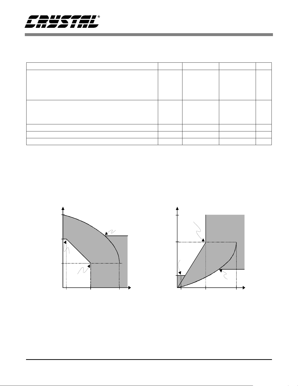
Parameter Symbol Min Max Unit
Switching Current High (Note 5)
0 < Vout < 1.4
1.4 < Vout < 2.4
I
OH
-44
-
-
mA
mA
-
3.1 < Vout < 3.3
Switching Current Low (Note 5)
Vout > 2.2
2.2 > Vout > 0.55
0.71 > Vout > 0
Low Clamp Current -5 < Vin < -1 I
I
OL
CL
95
Vout/0.023
-
-mA
Note 7
-
-
Note 8
mA
mA
Output rise slew rate 0.4 V - 2.4 V load (Note 6) slewr 1 5 V/ns
Output fall slew rate 2.4 V - 0.4 V load (Note 6) slewf 1 5 V/ns
Notes: 4. Specifications guaranteed by characterization and not production testing.
5. Refer to V/I curves in Figure 1. Specification does not apply to PCICLK and RST# signals. Switching
Current High specification does not apply to SERR#, PME#, and INTA# which are open drain outputs.
6. Cumulative edge rate across specified range. Rise slew rates do not apply to open drain outputs.
7. Equation A: I
8. Equation B: I
= 11.9 * (Vout - 5.25) * (Vout + 2.45) for 3.3 V > Vout > 3.1 V
OH
= 78.5 * Vout * (4.4 - Vout) for 0 V < Vout < 0.71 V
OL
DC
drivepoint
AC drive
point
Pull Up
-
Current(mA)
44
voltage
3.3
2.4
1.4
-2
EquationA:
I =11.9*(Vout-5.25)*(Vout+2.45)
OH
for 3.3V > Vout > 3.1V
voltage
test
po in t
0.55
176
-
Figure 1. AC Characteristics
Pull Down
3.3
AC drive
point
2.2
DC drive
point
3, 6 95 380
Equation B:
I = 78.5*Vout*(4.4-Vout)
OL
Current(mA )
for 0V < Vout < 0.71V
test
point
DS445PP1 5
Page 6
CS4630
DC CHARACTERISTICS (T
= 0° to 70° C; PCIVDD = CRYVDD = 3.3 V; CVDD = 2.5 V; VDD5REF =
A
5 V; PCIGND = CGND = CRYGND = 0 V; all voltages with respect to 0 V unless otherwise noted)
Parameter Symbol Min Typ Max Unit
PCI Interface Signal Pins
High level input voltage V
Low level input voltage V
High level output voltage Iout = -2 mA V
Low level output voltage Iout = 3 mA, 6 mA (Note 9) V
High level leakage current Vin = 2.7 V (Note 10) I
Low level leakage current Vin = 0.5 V (Note 10) I
IH
IL
OH
OL
IH
IL
2-5.75V
-0.5 - 0.8 V
2.4 - - V
--0.55V
--70µA
---70µA
Non-PCI Interface Signal Pins (Except XTALO)
High level input voltage XT ALI
Other Pins
Low level input voltage XTALI
Other Pins
V
IH
V
IL
2.3
2
-0.5
-0.5
3.3
-
0
-
(Note 14)
High level output voltage Iout = -3.5 mA (Notes 11, 12) V
Low level output voltage Iout = 3.5 mA (Note 12) V
High level leakage current Vin = 5.25 V (Note 12) I
Low level leakage current Vin = 0 (Note 12) I
OH
OL
IH
IL
2.4 - - V
--0.4V
--10µA
---10µA
4.0
5.75
0.8
0.8
V
V
V
V
Parameter Min Typ Max Unit
Power Supply Pins (Outputs Unloaded)
Power Supply Current: VDD5REF
PCIVDD/CRYVDD Total( (Notes 4,13)
CVDD
-
-
-
TBD
TBD
TBD
-
TBD
mA
mA
Low Power Mode Supply Current - TBD - mA
Notes: 9. The following signals are tested to 6 mA: FRAME#, TRDY#, IRDY#, DEVSEL#, STOP#, SERR#,
PERR#, and INTA#. All other PCI interface signals are tested to 3 mA.
10. Input leakage currents include hi-Z output leakage for all bi-directional buffers with three-state outputs.
11. For open drain pins, high level output voltage is dependent on external pull-up used and number of
attached gates.
12. All inputs that do not include internal pull-ups or pull-downs, must be externally driven for proper
operation. If an input is not driven, it should be tied to power or ground, depending on the particular
function. If an I/O pin is not driven and programmed as an input, it should be tied to power or ground
through its own resistor.
13. Typical values are given as average current with typical SP task execution and data streaming. Current
values vary dramatically based on the software running on the SP.
14. Vih for the Joystick position inputs (JACX JACY JBCX JBCY) is dependent on the joystick rate.
6 DS445PP1
Page 7
CS4630
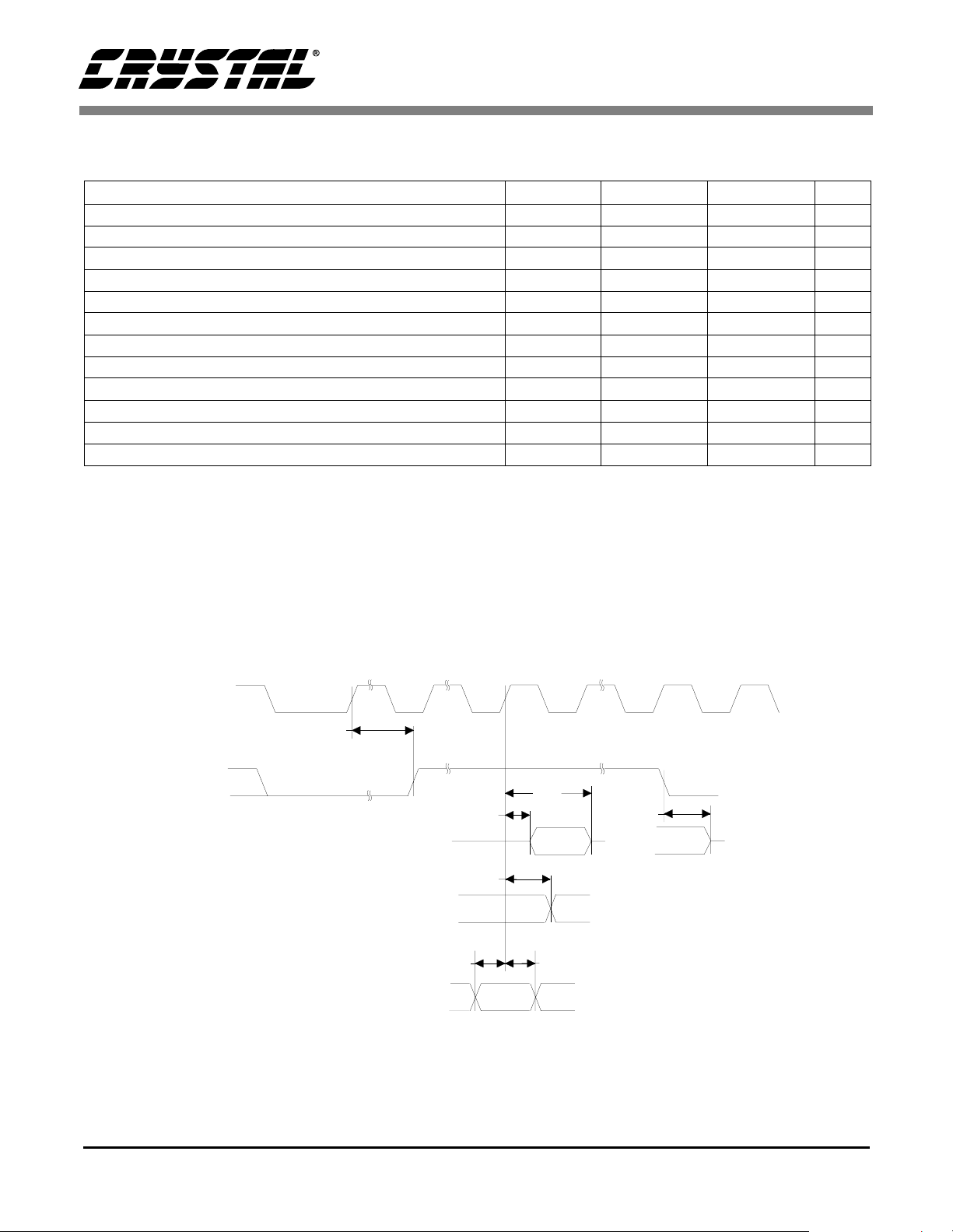
PCI INTERFACE PINS (T
=0° to 70° C; PCIVDD = CRYVDD = 3.3 V; CVDD = 2.5 V; VDD5REF = 5 V;
A
PCIGND = CGND = CRYGND = 0 V; Logic 0 = 0 V, Logic 1 = 3.3 V; Timing reference levels = 1.4 V)
Parameter Symbol Min Max Unit
PCICLK cycle time t
PCICLK high time t
PCICLK low time t
PCICLK to signal valid delay - bused signals (Note 18) t
PCICLK to signal valid delay - point to point (Note 18) t
val(p+p)
Float to active delay (Note 15) t
Active to Float delay (Note 15) t
Input Set up Time to PCICLK - bused signals (Note 18) t
Input Set up Time to PCICLK - point to point (Note 18) t
su(p+p)
Input hold time for PCICLK t
Reset active time after PCICLK stable (Note 16) t
rst-clk
Reset active to output float delay (Notes 15, 16, 17) t
cyc
high
low
val
on
off
su
h
rst-off
30 - ns
11 - ns
11 - ns
211ns
212ns
1-ns
-28ns
7-ns
10, 12 - ns
0-ns
100 -
µ
s
-30ns
Notes: 15. For Active/Float measurements, the Hi-Z or “off” state is when the total current delivered is less than or
equal to the leakage current. Specification is guaranteed by design, not production tested.
16. RST# is asserted and de-asserted asynchronously with respect to PCICLK.
17. All output drivers are asynchronously floated when RST# is active.
18. REQ# and GNT# are point to point signals. All other PCI signals are considered bused signals.
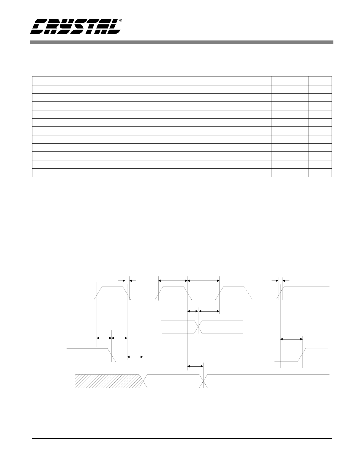
PCICLK
RST#
t
rst-clk
t
off
t
on
OUTPUTS
Hi-Z
t
val
OUTPUTS
Valid
INPUTS
t
su
Valid
Input
t
h
Figure 2. PCI Timing Measurement Conditions
t
rst-off
DS445PP1 7
Page 8
CS4630
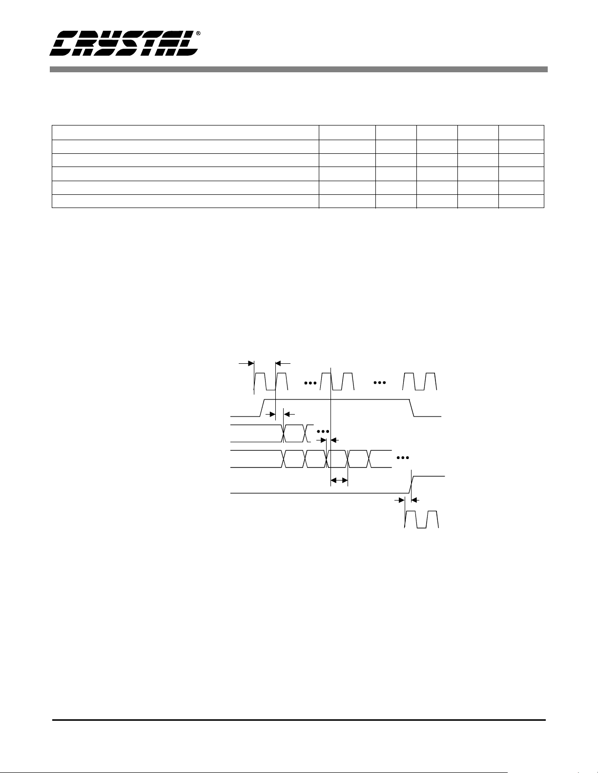
AC ’97 SERIAL INTERFACE TIMING (T
V;VDD5REF = 5 V; PCIGND = CGND = CRYGND = 0 V; Logic 0 = 0 V, Logic 1 = 3.3 V;
Timing reference levels = 1.4 V; unless otherwise noted)
Parameter Symbol Min Typ Max Unit
ABITCLK/ABITCLK2 cycle time t
ABITCLK/ABITCLK2 rising to ASDOUT/ADSOUT2 valid t
ASDIN/ASDIN2 valid to ABITCLK/ABITCLK2 falling t
ASDIN/ASDIN2 hold after ABITCLK/ABITCLK2 falling t
PCICLK rising to ARST#/ARST2# valid t
ABITCLK/ABITCLK2
= 0 to 70° C; PCIVDD = CRYVDD = 3.3 V; CVDD = 2.5
A
78 81.4 - ns
-1725ns
10 - - ns
5--ns
-10- ns
t
aclk
pd5
s5
h5
pd6
aclk
ASYNC/ASYNC2
ASDOUT/ASDOUT2
ASDIN/ASDIN2
ARST#/ARST2#
PCICLK
Figure 3. AC ’97 Configuration Timing Diagram
t
pd5
t
s5
t
h5
t
pd6
8 DS445PP1
Page 9
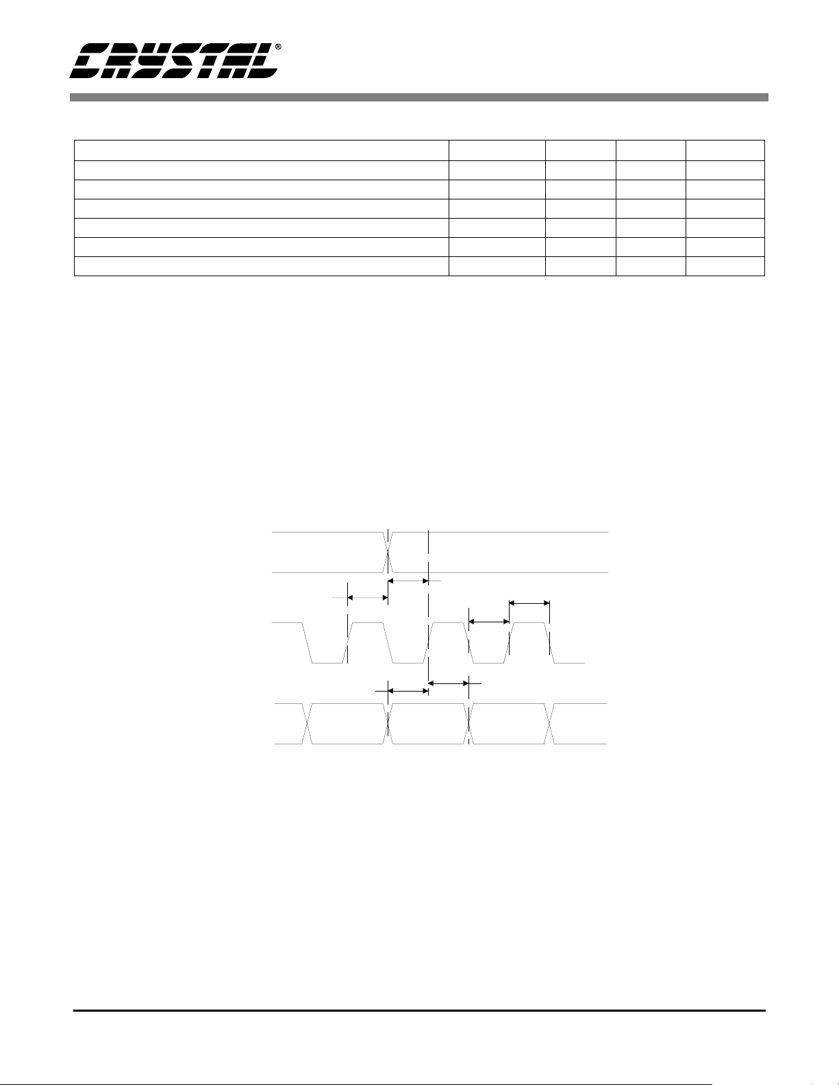
ZV PORT TIMING
Parameter Symbol Min Max Unit
ZLRCK delay after ZSCLK rising t
ZLRCK setup before ZSCLK rising t
ZSCLK low period t
ZSCLK high period t
ZSDATA setup to ZSCLK rising t
ZSDATA hold after ZSCLK rising t
slrd
slrs
sclk
sclkh
sdlrs
sdh
CS4630
2-ns
32 - ns
22 - ns
22 - ns
32 - ns
2-ns
ZLRCK
ZSCLK
ZSDATA
t
slrd
t
sdlrs
Figure 4. ZV PORT
t
slrs
t
sclkl
t
sdh
t
sclkh
DS445PP1 9
Page 10
CS4630
INDEPENDENT TIMING ENVIRONMENT (T
= 0 to 70° C; PCIVDD = CRYVDD = 3.3 V; CVDD =
A
2.5V; VDD5REF = 5 V; PCIGND = CGND = CRYGND = 0 V; Logic 0 = 0V, Logic 1 = 3.3 V;
Timing reference levels = 1.4 V; XTALI = 12.288 MHz; unless otherwise noted)
Parameter Symbol Min Typ Max Units
SCLK output cycle time t
FSYNC output cycle time (@SCLK falling edge) t
SCLK falling to FSYNC transition t
LRCLK output cycle time (@ SCLK rising edge) t
SCLK rising to LRCLK transition t
SCLK falling to SDOUT/SDO2/SDO3 valid t
SDIN/SDIN2 valid to SCLK rising (SI1F2-0: 010, SI2F1-0: 00) t
SDIN/SDIN2 hold after SCLK rising
sclk
fsync
pd7
lrclk
pd8
pd9
s6
t
h6
312 326 - ns
20000 20833 - ns
-45 2 45 ns
20000 20833 - ns
-45 2 45 ns
- 2 45 ns
30 - - ns
30 - - ns
(SI1F2-0: 010, SI2F1-0: 00)
SDIN/SDIN2 valid to SCLK falling
t
s7
30 - - ns
(SI1F2-0: 011, SI2F1-0: 01)
SDIN/SDIN2 hold after SCLK falling
t
h7
30 - - ns
(SI1F2-0: 011, SI2F1-0: 01)
XTAL frequency 12.287 12.288 12.289 MHz
XTALI high time (Note 4) 35 - - ns
XTALI low time (Note 4) 35 - - ns
MCLK output frequency (Note 4) 12.287 12.288 12.289 MHz
SCLK
FSYNC
LRCLK
SDOUT/SD02/SD03
SDIN/SDIN2
SDIN/SDIN2
t
sclk
t
18
fsync
t
lrclk
15
0
0
0
t
pd7
t
pd8
t
pd9
15
t
s6
16 0
17
t
t
s7
19
18 0
h6
t
h7
0
17 16
19
Figure 5. Independent Timing Configuration
10 DS445PP1
Page 11
CS4630
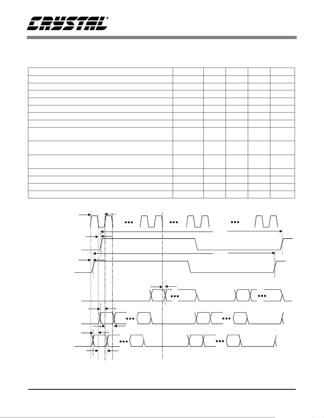
EEPROM TIMING CHARACTERISTICS (T
= 0 to 70 °C, PCIVDD = CRYVDD = 3.3 V; CVDD =
A
2.5V; VDD5REF = 5 V; PCIGND = CGND = CRYGND = 0 V; Logic 0 = 0 V, Logic 1 = 3.3 V;
Timing reference levels = 1.4 V; PCI clock frequency = 33 MHz; unless otherwise noted (Note 4))
Parameter Symbol Min Max Units
EECLK Low to EEDAT Data Out Valid t
Start Condition Hold Time t
EECLK Low t
EECLK High t
Start Condition Setup Time (for a Repeated Start Condition) t
EEDAT In Hold Time t
EEDAT In Setup Time t
HD:STA
LEECLK
HEECLK
SU:STA
HD:DAT
SU:DAT
EEDAT/EECLK Rise Time (Note 19) t
EEDAT/EECLK Fall Time t
Stop Condition Setup Time t
SU:STO
EEDAT Out Hold Time t
AA
R
F
DH
07.0
5.0 10 10 -
5.0 -
0-
250 - ns
-1
- 300 ns
5.0 -
0-
µ
s
µ
s
µ
s
µ
s
µ
s
µ
s
µ
s
µ
s
µ
s
Notes: 19. Rise time on EEDAT is determined by the capacitance on the EEDAT line with all connected gates and
the required external pull-up resistor. Nominal values based on 4.7k and 22pF.
t
t
F
HEECLK
t
LEECLK
t
R
EECLK
t
HD:DAT
t
SU:DAT
EEDAT (IN)
EEDAT (OUT)
t
SU:STA
t
HD:STA
t
AA
t
SU:STO
t
DH
EEDAT (OUT)
Figure 6. EEPROM Timi n g
DS445PP1 11
Page 12
CS4630
2. OVERVIEW
The CS4630 is a high performance audio accelerator DSP for the PCI bus. This device, combined
with application and driver software, provides a
complete system solution for cost effective acceler-
ation of Microsoft’s DirectSound,
Direct Sound3D, DirectInput, MIDI playback via
Wavetable Synthesis with reverberation and chorus
effects processing, and more. The following features can be enabled via updated device driver:
• Primary AC ‘97 Interface now 2.1 compatible
• 2nd AC ‘97 codec support
• Increased on-board memory for enhanced algorithm execution and greater concurrency
• 128 DMA Streams Supported
• PCI Power Management Event Support(D0D3
• Support for wake-up event via AC 97 2.1 Link
There are three main functional blocks within the
CS4630: the Stream Processor, the PCI Interface,
and the DMA Engine. A block diagram of the
CS4630 device is shown in Figure 7. The Stream
Processor (SP) is a high speed custom Digital Signal Processor (DSP) core specifically designed for
cold
)
audio signal processing. This extremely powerful
DSP core is capable of running complex algorithms
and a number of different signal processing algorithms simultaneously. This high concurrency capability is valuable for applications such as immersive
3D games, which may play a nu mber of DirectSound
streams, a number of DirectSound3D streams, and a
MIDI music sequence simultaneously.
Separate RAM memories are included on-chip for
the SP program code (PROGRAM RAM), parameter data (PARAMETER RAM), and audio sample
data (SAMPLE RAM). Two ROM memories store
coefficients for sample rate conversion and audio
decompression algorithms (COEFFICIENT ROM)
and common algorithm code (PROGRAM ROM).
The RAM-based DSP architecture of the CS4630
ensures maximum system flexibility. The software
function/feature mix can be adapted to meet the requirements of a variety of different applications,
such as DirectX games, DVD movie playback, or
DOS applications. This RAM-based architecture
also provides a means for future system upgrades,
28-Stream
1
DMA Controller
with Hardware
Scatter/Gather
PC/PCI &
PCI
Interfac e
12 DS445PP1
CCLS Legacy
MPU-401
MIDI Interface
Joystick
Interfa c e
Figure 7. CS4630 Block Diagram
Parameter
RAM
Sample
RAM
Program
RAM
Program
ROM
Coefficient
ROM
SLIMD
SP Core
Dual Codec
AC ’97 2.1
Interface
EGPIO
S/PDIF In
S/PDIF Out
ZV Port
Async. Serial
Port Interface
Page 13

CS4630
allowing the addition of new or upgraded functionality through software updates.
The CS4630 provides an extremely efficient bus
mastering interface to the PCI bus. The PCI Interface function allows economical burst mode transfers of audio data between host system memory
buffers and the CS4630 device. Program code and
parameter data are also transferred to the CS4630
over the PCI interface.
The DMA Engine provides dedicated hardware to
manage transfer of up to 128 concurrent audio/data
streams to and from host memory buffers. The
DMA Engine provides hardware scatter-gather
support, allowing simple buffer allocation and
management. This implementation improves system efficiency by minimizing the number of host
interrupts.
The CS4630 supports a variety of audio I/O configurations including a single CS4297/97A/98/99
CrystalClear AC ’97 Codec or dual
CS4297/97A/98/99 codecs where the second codec
is used to support 4-Channel audio or resides in a
portable’s docking station. The system’s flexibility
is further enhanced by the inclusion of a bi-directional serial MIDI port, a joystick port, a hardware
volume control interface, a ZV Port interface, and
a serial data port which allows connection of an optional external EEPROM device.
2.1 Stream Processor DSP Core
Multiply-Accumulate (MAC) blocks and one 16bit Arithmetic and Logic Unit (ALU). The SP core
is conservatively rated at 420 Million Instructions
per second (420 MIPS) when running at an 140
MHz internal clock speed. The MAC units perform
dual 20-bit by 16-bit multiplies and have 40-bit accumulators, providing higher quality than typical
16-bit DSP architectures.
A programmable Phase Locked Loop (PLL) circuit
generates the high frequency internal SP clock
from a lower frequency input clock. The input to
the PLL may be from a crystal oscillator circuit or
the serial port clock ABITCLK/SCLK. Clock control circuitry allows gating of clocks to various internal functional blocks to conserve power during
power conservation modes, as well as during normal modes of operation when no tasks are being
executed.
2.2 Legacy Support
Legacy games are supported by CrystalClear Legacy Support (CCLS), DDMA, or PC/PCI interface.
In both motherboard and add-in card designs,
CCLS and DDMA provide support for legacy
games by providing a hardware interface that supports a Sound Blaster Pro compatible interface, as
well as support for FM, MPU-401, and joystick interfaces. These hardware interfaces provide PCIonly games compatibility for real-mode DOS and
Windows DOS box support.
The CS4630 Stream Processor (SP) is a custom
DSP core design which is optimized for processing
and synthesizing digital audio data streams. The SP
features a Somewhat Long Instruction Multiple
Data (SLIMD) modified dual Harvard architecture.
The device uses a 40-bit instruction word and operates on 32-bit data words. The SP includes two
DS445PP1 13
For motherboard designs, PC/PCI can be used by
connecting the PCGNT# and PCREQ# pins to the
appropriate pins on the south bridge motherboard
chip. The PC/PCI interface is compliant with Intel’s PC/PCI spec. (version 1.2). The BIOS must
enable the PC/PCI mechanism at boot time on both
the CS4630 and the south bridge.
Page 14

CS4630
3. SYSTEM ARCHITECTURES
A typical system diagram depicting connection of
the CS4630 to the CrystalClear CS4297/97A/98/99
AC ’97 Codec is given in Figure 8. All analog audio inputs and outputs are connected to the
CS4297/97A/98/99. Audio data is passed between
the CS4297/97A/98/99 and the CS4630 over the
serial AC-Link. The CS4630 provides a hardware
interface for connection of a joystick and MIDI devices. A second diagram, Figure 9, depicts the
CS4630 supporting dual AC ‘97 codecs in a portable design. The AC ‘97 interface is connected to the
primary AC ‘97 codec in the portable and is used
for all audio I/O inside and connected to the porta-
CPU
North
Bridge
PCI Bus
ble. The AC ‘97 interface is sent across to the docking station which contains a second AC ‘97 2.0/2.1
codec, used when the portable is in the docking station. Software can disable the audio I/O paths on
the portable that are superseded by docking station
I/O and enable th e paths n eed ed in the do cking s tation. Note that both interfaces are needed in systems where the CD-ROM analog input is in the
portable and the Line In/Out jacks on the docking
stations are used. Using the AC ‘97 digital link
across the dock maintains the absolute highest audio quality along with a standard well-defined nonproprietary interface that will last through many
system generations.
Host
Memory
PORTABLE
CPU
South
Bridge
Card Bus
Interface
South
Bridge
PC/PCI (if used)
CS4630
Figure 8. AC ‘97 Codec Interface
North
Bridge
PCI Bus
Audio
Accelerator
CS4630
PC/PCI
(if used)
ZV Port
Host
Memory
Bridge
Pri. AC ’97
Codec
Audio
Out
Audio
CS4297
In
Audio Out
Audio In
DOCKING STATION
Secondary PCI Bus
Sec. AC ’97
Codec
Audio Out
Audio In
Figure 9. Portable Docking Station Scenario
14 DS445PP1
Page 15

CS4630
4. HOST INTERFACE
The CS4630 host interface is comprised of two separate interface blocks which are memory mapped
into host address space. The interface blocks can be
located anywhere in the host 32-bit physical address space. The interface block locations are defined by the addresses programmed into the two
Base Address Registers in the PCI Configuration
Space. These base addresses are normally set up by
the system’s Plug and Play BIOS. The first interface block (located by Base Address 0) is a 4 kByte
register block containing general purpose configuration, control, and status registers for the device.
The second interface block (located by Base Address 1) is a 1 MByte block which maps all of the
internal RAM memories (SP Program RAM, Parameter RAM, and Sample RAM) into host m emory space. This allow s the h ost to direct ly peek and
poke RAM locations on the device. The relationship between the Base Address Registers in the
CS4630 PCI Configuration Space and the host
memory map is depicted in Figure 10.
The bus mastering PCI bus interface complies with
the PCI Local Bus Specification (version 2.1).
4.1 PCI bus Transactions
As a target of a PCI bus transaction, the CS4630
supports the Memory Read (from internal registers
or memory), Memory Write (to internal registers or
memory), Configuration Read (from CS4630 configuration registers), Configuration Write (to
CS4630 configuration registers), Memory Read
Multiple (aliased to Memory Read), Memory R ead
Line (aliased to Memory Read), the Memory Write
and Invalidate (aliased to Memory Write) transfer
cycles, and I/O Read, I/O Write cycles (for legacy
audio support). The Interrupt Acknowledge, Special Cycles, and Dual Address Cycle tr ansactions
are not supported.
As Bus Master, the CS4630 generates the Memory
Read Multiple, Memory Write, I/O Read and I/O
Write transactions. The Memory Read, Configuration Read, Configuration Write, Memory Read
Line, Memory Write and Invalidate, Interrupt Ac-
Device PCI Con fig. Space
00h
04h
08h
0Ch
10h
14h
DS445PP1 15
Device ID / Vendor ID
Status / Command
Class Code / Revision
Misc. Control
Base Address Register 0
Base Address Register 1
Figure 10. Host Interface Base Address Registers
Direct I/O Regis t ers
(Memory Mapped, 4 kByte)
Direct Memory Inter face
(Memory Mapped, 1 MByte)
Page 16

CS4630
knowledge, Special Cycles, and Dual Address Cycle transactions are not generated.
The PCI bus transactions supported by the CS4630
device are summarized in Table 1. Note that no
Target Abort conditions are signalled by the device. Byte, Word, and Doubleword transfers are
supported for Configuration Space accesses. Only
Doubleword transfers are supported for Register or
Memory area accesses. Bursting is not supported
for host-initiated transfers to/from the CS4630 internal register space, R AM memory space, or P CI
configuration space (disconnect after first phase of
transaction is completed).
Initiator Target Type PCI Dir
Host Registers (BA0) Mem Write
Host Registers (BA0) Mem Read
Host Memories (BA1) Mem Write
Host Memories (BA1) Mem Read
Host Config Space 1 Config Write
Host Config Space 1 Config Read
Host Legacy H/W I/O Write
Host Legacy H/W I/O Read
CS46XX Host System Mem Write
CS46XX Host System Mem Read
CS46XX South Bridge I/O Write
CS46XX South Bridge I/O Read
Table 1. PCI Interface Transaction Summary
In
Out
In
Out
In
Out
In
Out
Out
In
Out
In
16 DS445PP1
Page 17

CS4630
4.2 Configuration Space
The content and format of the PCI Configuration Space is given in Table 2.
Byte 3 Byte 2 Byte 1 Byte 0 Offset
Device ID: R/O, 6003h Vendor ID: R/O, 1013h 00h
Status Register, bits 15-0:
Bit 15 Detected Parity Error: Error Bit
Bit 14 Signalled SERR: Error Bit
Bit 13 Received Master Abort: Error Bit
Bit 12 Received Target Abort: Error Bit
Bit 11 Signalled Target Abort: Error Bit
Bit 10-9 DEVSEL Timing: R/O, 10b (slow)
Bit 8 Data Parity Error Detected: Error Bit
Bit 7 Fast Back to Back Capable: R/O 0
Bit 6 User Definable Features: R/O 0
Bit 5 66MHz Bus: R/O 0
Bit 4 New Capabilities: R/O 1
Bit 3-0Res erved: R/O 0000
Reset Status State: 0410h
Write of 1 to any error bit position clears it.
Class Code: R/O 040100h
Class 04h (multimedia device), Sub-class 01h (audio), Interface 00h
BIST: R/O 0 Header Type:
Bit 7: R/O 0
Bit 6-0: R/O 0 (type 0)
Base Address Register 0
Device Control Register space, memory mapped. 4 kByte size
Bit 31-12: R/W, default 0. Compare address for register space accesses
Bit 11 - 4: R/O 0, specifies 4 kByte size
Bit 3: R/O 0, Not Prefetchable (Cacheable)
Bit 2-1: R/O 00, Location Type - Anywhere in 32 bit address space
Bit 0: R/O 0, Memory space indicator
Command Register, bits 15-0:
Bit 15-10: Reserved, R/O 0
Bit 9 Fast B2B Enable: R/O 0
Bit 8 SERR Enable: R/W, default 0
Bit 7 Wait Control: R/O 0
Bit 6 Parity Error Response: R/W, default 0
Bit 5 VGA Palette Snoop: R/O 0
Bit 4 MWI Enable: R/O 0
Bit 3 Special Cycles: R/O 0
Bit 2 Bus Master Enable: R/W, default 0
Bit 1 Memory Space Enable: R/W, default 0
Bit 0 IO Space Enable: R/O 0
Latency Timer:
Bit 7-3: R/W,default 0
Bit 2-0: R/O 0
04h
Revision ID: R/O 01h 08h
Cache Line Size:
R/O 0
0Ch
10h
Base Address Register 1
Device Memory Array mapped into host system memory space, 1 MByte size
Bit 31-20: R/W, default 0. Compare address for memory array accesses
Bit 19 - 4: R/O 0, specifies 1 MByte size
Bit 3: R/O 0, Not Prefetchable (Cacheable)
Bit 2-1: R/O 00, Location Type - Anywhere in 32 bit address space
Bit 0: R/O 0, Memory space indicator
Base Address Register 2: R/O 0000000 0h, Unus ed 18h
Base Address Register 3: R/O 0000000 0h, Unus ed 1Ch
Base Address Register 4: R/O 0000000 0h, Unus ed 20h
Base Address Register 5: R/O 0000000 0h, Unus ed 24h
Cardbus CIS Pointer: R/O 00000000h, Unused 28h
Table 2. PCI Co nf iguration Space
DS445PP1 17
14h
Page 18

CS4630
Byte 3 Byte 2 Byte 1 Byte 0 Offset
Subsystem ID
R/O Defaults to 0000h if EEPROM is not present,
otherwise loaded from the EEPROM.
Writable via Configuration Space Offset 0xFEh
or BA0:4B4h.
Expansion ROM Base Address: R/O 00000000h, Unused 30h
Reserved: R/O 00000000h 34h
Reserved: R/O 00000000h 38h
Max_Lat: R/O 18h
24 x 0.25uS = 6 uS
PMC
Bit 15: PME# from D3cold: R/O 0(default) or
1(configurable)
Bit 14: PME# from D3hot: R/O 0(default) or
1(configurable)
Bit 13: PME# from D2: R/O 0(default) or
1(configurable)
Bit 12: PME# from D1: R/O 0(default) or
1(configurable)
Bit 11: PME# from D0: R/O 0(default) or
1(configurable)
Bit 10: D2 support: R/O 1
Bit 9: D1 support: R/O 1
Bit 8-6:Aux Current: R/O 000(default) or configurable
Bit 5: Device Specific init: R/O 1
Bit 4: Auxiliary power: R/O 0
Bit 3: PME# clock: R/O 0
Bit 2-0: Version: R/O 010
Min_Gnt: R/O 04h
4 x 0.25uS = 1uS
Subsystem Vendor ID
R/O Defaults to 0000h if EEPROM is not
present, otherwise loaded from the EEPROM.
Writable via Configuration Space Offset 0xFCh
or BA0:4B4h.
Interrupt Pin:
R/O 01h, INTA used
Next Item Pointer:
R/O 0h
Interrupt Line:
R/W, default 0
Capability ID:
R/O 1h
2Ch
3Ch
40h
PMCSR
Bit 15: PME# status: R/W 0
Bit 14-13: Data scale: R/O 00
Data: R/O 0 PMCSR_BSE: R/O 0
Dynamic Config Register
Bit 31: PME Support Shadow bit: R/W 0
Bit 30: Reserved: R/W 0
Bits 29-27: Aux Current Shadow bits: R/O 000
Bits 26-24: Reserved: R/O 000
Bits 23-16: Dynamic CNFG bits 23-16: R/W 0h
Subsystem ID shadow register
0FEh W/O shadow Subsystem ID (0x2E)
Table 2. PCI Configuration Space
18 DS445PP1
Bit 12-9: Data select: R/O 0000
Bit 8: PME_En: R/W 0
Bit 7-2: Reserved: R/O 000000
Bit 1-0: Power state: R/W 00
Dynamic Config Register
Bits 15-0: Dynamic CNFG bits 15-0: R/W 0h
Subsystem Vendor ID shadow register
0FCh W/O shadow Subsystem ID (0x2C)
(cont.)
44h
F8h
FCh
Page 19

CS4630
4.3 Subsystem Vendor ID Fields
The Subsystem ID and Subsystem Vendor ID configuration fields can be loaded in two different
ways. For systems using an EEPROM, typically
add-in cards, the EEPROM auto loads the data. For
a system using BIOS, typically mother boards, the
Configuration Space is loaded at offset FCh (see
Table 2). Once these values are loaded they will appear in the Configuration Space offset 2Ch. The
Subsystem ID and Subsystem Vendor ID fields in
the PCI Configuration Space default to value
0000h unless an external EEPROM device is detected or unless the host has written to the appropriate internal register to program the values.
4.4 Dynamic Config Register
The Dynamic Configuration Register is primarily
used to configure the hardware to support the generation of the PME# signal to the PCI bus and store
the particular hardware configuration. Bit 31,
PME_Support Shadow, shadows bits 14-11 of the
configuration space PMC Register at offset 42h.
Bits 29-27 will shadow bits 8-6 of the PMC Register if the Vaux_Sense pin is high indicating auxillary power is available. Otherwise, bits 8-6 will be
set to ‘000’b. Bits 23-0 are general purpose
Read/Write bits and the definitions will be determined by the driver.
The Dynamic Configuration Register bits can be
loaded in two different ways. For systems using an
EEPROM typically add-in cards, the EEPROM
auto loads the data. For a system using BIOS, typically mother boards, the Dynamic Configuration
Register is loaded at offset F8h (see Table 2). The
Dynamic Configuration Register bits will default to
value 0000h unless an external EEPROM device is
detected or unless the host has written to the appropriate internal register to program the values.
4.5 Interrupt Signal
The CS4630 PCI Interface includes an interrupt
controller function which receives interrupt requests from multiple sources within the CS4630
device, and presents a single interrupt line (INTA)
to the host system. Interrupt control registers in the
CS4630 provide the host interrupt service routine
with the ability to identify the source of the interrupt and to clear the interrupt sources. In the
CS4630, the single external interrupt is expanded
by the use of “virtual channels”. Each data st ream
which is read from or written to a modular buffer is
assigned a virtual channel number. This virtual
channel number is signalled by the DMA subsystem anytime the associated modular buffer
pointer passes the mid-point or wraps around. Virtual channels are also used for message passing between the CS4630 and the host.
DS445PP1 19
Page 20

CS4630
5. SERIAL PORT CONFIGURATIONS
A flexible serial audio interface is provided which
allows connection to external Analog-to-Digital
Converters (ADCs), Digital-to-Analog Converters
(DACs) or Codecs (combined ADC and DAC
functions) in several different configurations. The
serial audio interface includes a primary input/output port with dedicated serial data pins (SDIN, SDOUT), two auxiliary audio output ports (SDO2,
SDO3) which share pins with the joystick interface
button input functions, and one auxiliary audio input port (SDIN2). Each of these digital audio input
and output pins carry two channels of audio data.
These two channels may comprise the left and right
channels of a stereo audio signal, or two independent monaural audio signals.
Each digital audio channel is internally buffered
through a 16 sample x 20-bit FIFO. The data format
for the serial digital audio ports varies depending
on the configuration. The primary configuration includes a CS4630 plus a CS4297/97A/98/99.
The CS4630 communicates with the
CS4297/97A/98/99 over the AC-link as specified
in the Intel‚ Audio Codec ‘97 Specification (r evision 2.1). A block diagram for the AC ’97 Controller configuration is given in Figure 11. In this
configuration, the AC ’97 Codec is the timing master for the digital audio link. The ASDOUT output
supports data transmission on all ten possible sample slots (output slots 3 - 12). The ASDIN input
supports receiving of audio sample data on all input
sample slots (input slots 3 - 12). The SDO2 and
SDO3 serial outputs and the SDIN2 serial input are
not supported in this configuration. In the dual AC
‘97 system, the primary AC ‘97 codec is connected
as in the single codec case; however, a second
CS4297A/98/99 is connected to a completely separate serial data in pin ASDIN2. A block diagram
ABITCLK
ASYNC
ASDOUT
ASDIN
ARST#
CS4630
MIDIIN
MIDIOUT
JACX, JACY, JBCX, JBCY
JAB1, JAB2, JBB1, JBB2
Figure 11. AC ‘97 Codec Connection Diagram
12.288 MHz
48 kHz
24.576 MHz
BIT_CLK
SYNC
SDATA_OUT
SDATA_IN
RESET#
CS429
7A
Joystick/
MIDI Por t
Analog Interface
20 DS445PP1
Page 21

CS4630
depicting the Dual AC ’97 codec configuration as a
docking station is given in Figure 9. In this scenario, the first codec is used in the portable for traditional functions such as analog support for the
portable’s Line In, Mic In, and Line Out jacks. The
AC Link to the dock is buffered and sent across to
the docking station to support a second
CS4297A/98/99 that supports the dock’s analog
jacks. When the system gets a message that the
docking station is attached, the software can replace the portable’s analog jack control for the
docking station’s jacks seemlessly. Using a standard AC Link for the docking station support maintains the highest quality of audio over analog
ABITCLK
ASYNC
ASDOUT
ASDIN
ARST#
12.288 MHz
48 kHz
docking station scenarios. In addition, since the AC
Link is a standard, the docking station can be utilized over a number of portable generations without concern for obsolescence.
The signal connections between the CS4630 and
the dual Codecs are shown in Figure 12. In this
configuration, both AC ‘97 codecs run off the same
ABITCLK with the primary AC ’97 Codec being
the timing master for the first AC Link and for the
CS4630. The secondary CS4297/97A/98/99 and
the CS4630 are slaves to the incoming ABITCLK.
Full FIFO buffers for both codecs are supported.
BIT_CLK
SYNC
SDATA_OUT
SDATA_IN
RESET#
CS4630
ASDIN2
MIDIIN
MIDIOUT
JACX, JACY, JBCX, JBCY
JAB1, JAB2, JBB1, JBB2
Figure 12. Dual AC ‘97 Codec Connection Diagram
24.576 MHz
CS4297/97A/99
BIT_CLK
SYNC
SDATA_OUT
SDATA_IN
RESET#
Secondary
AC’97 2.0 Codec
Joystick/
MIDI Port
Analog Interface
Analog Interface
DS445PP1 21
Page 22

CS4630
6. GAME PORT
6.1 MIDI Port
In the AC ’97 controller c onfiguration, a bi-directional MIDI interface is provided to allow connection of external MIDI devices. The MIDI interface
includes 16-byte FIFOs for the MIDI transmit and
receive paths.
DSP
6.2 Joystick Port
In the AC ’97 controller configuration, a joystick
port is provided. The joystick port supports four
“coordinate” channels and four “button” channels.
The coordinate channels provide joystick positional information to the host, and the button channels
provide user button event information. The joystick
interface is capable of operating in the traditional
“polled” mode, but also provides a “hardware ac celerated” mode of operation wherein internal
counters are provided to assist the host with coordinate position determination. The Joystick schematic is illustrated in Figure 13.
+5 V
1
JAB1
JBB1
JACX
JBCX
5.6 nF
JBCY
JACY
JBB2
JAB2
4.7 k
MIDIOUT
MIDIIN
4.7 k
4.7 k
Ω
Ω
2.2 k
2.2 k
Ω
5.6 nF
1nF 1nF
4.7 k
Ω
2.2 k
2.2 k
Ω
5.6 nF 5.6 nF
Ω
Ω
4.7 k
Ω
Ω
1nF
1nF
9
2
10
3
11
4
12
5
13
6
14
7
15
8
Figure 13. Joystick Logic
22 DS445PP1
Page 23

CS4630
7. EEPROM INTERFACE
The EEPROM configuration interface allows the
connection of an optional external EEPROM device to provide power-up configuration information. The external EEPROM is not required for
proper operation; however, in some applications
power-up configuration settings other than the default values may be required to support specific operating system compatibility requirements.
After a hardware reset, an internal state mach ine in
the CS4630 will automatically detect the presence
of an external EEPROM device (assuming EEPDIS
is low) and load the Subsystem ID and Subsystem
Vendor ID fields, along with two bytes of general
configuration information, into internal registers.
At power-up, the CS4630 will attempt to read from
the external device, and will check the data received from the device for a valid signature header.
If the header data is invalid, the data transfer is
aborted. After power-up, the host can read or write
from/to the EEPROM device by accessing specific
registers in the CS4630. Cirrus Logic provides software to read and write the EEPROM.
The two-wire interface for the optional external
EEPROM device is depicted in Figure 14. During
data transfers, the data line (EEDAT) can change
state only while the clock signal (EECLK) is low.
A state change of the data line while the clock signal is high indicates a start or stop condition to the
EEPROM device.
The EEPROM device read access sequence is
shown in the Figure 15. The timing follows that of
a random read sequence. The CS4630 first per-
forms a “dummy” write operation, then generates a
start condition followed by the slave device address
and the byte address of zero. The CS4630 always
begins access at byte address zero and continues
access a byte at a time, using a sequential read, unt il
all needed bytes in the EEPROM are read. Si nce
only a maximum of 12 bytes are needed, the smallest EEPROM available will suffice.
CS46XX
EEPROM
SLIMD SP
Core
Ω
4.7 k
EEDAT
EECLK
Figure 14. External EEPROM Connection
Part
Start
Address
S10100000A00000000AS10100001A Data Data P1A
Write
Bank
Address
Figure 15. EEPROM Read Sequence
Start
Acknowledge Data
Part
Address
2-wire
Serial
EEPROM
Read
Acknowledge
No
Acknowledge
Stop
DS445PP1 23
Page 24

CS4630
8. GENERAL PURPOSE I/O PINS
Many of the CS4630 signal pins are internally multiplexed to serve different functions depending on
the environment in which the device is being used.
Several of the CS4630 signal pins may be used as
general purpose I/O pins when not required for other specific functions in a given application.
8.1 EGPIO
In addition to the GPIO pins on the CS4630, extended general purpose I/O has been added. Four
EGPIO pins are not multiplexed, EGPIO[7, 2:0];
whereas; EGPIO[6:3] are shared with the asynchronous serial port. When this second async. serial port is not used, all the EGPIO pins are available.
These pins have extended functionality in that any
EGPIO pin can be programmed to cause a power
management wake-up event on the PME# signal.
These pins also can be programmed as:
• input or output,
• edge or level sensitive (sticky),
• active high or low input,
• CMOS or open-drain output
9. ZV PORT SERIAL INTERFACE
The ZV PORT interface consists of three input
pins: ZLRCK, ZSCLK, and ZSDATA. ZLRCK is
the Left/Right clock indicating which channel is
currently being received. ZS CLK is the serial bit
clock where ZLRCK and ZSDATA change on the
falling edge and serial data is internally latched on
the rising edge. Note that the serial data starts one
ZSCLK period after ZLRCK transitions. Figu re 16
illustrates the clocking on the ZV PORT pins.
10.CONSUMER IEC-958 DIGITAL INTERFACE (S/PDIF)
The CS4630 supports the industry standard IEC958 consumer digital interface. Sometimes this
standard is referred to as S/PDIF, which refers to an
older version of this standard. This output provides
an interface, external to the PC, for storing digital
audio (as in a DAT or recordable CD-ROM) or
playing digital audio from digital speakers.
Figure 17 illustrates the circuit necessary for imp lementation of the IEC-958 consumer interface.
An external buffer is require d to drive the current
needed for the 75 Ω interface. A current driver is
implemented to increase the transmission range of
the coaxial circuitry.
Figure 18 illustrates an optional fiber optic circuit.
The optical circuit connects directly to the CS4630
and no additional current driver is needed.
ZLRCK
ZSCLK
ZSDATA
24 DS445PP1
15 14 13 12 11 10
Left Channel
6
7
54321098
Figure 16. ZV Port Clocking Format
15 14 13 12 11 10
Right Channel
654
87
32
109
Page 25

DGND
D
SPDIF I
SPDIFO
SN75179D
0.1
µ
F
2
3
+5 V PCI
1
VCC
GND
4
DGND
CS4630
21
IEC_958_RX
8
7
5
6
0.1
0.1
2
1
374
1
µ
F
2
µ
F
1
90.9
2
DGND DGND
J-RCA-RA-PCB
75
1
4
29398
1
2
DGND
IEC_958_TX
5
8
J-RCA-RA-PCB
1
2
Figure 17. IEC Consumer Interface Implementation Circuit
5
6
DGND
DGND
DGND
5
6
TOTX-173
4
+5V_PCI
SPDIFO
1 k
SPDIFI
8.2K
3
2
1
TOTX-173
+5V_PCI
.1µF
DGND
4
3
2
1
47 µH
1 µF
DGND
DGN
Figure 18. Optional Fiber Optic Circuit
DS445PP1 25
Page 26

CS4630
11.PCI POWER MANAGEMENT
The CS4630 supports the PCI Bus Power Management Interface Specification (version 1.1). The
CS4630 supports all power states and is capable of
PME# generation from D0 - D3
vided auxillary 3.3V power is available
The PCI power management specification defines
four major power states: D0 (fully on), D1, D2, and
D3 (fully off). The D3 state is divided into two substates, D3hot and D3cold. D3cold differs from
D3hot in that the normal PCI bus Vcc power sources are turned off.
11.1 D0 State
The D0 state is divided into two substates,
D0active and D0uninitialized. The D0unitialized
state describes a device that has just received a PCI
RST# signal and has not yet been programmed;
therefore, it is not consuming full power. The
D0active state describes a device that has been programmed and is fully operational.
The CS4630 must initially be put into D0 before
being used. Upon entering D0 from power on reset,
or transition from D3cold, the CS4630 will be in an
uninitialized state. Once initialized by the system
software, it will transition to the D0active state.
CS4630 Operation during D0 state:
• Phase Lock Loop - Running
• SP Clock - Running
• SP RAM Clock - Running
• AC Link - Running
11.2 Dl State
Dl is used as a light sleep state. All ne cessary internal state information and data samples are preserved while in D1. The transi tion back to D0 st ate
will occur within 100ms.
CS4630 Operation during D1 state:
• Phase Lock Loop - Running
• SP Clock - Stopped
• SP RAM Clock - Running
• AC Link - Running
, and D3
hot
cold
pro-
11.3 D2 State
This state requires significant power savings while
still retaining the abi1ity to recover to a previous
condition. The transition back to D0 state will occur within 100ms.
CS4630 Operation during D2 state:
• Phase Lock Loop - Running
• SP Clock - Stopped
• SP RAM Clock - Stopped
• AC Link - Running
11.4 D3
hot
State
In this state, function context need not be maintained. When the CS4630 is brought back to D0
(the only legal state transition from D3), software
will perform a full reinitialization of the CS4630
including its PCI Configuration Space.When programmed to D0 from D3, the CS4630 performs the
equivalent of a warm reset and returns to the
D0uninitialized state without PCI RST# being asserted.
CS4630 Operation during D3hot state:
• Phase Lock Loop - Stopped
• SP Clock - Stopped
• SP RAM Clock - Stopped
• AC Link - Stopped
11.5 D3
cold
State
When Vcc is removed from the PCI Bus and PCI
RST# is asserted, the CS4630 will transition immediately to D3cold. When power is restored, PCI
RST# will be de-asserted and the CS4630 will return to D0uninitialized state with a full PCI 2.1
compliant power on reset sequence whenever
PME# has not been enabled.
If the CS4630 is enabled to generate a PME# event
from the D3 power state, and an auxillary 3.3 V
power source is available, no logic within the chip
will be reset during the assertion of PCI RST#
while the main system 3.3 V is removed.
CS4630 Operation during D3cold state:
• Phase Lock Loop - Stopped
26 DS445PP1
Page 27

CS4630
• SP Clock - Stopped
• SP RAM Clock - Stopped
• AC Link - Stopped
11.6 CS4630 PME# Assertion
Two methods are supported by the CS4630 in generating a PME# event to the PCI Bus. Method one,
with ABITCLK running, is primarily used when
the SP is required to perform a processing task such
as discriminating a valid Ring condition from the
DAA or decode incoming Caller-ID information.
The other method is used when maximum power
savings is required (both ABITCLK and PCI CLK
are off) and the SP is not needed for signal processing.
11.6.1 ABITCLK ON
The CS4630, with ABITCLK running, can assert
PME# from the D0, D1, D2, D3hot and D3cold
power management device states in response to
software executing on the SP.
The CS4630 SP and logic that generates this internal event and asserts PME# is clocked from the AC
‘97 ABITCLK signal when connected to an AC ‘97
Codec. While in this mode, the AC Link is not allowed to be powered down by setting the PR4 bit
the AC ‘97 codec. ABITCLK must be allowed to
run.
CS4630 Operation with PME# generation enabled
and ABITCLK running:
• Phase Lock Loop - Running at reduced rate
• SP Clock - Running at reduced rate
• SP RAM Clock - Running at reduced rate
• AC Link - Running
11.6.2 ABITCLK OFF
Due to the short recovery times from D1 and D2
power states, the CS4630 will only support assertion of PME# from the D3hot and D3cold power
management device states while the codec is in
PR4 power state with ABITCLK off. With ABIT CLK off, the CS4630 will generate a PME# event
in response to a low-to-high transition on the AS-
DIN or ASDIN2 pin when the CS4630 is configured for AC ‘97 operation and the AC link is down
(codec in PR4). Codecs compliant with the AC ‘97
2.0 specification use this mechanism to signal a
wake-up event to the AC ‘97 controller.
CS4630 Operation with PME# generation enabled
and ABITCLK stopped
• Phase Lock Loop - Stopped
• SP Clock - Stopped
• SP RAM Clock - Stopped
• AC Link - Stopped
11.7 On Card Vaux Switching Logic
Three new signal I/O are required for support of
PME generation from D3cold on the CS4630 device. Vaux_Sense is an input pin used by the PCI
Configuration Registers to determine if 3.3 Vaux is
present on the PCI Bus. The signal level on this pin
determines the value presented in the Power Management Capabilities register at offset 0x42.
Vaux_Sense will contain an internal pull-down resistor to maintain backwards compatibility.
PCIVdd_Sense is an input pin used to sense the
main system 3.3 V to determine when D3
cold
power state has begun and to block the PCI RST# signal
from causing a reset condition to critical logic.
PCIVdd_Sense will contain an internal pull-down
resistor to maintain backwards compatibility. An
output pin, Vaux_Sel, is used to control external
power MOSFET transistors which switch the
CS4630’s voltage supply from Main 3.3 Vcc to 3.3
Vaux. If 3.3 Vaux is used to supply power during
D3cold and VDD5REF is tied to +5 V, then a low
Vf Schottky diode, similar to a standard BAT54 device, is required to be placed in series with the
VDD5REF signal. No diode is require if
VDD5REF is tied to 3.3 Vaux.
DS445PP1 27
Page 28

+3.3V_Main
CS4630
PCIVDD_SENSE
VAUX_SEL
470
3.3K
2K
470
+3.3V_AUX
Figure 19. On-Card 3.3Vaux Switching Logic
10uF
VAUX_SENSE
+3.3VD
3.3V to 2.5V
LDO VREG
TO PCIVDD PINS
TO CVDD PINS
28 DS445PP1
Page 29

12.PIN DESCRIPTION
TEST 65
JACX 66
JACY 67
JBCX 68
JBCY 69
JAB1/SDO2 70
JAB2/SDO3 71
JBB1/LRCLK 72
JBB2/MCLK 73
MIDIIN 74
PCIVDD[8] 75
PCIGND[8] 76
MIDIOUT 77
CVDD[2] 78
CGND[2] 79
ZLRCLK 80
ZSCLK 81
ZSDATA 82
SPDIFI 83
SPDIFO 84
EGPIO[0] 85
EGPIO[1] 86
EGPIO[2] 87
SDIN2/GPIO 88
CGND[3] 89
CVDD[3] 90
CRYVDD 91
VOLUP/XTALI 92
VOLDN/XTALO 93
CRYGND 94
VDD5REF 95
ABITCLK/SCLK 96
ASDOUT/SDOUT 97
ASDIN/SDIN 98
ASYNC/FSYNC 99
ARST# 100
EECLK/PCREQ# 101
EEDAT/PCGNT# 102
64 CLKRUN#
63 EGPIO[7]
62 ARST2#
61 ASYNC2
60 ASDOUT2
CS4630
59 ABITCLK2
58 PCIVDD[7]
57 PCIGND[7]
56 AD[0]
55 AD[1]
54 AD[2]
53 AD[3]
52 AD[4]
51 AD[5]
50 AD[6]
49 AD[7]
48 PCIGND[6]
47 PCIVDD[6]
46 C/BE[0]#
45 AD[8]
44 AD[9]
43 AD[10]
42 AD[1 1]
41 AD[12]
40 AD[13]
39 PCIVDD[5]
38 PCIGND[5]
37 AD[14]
36 AD[15]
35 C/BE[1]#
34 PAR
33 SERR#
32 PERR#
31 STOP#
30 PCIGND[4]
29 PCIVDD[4]
28 DEVSEL#
27 CVDD[0]
26 CGND[0]
25 TRDY#
24 IRDY#
23 EEPDIS
22 VAUX_SENSE
21 PCIVDD_SENSE
20 NC
19 NC
18 NC
128-pin MQFP
CS4630-CM
17 NC
16 VAUX_SEL
15 FRAME#
14 C/BE[2]#
13 CGND[1]
12 CVDD[1]
11 AD[16]
10 AD[17]
9AD[18]
8 PCIVDD[3]
7 PCIGND[3]
6AD[19]
5AD[20]
4AD[21]
3AD[22]
2AD[23]
1 PCIGND[2]
RST# 110
GNT# 112
PME# 108
INTA# 109
ASDIN2 107
EGPIO[5]/ASDI 105
EGPIO[3]/ASCLK 103
DS445PP1 29
EGPIO[6]/ASDO 106
EGPIO[4]/ASFCLK 104
PCICLK 111
REQ# 113
AD[31] 116
AD[30] 117
AD[29] 118
AD[28] 119
AD[27] 120
PCIVDD[0] 114
PCIGND[0] 115
PCIGND[1] 121
PCIVDD[1] 122
AD[26] 123
AD[25] 124
AD[24] 125
IDSEL 127
C/BE[3]# 126
PCIVDD[2] 128
Page 30

12.1 PCI Interface
AD[31:0] - Address / Data Bus, I/O
These pins form the multiplexed address/data bus for the PCI interface.
C/BE[3:0]# - Command Type / Byte Enables, I/O
These four pins are the multiplexed command/byte enables for the PCI interface. During the
address phase of a transaction, these pins indicate cycle type. During the data phases of a
transaction, active low byte enable information for the current data phase is indicated. These
pins are inputs during slave operation and they are outputs during bus mastering operation.
PAR - Parit y, I/O, Active High
The Parity pin indicates even parity across AD[31:0] and C_BE[3:0] for both address and data
phases. The signal is delayed one PCI clock from either the address or data phase for which
parity is generated.
FRAME# - Cycle Frame, I/O, Active Low
FRAME# is driven by the current PCI bus master to indicate the beginning and duration of a
transaction.
CS4630
IRDY# - Initiator Ready, I/O, Active Low
IRDY# is driven by the current PCI bus master to indicate that as the initiator it is ready to
transmit or receive data (complete the current data phase).
TRDY# - Target Ready, I/O, Active Low
TRDY# is driven by the current PCI bus target to indicate that as the target device it is ready to
transmit or receive data (complete the current data phase).
STOP# - Transition Stop, I/O, Active Low
STOP# is driven active by the current PCI bus target to indicate a request to the master to stop
the current transaction.
IDSEL - Initialize Device Select, Input, Active High
IDSEL is used as a chip select during PCI configuration read and write cycles.
DEVSEL# - Device Select, I/O, Active Low
DEVSEL# is driven by the PCI bus target device to indicate that it has decoded the address of
the current transaction as its own chip sele ct range.
REQ# - Master Request, Three-State Output, Active Low
REQ# indicates to the system arbiter that this device is requesting access to the PCI bus. This
pin is high-impedance when RST# is active.
30 DS445PP1
Page 31

GNT# - Master Grant, Input, Active Low
GNT# is driven by the system arbiter to indicate to the device that the PCI bus has been
granted.
PERR# - Parity Error, I/O, Active Low
PERR# is used for reporting data parity errors on the PCI bus.
SERR# - System Error, Open Drain Outp ut, Active Low
SERR# is used for reporting address parity errors and other catastrophic system errors.
INTA# - Host Inter rupt A (for SP), Open Drain Output, Active Low
INTA# is the level triggered interrupt pin dedicated to servicing internal device interrupt
sources.
PCICLK - PCI Bus Clock, Input
PCICLK is the PCI bus clock for timing all PCI transactions. All PCI synchronous signals are
generated and sampled relative to the rising edge of this clock.
CS4630
RST# - PCI Device Reset, Active Low
RST# is the PCI bus master reset.
VDD5REF: Clean 5 V (or 3.3 V) Power Supply
VDD5REF is the power connection pin for the 5 V PCI pseudo supply for the PCI bus drivers.
This pin enables the PCI interface to support and be tolerant of 5 Volt signals. It must be
connected to +5 Volts. If the System PCI Bus is known to support only +3.3 V signal levels,
then this pin can be connected to +3.3 V or +3.3 V_Aux when supporting PME generation
from D3cold.
PCIVDD[8:0] - PCI Bus Driver Power Supply
PCIVDD pins are the PCI driver power supply pins. These pins must have a nominal
+3.3 Volts.
PCIGND[8:0] - PCI Bus Driver Ground Pins
PCIGND pins are the PCI driver ground reference pins.
12.2 PCI Power Management Interface Pins
PME# - PCI Power Management Event, Open Drain Output, Active Low
PME# signals a power management event. This signal can go low because of an AC ‘97 2.0
Codec or SP software.
DS445PP1 31
Page 32

CS4630
VAUX_SEL - Select 3.3 Vaux, Output, Active High
This pin is used to switch the on-card power MOSFET’s to support 3.3 Vaux supply when
implementing PME# generation from D3
PCIVDD_SENSE - Sense Main System 3.3 V, Input, Active High, We ak Internal Pulldown
This pin is used to determine the presence of the main 3.3 V supply. This signal is used in
implementing PME# generation from D3
connected.
VAUX_SENSE - Sense 3.3 Vaux, Input, Active High, Weak Internal Pulldown
This pin is used to determine the presence of the auxiliary 3.3 Vaux supply. This signal is used
in implementing PME# generation from D3
connected.
12.3 External Interface Pins
TEST - Test Mode Strap, Input, Active High
power management state.
cold
power management state. If not used, leave un-
cold
power management state. If not used, leave un-
cold
This pin is sampled at reset for test mode entry. If it is high at reset, test mode is enabled. This
pin must be pulled to ground for normal operation.
EEDAT/PCGNT# - EE PROM Data Lin e / PC/PCI Gra nt, I/O
For add-in card designs, this is the data line for external serial EEPROM containing device
configuration data. When used with an external EEPROM (EEPDIS must be low), a 4.7 kΩ
pullup resistor is required. In motherboard designs using PC/PCI, this pin is the PC/PCI
serialized grant input. In designs with neither of the above requirements, this pin can be used as
a general purpose input or open drain output (GPIO2).
EECLK/PCREQ# - EEPROM Clock Line / PC/PCI Request, Output
For add-in card designs, this is the clock line for external serial EEPROM containing device
configuration data (EEPDIS must be low). In motherboard designs using PC/PCI, this pin is the
PC/PCI serialized request output. In designs with neither of the above requirements, this pin
can be used as a general purpose output pin (GPOUT).
EEPDIS - EEPROM Disable, Input, Active High
This strapping pin, when tied high, disables the EEPROM interface. When low, the CS4630
checks at power-up for an external EEPROM on the EECLK and EEDAT pins.
SDIN2/GPIO - Serial Data In put 2 / General Purpose I/O Pi n, I/O
This dual function pin defaults as a general purpose I/O pin. In non-AC ’97 system
configurations, this pin can function as a second stereo digital data input pin if enabled.
32 DS445PP1
Page 33

VOLUP/XTAL I - Volume-Up Bu tton / Crystal In, Input
This dual function pin is either the volume-up button control input or the crystal oscillator input
pin, depending on system configuration. This pin may also be use d as a general purpose input
if its primary function is not needed.
VOLDN/XTALO - Volume-Down Button / Crystal Output, I/O
This dual function pin is either the volume-down button control input or the crystal oscillator
output pin, depending on system configuration. This pin may also be used as a gene ral purpose
input if its primary function is not needed.
12.4 Clock / Miscellaneous
CLKRUN# - Optional System Clock Control, Open Drain Output, Active Low
CLKRUN# is an optional PCI signal defined for mobile operations. This is a Bidirectional pin
indicating that the PCI clock is required. This signal pin is not available on the add-in card
connector.
CS4630
CRYVDD - Crystal & PLL Power Supply
Power pin for crystal oscillator and internal phase locked loop. This pin must be connected to a
nominal +3.3 Volts.
CRYGND - Crystal & PLL Ground Supply
Ground pin for crystal oscillator and internal phase locked loop.
JACX, JACY, JBCX, JBCY - Joystick A and B X/Y Coordinates, I/O
These pins are the 4 axis coordinates for the joystick port. These pins may also be used as
general purpose inputs or open drain outputs if their primary function is not needed.
JAB1/SDO2 - Joystick A Button 1 / Serial Data Output 2, I/O
This dual function pin defaults as JAB1 (button 1 input for joystick A). In non-AC ’97 system
configurations, this pin can function as a second stereo digital data output pin if enabled. This
pin can also be a general purpose polled input if a second data output stream is not required.
JAB2/SDO3 - Joystick A Button 2 / Serial Data Output 3, I/O
This dual function pin defaults as JAB2 (button 2 input for joystick A). In non-AC ’97 system
configurations, this pin can function as a third stereo digital data output pin if enabled. This pin
can also be a general purpose polled input if a third data output stream is not required.
JBB1/LRCLK - Joystick B Button 1 / L/R Framing Clock, I/O
This dual function pin defaults as JBB1 (button 1 input for joystick B). In non-AC ’97 system
configurations, this pin can function as a left/right framing clock output pin for SDO2 and
SDO3. This pin can also be used as a general purpose polled input if alternate data output
streams are not required.
DS445PP1 33
Page 34

JBB2/MCLK - Joystick B Button 2 / Master Clock, I/O
This dual function pin defaults as JBB2 (button 2 input for joystick B). In non-AC ’97 system
configurations, this pin can function as a master (256x sample rate) output clock if enabled.
This pin can also be used as a general purpose polled input if alternate data output streams are
not required.
MIDIIN - MIDI Data Input
This is the serial input pin for the internal MIDI port.
MIDIOUT - MIDI Data Output
This is the serial output pin for the internal MIDI port.
CVDD[3:0] - Core Power Supply
Core/Stream Processor power pins. These pins must be connected to a nominal +2.5 Volts.
CGND[3:0] - Core Ground Supply
Core/Stream Processor ground reference pins.
CS4630
NC - No Connect
Do not connect any signal to this pin.
12.5 Serial Codec Interface
ABITCLK/SCLK - Primary AC ‘97 Bit Clock / Serial Audio Data Clock, I/O
Master timing clock for serial audio data. In AC ’97 configurations, this pin is an input which
drives the timing for the AC ’97 interface, along with providing the source clock for the
CS4630. In external DAC configurations, it’s an output, providing the serial bit clock.
ASYNC/FSYNC - Primary AC ‘97 Frame Sync / Serial Audio Frame Sync, I/O
Framing clock for serial audio data. In AC ’97 configurations, this pin is an output which
indicates the framing for the AC ’97 link. In external DAC configurations, this pin is an
FSYNC output, providing the left/right framing clock.
ASDOUT/SDOUT - Primary AC ‘97 Data Out / Serial Audio Data Out, Output
AC ‘97 serial data out/Serial audio output data.
ARST# - Primary AC ‘97 Reset, Output, Active Low
AC ’97 link r eset pin. This pin also functions as a general purpose reset output in non-AC ’97
configurations and will follow RST# to ground, but must be forced high by software.
ASDIN/SDIN - Primary AC ‘97 Data In / Serial Audio Data In, Input, We ak Internal Pulldown
AC ‘97 (2.1) Serial audio input data for the primary AC ‘97 Codec
34 DS445PP1
Page 35

ASDIN2 - Second AC ‘97 Data In, Input, Weak Internal Pulldown
AC ‘97 (2.1) Serial audio input data for the second AC ‘97 Codec. The other AC link pins are
either shared with the first AC ‘97 interface or connected to the second complete AC ‘97
interface listed below.
ABITCLK2 - Second AC ‘97 Link Bit Clock, Inpu t, Weak Internal Pulldown
Master timing clock for the second AC ‘97 serial link.
ASYNC2 - Second AC ‘97 Link Frame Sync, Outpu t
Framing clock for second AC ‘97 link serial audio data. This pin is an output which indicates
the framing for the second AC ’97 link.
ASDOUT2 - Second AC ‘97 Link Data Out, Output
AC ‘97 seria l data out/Serial audio output data.
ARST2# - Second AC ‘97 Link Reset, Output, Active Low
Second AC ’ 97 link reset pin. This pin also functions as a general purpose reset output in nonAC ’97 configura tions and will follow RST# to ground, but must be forced high by software.
CS4630
12.6 ZV Port Serial Interface
ZSCLK - ZV Port Serial Clock, Input, We ak Internal Pulldown
ZV Port serial bit clock.
ZLRCLK - ZV Port Left/Right Clock, Input, Weak Internal Pulldown
ZV Port left/right channel delineation.
ZSDATA - ZV Port Serial Data In, Input, Weak Internal Pulldown
ZV Port serial data input pin.
12.7 Consumer Digital Audio I/O (S/PDIF)
SPDIFO - Consumer Digital Audio Out, Output
This CMOS pin outputs serial data that conforms to the IEC-958 consumer format. The data is
bi-phase mark encoded and requires external drivers.
SPDIFI - Consumer Digital Audio In, Input, Weak Internal Pulldown
This pin receives asynchronous serial data that conforms to the IEC-958 consumer format. The
data should be bi-phase mark encoded.
DS445PP1 35
Page 36

12.8 Asynchronous Serial Interface and Enhanced General Purpose I/O
ASCLK/EGPIO[3] - Async. Se rial Port Clock / Enhanc ed Gen. Purpose I/O, I/O
Serial Clock that controls the asynchronous serial interface. As ASCLK, this pin can be either
an asynchronous input bit clock or, when the AC ‘97 interface is enabled, can be an output
programmed for a frequency of ABITCLK/4. When not used as an asynchronous port bit clock,
this pin is enhanced general purpose I/O bit 3 (see EGPIO[7, 2:0] for more details).
ASFCLK/EGPIO[4] - Async. Serial Frame Clock / Enhanced Gen. Purpose I/O, I/O
Serial Frame signal that delineates left from right data. As ASFLCK, this pin can be either an
input L/R framing clock that must be synchronous to ASCLK, or when the AC ‘ 97 interface is
enabled, an output fixed at ASCLK/64. When not used as an asynchronous port framing signal,
this pin is enhanced general purpose I/O bit 4 (see EGPIO[7, 2:0] for more details).
ASDI/EGPIO[5] - Async. Serial Port Data In / Enhanced Gen. Purpose I/O, I/O
When used as ASDI, stereo data is clocked with ASCLK with ASFCLK delineating left from
right. Otherwise, this pin is enhanced general purpose I/O bit 5 (see EGPIO[7, 2:0] for more
details).
CS4630
ASDO/EGPIO[6] - Async. Serial Port Data Out / Enhanced Gen. Purpose I/O, I/O
When used as ASDO, stereo data is clocked using ASCLK with ASFCLK delineating left from
right. Otherwise, this pin is enhanced general purpose I/O bit 6 (see EGPIO[7, 2:0] for more
details).
EGPIO[7, 2:0] - Extended General Purpose I/O Bits, I/O
These bits along with bits EGPIO[6:3] have extended programmability and can be used for any
application such as modem DAA control. Programmability features include: direction, polarity,
level/edge and sensitive.
36 DS445PP1
Page 37

13.PACKAGE OUTLINE
D1
D
CS4630
128L MQFP PACKAGE DRAWING
E
E1
1
e
B
∝
L
INCHES MILLIMETERS
DIM MIN MAX MIN MAX
A --- 0.134 --- 3.400
A1 0.010 --- 0.250 ---
B 0.007 0.011 0.170 0.270
D 0.669 0.685 17.000 17.400
D1 0.547 0.555 13.900 14.100
E 0.906 0.921 23.000 23.400
E1 0.783 0.791 19.900 20.100
e* 0.016 0.024 0.400 0.600
∝
L 0.029 0.041 0.730 1.030
* Nominal pin pitch is 0.50 mm
Controlling dimension is mm.
JEDEC Designation: MS022
0.000° 7.000° 0.00° 7.00°
A
A1
DS445PP1 37
Page 38

 Loading...