

Page 1
CS4525
30 W Digital Audio Amplifier with Integrated ADC
Digital Amplifier Features
Fully Integrated Power MOSFETs
No Heatsink Required
– Programmable Power Foldback on
Thermal Warning
– High Efficiency
> 100 dB Dynamic Range
< 0.1% THD+N @ 1 W
Configurable Outputs (10% THD+N)
– 1 x 30 W into 4 Ω, Parallel Full-Bridge
– 2 x 15 W into 8 Ω, Full-Bridge
– 2 x 7 W into 4 Ω, Half-Bridge + 1 x 15 W
into 8 Ω, Full-Bridge
Built-In Protection with Error Reporting
– Overcurrent/Undervoltage/Thermal
Overload Shutdown
– Thermal Warning Reporting
PWM Popguard
Click-Free Start-Up
Programmable Channel Delay for System
Noise & Radiated Emissions Management
®
for Half-Bridge Mode
ADC Features
Stereo, 24-bit, 48 kHz Conversion
Multi-bit Architecture
95 dB Dynamic Range (A-wtd)
-86 dB THD+N
Supports 2 Vrms Input with Passive
Components
System Features
Asynchronous 2-Channel Digital Serial Port
32 kHz to 96 kHz Input Sample Rates
Operation with On-Chip Oscillator Driver or
Applied SYS_CLK at 18.432, 24.576 or
27.000 MHz
Integrated Sample Rate Converter (SRC)
– Eliminates Clock-Jitter Effects
– Input Sample Rate Independent Operation
– Simplifies System Integration
Spread Spectrum PWM Modulation
– Reduces EMI Radiated Energy
Low Quiescent Current
(Features continued on page 2)
System Clock
Crystal Driver
I/O
Stereo
Analog In
Serial Audio
Clocks & Data
Serial Audio
Data I/O
Serial Audio
Clocks & Data
HP Detect/Mute
Reset
Interrupt
I²C or Hardware
Configuration
Crystal Oscillator Driver
Multi-bit ΔΣ ADC
Serial Audio Input Port
Serial Audio
Delay Interface
Auxiliary Serial Port
Register /Hardware
Configuration
Preliminary Product Information
http://www.cirrus.com
2.5 V to 5 V
Processing
Parametric EQ
High-Pass
Bass/Treble
Adaptive
Loudness
Compensation
2-Ch Mixer
2.1 Bass Mgr
Linkwitz-Riley
Crossover
De-Emphasis
Volume
Error Protection
Thermal Warning
Thermal Feedback
Audio
Over Current
Under Voltage
PWM
Multi-bit ΔΣ
Modulator
with
Integrated
Sample Rate
Converter
Gate
Drive
Gate
Drive
Gate
Drive
Gate
Drive
8 V to 18 V
VP
PGND
This document contains information for a new product.
Cirrus Logic reserves the right to modify this product without notice.
Copyright © Cirrus Logic, Inc. 2007
(All Rights Reserved)
NOVEMBER '07
Amplifier
Out 1
Amplifier
Out 2
Amplifier
Out 3
Amplifier
Out 4
PWM Modulator
Output 1
PWM Modulator
Output 2
DS726PP2
Page 2

CS4525
Software Mode System Features
Digital Audio Processing
– 5 Programmable Parametric EQ Filters
– Selectable High-Pass Filter
– Bass/Treble Tone Control
– Adaptive Loudness Compensation
– 2-Channel Mixer
– 2.1 Bass Management
– 24 dB/octave Linkwitz-Riley Crossover
Filters
– De-emphasis Filter
Selectable Serial Audio Interface Formats
– Left-Justified up to 24-bit
– I²S up to 24-bit
– Right-Justified 16-, 18-, 20-, 24-bits
Digital Serial Connection to Additional CS4525
or DACs for Subwoofer
Digital Interface to External Lip-Sync Delay
PWM Switch Rate Shifting Eliminates AM
Frequency Interference
Digital Volume Control with Soft ramp
– +24 to -103 dB in 0.5 dB steps
Programmable Peak Detect and Limiter
2-Channel Logic-Level PWM Output
– Programmable Channel Mapping
– Can Drive an External PWM Amplifier,
Headphone Amplifier, or Line-Out Amplifier
– Integrated Headphone Detection
Flexible Power Output Configurations
Thermal Foldback for Interruption-Free
Power-Stage Protection
– Supports Internal and External Power
Stages
Operation from On-Chip Oscillator Driver or
Applied Systems Clock
Supports I²C
®
Host Control Interface
Hardware Mode System Features
2-Channel Stereo Full-Bridge Power Outputs
Analog and Digital Inputs
I²S and Left-Justified Serial Input Formats
Thermal Foldback for Interruption-Free
Protection of Internal Power Stage
Operation from Applied Systems Clock
External Mute Input
Common Applications
Integrated Digital TV’s
Flat Panel TV Monitors
Computer/TV Monitors
Mini/Micro Shelf Systems
Digital Powered Speakers
Portable Docking Stations
Computer Desktop Audio
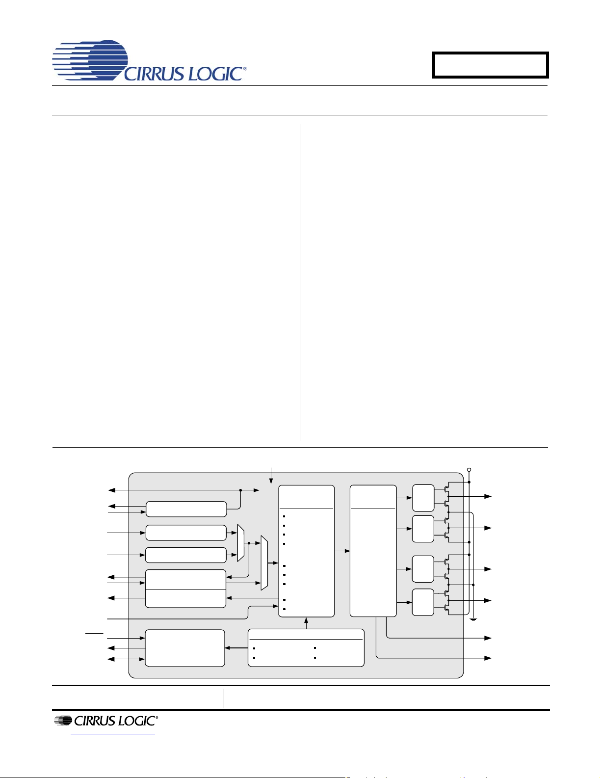
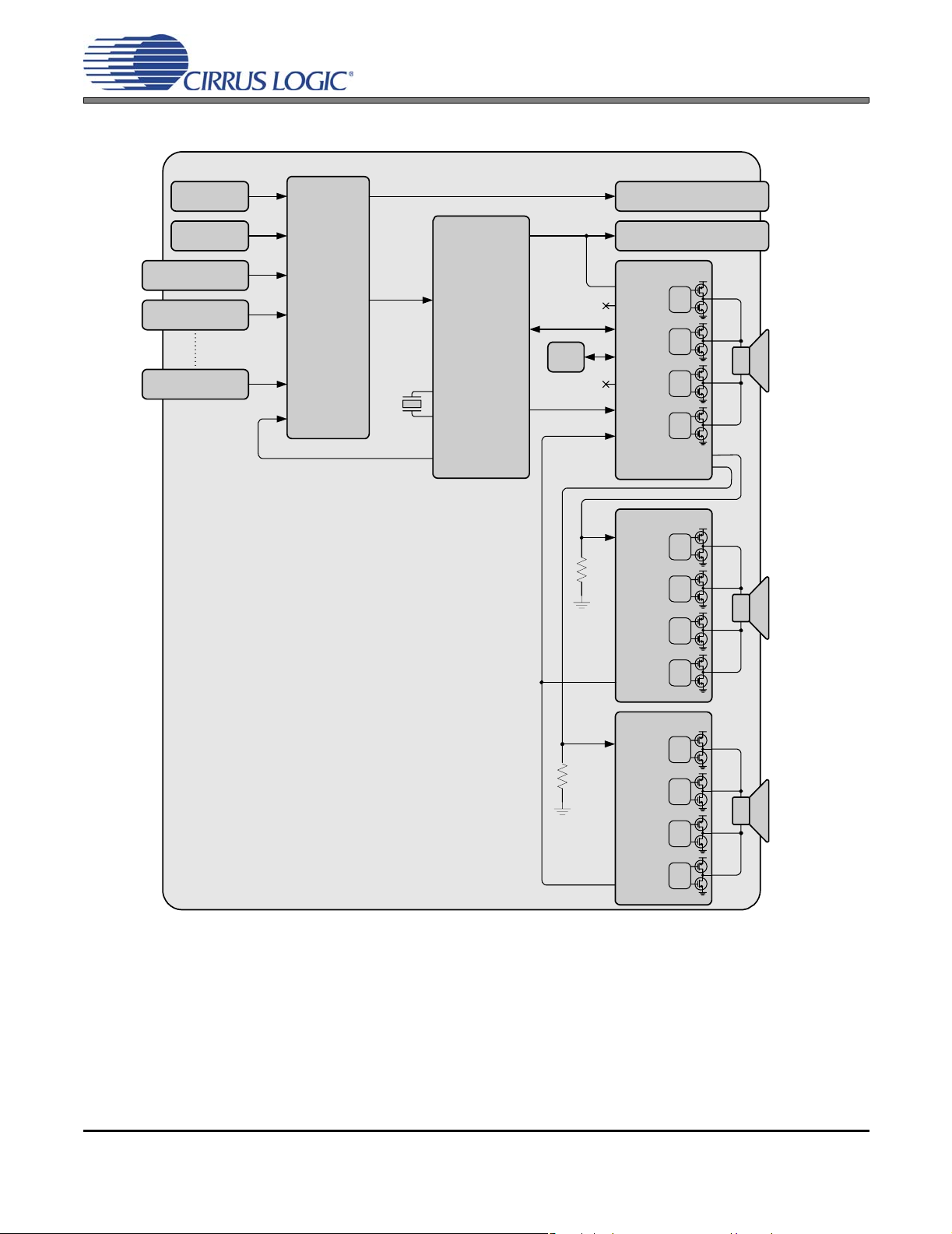
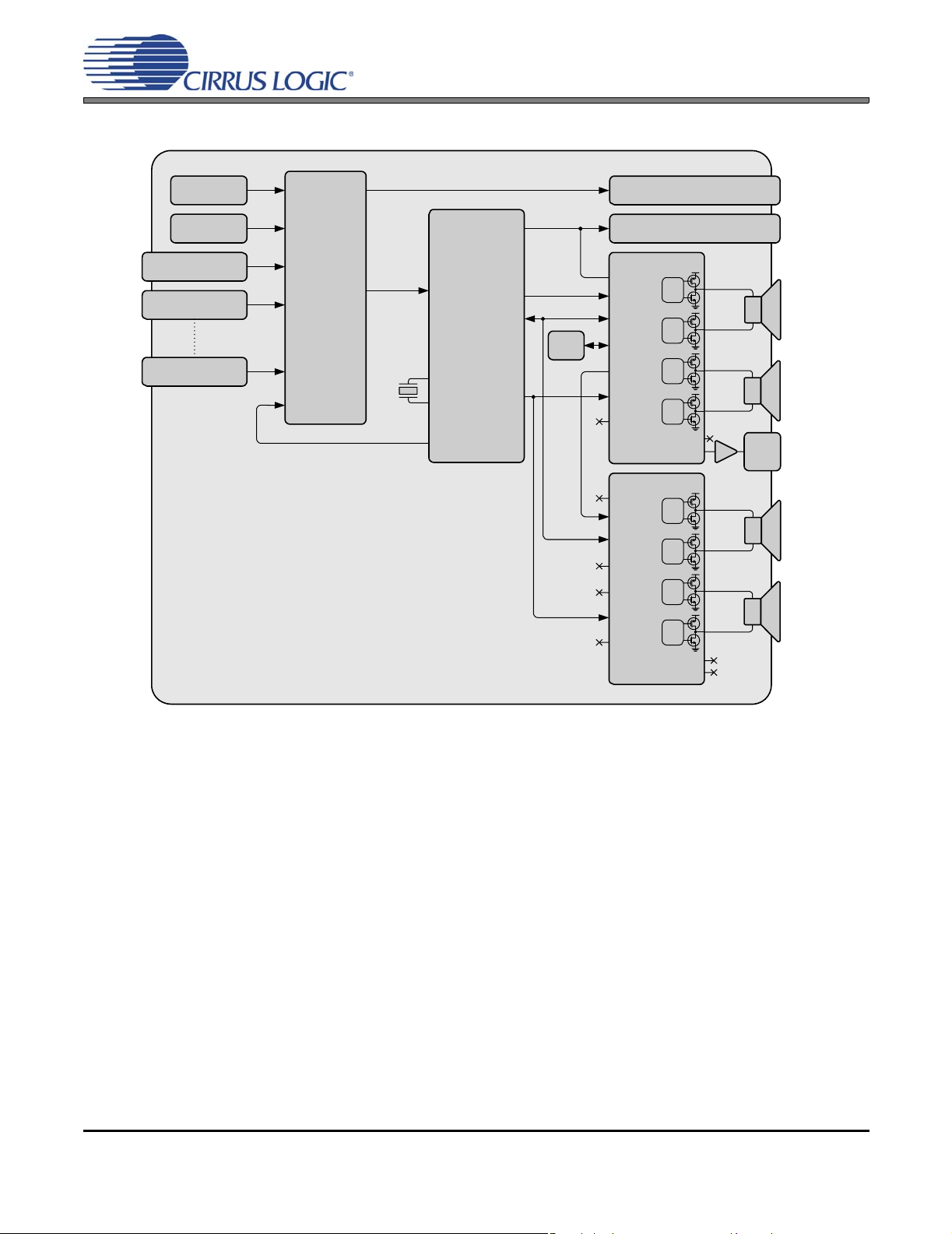
General Description
The CS4525 is a stereo analog or digital input PWM
high efficiency Class D amplifier audio system with an
integrated stereo analog-to-digital (A/D) converter. The
stereo power amplifiers can deliver up to 15 W per
channel into 8 Ω speakers from a small space-saving
48-pin QFN package. The PWM amplifier can achieve
greater than 85% efficiency. The package is thermally
enhanced for optimal heat dis sipation which eliminat es
the need for a heatsink.
The power stage outputs can be con fig ur ed as t w o fu llbridge channels for 2 x 15 W operation, two half-bridge
channels and one full-bridge channel for
2 x 7 W + 1 x 15 W operation, or one parallel full-bridge
channel for 1 x 30 W operation. The CS4525 integrates
on-chip over-current, under-voltage, and over-temperature protection and error reporting as well as a thermal
warning indicator and programmable foldback of the
output power to allow cooling.
The main digital serial port on the CS4525 can support
asynchronous operation with the integrated on-chip
sample rate converter (SRC) which eases system integration. The SRC allows for a fixed PWM switching
frequency regardless of incoming sample rate as well
as optimal clocking for the A/D modulators.
An on-chip oscillator driver eliminates the need for an
external crystal oscillator circuit, reducing overall design
cost and conserving circuit board space. The CS4525
automatically uses the on-chip oscillator driver in the
absence of an applied master clock.
The CS4525 is available in a 48-pin QFN package in
Commercial grade (-10° to +70° C). The CRD4525-Q1
4-layer, 1 oz. copper and CRD4525-D1 2-layer, 1 oz.
copper customer reference designs are also available.
Please refer to “Ordering Information” on page 97 for
complete ordering information.
2 DS726PP2
Page 3

TABLE OF CONTENTS
1. PIN DESCRIPTIONS - SOFTWARE MODE .......................................................................................... 8
2. PIN DESCRIPTIONS - HARDWARE MODE ....................................................................................... 10
2.1 Digital I/O Pin Characteristics ........ ... ... ... .... ... ... ... .......................................... .... ... ... ... ... ................ 12
3. TYPICAL CONNECTION DIAGRAMS .................................................................................................13
4. TYPICAL SYSTEM CONFIGURATION DIAGRAMS ........................................................................... 15
5. CHARACTERISTICS AND SPECIFICATIONS .................................................................................... 18
6. APPLICATIONS ................................................................................................................................... 26
6.1 Software Mode .................................. ... ... .... ... ... ... .... .......................................... ... ... ... ................... 26
6.1.1 System Clocking ................................................................................................................... 26
6.1.1.1 SYS_CLK Input Clock Mode .................................................................................... 26
6.1.1.2 Crystal Oscillator Mode ............................................................................................ 27
6.1.2 Power-Up and Power-Down .................................................................................................28
6.1.2.1 Recommended Power-Up Sequence ....................................................................... 28
6.1.2.2 Recommended Power-Down Sequence .................................................................. 28
6.1.3 Input Source Selection .......................................................................................................... 29
6.1.4 Digital Sound Processing ...................................................................................................... 29
6.1.4.1 Pre-Scaler ................................................................................................................. 30
6.1.4.2 Digital Signal Processing High-Pass Filter ............................................................... 30
6.1.4.3 Channel Mixer ..........................................................................................................30
6.1.4.4 De-Emphasis ............................................................................................................31
6.1.4.5 Tone Control ............................................................................................................. 31
6.1.4.6 Parametric EQ ..........................................................................................................33
6.1.4.7 Adaptive Loudness Compensation .............................. ............................................. 34
6.1.4.8 Bass Management .................................................................................................... 35
6.1.4.9 Volume and Muting Control ...................................................................................... 36
6.1.4.10 Peak Signal Limiter .............. ... ... ... .... ... ... ... .... ... ... ... .......................................... ... ... 37
6.1.4.11 Thermal Limiter ................ .... ... ... .......................................... ... .... ... ... ... ... .... ... ... ... ...39
6.1.4.12 Thermal Foldback ......................... .... ... ... ... .... ... ... ... .......................................... ... ... 40
6.1.4.13 2-Way Crossover & Sensitivity Control .......... ......................... .......................... ...... 41
6.1.5 Auxiliary Serial Output .......................................................................................................... 43
6.1.6 Serial Audio Delay & Warning Input Port .............................................................................. 44
6.1.6.1 Serial Audio Delay Interface ..................................................................................... 44
6.1.6.2 External Warning Input Port ..................................................................................... 44
6.1.7 Powered PWM Outputs ........................................................................................................ 45
6.1.7.1 Output Channel Configurations ................................................................................ 45
6.1.7.2 PWM Popguard Transient Control ............................................................................ 45
6.1.8 Logic-Level PWM Outputs .................................................................................................... 46
6.1.8.1 Recommended PWM_SIG Power-Up Sequence for an External PWM Amplifier .... 47
6.1.8.2 Recommended PWM_SIG Power-Down Sequence for an External PWM Amplifier 47
6.1.8.3 Recommended PWM_SIG Power-Up Sequence for Headphone & Line-Out .......... 48
6.1.8.4 Recommended PWM_SIG Power-Down Sequence for Headphone & Line-Out ..... 48
6.1.8.5 PWM_SIG Logic-Level Output Configurations ......................................................... 49
6.1.9 PWM Modulator Configuration .................... .... ... ... ............................................. ...................50
6.1.9.1 PWM Channel Delay ................................................................................................ 50
6.1.9.2 PWM AM Frequency Shift ........................................................................................ 51
6.1.10 Headphone Detection & Hardware Mute Input ................................................................... 51
6.1.11 Interrupt Reporting .............................................................................................................. 53
6.1.12 Automatic Power Stage Shut-Down ................................................................................... 53
6.2 Hardware Mode .......................... ... ... ... ... .... .......................................... ... ... ... .... ... ... ...................... 54
6.2.1 System Clocking ................................................................................................................... 54
6.2.2 Power-Up and Power-Down .................................................................................................54
6.2.2.1 Recommended Power-Up Sequence ....................................................................... 54
CS4525
DS726PP2 3
Page 4

CS4525
6.2.2.2 Recommended Power-Down Sequence ............ ... ... ... .... ... ... ... .... ... ... ... ... ................ 55
6.2.3 Input Source Selection .......................... ... ... .... ... ... ... .... ... ... ... ... .... ... ... ... .... ............................ 55
6.2.4 PWM Channel Delay ............................................................................................................ 55
6.2.5 Digital Signal Flow ................................................................................................................ 56
6.2.5.1 High-Pass Filter ........................................................................................................ 56
6.2.5.2 Mute Control ............................................................................................................. 56
6.2.5.3 Warning and Error Reporting .................................................................................... 56
6.2.6 Thermal Foldback ................................................................................................................. 57
6.2.7 Automatic Power Stage Shut-Down ..................................................................................... 58
6.3 PWM Modulators and Sample Rate Converters ............................................................................ 58
6.4 Output Filters ................................................................................................................................. 59
6.4.1 Half-Bridge Output Filter ....................................................................................................... 59
6.4.2 Full-Bridge Output Filter (Stereo or Parallel) ........................................................................ 60
6.5 Analog Inputs ................................................................................................................................. 61
6.6 Serial Audio Interfaces ................................................................................................................... 62
6.6.1 I²S Data Format .................................................................................................................... 62
6.6.2 Left-Justified Data Format .................................................................................................... 62
6.6.3 Right-Justified Data Format .................................................................................................. 63
6.7 Integrated VD Regulator ................................................................................................................ 63
6.8 I²C Control Port Description and Timing ........................................................................................ 64
7. PCB LAYOUT CONSIDERATIONS ..................................................................................................... 65
7.1 Power Supply, Grounding .............................................................................................................. 65
7.2 QFN Thermal Pad .......................................................................................................................... 65
8. REGISTER QUICK REFERENCE ........................................................................................................ 66
9. REGISTER DESCRIPTIONS ................................................................................................................ 69
9.1 Clock Configuration (Address 01h) ................................................................................................ 69
9.1.1 SYS_CLK Output Enable (EnSysClk) ................................................................................... 69
9.1.2 SYS_CLK Output Divider (DivSysClk) .................................................................................. 69
9.1.3 Clock Frequency (ClkFreq[1:0]) ............................................................................................ 69
9.1.4 HP_Detect/Mute Pin Active Logic Level (HP/MutePol) ...................... ................... ................ 70
9.1.5 HP_Detect/Mute Pin Mode (HP/Mute) .................................................................................. 70
9.1.6 Modulator Phase Shifting (PhaseShift) ................................. ............................................. ... 70
9.1.7 AM Frequency Shifting (FreqShift) ....................................................................................... 70
9.2 Input Configuration (Address 02h) ................................................................................................. 71
9.2.1 Input Source Selection (ADC/SP) ................................... ... ... ... .... ... ... ... .... ... ... ... ... .... ... ......... 71
9.2.2 ADC High-Pass Filter Enable (EnAnHPF) ................................... ... ... ... .... ... ... ... ... .... ... ... ... ... 71
9.2.3 Serial Port Sample Rate (SPRate[1:0]) - Read Only ................................ ... ... ... ... .... ... ... ... ... 71
9.2.4 Input Serial Port Digital Interface Format (DIF [2:0]) ............................................................ 71
9.3 AUX Port Configuration (Address 03h) .......................................................................................... 72
9.3.1 Enable Aux Serial Port (EnAuxPort) ..................................................................................... 72
9.3.2 Delay & Warning Port Configuration (DlyPortCfg[1:0]) ......................................................... 72
9.3.3 Aux/Delay Serial Port Digital Interface Format (AuxI²S/LJ) ............... ... .... ... ... ... ....... ... ... ... ... 72
9.3.4 Aux Serial Port Right Channel Data Select (RChDSel[1:0]) ................................................. 72
9.3.5 Aux Serial Port Left Channel Data Select (LChDSel[1:0]) .................................................... 73
9.4 Output Configuration (Address 04h) ............................................................................................. 73
9.4.1 Output Configuration (OutputCfg[1:0]) .................................................................................. 7
9.4.2 PWM Signals Output Data Select (PWMDSel[1:0]) ........................ ...................................... 73
9.4.3 Channel Delay Settings (OutputDly[3:0]) .............................................................................. 73
9.5 Foldback and Ramp Configuration (Address 05h) ......................................................................... 74
9.5.1 Select VP Level (SelectVP) .................................................................................................. 74
9.5.2 Enable Thermal Foldback (EnTherm) ................................................................................... 74
9.5.3 Lock Foldback Adjust (LockAdj) ...........................................................................................74
9.5.4 Foldback Attack Delay (AttackDly[1:0]) ................................................................................ 75
9.5.5 Enable Foldback Floor (EnFloor) .......................... ............................................. ...................75
3
4 DS726PP2
Page 5

CS4525
9.5.6 Ramp Speed (RmpSpd[1:0]) ................................................................................................ 75
9.6 Mixer / Pre-Scale Configuration (Address 06h) ............................................................................. 75
9.6.1 Pre-Scale Attenuation (PreScale[2:0]) .................................................................................. 75
9.6.2 Right Channel Mixer (RChMix[1:0]) ...................................................................................... 76
9.6.3 Left Channel Mixer (LChMix[1:0]) .........................................................................................76
9.7 Tone Configuration (Address 07h) ................................. ... .... ... ... ... ... .... ... ... ... .... ... ... ... ... .... ... ......... 76
9.7.1 De-Emphasis Control (DeEmph) .......................................................................................... 76
9.7.2 Adaptive Loudness Compensation Control (Loudness) ....................................................... 76
9.7.3 Digital Signal Processing High-Pass Filter (EnDigHPF) ....................................................... 77
9.7.4 Treble Corner Frequency (TrebFc[1:0]) ....................... ................................................ ......... 77
9.7.5 Bass Corner Frequency (BassFc[1:0]) ................................................................................. 77
9.7.6 Tone Control Enable (EnToneCtrl) ....................................................................................... 77
9.8 Tone Control (Address 08h) ........................ ... ... ... .... ... ... ... .......................................... ... .... ............ 78
9.8.1 Treble Gain Level (Treb[3:0]) ................................................................................................78
9.8.2 Bass Gain Level (Bass[3:0]) ................................................................................................. 78
9.9 2.1 Bass Manager/Parametric EQ Control (Address 09h) ............................................................. 78
9.9.1 Freeze Controls (Freeze) ................................ ............. ................ ................ ................ ......... 78
9.9.2 Hi-Z PWM_SIG Outputs (HiZPSig) ....................................................................................... 79
9.9.3 Bass Cross-Over Frequency (BassMgr[2:0]) ........................................................................ 79
9.9.4 Enable Channel B Parametric EQ (EnChBPEq) ................................................................... 79
9.9.5 Enable Channel A Parametric EQ (EnChAPEq) ................................................................... 79
9.10 Volume and 2-Way Cross-Over Configuration (Address 55h) .................................. ... .... ... ... ... ... 80
9.10.1 Soft Ramp and Zero Cross Control (SZCMode[1:0]) .......................................................... 80
9.10.2 Enable 50% Duty Cycle for Mute Condition (Mute50/50) ................................................... 80
9.10.3 Auto-Mute (AutoMute) ........................................................................................................ 80
9.10.4 Enable 2-Way Crossover (En2Way) ...................... .... ... ... ... .......................................... ... ... 81
9.10.5 2-Way Cross-Over Frequency (2WayFreq[2:0]) ................................................................. 81
9.11 Channel A & B: 2-Way Sensitivity Control (Address 56h) ............................................................ 81
9.11.1 Channel A and Channel B Low-Pass Sensitivity Adjust (LowPass[3:0]) ............................ 81
9.11.2 Channel A and Channel B High-Pass Sensitivity Adjust (HighPass[3:0]) ........................... 82
9.12 Master Volume Control (Address 57h) ............................... ... ... ... ... .... ......................................... 82
9.12.1 Master Volume Control (MVol[7:0]) .................................................................................... 82
9.13 Channel A and B Volume Control (Address 58h & 59h) ........................... ... .... ... ... ... ... .... ............ 83
9.13.1 Channel X Volume Control (ChXVol[7:0]) ........................................................................... 83
9.14 Sub Channel Volume Control (Address 5Ah) ........ ... ... ... .... ... ... ... .......................................... ... ... 83
9.14.1 Sub Channel Volume Control (SubVol[7:0]) ....................................................................... 83
9.15 Mute/Invert Control (Address 5Bh) .............................................................................................. 84
9.15.1 ADC Invert Signal Polarity (InvADC) .................................................................................. 84
9.15.2 Invert Channel PWM Signal Polarity (InvChX) ................................................................... 84
9.15.3 Invert Sub PWM Signal Polarity (InvSub) ........................................................................... 84
9.15.4 ADC Channel Mute (MuteADC) .......................................................................................... 84
9.15.5 Independent Channel A & B Mute (MuteChX) .................................................................... 84
9.15.6 Sub Channel Mute (MuteSub) ............................................................................................ 85
9.16 Limiter Configuration 1 (Address 5Ch) ......................................................................................... 85
9.16.1 Maximum Threshold (Max[2:0]) .......................................................................................... 85
9.16.2 Minimum Threshold (Min[2:0]) ............................................ ... .............................................85
9.16.3 Peak Signal Limit All Channels (LimitAll) ............................................................................ 86
9.16.4 Peak Detect and Limiter Enable (EnLimiter) ....................... .................... ................... ......... 86
9.17 Limiter Configuration 2 (Address 5Dh) ......................................................................................... 87
9.17.1 Limiter Release Rate (RRate[5:0]) ...................................... ................ ................ ................ 87
9.18 Limiter Configuration 3 (Address 5Eh) ......................................................................................... 87
9.18.1 Enable Thermal Limiter (EnThLim) ..................................................................................... 87
9.18.2 Limiter Attack Rate (ARate[5:0]) ......................................................................................... 87
9.19 Power Control (Address 5Fh) ......................................................... .... ... ...................................... 88
DS726PP2 5
Page 6

CS4525
9.19.1 Automatic Power Stage Retry (AutoRetry) ......................................................................... 88
9.19.2 Enable Over-Current Protection (EnOCProt) ...................................................................... 88
9.19.3 Select VD Level (SelectVD) ................................................................................................ 88
9.19.4 Power Down ADC (PDnADC) ............................................................................................. 88
9.19.5 Power Down PWM Power Output X (PDnOutX) ........................ ................ ................ ......... 88
9.19.6 Power Down (PDnAll) ......................................................................................................... 89
9.20 Interrupt (Address 60h) ............................ ................................................................................... 89
9.20.1 SRC Lock State Transition Interrupt (SRCLock) ................................................................ 89
9.20.2 ADC Overflow Interrupt (ADCOvfl) ..................................................................................... 90
9.20.3 Channel Overflow Interrupt (ChOvfl) .................................................................................. 90
9.20.4 Amplifier Error Interrupt Bit (AmpErr) ..................................................................................90
9.20.5 Mask for SRC State (SRCLockM) ...................................................................................... 91
9.20.6 Mask for ADC Overflow (ADCOvflM) .................................................................................. 91
9.20.7 Mask for Channel X and Sub Overflow (ChOvflM) ............................................................. 91
9.20.8 Mask for Amplifier Error (AmpErrM) ................................................................................... 92
9.21 Interrupt Status (Address 61h) - Read Only ................................................................................. 92
9.21.1 SRC State Transition (SRCLockSt) .................................................................................... 92
9.21.2 ADC Overflow (ADCOvflSt) ................................................................................................92
9.21.3 Sub Overflow (SubOvflSt) ................................................................................................... 92
9.21.4 Channel X Overflow (ChXOvflSt) ........................................................................................ 93
9.21.5 Ramp-Up Cycle Complete (RampDone) ............................................................................ 93
9.22 Amplifier Error Status (Address 62h) - Read Only ....................................................................... 93
9.22.1 Over-Current Detected On Channel X (OverCurrX) ........... ... .... ... ... ... .... ... ... ... ... .... ... ... ... ... 93
9.22.2 External Amplifier State (ExtAmpSt) ................................................................................... 93
9.22.3 Under Voltage / Thermal Error State (UVTE[1:0]) .............................................................. 94
9.23 Device I.D. and Revision (Address 63h) - Read Only .................................................................. 94
9.23.1 Device Identification (DeviceID[4:0]) ...................................................................................94
9.23.2 Device Revision (RevID[2:0]) .............................................................................................. 94
10. PARAMETER DEFINITIONS .............................................................................................................. 95
11. REFERENCES .................................................................................................................................... 95
12. PACKAGE DIMENSIONS .................................................................................................................. 96
13. THERMAL CHARACTERISTICS ....................................................................................................... 97
13.1 Thermal Flag ... ... ... ... .......................................... .... ... ... ... .... ... ... ... ... .... ......................................... 97
14. ORDERING INFORMATION .............................................................................................................. 97
15. REVISION HISTORY .......................................................................................................................... 98
LIST OF FIGURES
Figure 1.Typical Connection Diagram - Software Mode ........................................................................... 13
Figure 2.Typical Connection Diagram - Hardware Mode .................... ...................................................... 14
Figure 3.Typical System Configuration 1 .................................................................................................. 15
Figure 4.Typical System Configuration 2 .................................................................................................. 15
Figure 5.Typical System Configuration 3 .................................................................................................. 16
Figure 6.Typical System Configuration 4 .................................................................................................. 17
Figure 7.Serial Audio Input Port Timing ................. ... ... ... .... ... ... ... .... ... ... ... ... .... ... ... ... .... ... ... ... ... ................ 21
Figure 8.AUX Serial Port Interface Master Mode Timing .......................................................... ................22
Figure 9.SYS_CLK Timing from Reset ..................................................................................................... 23
Figure 10.PWM_SIGX Timing ................................... ... ... .... ... ... ... .... ... ... ... ... .... ... ... ... .... ............................ 23
Figure 11.Control Port Timing - I²C ........................................................................................................... 24
Figure 12.Typical SYS_CLK Input Clocking Configuration .......................................................................26
Figure 13.Typical Crystal Oscillator Clocking Configuration ..................................................................... 27
Figure 14.Digital Signal Flow .................................................................................................................... 29
Figure 15.De-Emphasis Filter ............................ .... ... ... ... .... ... ... ... .... ... ... ................................................... 31
Figure 16.Bi-Quad Filter Architecture .............................. .......... .......... ...... .......... .......... ......... ................... 33
6 DS726PP2
Page 7

Figure 17.Peak Signal Detection & Limiting .............................................................................................. 37
Figure 18.Foldback Process ..................................................................................................................... 40
Figure 19.Popguard Connection Diagram ................................................................................................. 46
Figure 20.2-Channel Full-Bridge PWM Output Delay ...............................................................................50
Figure 21.3-Channel PWM Output Delay .................................................................................................. 50
Figure 22.Typical SYS_CLK Input Clocking Configuration .... ................ ................................................... 54
Figure 23.Hardware Mode PWM Output Delay ......................................................................................... 55
Figure 24.Hardware Mode Digital Signal Flow .......................................................................................... 56
Figure 25.Foldback Process ..................................................................................................................... 57
Figure 26.Output Filter - Half-Bridge ......................................................................................................... 59
Figure 27.Output Filter - Full-Bridge .......................................................................................................... 60
Figure 28.Recommended Unity Gain Input Filter ...................................................................................... 61
Figure 29.Recommended 2 V
Figure 30.I²S Serial Audio Formats ........................................................................................................... 62
Figure 31.Left-Justified Serial Audio Formats ........................................................................................... 62
Figure 32.Right-Justified Serial Audio Formats ................... ... ... ... .... ... ... ... ................................................ 63
Figure 33.Control Port Timing, I²C Write ................................................................................................... 64
Figure 34.Control Port Timing, I²C Read ................................................................................................... 64
LIST OF TABLES
Table 1. I/O Power Rails ........................................................................................................................... 12
Table 2. Bass Shelving Filter Corner Frequencies ....................... .......................................... ... .... ... ......... 31
Table 3. Treble Shelving Filter Corner Frequencies ................................................................................. 32
Table 4. Bass Management Cross-Over Frequencies ..................................... ... ... ... .... ... ... ... ... .... ............ 35
Table 5. 2-Way Cross-Over Frequencies .................................................................................................. 41
Table 6. Auxiliary Serial Port Data Output .......................... ... ... ... .... ... ...................................................... 43
Table 7. Nominal Switching Frequencies of the Auxiliary Serial Output ................................................... 43
Table 8. PWM Power Output Configurations ............................................................................................ 45
Table 9. Typical Ramp Times for Various VP Voltages ............................................................................46
Table 10. PWM Logic-Level Output Configurations .................................................................................. 49
Table 11. PWM Output Switching Rates and Quantization Levels ..................................... ... ... .... ... ... ... ... 51
Table 12. Output of PWM_SIG Outputs .................................................................................................... 52
Table 13. SYS_CLOCK Frequency Selection ........................................................................................... 54
Table 14. Input Source Selection .................................... .......................................................................... 55
Table 15. Serial Audio Interface Format Selection .................................................................................... 55
Table 16. Thermal Foldback Enable Selection ...................... ... ... .... ... ... ... ... .... ......................................... 57
Table 17. PWM Output Switching Rates and Quantization Levels ..................................... ... ... .... ... ... ... ... 58
Table 18. Low-Pass Filter Components - Half-Bridge ............................................................................... 59
Table 19. DC-Blocking Capacitors Values - Half-Bridge .............................. ............................................. 59
Table 20. Low-Pass Filter Components - Full-Bridge ............................................................................... 60
Table 21. Power Supply Configuration and Settings ................................................................................. 63
CS4525
Input Filter ........................................................................................... 61
RMS
DS726PP2 7
Page 8
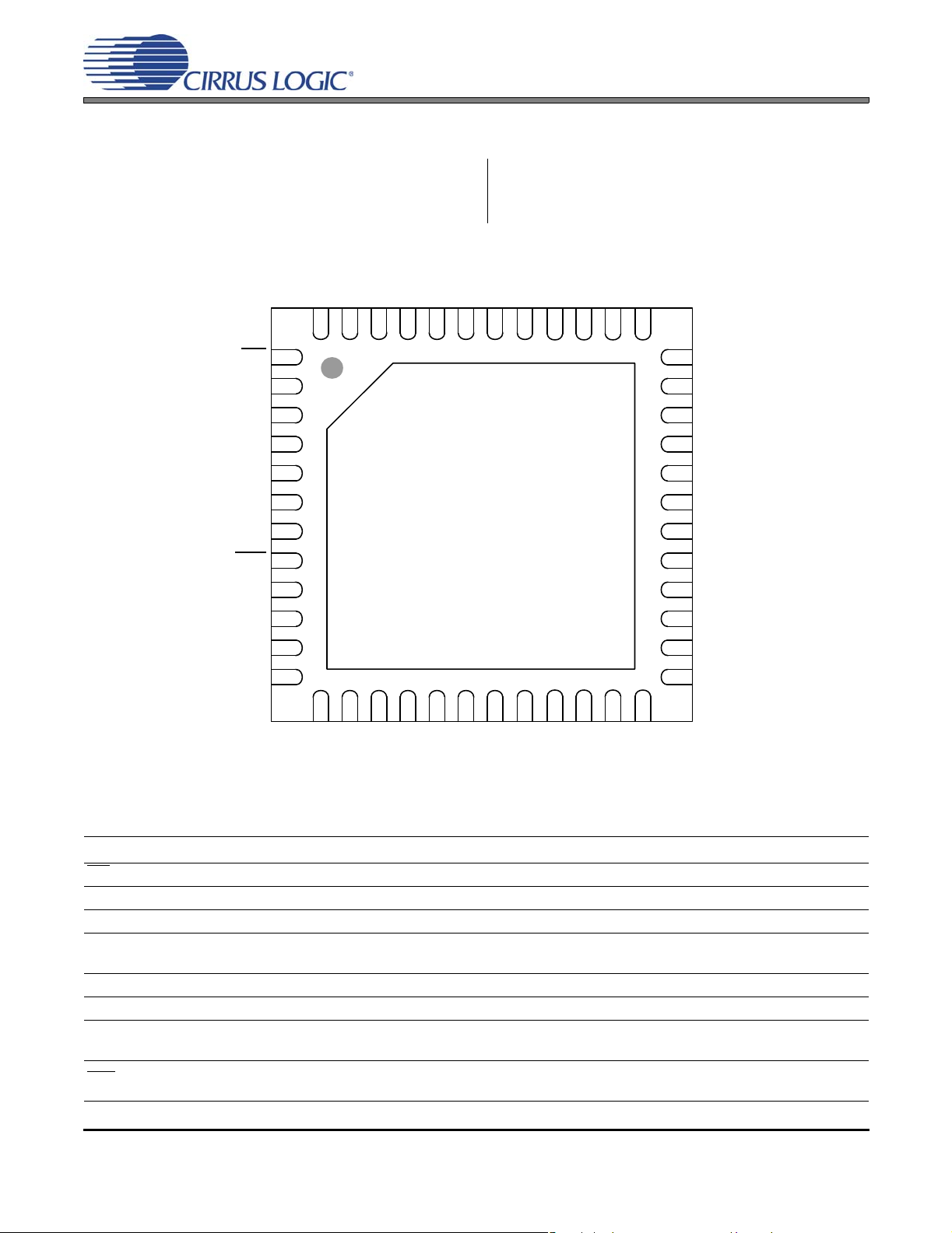
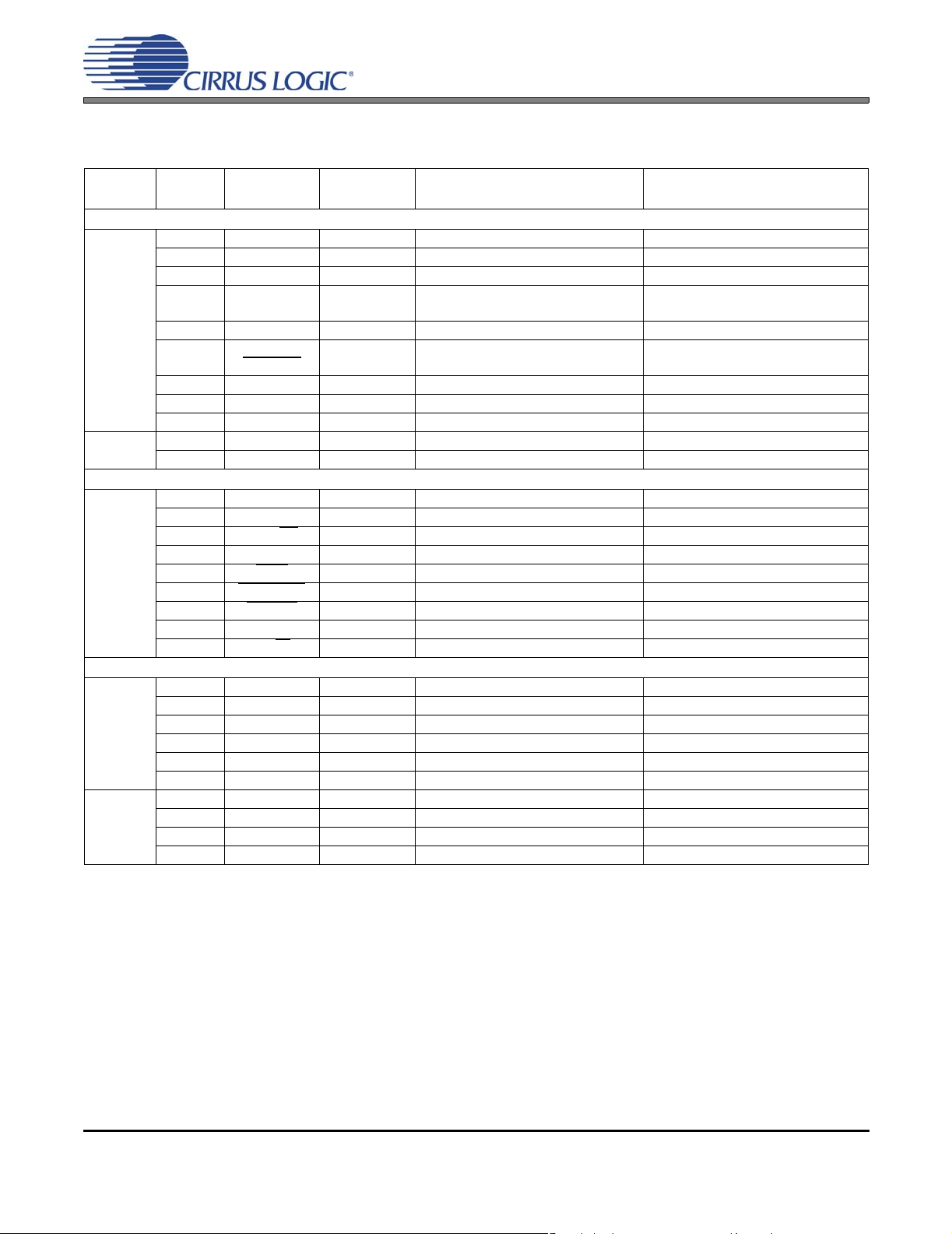
1. PIN DESCRIPTIONS - SOFTWARE MODE
XTI
XTO
SYS_CLK
AUX_LRCK/AD0
AUX_SCLK
AUX_SDOUT
DLY_SDIN/EX_TWR
4748 46
45
44 43 42 41
DLY_SDOUT
PWM_SIG1
PWM_SIG2
40 39 38 37
PGND
PGND
CS4525
INT
SCL
SDA
LRCK
SCLK
SDIN
HP_DETECT/MUTE
RST
LVD
DGND
VD_REG
VD
1
2
3
4
5
6
Thermal Pad
7
8
9
10
11
12
1413 15
AGND
VA_REG
Top-Down (Through Package) View
48-Pin QFN Package
17 18 19 20
16
VQ
FILT+
AFILTL
AINL
AFILTR
21 22 23 24
AINR
OCREF
PGND
PGND
36
35
34
33
32
31
30
29
28
27
26
25
VP
OUT1
PGND
PGND
OUT2
VP
VP
OUT3
PGND
PGND
OUT4
VP
RAMP_CAP
Pin Name Pin # Pin Description
INT 1Interrupt (Output) - Indicates an interrupt condition has occurred.
SCL 2 Serial Control Port Clock (Input) - Serial clock for the I²C control port.
SDA 3 Serial Control Data (Input/Output) - Bi-directional data I/O for the I²C control port.
LRCK 4
Left Right Clock (Input) - Determines which channel, Left or Right, is currently active on the serial
audio data line.
SCLK 5 Serial Clock (Input) - Serial bit clock for the serial audio interface.
SDIN 6 Serial Audio Data Input (Input) - Input for two’s complement serial audio data.
HP_DETECT/
MUTE
8
RST
Headphone Detect / Mute (Input) - Headphone detection or mute input signal as configured via the
7
I²C control port.
Reset (Input) - The device enters a low power mode and all internal registers are reset to their
default settings when this pin is driven low.
8 DS726PP2
Page 9

CS4525
VD Voltage Level Indicator (Input) - Identifies the voltage level attached to VD. When applying
LVD 9
DGND 10 Digital Ground (Input) - Ground for the internal logic and digital I/O.
VD_REG 11 Core Logic Power (Output) - Internally generated low voltage power supply for digital logic.
VD 12 Power (Input) - Positive power supply for the internal regulators and digital I/O.
VA_REG 13 Analog Power (Output) - Internally generated positive power for the analog section and I/O.
AGND 14 Analog Ground (Input) - Ground reference for the internal analog section and I/O.
FILT+ 15
VQ 16 Common Mode Voltage (Output) - Filter connection for internal common mode voltage.
AFILTL
AFILTR
AINL
AINR
OCREF 21 Over Current Reference Setting (Input) - Sets the reference for over current detection.
22,23
PGND
RAMP_CAP 24
VP
OUT4
OUT3
OUT2
OUT1
PWM_SIG2
PWM_SIG1
DL Y_SDOUT 41 Delay Serial Audio Data Out (Output) - Output for two’s complement serial audio data.
DL Y_SDIN/
EX_TWR
AUX_SDOUT 43
AUX_SCLK 44 Auxiliary Port Serial Clock (Output) - Serial clock for the auxiliary port serial interface.
AUX_LRCK/
AD0
SYS_CLK 46
XTO 47 Crystal Oscillator Output (Output) - Crystal oscillator driver output.
XTI 48 Crystal Oscillator Input (Input) - Crystal oscillator driver input.
Thermal Pad -
27,28
33,34
37,38
25,30,
31,36
5.0 V to VD, LVD must be connected to VD. When applying 2.5 V or 3.3 V to VD, L VD must be
DGND.
Positive Voltage Reference (Output) - Positive reference voltage for the internal ADC sampling
circuits.
17
Antialias Filter Connection (Output) - Antialias filter connection for ADC inputs.
18
1920Analog Input (Input) - The full-scale input level is specified in the ADC Analog Characteristics
specification table.
Power Ground (Input) - Ground for the individual output power half-bridge devices.
Output Ramp Capacitor (Input) - Used by the PWM Popguard Transient Control to suppress the
initial pop in half-bridge-configured outputs.
High Voltage Power (Input) - High voltage power supply for the individual half-bridge devices.
26
29
PWM Output (Output) - Amplified PWM power outputs.
32
35
39
Logic Level PWM Output (Output) - Logic Level PWM switching signals.
40
Delay Serial Audio Data Input (Input) - Input for two’s complement serial audio data.
42
External Thermal Warning (Input) - Input for an external thermal warning signal. Configurable via
the I²C control port.
Auxiliary Port Serial Audio Data Out (Output) - Output for two’s complement auxiliary port serial
data.
Auxiliary Port Left Right Clock (Output) - Determines which channel, Left or Right, is currently
45
active on the serial audio data line.
AD0 (Input) - Sets the LSB of the I²C device address. Sensed on the release of RST
System Clock (Input/Output) -Clock source for the internal logic, processing, and modulators. This
pin should be connected to through a 10kΩ to ground when unused.
Thermal Pad - Thermal relief pad for optimized heat dissipation. See “QFN Thermal Pad” on
page 65 for more information.
.
DS726PP2 9
Page 10
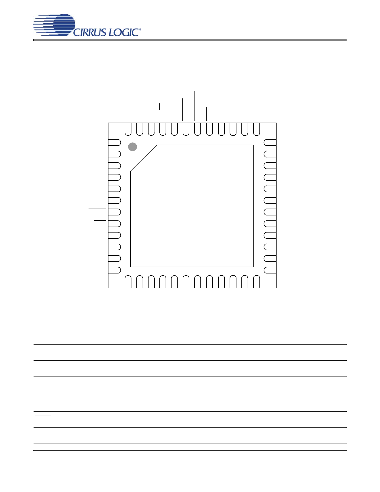
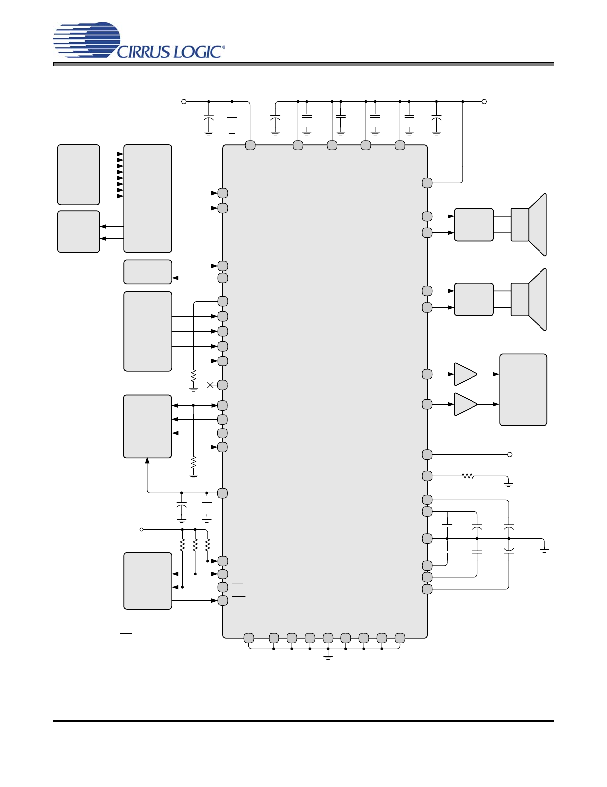
2. PIN DESCRIPTIONS - HARDWARE MODE
EN_TFB
ERROC
TSTI
4748 46
TSTO
SYS_CLK
I2S/LJ
45
44 43 42 41
ERRUVTE
TWR
TSTO
TSTO
40 39 38 37
PGND
PGND
CS4525
CLK_FREQ0
CLK_FREQ1
ADC/SP
LRCK
SCLK
SDIN
MUTE
RST
LVD
DGND
VD_REG
VD
1
2
3
4
5
6
Thermal Pad
7
8
9
10
11
12
1413 15
AGND
VA_REG
Top-Down (Through Package) View
48-Pin QFN Package
17 18 19 20
16
VQ
FILT+
AFILTL
AINL
AFILTR
21 22 23 24
AINR
OCREF
PGND
PGND
36
35
34
33
32
31
30
29
28
27
26
25
VP
OUT1
PGND
PGND
OUT2
VP
VP
OUT3
PGND
PGND
OUT4
VP
RAMP_CAP
Pin Name Pin # Pin Description
CLK_FREQ0
CLK_FREQ1
ADC/SP 3
LRCK 4
SCLK 5 Serial Clock (Input) - Serial bit clock for the serial audio interface.
SDIN 6 Serial Audio Data Input (Input) - Input for two’s complement serial audio data.
7
MUTE
8
RST
12Clock Frequency (Input) - Determines the frequency of the clock expected to be driven into the
SYS_CLK pin.
ADC/Serial Port (Input) - Selects between the Analog to Digital Converter and the Serial Port for
audio input. Selects the ADC when high or the serial port when low.
Left Right Clock (Input) - Determines which channel, Left or Right, is currently active on the serial
audio data line.
Mute (Input) - The PWM outputs will output silence as a 50% duty cycle signa l when this pin is
driven low.
Reset (Input) - The device enters a low power mode and all internal registers are reset to their
default settings when this pin is driven low.
10 DS726PP2
Page 11
CS4525
VD Voltage Level Indicator (Input) - Identifies the voltage level attached to VD. When applying
LVD 9
DGND 10 Digital Ground (Input) - Ground for the internal logic and I/O.
VD_REG 11 Core Logic Power (Output) - Internally generated low voltage power supply for digital logic.
VD 12 Digital Power (Input) - Positive power supply for the internal regulators and digital I/O.
VA_REG 13 Analog Power (Output) - Internally generated positive power for the analog section and I/O.
AGND 14 Analog Ground (Input) - Ground reference for the internal analog section and I/O.
FILT+ 15
VQ 16 Common Mode Voltage (Output) - Filter connection for internal common mode voltage.
AFILTL
AFILTR
AINL
AINR
OCREF 21 Over Current Reference Setting (Input) - Sets the reference for over current detection.
22,23
PGND
RAMP_CAP 24 Output Ramp Capacitor (Input) - This pin should be connected directly to VP in hardware mode.
VP
OUT4
OUT3
OUT2
OUT1
TSTO
41 Thermal Warning Output (Output) - Thermal warning output.
TWR
ERRUVTE 42
ERROC
EN_TFB 44 Enable Thermal Feedback (Input) - Enables the thermal foldback feature when high.
I2S/LJ
SYS_CLK 46 System Clock (Input/Output) -Clock source for the delta-sigma modulators.
TSTO 47
TSTI 48
Thermal Pad -
43 Overcurrent Error Output (Output) - Overcurrent error flag.
27,28
33,34
37,38
25,30,
31,36
5.0 V to VD, LVD must be connected to VD. When applying 2.5 V or 3.3 V to VD, LVD must be connected to DGND.
Positive Voltage Reference (Output) - Positive reference voltage for the internal ADC sampling
circuits.
17
Antialias Filter Connection (Output) - Antialias filter connection for ADC inputs.
18
1920Analog Input (Input) - The full-scale input level is specified in the ADC Analog Characteristics
specification table.
Power Ground (Input) - Ground for the individual output power half-bridge devices.
High Voltage Power (Input) - High voltage power supply for the individual half-bridge devices.
26
29
PWM Output (Output) - Amplified PWM power outputs.
32
35
3940Test Output (Output) - These pins are outputs used for the Logic Level PWM switching signals
available only in software mode. They must be left unconnected for hardware mode operation.
Thermal and Undervoltage Error Outp ut (Output) - Error flag for thermal shutdown and under-
voltage.
I²S/Left Justified (Input) - Selects between I²S and Left-Justified data format for the serial input
45
port. Selects I²S when high and LJ when low.
Test Output (Output) - This pin is an output used for the crystal oscillator driver available only in
software mode. It must be left unconnected for normal hardware mode operation.
Test Input (Input) - This pin is an input used for the crystal oscillator driver available only in soft-
ware mode. It must be tied to digital ground for normal hardware mode operation.
Thermal Pad - Thermal relief pad for optimized heat dissipation. See “QFN Thermal Pad” on
page 65 for more information.
DS726PP2 11
Page 12
CS4525
2.1 Digital I/O Pin Characteristics
The logic level for each input is set by its corresponding power su pply and should not exceed the maximum ratings.
Power
Supply
Pin
Number
Pin Name I/O Driver Receiver
Software Mode
VD 1 INT Output 2.5 V-5.0 V, Open Drain
2 SCL Input - 2.5 V-5.0 V, with Hysteresis
3 SDA Input/Output 2.5 V-5.0 V, Open Drain 2.5 V-5.0 V, with Hysteresis
7HP_DETECT
MUTE
41 DLY_SDOUT Output 2.5 V-5.0V, CMOS 42 DLY_SDIN
EX_TWR
43 AUX_SDOUT Output 2.5 V-5.0V, CMOS 44 AUX_SCLK Output 2.5 V-5.0 V, CMOS 45 AUX_LRCK Output 2.5 V-5.0 V, CMOS -
VD_REG 39 PWM_SIG2 Output 2.5 V, CMOS -
40 PWM_SIG1 Output 2.5 V, CMOS -
Input
Input
Input
Input
-
-
-
-
2.5 V-5.0 V
2.5 V-5.0 V
2.5 V-5.0 V
2.5 V-5.0 V
Hardware Mode
VD 1 SEL_OSC0 Input - 2.5 V-5.0 V
2 SEL_OSC1 Input - 2.5 V-5.0 V
3 ADC/SP
7 MUTE Input - 2.5 V-5.0 V
41 TWR
42 ERRUVTE
43 ERROC
44 EN_TFB Input - 2.5 V-5.0 V
45 I²S/LJ
Input - 2.5 V-5.0 V
Output 2.5 V-5.0 V, Open Drain Output 2.5 V-5.0 V, Open Drain Output 2.5 V-5.0 V, Open Drain -
Input - 2.5 V-5.0 V
All Modes
VD 4 LRCK Input - 2.5 V-5.0 V
5 SCLK Input - 2.5 V-5.0 V
6 SDIN Input - 2.5 V-5.0 V
8 RST Input - 2.5 V-5.0 V
9 LVD Input - 2.5 V-5.0 V
46 SYS_CLK Input/Output 2.5 V-5.0 V, CMOS 2.5 V-5.0 V
VP 26 OUT4 Output 8.0 V-18.0 V Power MOSFET -
29 OUT3 Output 8.0 V-18.0 V Power MOSFET 32 OUT2 Output 8.0 V-18.0 V Power MOSFET 35 OUT1 Output 8.0 V-18.0 V Power MOSFET -
Table 1. I/O Power Rails
12 DS726PP2
Page 13
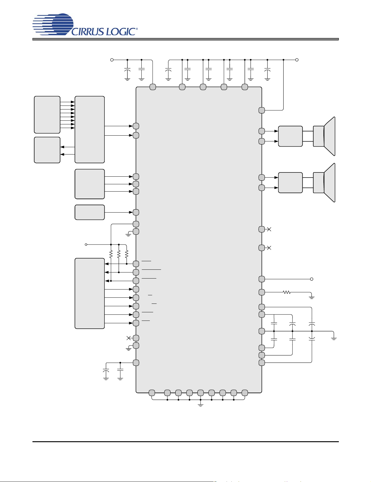
3. TYPICAL CONNECTION DIAGRAMS
CS4525
+3.3 or +5 V
Analog
Audio
Inputs
Analog
Audio
Switch
Analog
Monitor
Output
Crystal
24.576 MHz
MPEG
Audio
Processor
- or -
HDMI
Receiver
Lip-Synch
Delay
NJU26902
+2.5V
0.1 µF
10 µF
VD
22 kΩ
Micro-
Controller
*Note: Resistors are required for I²C control port
operation.
†
Note: On release of RST, AD0 is read as input on the
AUX_LRCK line.
0.1 µF10 µF
12
V
19
AINL
20
AINR
48
XTI
47
XTO
46
SYS_CLK
SCLK5
4
LRCK
6
SDIN
7
HP_DETECT/MUTE
22 kΩ
43
AUX_SDOUT
45
AUX_LRCK/AD0
44
AUX_SCLK
41
DLY_SDOUT
42
†
DLY_SDIN
22 kΩ
11
VD_REG
*
*
2 kΩ
2 kΩ
2
SCL
3
SDA
1
INT
8
RST
10 2322 28 33 34 37 3827
470 µF 0.1 µF 0.1 µF 0.1 µF 0.1 µF 470 µF
313025
D
VP
VP
VP
RAMP_CAP
CS4525
PWM_SIG1
PWM_SIG2
VA_REG
ND
G
D
ND
ND
G
G
P
P
D
ND
N
ND
G
P
G
G
P
P
ND
ND
G
G
P
P
36
P
V
OUT1
OUT2
OUT3
OUT4
LVD
OCREF
FILT+
AGND
AFILTA
AFILTB
VQ
ND
G
P
35
35
32
29
26
40
39
9
21
15
13
14
17
18
16
Output
Filter
Output
Filter
16.2 kΩ
0.1 µF 10 µF
150 pF 150 pF
Line
Output
- or -
Headphone
Output
VD or GND
10 µF
1 µF
+8 V to +18 V
Figure 1. Typical Connection Diagram - Software Mode
DS726PP2 13
Page 14
CS4525
Analog
Audio
Inputs
Analog
Monitor
Output
+3.3 or +5 V
Analog
Audio
Switch
Audio
Processor
Clock
24.576 MHz
10 µF
0.1 µF
19
20
4
6
46
1
2
12
VD
AINL
AINR
SCLK5
LRCK
SDIN
SYS_CLK
CLK_FREQ0
CLK_FREQ1
470 µF 0.1 µF 0.1 µF 0.1 µF 0.1 µF 470 µF
313025
P
V
P
V
P
V
36
VP
RAMP_CAP
OUT1
OUT2
35
35
32
CS4525
29
OUT3
26
OUT4
40
TSTO
+8 V to +18 V
Output
Filter
Output
Filter
VD
Micro-
Controller
39
TSTO
22 kΩ
22 kΩ
22 kΩ
41
TWR
42
ERRUVTE
9
VA_REG
PGND
LVD
OCREF
FILT+
AGND
AFILTA
AFILTB
VQ
PGND
21
15
13
14
17
18
16
43
ERROC
44
EN_TFB
45
I²S/LJ
3
ADC/SP
7
MUTE
8
RST
47
TSTO
48
TSTI
11
0.1 µF10 µF
VD_REG
GND
PGND
D
10 2322 28 33 34 37 3827
PGN
D
PGN
D
GN
P
ND
ND
G
G
P
P
D
Figure 2. Typical Connection Diagram - Hardware Mode
16.2 kΩ
0.1 µF 10 µF
150 pF 150 pF
VD or GND
10 µF
1 µF
14 DS726PP2
Page 15
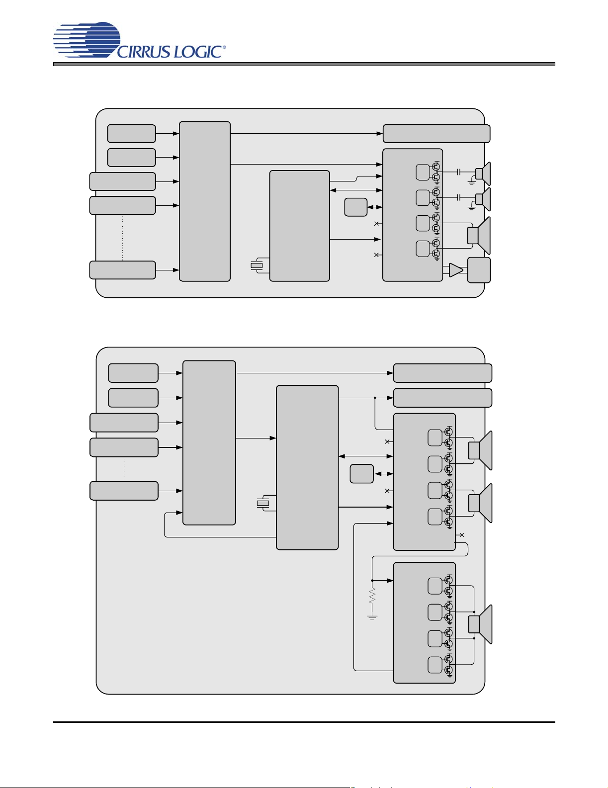
4. TYPICAL SYSTEM CONFIGURATION DIAGRAMS
2 x 7 W Stereo + 1 x 15 W Subwoofer
CS4525
Main Tuner
PIP Tuner
A/V In 1
A/V In 2
A/V In X
Main Tuner
PIP Tuner
A/V In 1
A/V In 2
A/V In X
Digital Out
Control Port
A/V Switch
MPEG
Audio
Delay
Decoder
Clock
Out
27 MHz
Crystal In
Crystal Out
Figure 3. Typical System Configuration 1
2 x 15 W Stereo + 1 x 30 W Subwoofer
Analog
Out
Sound
Processor
Analog
27 MHz
In
Crystal In
Crystal Out
Analog
Out
Control
Port
Clock
Out
Audio
Delay
A/V Switch
CS4525
Analog In
Digital In
Control
Port
Delay
Port
Aux
Out
SYS_CLK
Power
Foldback
Analog In
Digital In
Control
Port
Delay
Port
Aux
Out
SYS_CLK
Power
Foldback
Monitor Out
Gate
Drive
Gate
Drive
Gate
Drive
Gate
Drive
PWM_SIG1
PWM_SIG2
Monitor Out
Var/Fixed Out
CS4525
Gate
Drive
Gate
Drive
Gate
Drive
Gate
Drive
PWM_SIG1
PWM_SIG2
Left
Speaker
Right
Speaker
Subwoofer
HP/
Line
Out
Left
Speaker
Right
Speaker
CS4412A
PWM In
22 kΩ
Status
Out
Gate
Drive
Gate
Drive
Gate
Drive
Gate
Drive
Subwoofer
Figure 4. Typical System Configuration 2
DS726PP2 15
Page 16
2 x 30 W Stereo + 1 x 30 W Subwoofer
CS4525
Main Tuner
PIP Tuner
A/V In 1
A/V In 2
A/V In X
A/V Switch
18.432 MHz
Sound
Processor
Analog
In
Crystal In
Crystal Out
Analog
Out
Analog
Out
Control
Port
Clock
Out
Audio
Delay
Monitor Out
Var/Fixed Out
CS4525
Analog In
Digital In
Control
Port
Delay
Port
Aux
Out
SYS_CLK
Power
Foldback
Gate
Drive
Gate
Drive
Gate
Drive
Gate
Drive
PWM_SIG1
PWM_SIG2
Left
Speaker
CS4412A
PWM In
22 kΩ
Gate
Drive
Gate
Drive
Gate
Drive
Right
Speaker
22 kΩ
Figure 5. Typical System Configuration 3
Status
Out
CS4412A
PWM In
Status
Out
Gate
Drive
Gate
Drive
Gate
Drive
Gate
Drive
Gate
Drive
Subwoofer
16 DS726PP2
Page 17
2 x 15 W Bi-Amp Stereo with Subwoofer Output
CS4525
Main Tuner
PIP Tuner
A/V In 1
A/V In 2
A/V In X
A/V Switch
18.432 MHz
Sound
Processor
Analog
In
Crystal In
Crystal Out
Analog
Out
Analog
Out
Digital
Out
Control
Port
Clock
Out
Audio
Delay
CS4525
Analog In
Digital In
Control
Port
Delay
Port
Aux
Out
SYS_CLK
Power
Foldback
CS4525
Analog In
Digital In
Control
Port
Delay
Port
Aux
Out
SYS_CLK
Power
Foldback
Monitor Out
Var/Fixed Out
Gate
Drive
Gate
Drive
Gate
Drive
Gate
Drive
PWM_SIG1
PWM_SIG2
Gate
Drive
Gate
Drive
Gate
Drive
Gate
Drive
PWM_SIG1
PWM_SIG2
Left
Tweeter
Left
Woofer
Sub
Out
Right
Tweeter
Right
Woofer
Figure 6. Typical System Configuration 4
DS726PP2 17
Page 18
CS4525
5. CHARACTERISTICS AND SPECIFICATIONS
RECOMMENDED OPERATING CONDITIONS
AGND = DGND = PGND = 0 V; all voltages with respect to ground.
Parameters Symbol Min Nom Max Units
DC Power Supply
Digital and Analog Core (Note 1) VD 2.375 2.5 2.625 V
VD 3.135 3.3 3.465 V
VD 4.75 5.0 5.25 V
Amplifier Outputs VP 8.0 - 18.0 V
Temperature
Ambient Temperature Commercial T
Junction Temperature T
A
J
-10 - +70 °C
-10 - +125 °C
Notes: 1. For VD = 2.5 V, VA_REG and VD_REG must be connected to VD. See section 6.7 on page 63 for
details.
ABSOLUTE MAXIMUM RATINGS
AGND = DGND = PGND = 0 V; all voltages with respect to ground.
Parameters Symbol Min Max Units
DC Power Supply
Power Stage Outputs Switching and Under Load
Power Stage No Output Switching
Digital and Analog Core
VP
VP
VD
-0.3
-0.3
-0.3
19.8
23.0
6.0
V
V
V
Inputs
Input Current (Note 2) I
Analog Input Voltage (Note 3) V
Digital Input Voltage (Note 3) V
in
INA
IND
-±10mA
AGND - 0.7 VA_REG + 0.7 V
-0.3 VD + 0.4 V
Temperature
Ambient Operating Temperature - Power Applied
Commercial T
Storage Temperature T
A
stg
-20 +85 °C
-65 +150 °C
WARNING:Operation beyond these limits may result in permanent damage to the device. Normal operation is not
guaranteed at these extremes.
Notes: 2. Any pin except supplies. Transie nt currents of up to ±100 mA on the analog input pins wi ll not cause
SCR latch-up.
3. The maximum over/under voltage is limited by the input current.
18 DS726PP2
Page 19
CS4525
ANALOG INPUT CHARACTERISTICS
Test Conditions (unless otherwise specified): AGND = DGND = PGND = 0 V; All voltages with respect to ground;
T
= 25°C; VD = 3.3 V; Input Signal: 1 kHz sine wave through the recommended passive input filter shown in Fig-
A
ure 28 on page 61; Capacitor values connected to AFILTA, AFILTB, FILT+, VQ, VD_REG, and VA_REG as shown
in Figure 1 on page 13; Sample Frequency = 48 kHz; 10 Hz to 20 kHz Measurement Bandwidth; Power outputs in
power-down state (PDnOut1 = 1, PDnOut2 = 1, PDnOut3/4 = 1).
Parameter Min Typ Max Unit
Dynamic Range (Note 4) A-weighted
unweighted
Total Harmonic Distortion + Noise -1 dB
-20 dB
-60 dB
DC Accuracy
Interchannel Gain Mismatch - 0.05 - dB
Gain Drift - ±100 - ppm/°C
Interchannel Isolation - 90 - dB
Full-scale Input Voltage VD = 2.5V (Note 5)
VD = 3.3V
VD = 5.0V
Input Impedance (Note 6) 40 - - kΩ
90
87
-
-
-
0.786*VD
0.590*VD
0.398*VD
95
92
-86
-72
-32
0.827*VD
0.621*VD
0.419*VD
-
-
-77
-
-
0.868*VD
0.652*VD
0.440*VD
dB
dB
dB
dB
dB
Vpp
Vpp
Vpp
Notes: 4. Referred to the typical full-scale voltage
5. For VD = 2.5 V, VA_REG and VD_REG must be connected to VD. See section 6.7 on page 63 for
details.
6. Measured between AINx and AGND.
ADC DIGITAL FILTER CHARACTERISTICS
Parameter Min Typ Max Unit
Passband (Frequency Response) (Note 7) to -0.1 dB corner 0 - 0.4948 Fs
Passband Ripple -0.09 - 0 dB
Stopband (Note 7) 0.6677 - - Fs
Stopband Attenuation 48.4 - - dB
Total Group Delay - 2.7/Fs - s
High-Pass Filter Characteristics
Frequency Response -3.0 dB
-0.13 dB
Phase Deviation 20 Hz - 10 - Deg
Passband Ripple - - 0.17 dB
Filter Settling Time -10
Notes: 7. Filter response is clock dependent and scales with the ADC sampling frequency (Fs). With a
27.000 MHz or 24.576 MHz XTAL/SYS_CLK, Fs is equal to the applied clock divided by 512. With an
18.432 MHz XTAL/SYS_CLK, Fs is equal to the applied clock divided by 384.
-
-
3.7
24.2
5
/Fs - s
-
-
Hz
Hz
DS726PP2 19
Page 20
CS4525
PWM POWER OUTPUT CHARACTERISTICS
Test Conditions (unless otherwise specified): AGND = DGND = PGND = 0 V; All voltages with respect to ground;
T
= 25°C; VD = 3.3 V; VP = 18 V; RL = 8 Ω for full-bridge, RL = 4 Ω for half-bridge and parallel full-bridge;
A
OutputDly[3:0] = 1111; PhaseShift = 1 for half-bridge, PhaseShift = 0 for full-bridge and parallel full-bridge;
Input Signal: full-scale 997 Hz sine wave through serial audio input port, 48 kHz sample rate; Capacitor values
connected to AFILTA, AFILTB, FILT+, VQ, VD_REG, and VA_REG as shown in Figur e 1 on page 13; PWM Switch
Rate = 384 kHz; 10 Hz to 20 kHz Measurement Bandwidth; Performance measurements taken through AES17 filter.
Parameters Symbol Conditions Min Typ Max Units
Power Output per Channel
Stereo Full-Bridge
Half-Bridge
Parallel Full-Bridge
Total Harmonic Distortion + Noise
Stereo Full-Bridge
Half-Bridge
Parallel Full-Bridge
Dynamic Range
Stereo Full-Bridge
Half-Bridge
Parallel Full-Bridge
MOSFET On Resistance R
P
O
THD+N
DYR
DS(ON)
THD+N < 10%
THD+N < 1%
THD+N < 10%
THD+N < 1%
THD+N < 10%
THD+N < 1%
= 1 W
P
O
PO = 0 dBFS = 11.3 W
= 1 W
P
O
PO = 0 dBFS = 5.0 W
PO = 1 W
= 0 dBFS = 22.6 W
P
O
= -60 dBFS, A-Weighted
P
O
= -60 dBFS, Unweighted
P
O
PO = -60 dBFS, A-Weighted
PO = -60 dBFS, Unweighted
= -60 dBFS, A-Weighted
P
O
PO = -60 dBFS, Unweighted
-
-
-
-
-
-
-
-
-
-
-
-
-
-
-
-
-
-
15
12
7
5.5
30
23.5
0.05
0.10
0.12
0.28
0.1
0.3
102
99
99
96
102
99
-
-
-
-
-
-
-
-
-
-
-
-
-
-
-
-
-
-
Id= 0.5 A, TJ=50°C-280-mΩ
W
W
W
W
W
W
%
%
%
%
%
%
dB
dB
dB
dB
dB
dB
Efficiency h PO = 2 x 15 W, RL = 8 Ω -85-%
Minimum Output Pulse Width PW
Rise Time of OUTx t
Fall Time of OUTx t
PWM Output Over-Current Error Trigger Point
I
Junction Thermal Warning Trigger Point T
Junction Thermal Error Trigger Point T
VP Under-Voltage Error Falling Trigger Point V
VP Under-Voltage Error Rising Trigger Point V
UVFALL
UVRISE
CE
TW
TE
r
f
min
TA = 25°C, OCREF = 16.2 kΩ
T
A
T
A
No Load - 50 - ns
Resistive Load - 20 - ns
Resistive Load - 20 - ns
= 25°C, OCREF = 18 kΩ
= 25°C, OCREF = 22 kΩ
-
-
-
2.5
2.1
1.7
-
-
-
A
A
A
-105-°C
-125-°C
TA = 25°C-4.74.9V
TA = 25°C - 4.95 5.4 V
20 DS726PP2
Page 21
CS4525
SERIAL AUDIO INPUT PORT SWITCHING SPECIFICATIONS
AGND = DGND = PGND = 0 V; TA = 25°C; VD = 3.3 V; Inputs: Logic 0 = DGND; Logic 1 = VD.
Parameters Symbol Min Nominal Max Units
28.5
Supported Input Sample Rates F
LRCK Duty Cycle 45 - 55 %
SCLK Frequency (Note 8),(Note 9) 1/t
SCLK Duty Cycle 45 - 55 %
LRCK Setup Time Before SCLK Rising Edge t
SDIN Setup Time Before SCLK Rising Edge t
SDIN Hold Time After SCLK Rising Edge t
RST
pin Low Pulse Width (Note 10) 1--ms
SI
p
s(LK-SK)
s(SD-SK)
h
39.5
39.5
86.4
FSI*2*N
bits
40 - - ns
25 - - ns
10 - - ns
32
44.1
48
96
-F
35.2
52.8
52.8
105.6
/3 Hz
CLK
kHz
kHz
kHz
kHz
Notes: 8. F
9.
10. After powering up the CS4525, RST
is the frequency of the crystal connected to the XTI/XTO pins or the input SYS_CLK signal.
CLK
N
is the number of bits per sample of the serial digital input.
bits
should be held low until the power supplies and clocks are stab le.
//
LRCK
//
t
P
//
t
t
r
f
t
h
//
//
MSB MSB-1
//
SCLK
SDIN
t
s(LK-SK)
t
s(SD-SK)
Figure 7. Serial Audio Input Port Timing
DS726PP2 21
Page 22
CS4525
g
AUX SERIAL AUDIO I/O PORT SWITCHING SPECIFICATIONS
AGND = DGND = PGND = 0 V; TA= 25°C; VD = 3.3 V; AUX_SDOUT & DLY_SDOUT CL= 15 pF; Inputs:
Logic 0 = DGND; Logic 1 = VD;
Parameters Symbol Min Typ Max Units
Input Source: Analog Inputs (Internal ADC)
Output Sample Rate ClkFreq[1:0] = ‘00’
AUX_LRCK Duty Cycle - 50 - %
AUX_LRCK Period - 1/F
AUX_SCLK Frequency ClkFreq[1:0] = ‘00’
AUX_SCLK Duty Cycle - 50 - %
AUX_SCLK Period - 1/F
Input Source: Serial Audio Input Port
Output Sample Rate F
AUX_LRCK Duty Cycle (Note 13) 45 - 55 %
AUX_LRCK Period (Note 12, 13)T
AUX_SCLK Frequency F
(Note 14) F
AUX_SCLK Duty Cycle 30 - 70 %
AUX_SCLK Period F
(Note 13, 14)F
Input Source: Analog Inputs or Serial Audio Input Port
AUX_LRCK Rising Edge to AUX_SCLK Falling Edge t
AUX_SCLK Rising Edge to Data Output Valid t
DLY_SDIN Setup Time Before AUX_SCLK Rising Edge t
DL Y_SDIN Hold Time After AUX_SCLK Rising Edge t
(Note 11).
ClkFreq[1:0] = ‘01’
ClkFreq[1:0] = ‘10’
ClkFreq[1:0] = ‘01’
ClkFreq[1:0] = ‘10’
= 32kHz, 44.1 kHz, 48 kHz
S-In
F
S-In
= 32kHz, 44.1 kHz, 48 kHz
S-In
S-In
= 32kHz, 44.1 kHz, 48 kHz
S-In
S-In
=96kHz
=96kHz
=96kHz
F
F
SCLKO
F
LTSF
SRDV
DIS
DIH
SO
SO
T
2*T
SI
SCLKI
SCLKI
- T
-
-
-
-
-
-
-
-
CLK
-
-
- T
- T
CLK
CLK
F
CLK
F
CLK
F
CLK
48*F
64*F
64*F
F
F
T
2*T
/384
/512
/512
SO
SCLKO
F
SI
FSI/2
T
SI
SCLKI
SCLKI
SCLKI
SCLKI
SO
SO
SO
TSI + T
/2
T
SCLKI
2*T
SCLKI
- - 20 ns
--T
CLK
25 - - ns
10 - - ns
-
-
-
Hz
Hz
Hz
-s
-
-
-
Hz
Hz
Hz
-s
-
-
CLK
-
-
+ T
+ T
CLK
CLK
Hz
Hz
s
Hz
Hz
s
s
+ 20 ns
Notes: 11. F
12. F
is the frequency of the crystal connected to the XTI/XTO pins or the input SYS_CLK signal.
CLK
T
=1/F
CLK
is the frequency of the input LRCK signal. TSI=1/F
SI
CLK
.
SI
13. May vary during normal operation.
14. F
is the frequency of the input SCLK signal. T
SCLKI
AUX_LRCK
AUX_SCLK
AUX_SDOUT
DLY_SDOUT
DLY_SDIN
LSB
LSB
t
DISU
t
LTSF
MSB
MSB
SCLKI
=1/F
t
SRDV
t
DIH
SCLKI
MSB - 1
MSB - 1
.
Figure 8. AUX Serial Port Interface Master Mode Timin
22 DS726PP2
Page 23
CS4525
XTI SWITCHING SPECIFICATIONS
Parameter Symbol Min Typ Max Unit
External Crystal Operating Frequency ClkFreq[1:0] = ‘00’
(Note 15) ClkFreq[1:0] = ‘01’
ClkFreq[1:0] = ‘10’
XTI Duty Cycle 45 50 55 %
F
CLK
18.240
24.330
26.730
18.432
24.576
27.000
18.617
24.822
27.270
MHz
MHz
MHz
Notes: 15. See “Clock Frequency (ClkFreq[1:0])” on page 69.
SYS_CLK SWITCHING SPECIFICATIONS
AGND = DGND = PGND = 0 V; TA = 25°C; VD = 3.3 V; Input: Logic 0 = DGND; Logic 1 = VD, SYS_CLK Output:
=20pF.
C
L
Parameter Symbol Min Typ Max Unit
External Clock Operating Frequency ClkFreq[1:0] = ‘00’
(Note 15) ClkFreq[1:0] = ‘01’
ClkFreq[1:0] = ‘10’
Rising Edge RST
SYS_CLK Period t
SYS_CLK Duty Cycle 45 50 55 %
SYS_CLK high time t
SYS_CLK low time t
to start of SYS_CLK t
F
sclko
CLK
sclki
clkih
clkil
18.240
24.330
26.730
- 1024*t
37.04 - 54.25 ns
16.67 - 29.84 ns
16.67 - 29.84 ns
18.432
24.576
27.000
sclki
18.617
24.822
27.270
-
MHz
MHz
MHz
t
SYS_CLK
(output)
___
RST
sclko
Figure 9. SYS_CLK Timing from Reset
PWM_SIGX SWITCHING SPECIFICATIONS
AGND = DGND = PGND = 0 V; TA = 25°C; VD = 3.3 V; Load = 10 pF.
Parameter Symbol Min Typ Max Unit
Rise Time of PWM_SIGx t
Fall Time of PWM_SIGx t
t
r
PWM_SIGx
Figure 10. PWM_SIGX Timing
r
f
t
f
-2.1-ns
-1.4-ns
DS726PP2 23
Page 24
CS4525
I²C CONTROL PORT SWITCHING SPECIFICATIONS
AGND = DGND = PGND = 0 V; TA = 25°C; VD = 3.3 V; Inputs: Logic 0 = DGND; Logic 1 = VD; SDA CL=30pF.
Parameter Symbol Min Max Unit
SCL Clock Frequency f
Rising Edge to Start t
RST
Bus Free Time Between Transmissions t
Start Condition Hold Time (prior to first clock pulse) t
Clock Low time t
Clock High Time t
Setup Time for Repeated Start Condition t
SDA Hold Time from SCL Falling (Note 16) t
SDA Setup time to SCL Rising t
Rise Time of SCL and SDA t
Fall Time SCL and SDA t
Setup Time for Stop Condition t
Acknowledge Delay from SCL Falling t
scl
irs
buf
hdst
low
high
sust
hdd
sud
rc
fc
susp
ack
- 100 kHz
500 - ns
4.7 - µs
4.0 - µs
4.7 - µs
4.0 - µs
4.7 - µs
10 - ns
250 - ns
-1µs
- 300 ns
4.7 - µs
300 1000 ns
Notes: 16. Data must be held for sufficient time to bridge the transition time, t
RST
t
SDA
SCL
irs
Stop Start
t
buf
t
hdst
t
low
t
hdd
t
high
t
sud
Repeated
Start
t
sust
t
hdst
Figure 11. Control Port Timing - I²C
, of SCL.
fc
t
r
Stop
t
f
t
susp
24 DS726PP2
Page 25
CS4525
DC ELECTRICAL CHARACTERISTICS
AGND = DGND = PGND = 0 V; All voltages with respect to ground; PWM switch rate = 384 kHz; Unless otherwise
specified.
Parameters Min Typ Max Units
Normal Operation
Power Supply Current VD = 3.3 V - 54 - mA
Power Dissipation VD = 3.3 V - 180 - mW
Power-Down Mode (Note 18)
Power Supply Current VD = 3.3 V - 2.8 - mA
VD_REG Characteristics
Nominal Voltage 2.25 2.5 2.75 V
DC current source - - 3 mA
VA_REG Characteristics
Nominal Voltage 2.25 2.5 2.75 V
DC current source - - 1 mA
VQ Characteristics
Nominal Voltage - 0.5*VA_REG - V
Output Impedance - 23 - kΩ
DC current source/sink (Note 19) --10μA
Filt+ Nominal Voltage - VA_REG - V
Power Supply Rejection Ratio (Note 20) 1 kHz
(Note 17)
60 Hz
-
-
60
40
-
-
dB
dB
Notes: 17. Normal operation is defined as RST
18. Power-Down Mode is defined as RST
= HI.
= LOW with all input lines held static.
19. The DC current drain represents the allowed current from the VQ pin due to typ ica l leakag e thr ough
the electrolytic de-coupling capacitors.
20. Valid with the recommended capacitor values on FILT+ and VQ. Increasing the capacitance will
increase the PSRR.
DIGITAL INTERFACE SPECIFICATIONS
AGND = DGND = PGND = 0 V; All voltages with respect to ground; Unless otherwise specified.
Parameters Symbol Min Max Units
Digital Interface Signal Characteristics
High-Level Input Voltage V
Low-Level Input Voltage V
High-Level Output Voltage Io=2 mA
Low-Level Output Voltage Io=2 mA
Input Leakage Current I
Input Capacitance - 8 pF
PWM_SIGx Characteristics
High-Level PWM_SIGx Output Voltage Io=2 mA
Low-Level PWM_SIGx Output Voltage Io=2 mA
(Note 21)
V
V
V
V
IH
IL
OH
OL
in
OHPS
OLPS
0.75*VD_REG - V
- 0.20*VD_REG V
0.90*VD - V
-0.2V
-±10uA
0.90*VD_REG - V
-0.2V
Notes: 21. Digital interface signals include all pins sourced from the VD supply as shown in “Digital I/O Pin
Characteristics” on page 12.
DS726PP2 25
Page 26
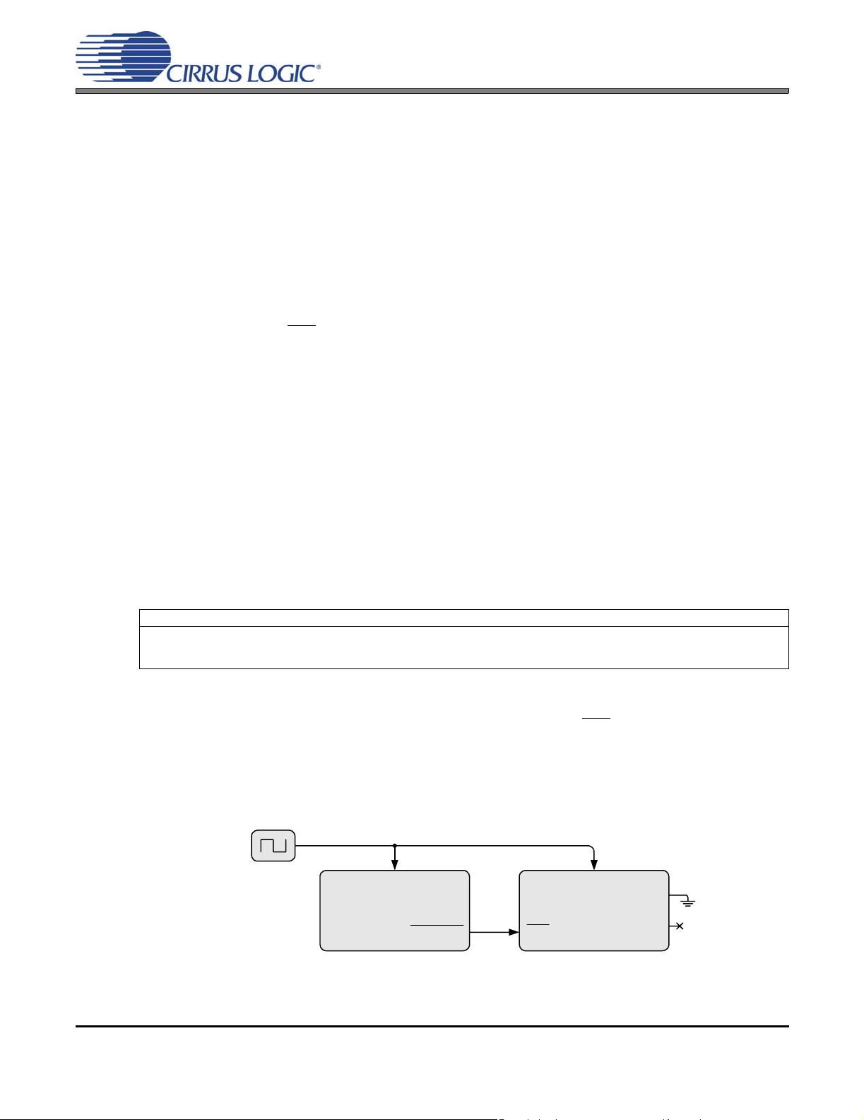
6. APPLICATIONS
6.1 Software Mode
Maximum device flexibility and features are available when the CS4525 is used in software mode. The available features are described in the following sections. All device configu ration is achieved via the I²C control
port as described in the I²C Control Port Description and Timing section on page 64.
6.1.1 System Clocking
In software mode, the CS4525 can be clocked by a stable external clock source input on the SYS_CLK
pin or by a clock internally generated through the use of its internal oscillator driver circuit in conjunction
with an external crystal oscillator. The device automatically selects which of these clocks to use within
10 ms of the re lea se of RST
The internal clock is used to synchronize the input serial audio signals with the internal clock domain and
to clock the internal digital processing, sample-rate con verter, and PWM modulators. It is also used to determine the sample rate of the serial audio input signals in order to automatically co nfigure the various
internal filter coefficients.
To ensure proper operation, the CS4525 must be informed of the nominal frequency of the supplied
SYS_CLK signal or the attached crystal via the ClkFreq[1:0] bits in the Clock Config register. These bits
must be set to the appropriate value before the PDnAll bit is cleared to initiate a power-up sequence. See
the SYS_CLK Switching Specifications and XTI Switching Specifications tables on page 23 for complete
input frequency range specifications.
CS4525
.
WARNING: The system clock source must never be removed or stopped while any of the power output
stages are powered-up (the PDnAll bit and any of the PDnOut1, PDnOut2, or PDnOut3/4 bits are cleared)
and connected to a load. Doing so may result in permanent dam age to the CS4525 and connected tra nsducers.
Referenced Control Register Location
ClkFreq[1:0]......................... “Clock Frequency (ClkFreq[1:0])” on page 69
PDnAll.................................“Power Down (PDnAll)” on page 89
PDnOutX............................. “Power Down PWM Power Output X (PDnOutX)” on page 88
6.1.1.1 SYS_CLK Input Clock Mode
If an input clock is detected on the SYS_CLK pin following the release of RST, the device will automatically
use the SYS_CLK input as its clock source. The applied SYS_CLK clock signal must oscillate within the
frequency ranges specified in the SYS_CLK switching specifications table on page 23. In this mode, XTI
should be connected to ground and XTO should be left unconnected.
Figure 12 below demonstrates a typical clocking configuration using the SYS_CLK input.
Clock
Clock_In
DSP
Reset_Out
RST
SYS_CLK
CS4525
XTI
XTO
Figure 12. Typical SYS_CLK Input Clocking Configuration
26 DS726PP2
Page 27
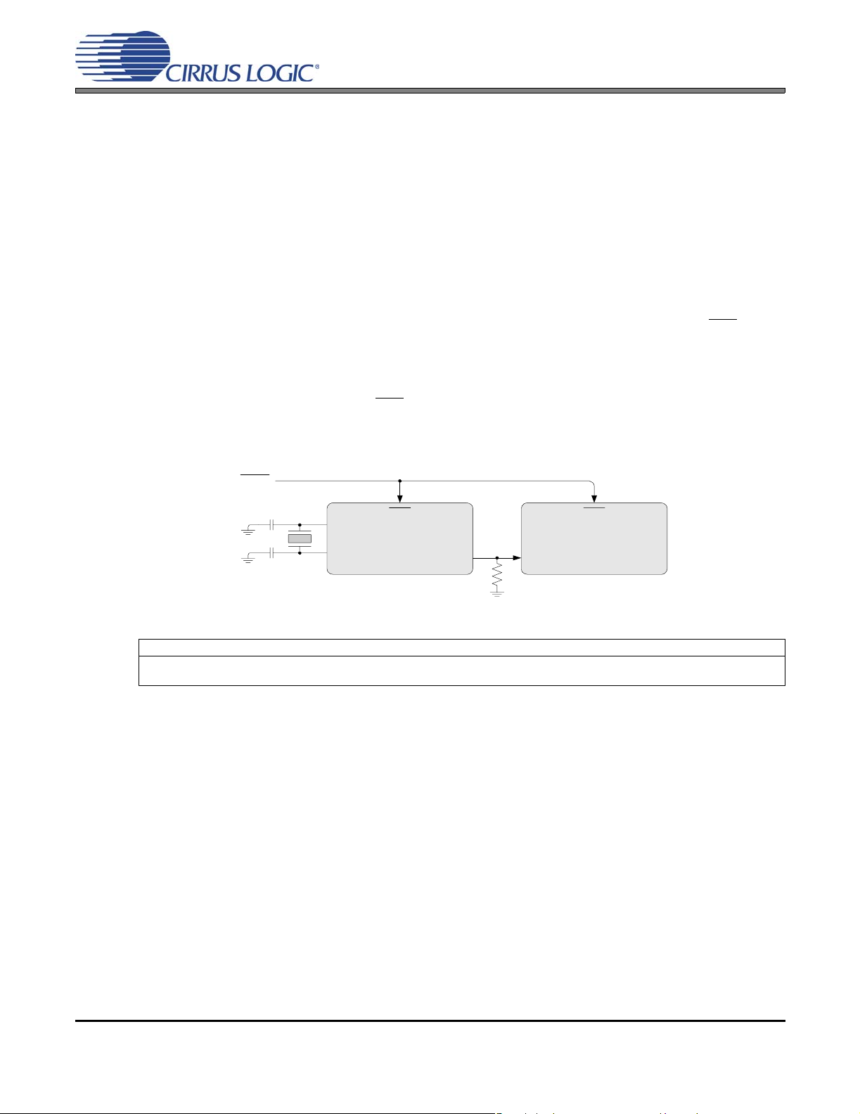
CS4525
6.1.1.2 Crystal Oscillator Mode
To use an external crystal in conjunction with the internal crystal driver, a 20 pF fundamental mode parallel resonant crystal must be connected between the XTI and XTO pins. This crystal must oscillate within
the frequency ranges specified in the XTI switching specifications table on page 23. Nothing other than
the crystal and its load capacitors should be connected to XTI and XTO. The SYS_CLK pin should be
connected to ground through a 22 kΩ pull-down resistor to prevent the CS4525 from r ecogn izing syste m
noise on the SYS_CLK pin as a valid clocking signal.
In this mode, the CS4525 will automatically drive the generated internal clock out of the SYS_CLK pin.
This can be disabled with the EnSysClk bit which will cause the SYS_CLK pin to become high-impedance.
Also, the DivSysClk bit allows the frequency of the generated internal clock to be divided by 2 prior to being driven out of the SYS_CLK.
It should be noted that the internal oscillator driver is disabled when the CS4525 is in reset (RST
is low).
Any external devices connected to the SYS_CLK output will not receive a clock signal until the CS4525
is taken out of reset.
If an external crystal is connected to the XTI/XTO pins while an input clock signal is present on the
SYS_CLK pin following the release of RST
, then the CS4525 will automatically use the SYS_CLK pin for
its internal clock. Refer to Section 6.1.1.1 for a details about this mode of operation.
Figure 13 below demonstrates a typical clocking configuration using the crystal oscillator.
Reset
XTI
XTO
RST RST
CS4525
SYS_CLK Clock_In
DSP
Figure 13. Typical Crystal Oscillator Clocking Configuration
Referenced Control Register Location
EnSysClk.............................“SYS_CLK Output Enable (EnSysClk)” on page 69
DivSysClk............................ “SYS_CLK Output Divider (DivSysClk)” on page 69
DS726PP2 27
Page 28

6.1.2 Power-Up and Power-Down
The CS4525 will remain in a completely powered-down state with the control port inaccessible until the
RST
pin is brought high. Once RST is high, the control port will be accessible, but all other internal blocks
will remain powered-down until they are powered-up via the control port or until hardware mode is entered.
When an external crystal is present on the XTI/XTO pins, software mode will be automatically entered
10 ms a fter the re lease of RST
. If SYS_CLK is used as an input, software mode is entered by writing to
the control port within 10 ms after the release of RST
device will begin to operate in hardware mode.
6.1.2.1 Recommended Power-Up Sequence
1. Hold RST low until the power supplies and the input SYS_CLK (if used) are stable.
2. Bring RST
The device will remain in a low-power state and the control port will be accessible. The device will
automatically enter software mode after 10 ms if an external crystal is present on the XTI/XTO pins,
at which time the output SYS_CLK signal will become active.
3. If SYS_CLK is used as an input, initiate a control port write to set the PDnAll bit in register 5Fh within
10 ms following the release of RST
This operation causes the device to enter software mode and places it in power-down mode.
4. If the LVD pin is tied low and VD, VD_REG, and VA_ REG are connected to 2.5 V, clear the SelectVD
bit in the Power Ctrl register to indicate the 2.5 V VD supply level. See section 6.7 on page 63 for details.
5. If VP is connected to a supply voltage less than or equal to 14 V nominal, clear the SelectVP bit in the
Foldback Cfg register to indicate the VP supply level.
6. The desired register settings can be loaded while keeping the PDnAll bit set. Typical initialization set-
tings include Input Configuration, Output Configuration, Master Volume, and Clock Frequency.
7. Clear the PDnAll bit to initiate the power-up sequence.
high.
CS4525
. If the control port is not written within this time, the
.
6.1.2.2 Recommended Power-Down Sequence
1. Set the MuteChA, MuteChB, and MuteSub bits in the Mute Control register to mute the audio outp ut.
2. Set the PDnAll bit to power-down the device.
3. Bring RST
4. Remove power.
Referenced Control Register Location
PDnAll.................................“Power Down (PDnAll)” on page 89
SelectVD.............................“Select VD Level (SelectVD)” on page 88
SelectVP ............................. “Select VP Level (SelectVP)” on page 74
MuteChX.............................“Independent Channel A & B Mute (MuteChX)” on page 84
MuteSub.............................. “Sub Channel Mute (MuteSub)” on page 85
Input Configuration..............“Input Configuration (Address 02h)” on page 71
Output Configuration........... “Output Configuration (Address 04h)” on page 73
Master Volume.................... “Master Volume Control (Address 57h)” on page 82
Clock Frequency.................“Clock Frequency (ClkFreq[1:0])” on page 69
28 DS726PP2
low to bring the device’s power consumption to an absolute minimum.
Page 29
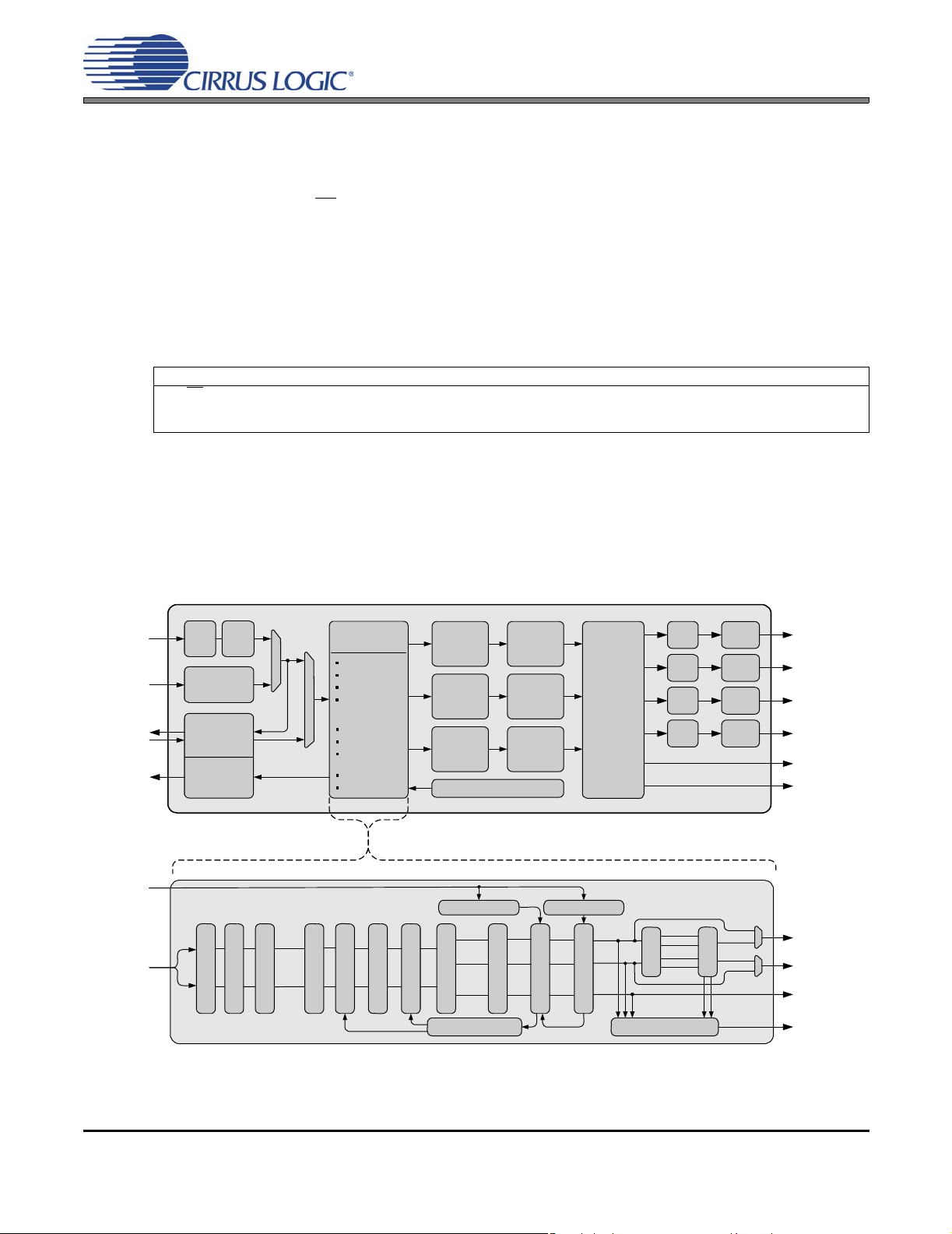
6.1.3 Input Source Selection
The CS4525 can accept analog or digital audio input signals. Digital audio input signals are supplied
through the serial audio input port as outlined in “Ser ial Audio In terfaces” o n page62. Analog audio input
signals are supplied through the internal ADC as outlin ed in “Analog Inputs” on p age 61. The input source
is selected by the ADC/SP
bit in the Input Config register.
In software mode, the serial audio input port supports I²S, Left-Justified and Right-Justified data formats.
The serial audio input port digital interface format is configured by the DIF[2:0] bits in the Input Conf ig register.
The CS4525 internal ADC includes a dedicated high-pass filter to remove any DC content from the ADC
output signal prior to the internal ADC/serial audio input port in put multiplexor. This high-pass filter can be
bypassed by clearing the EnAnHPF bit.
Referenced Control Register Location
ADC/SP............................... “Input Source Selection (ADC/SP)” on page 71
DIF[2:0] ............................... “Input Serial Port Digital Interface Format (DIF [2:0])” on page 71
EnAnHPF............................“ADC High-Pass Filter Enable (EnAnHPF)” on page 71
6.1.4 Digital Sound Processing
The CS4525 implements flexible digital sound processing operation s including ba ss manageme nt crossover, 2-way speaker crossovers, high- and low-pass shelving filters, programmabl e parametric EQ filters,
adaptive loudness compensation, channel mixers, and volume controls.
CS4525
Stereo
Analog In
Serial Audio
Clocks & Data
Serial Audio
Data I/O
Serial Audio
Clocks & Data
Temperature
Sense
Serial Audio
Data In
The digital signal flow is shown in Figure 14 below. The signal processing blocks are described in detail
in the following sections.
ADC
Left
Right
HighPass
Serial Audio
Input Port
Serial Audio
Delay
Interface
Auxiliary
Serial Port
Pre-Scaler
Audio
Processing
Parametric EQ
High-Pass
Bass/Treble
Adaptive
Loudness
Compensation
2-Ch Mixer
2.1 Bass Mgr
Linkwitz-Riley
Crossover
De-Emphasis
Volume
Ch. A
Mixer
Ch. B
High-Pass Filter
De-Emphasis
Param. EQ
Bass Tone Ctrl
Sample
Ch. 1
Rate
Converter
Sample
Ch. 2
Rate
Converter
Sample
Sub
Rate
Converter
Temperature Sense
Thermal Foldback Thermal Limiter
Ch. A
Ch. B
Sub
Bass Manager
Treble Tone Ctrl
Loudness
Modulator
Modulator
Modulator
Ch. Vol Control
PWM
PWM
PWM
PWM
Output
Config
Limiter
Master Vol Control
Aux Serial Data Select
Gate
Drive
Gate
Drive
Gate
Drive
Gate
Drive
Ch. A HPF
Ch. A LPF
Ch. B HPF
X-Over
Ch. B LPF
Ch. B HPF Ch. B LPF
Ch. A HPF
Ch. A LPF
Sensitivity
Power
Stage
Power
Stage
Power
Stage
Power
Stage
Ch. A
Ch. B
Amplifier
Out 1
Amplifier
Out 2
Amplifier
Out 3
Amplifier
Out 4
PWM Modulator
Output 1
PWM Modulator
Output 2
Ch. 1
Ch. 2
Sub
Data to
Aux Port
Figure 14. Digital Signal Flow
DS726PP2 29
Page 30
CS4525
6.1.4.1 Pre-Scaler
Applying any gain to a full-scale signal in the digital domain will cause the signal to clip. To prevent this,
a pre-scaler block is included prior to the internal digital signal processing blocks. This allows the input
signal to be attenuated before processing to ensure that any signal boosting, such as gain in a shelving
filter, will not cause a channel to clip.
The pre-scaler block allows up to -14.0 dB of attenuation in 2.0 dB increments and is controlled with the
PreScale[2:0] bits.
Referenced Control Register Location
PreScale[2:0].......................“Pre-Scale Attenuation (PreScale[2:0])” on page 75
6.1.4.2 Digital Signal Processing High-Pass Filter
The CS4525 includes a high-pass filter at the beginning of the digital signal processing chain to remove
any DC content from the input signal prior to the remaining internal digital signal processing blocks. The
high-pass filter operates by continuously subtracting a measure of the DC offset from the inpu t signal and
may be used regardless of the input data source.
The digital signal processing high-pass filter can be disabled by clearing the EnDigHPF bit.
Referenced Control Register Location
EnDigHPF...........................“Digital Signal Processing High-Pass Filter (EnDigHPF)” on page 77
6.1.4.3 Channel Mixer
The CS4525 implements independent channel mi xers to provide for b oth mono mixes and channel swap s
for the left and right channels. The channel mi xers are controlled by the LChMix[1:0] and RChMix[1:0] bits
in the Mixer Config register.
To allow stereo operation when a mono mix is configured, when the HP_DETECT/MUTE pin is con figured
for headphone detection (the HP/Mute
active state of the headphone detection input signal. In this configuration, when the left channel mixer is
configured for a mono mix (LChMix[1:0] = 01 or 10) and the headphone detection input signal becomes
active, the left channel mixer will be automatically reconfigured to output the left channel, thereby disabling the mono mix. When the headphone detection input signal becomes inactive, the mixer will be automatically reconfigured to operate as dictated by the LChMix[1:0] bits.
It should be noted that the right channel mixer output is un affected by the head phone detectio n input signal and will always operate as dictated by the RChMix[1:0] bits.
Referenced Control Register Location
LChMix[1:0]......................... “Left Channel Mixer (LChMix[1:0])” on page 76
RChMix[1:0] ........................ “Right Channel Mixer (RChMix[1:0])” on page 76
HP/Mute
..............................“HP_Detect/Mute Pin Mode (HP/Mute)” on page 70
bit is set), the operation of the left channel mixer is affecte d by the
30 DS726PP2
Page 31

CS4525
6.1.4.4 De-Emphasis
The CS4525 includes an on-chip digital de-emphasis filter optimized for a sample rate of 44.1 kHz to accommodate audio recordings that utilize 50/15 μs pre-emphasis equalization as a means of noise reduction. The filter response is shown in Figure 15. The de-emphasis filter is enabled and disabled by the
DeEmph bit in the Tone Config register.
Gain (dB)
0 dB
-10 dB
Nominal Sample Rate
96 kHz 0.03609 Fs 0.12030 Fs
T1=50 µs
F1 F2
0.07218 Fs
T2 = 15 µs
Frequency
Normalized to Fs
0.24059 Fs32 kHz, 44.1 kHz, 48 kHz
(Hz)
Figure 15. De-Emphasis Filter
Referenced Control Register Location
DeEmph..............................“De-Emphasis Control (DeEmph)” on page 76
6.1.4.5 Tone Control
The CS4525 implements configurable bass and treble shelving filters to easily accommodate system tone
control requirements. Each shelving filter has 4 selectable corner frequencies, and provides a cut/boost
range from -10.5 dB to +12.0 dB in 1.5 dB increments. The tone control is enabled by the EnToneCtrl bit
in the Tone Config register.
Each tone control is implemented with one of two preset internal filter sets. One set is optimized for a
32 kHz sample rate, and the other is optimized for 44.1 kHz, 48 kHz, and 96 kHz sample rates. The
CS4525 automatically detects the input sample rate and chooses the appropriate filter set to apply. The
available corner frequencies are shown in tables 2 and 3 below and are configured with the BassFc[1 :0]
and TrebFc[1:0] bits in the Tone Config register.
Note that the corner frequency of each filter set scales linearly with the input sample rate.
When the internal ADC is used as the serial audio data sour ce, the input sample rate is nominally 48 kHz
and the corresponding shelving frequency corners are available.
Input Sample Rate Bass Fc 0 Bass Fc 1 Bass Fc 2 Bass Fc 3
32 kHz 50 Hz 100 Hz 200 Hz 250 Hz
44.1kHz 48Hz 96Hz 192Hz 240Hz
48 kHz, 96 kHz 52 Hz 104 Hz 208 Hz 260 Hz
Table 2. Bass Shelving Filter Corner Frequencies
DS726PP2 31
Page 32

CS4525
Input Sample Rate Treble Fc 0 Treble Fc 1 Treble Fc 2 Treble Fc 3
32 kHz 5.0 kHz 7.0 kHz 10.0 kHz 15.0 kHz
44.1 kHz 4.8 kHz 6.7 kHz 9.6 kHz 14.4 kHz
48 kHz, 96 kHz 5.2 kHz 7.3 kHz 10.4 kHz 15.6 kHz
Table 3. Treble Shelving Filter Corner Frequencies
The cut/boost level of the bass and treble shelving filters are set by the Bass[3:0] and Treble[3:0] bits in
the Tone Control register.
Referenced Control Register Location
EnToneCtrl .......................... “Tone Control Enable (EnToneCtrl)” on page 77
TrebFc[1:0].......................... “Treble Corner Frequency (TrebFc[1:0])” on page 77
BassFc[1:0].........................“Bass Corner Frequency (BassFc[1:0])” on page 77
Treble[3:0]........................... “Treble Gain Level (Treb[3:0])” on page 78
Bass[3:0].............................“Bass Gain Level (Bass[3:0])” on page 78
32 DS726PP2
Page 33

6.1.4.6 Parametric EQ
The CS4525 implements 5 fully programmable parametric EQ filters.
The filters are implemented in the bi-quad form shown below.
CS4525
x[n] y[n]
-1
Z
-1
Z
b
0
-1
Z
b
1
b
2
a
1
-1
Z
a
2
Figure 16. Bi-Quad Filter Architecture
This architecture is represented by the equatio n shown below where y[n] represents the output sample
value and x[n] represents the input sample value.
y[n] = b
x[n] + b1x[n-1] + b2x[n-2] + a1y[n-1] + a2y[n-2]
0
Equation 1. Bi-Quad Filter Equation
The coefficients are represented in binary form by 24-bit signed values stored in 3.21 two’s complement
format. The 3 MSB’s represent the sign bit and the w hol e-number portion of the decimal coefficient, and
the 21 LSB’s represent the fractional portion of the decimal coefficient. The coefficient values must be in
the range of -4.00000 decimal (80 00 00 hex) to 3.99996 decimal (7F FF FF hex).
The binary coefficient values are stored in registers 0Ah - 54h. Each 24-bit coefficient is split into 3 bytes,
each of which is mapped to an individually accessible register location. See the “Register Quick Refer-
ence” section beginning on page 66 for the specific register locations for each coefficient.
By default, all b
coefficients are set to 1 decimal, and all other coefficients are set to 0 decimal. This im-
0
plements a pass-through function.
The parametric equalizers be independently enabled and disabled for channels A and B with the En-
ChAPEq and EnChBPEq bits located in the EQ Config register.
Referenced Control Register Location
EnChAPEq.......................... “Enable Channel A Parametric EQ (EnChAPEq)” on page 79
EnChBPEq.......................... “Enable Channel B Parametric EQ (EnChBPEq)” on page 79
DS726PP2 33
Page 34

CS4525
6.1.4.7 Adaptive Loudness Compensation
The CS4525 includes adaptive loudness compensation to enhance the audibility of program material at
low volume levels. The adaptive loudness compensation feature operates by varying the bass and treble
boost of the tone control shelving filters as the volume level changes.
The level of boost added to the shelv ing f ilt ers is de termined by the average of the effective volume settings of channels A and B after the master volume control. As this average volume setting decreases from
0 dB, the boost of the bass and treble shelving filters is gradually increased until it reaches the maximum
boost level of 12.0 dB. As the volume is increased, the boost applied due to the adaptive loudness compensation feature will be gradually removed until it reaches the level specified by the Treble[3:0] and
Bass[3:0] bits in the Tone Control register.
The adaptive loudness compensation feature is enabled by setting the Loudness bit in the Tone Config
register. When the loudness feature is enabled, it immediately evaluates the effective average volume a nd
applies bass and treble boost accordingly. When disabled, any treble or bass boost applied due to the
loudness feature will be removed.
Because the adaptive loudness compensation filter op erates by adjusting th e boost level of the tone control shelving filters, it is necessary that they be enabled with the EnToneCtrl bit in the Tone Config register
in order for the loudness feature to be operational. If the ton e control filters are disabled, the adaptive loudness compensation feature will not be functional.
Referenced Control Register Location
Loudness............................. “Adaptive Loudness Compensation Control (Loudness)” on page 76
EnToneCtrl .......................... “Tone Control Enable (EnToneCtrl)” on page 77
TrebFc[1:0].......................... “Treble Corner Frequency (TrebFc[1:0])” on page 77
BassFc[1:0].........................“Bass Corner Frequency (BassFc[1:0])” on page 77
Treble[3:0]........................... “Treble Gain Level (Treb[3:0])” on page 78
Bass[3:0].............................“Bass Gain Level (Bass[3:0])” on page 78
34 DS726PP2
Page 35

CS4525
6.1.4.8 B ass Management
The CS4525 implements a dedicated stereo 24 dB/octave Linkwitz-Riley crossover with adjustable crossover frequency to achieve bass management for 2.1 configurations. The filter’s stereo high-pass outputs
are used to drive the full-range speakers, and its stereo low-pass outputs are each attenuated by 6 dB
and summed to drive the sub channel.
The bass management crossover is implemented with one of two preset internal filter sets. One set is optimized for a 32 kHz sample rate, and the other is optimized for 44.1 kHz, 48 kHz, and 96 kHz sample
rates. The CS4525 automatically detects the input sample rate and chooses the appropriate filter set to
apply. The available bass management cross-over frequencies are shown in Table 4 below and are configured with the BassMgr[2:0] bits in the EQ Config register.
Note that the corner frequency of each filter set scales linearly with the input sample rate.
When the internal ADC is used as the serial audio data sour ce, the input sample rate is nominally 48 kHz
and the corresponding shelving frequency corners are available.
Input Sample Rate
32 kHz 44.1 kHz 48 kHz, 96 kHz
Bass Manager Freq 1 80 Hz 77 Hz 83 Hz
Bass Manager Freq 2 120 Hz 115 Hz 125 Hz
Bass Manager Freq 3 160 Hz 153 Hz 167 Hz
Bass Manager Freq 4 200 Hz 192 Hz 209 Hz
Bass Manager Freq 5 240 Hz 230 Hz 250 Hz
Bass Manager Freq 6 280 Hz 268 Hz 292 Hz
Bass Manager Freq 7 320 Hz 307 Hz 334 Hz
Table 4. Bass Management Cross-Over Frequencies
The BassMgr[2:0] bits also allow the bass manager to be disabled. Whe n disabled, the bass management
crossover is bypassed and no signal is presented on the sub channel.
To allow full-range headphone operati on, when t he HP_DETECT/MUTE pin is configu red for headph one
detection (the HP/Mute
bit is set), the operation of the bass manager is affected by the active state of the
headphone detection input signal. In this configuration, when the bass manager is en abled, (BassMgr[2:0]
bits not equal to ‘000’) and the headphone detection input signal becomes active, the bass manager will
be automatically disabled. When the headphone detection input signal becomes inactive, the bass manager will be automatically reconfigured to operate as dictated by the BassMgr[2:0] bits.
Referenced Control Register Location
BassMgr[2:0]....................... “Bass Cross-Over Frequency (BassMgr[2:0])” on page 79
HP/Mute
..............................“HP_Detect/Mute Pin Mode (HP/Mute)” on page 70
DS726PP2 35
Page 36

CS4525
6.1.4.9 Volume and Muting Control
The CS4525’s volume control architecture provides the ability to control the level of each output channel
on both an individual and master basis.
Individual control allows the volume and mute state of a single channel to be changed ind ependently from
the other channels within the device. The CS4525 provides three individual volume and muting controls,
each permanently assigned to one channel within the device. The three individual volume controls,
ChAVol, ChBVol, and SubVol, can gain or attenuate channel A, channel B, or the sub channel (respectively) from +24 dB to - 103 dB in 0.5 dB steps. The three individual mute contro ls, MuteChA, MuteChB,
and MuteSub bits, can mute channel A, channel B, or the sub channel (respectively).
Master control allows the volume of all channels to be changed simultaneously by offsetting each channel’s individual volume setting by an additional +24 dB to -103 dB in 0.5 dB steps. By default, master volume is set to +3dB; if the CS4525 is being used to control the application’s master volume, then it is
recommended to change this value to a comfortable listening level befo re enabling the PWM powered outputs. Master volume control is accomplished via the Master Vol register.
The PWM outputs can be configured to output silence as a modulated signal or an non-modulated 50%
duty cycle signal during a mute condition. This selection is achieved via the Mute50/50 bit in the
Volume Cfg register.
The AutoMute bit in the same register dictates whether the device will automatically mute after the reception of 8192 consecutive samples of static 0 or -1. When the AutoMute function is enabled, a single sample
of non-static data will cause the automatic mute to be released.
The CS4525 implements soft-ramp and zero-crossing detection capabilities to provide noise-free level
transitions. When the zero-crossing function is enabled, all volume and muting changes are made on an
output signal zero-crossing. The zero-crossing detection function is impleme nted ind epend ently for each
channel. When the soft-ramp function is enabled, the volume is ramped from its initial to its final level at
a rate of ½ dB every 4 samples for 32, 44.1, an d 48 kHz sample rates, and ½ dB every 8 samp les for a
96 kHz sampling rate.
All volume and muting changes are implemented as dictated by the soft-ramp and zero-cross settings
configured by the SZCMode[1:0] bits in the Volume Cfg register.
Referenced Control Register Location
ChXVol................................ “Channel A and B Volume Control (Address 58h & 59h)” on page 83
SubVol................................. “Sub Channel Volume Control (Address 5Ah)” on page 83
MuteChX.............................“Independent Channel A & B Mute (MuteChX)” on page 84
MuteSub.............................. “Sub Channel Mute (MuteSub)” on page 85
Master Vol........................... “Master Volume Control (Address 57h)” on page 82
Mute50/50...........................“Enable 50% Duty Cycle for Mute Condition (Mute50/50)” on page 80
AutoMute............................. “Auto-Mute (AutoMute)” on page 80
SZCMode............................ “Soft Ramp and Zero Cross Control (SZCMode[1:0])” on page 80
36 DS726PP2
Page 37

CS4525
6.1.4.10 Peak Signal Limiter
When enabled, the limiter monitors the digital output following the volume control block, detects when
peak levels exceed a selectable maximum threshold level and lowers the volume at a programmable attack rate until the signal peaks fall below the maximum threshold. When the signal level falls below a selectable minimum threshold, the volume returns to its original level (as determined by the individual and
master volume control registers) at a programmable release rate. Attack and release rates are affected
by the soft ramp/zero cross settings and sample rate, Fs.
Recommended settings: Best limiting performance may be realized with the fastest attack and slowest
release setting with soft ramp enabled in the control registers. Use the “minimum” bits to set a threshold
slightly below the maximum threshold to cushion the sound as the limiter attacks and releases.
Input
Max[2:0]
Limiter
Attack/Release Sound
Volume
Cushion
Attack/Release Sound
Cushion
Output
(after Limiter)
Min[2:0]
RRate[5:0]ARate[5:0]
Figure 17. Peak Signal Detection & Limiting
By default, the limiter affects all channels when the maximum thre sh old is exceede d on an y single ch annel. This default functionality is designed to keep all output channels at the same volume level while the
limiter is in use. This behavior can be disabled by clearing the LimitAll bit in the Limiter Cfg 1 register.
DS726PP2 37
Page 38

CS4525
When the LimitAll feature is activated, attenuation will be applied to all channels when a single channel
exceeds the maximum threshold and released when the level of all channels is below the minimum
threshold. When the LimitAll feature is de-activated, limiter attenuation will be applied and released on a
per-channel basis and will only affect the channel on which the limiter event occurred.
The limiter can be enabled by setting the EnLimiter bit in the Limiter Cfg 1 register
The limiter can also be used in conjunction with the thermal limiter function to provide thermal error pro-
tection to the CS4525. The thermal limiter function is described in Thermal Limiter on page 39.
Referenced Control Register Location
EnLimiter............................. “Peak Detect and Limiter Enable (EnLimiter)” on page 86
LimitAll................................. “Peak Signal Limit All Channels (LimitAll)” on page 86
Max[2:0] .............................. “Maximum Threshold (Max[2:0])” on page 85
Min[2:0] ............................... “Minimum Threshold (Min[2:0])” on page 85
ARate[5:0]...........................“Limiter Attack Rate (ARate[5:0])” on page 87
RRate[5:0]........................... “Limiter Release Rate (RRate[5:0])” on page 87
38 DS726PP2
Page 39

CS4525
6.1.4.11 Thermal Limiter
The CS4525 implements a thermal limiter function to provide a quick corrective response to potentially
damaging thermal overload conditions. The thermal limiter feature operates by sensing the presence of
a thermal warning condition and, in response, utilizes the peak signal limiter to dynamically limit the signal
amplitude prior to the PWM modulators. This effectively limits the output power capability of the device,
thereby allowing the temperature to reduce to acceptable levels without fully interruptin g operation.
The thermal limiter is enabled by the EnThLim bit in the Limiter Configuration 3 register. When enabled,
the thermal limiter will trigger once when either of the following conditions is met:
1. The junction temperature crosses the thermal warning threshold for the first time after the thermal
limiter function is enabled.
2. The junction temperature is greater than the thermal warning thresh old at the time the thermal limiter
function is enabled.
Once triggered, the thermal limiter will remain in a triggered state until the RST pin is driven low.
When in the triggered state, the thermal limiter will engage whenever the EnThLim bit is set. While en-
gaged, the thermal limiter utilizes the peak signal limiter function to dynamically limit the signal amplitude
prior to the PWM modulators via the peak signal limiter; the characteristics of this limiting function are described in Section 6.1.4.10 on page 37. If the thermal limiter is engaged and the peak signal limiter is disabled via the EnLimiter bit, the peak signal limiter will be automatically enabled and its minimum and
maximum thresholds will be set to -3 dB. If the thermal limiter is engaged and the peak signal limiter is
enabled, an additional -3dB will be automatically applied to the minimum and maximum thresholds established in the Limiter Cfg 1 register. The automatic enabling of the peak signal limiter and the automatic
application of additional attenuation to its thresholds is done internal to the CS4245; the values of the EnLimiter, Min[2:0], and Max[2:0] bits in the Limiter Cfg 1 register are not affected by the engagement of the
thermal limiter function.
It should be noted that the thermal limiter can only be trigge red once following th e release of the RST
signal. Once it has triggered, the thermal limiter’s attenuation will always be implemented while the thermal
limiter is enabled. If the thermal limiter is disabled after it has triggered, the internal enabling of the peak
signal limiter and the additional -3 dB attenuation applied to its minimum and maximum thresholds will be
released. In this state, the peak signal limiter’s operation will follow the EnLimiter, Min[2:0], and Max[2:0]
bits with no internal modification. If EnThLim is set again before the CS4525 has been reset (by toggling
the RST
Referenced Control Register Location
EnThLim.............................. “Enable Thermal Limiter (EnThLim)” on page 87
EnLimiter............................. “Peak Detect and Limiter Enable (EnLimiter)” on page 86
Max[2:0] .............................. “Maximum Threshold (Max[2:0])” on page 85
Min[2:0] ............................... “Minimum Threshold (Min[2:0])” on page 85
pin low and then high), thermal limiting will engage immediately.
DS726PP2 39
Page 40
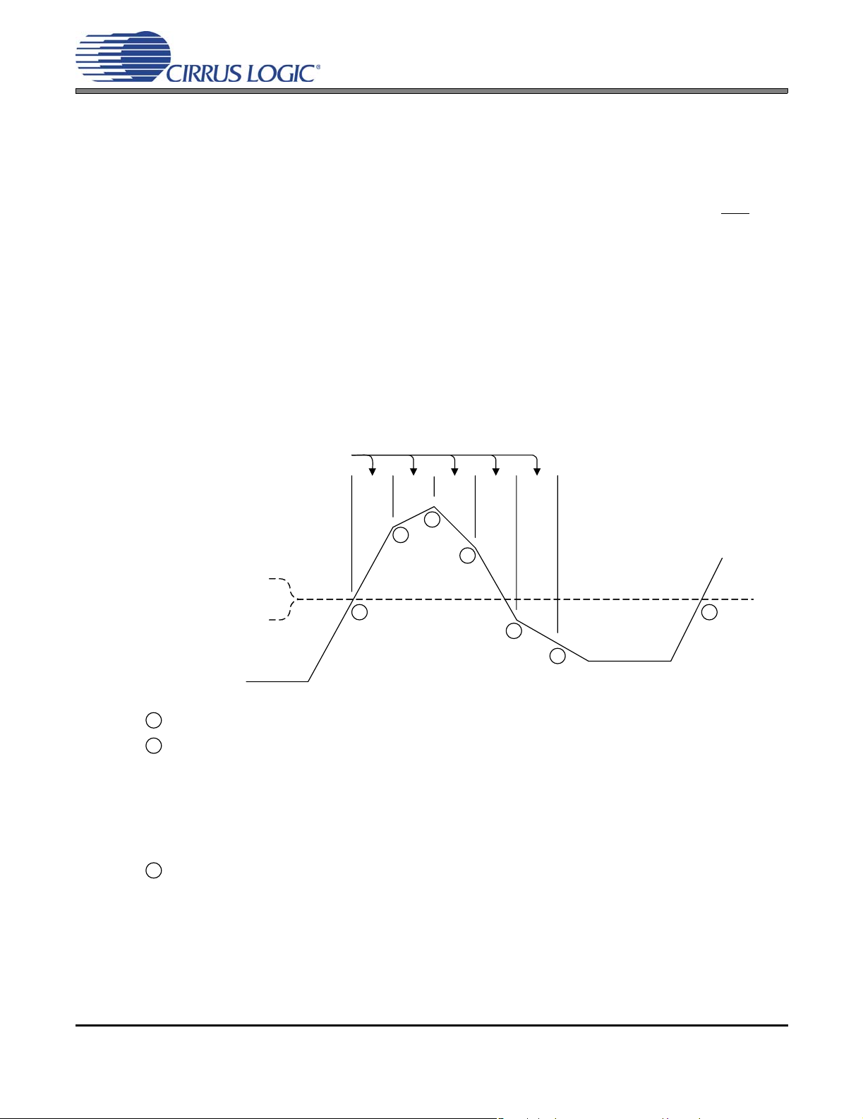
CS4525
6.1.4.12 Thermal Foldback
The CS4525 implements comprehensive thermal foldback features to guard against damaging thermal
overload conditions. Thermal foldback is similar to the thermal limiting described on page 39 in that both
features attenuate the output signal in response to thermal warnings conditions; however, thermal foldback will attenuate as a function of how long thermal warning has been active whereas thermal limiter
always limits by a constant amount. Also, the thermal foldback feature will deactivate once the thermal
warning condition ceases while the thermal limiter will remain active once triggered until the RST
driven low.
The thermal foldback algorithm begins limiting the volume of the digital audio input to the amplifier stage
as the junction temperatures rise above the maximum safe o perating range specified by the thermal warning trigger point listed in the PWM Power Output Characteristics table on page 20. This effectively limits
the output power capability of the device, thereby allowing the temperature to reduce to acceptable levels
without fully interrupting operation. As the device cools, the applied attenuation is gradually released until
a new thermal equilibrium is reached or all applied attenuation has been released thereby allowing the
device to again achieve its full output power capability.
Attenuation applied due to thermal foldback reduces the audio output level in a linear manner. Figure 18
below demonstrates the foldback process.
Foldback Attack Delay
AttackDly[1:0]
t
t
delay
delaytdelaytdelaytdelay
pin is
2
2
2
Thermal Warning
Threshold
When the junction temperature crosses the thermal warning threshold, the foldback attack delay timer is started.
1
When the foldback attack delay timer reaches t
2
temperature is above the thermal warning threshold, the output volume level is lowered by 0.5 dB and the foldback
attack timer is restarted.
The junction temperature is checked after each foldback attack timer timeout, and if necessary, the output volume level
is lowered accordingly.
If the junction temperature is found to be below the thermal warning threshold, the foldback attack timer is restarted
once again, but the output volume level is not altered. The foldback algorithm then proceeds to step 3.
The junction temperature is checked once again after the next foldback attack timer timeout. If it has remained below the
3
thermal warning threshold since the last check, the device will begin to release any attenuation applied as a result of the
foldback event. Setting the LockAdj bit will prevent the device from removing the applied attenuation when the thermal
overload condition has cleared.
1
2
3
seconds, the junction temperature is checked. If the junction
delay
1
If the junction temperature crosses the thermal warning threshold again, the foldback algorithm will once again enter
step 1.
Figure 18. Foldback Process
40 DS726PP2
Page 41

CS4525
The AttackDly[1:0] bits in the Foldback Cfg register allow the foldb ack attack delay time out period to be
adjusted from approximately 0.5 seconds to approximately 2.0 seconds. The maximum attenuation applied by the thermal foldback algorithm can be restricted to -30 dB by setting the EnFloor bit in the same
register.
The foldback adjustment lock feature causes the attenuation applied by the foldback algorithm to be maintained after the foldback condition has subsided. The applied attenuation will continue to be applied until
the master volume or all active channel volume controls are lowered below the foldback attenuation level,
or until a subsequent foldback condition occurs causing the applied attenuation to be lowered further. If
the foldback algorithm applies attenuation while this feature is enabled, when the feature is su bsequently
disabled, the applied attenuation will be gradually released as long as the temperature remains within the
safe operating range. This foldback lock adjustment feature is enabled by the LockAdj bit in the
Foldback Cfg register.
Thermal warnings will only affect the foldback algorithm and cause attenuation to be applied when enabled by the EnTherm bit in the Foldback Cfg register.
The CS4525 can be configured to accept an external thermal warning indicator input. When in this configuration, an active input signal indicates that a ther mal warning thresh old has been exceeded. If therm al
foldback is enabled, the foldback algorithm will respond as described above making no distinction between an internal or external thermal warning condition. See “External Warning Input Port” on page 44 for
more information.
Referenced Control Register Location
EnTherm ............................. “Enable Thermal Foldback (EnTherm)” on page 74
AttackDly[1:0]...................... “Foldback Attack Delay (AttackDly[1:0])” on page 75
EnFloor................................ “Enable Foldback Floor (EnFloor)” on page 75
LockAdj ............................... “Lock Foldback Adjust (LockAdj)” on page 74
6.1.4.13 2-Way Crossover & Sensitivity Control
The CS4525 implements a dedicated stereo 24 dB/octave Linkwitz-Riley crossover filter with adjustable
cross-over frequency and sensitivity control to facilitate 2-way speaker configurations. The filter’s highpass output can be used to drive the tweeter, and its low-pass output is used can be drive the midrange/woofer. The sensitivity control is included to adjust the leve l of the hig h-pass and lo w-pass o utputs
to compensate for differences in the tweeter and mid-range/woofer sensitivity.
The two-way crossover is implemented with one of two preset internal filter sets. One set is optimized for
a 32 kHz sample rate, and the other is optimized for 44.1 kHz, 48 kHz, and 96 kHz sample rates. The
CS4525 automatically detects the input sample rate and chooses the appropriate filter set to apply. The
available cross-over frequencies are shown in Table 5 below and are configured with the 2WayFreq[2:0]
bits in the Volume Cfg register.
Note that the corner frequency of each filter set scales linearly with the input sample rate.
When the internal ADC is used as the serial audio data sour ce, the input sample rate is nominally 48 kHz
and the corresponding shelving frequency corners are available.
Input Sample Rate
32 kHz 44.1 kHz 48 kHz, 96 kHz
X-Over Freq 0 2.0 kHz 1.92 kHz 2.09 kHz
X-Over Freq 1 2.2 kHz 2.11 kHz 2.30 kHz
X-Over Freq 2 2.4 kHz 2.30 kHz 2.50 kHz
X-Over Freq 3 2.6 kHz 2.49 kHz 2.71 kHz
X-Over Freq 4 2.8 kHz 2.68 kHz 2.92 kHz
Table 5. 2-Way Cross-Over Frequencies
DS726PP2 41
Page 42

CS4525
Input Sample Rate
32 kHz 44.1 kHz 48 kHz, 96 kHz
X-Over Freq 5 3.0 kHz 2.88 kHz 3.13 kHz
X-Over Freq 6 3.2 kHz 3.07 kHz 3.34 kHz
X-Over Freq 7 3.4 kHz 3.26 kHz 3.55 kHz
Table 5. 2-Way Cross-Over Frequencies
The sensitivity level of the high- and low-pass outputs of the crossovers can be independently adjusted
from 0 dB to -7.5 dB in 0.5 dB increments. The maximum attenuation level of -7.5 dB will compensate for
an approximate 4 dB difference in sound pressure level (SPL) between the tweeter and the midrange/woofer drivers. The sensitivity is adjusted using the HighPass[3:0] and LowPass[3:0] bits in the
Sensitivity register. Note that these bits affect the sensitivity of both channel A and channel B high- and
low-pass outputs.
The 2-way crossover can be enabled by setting the En2Way bit in the Volume Cfg register.
Referenced Control Register Location
En2Way............................... “Enable 2-Way Crossover (En2Way)” on page 81
2WayFreq[2:0]..................... “2-Way Cross-Over Frequency (2WayFreq[2:0])” on page 81
HighPass[3:0]...................... “Channel A and Channel B High-Pass Sensitivity Adjust (HighPass[3:0])” on page 82
LowPass[3:0]....................... “Channel A and Channel B Low-Pass Sensitivity Adjust (LowPass[3:0])” on page 81
42 DS726PP2
Page 43

6.1.5 Auxiliary Serial Output
The CS4525 includes a stereo auxiliary serial output which allows an external device to leverage on its
internal signal processing and routing capabilities. The auxiliary serial output can receive its data from any
of the sources shown in the Digital Signal Flow diagram on page 29.
The supported output data routing configurations are shown in Table 6 below. By default, the serial port
is configured to output channels A and B on the auxiliary output data left and right channels respectively.
LChDSel[1:0] Aux Left Channel Data RChDSel[1:0] Aux Right Channel Data
00 Channel A 00 Channel A
01 Channel B 01 Channel B
10 Sub Channel 10 Sub Channel
11 Channel B X-Over LPF 11 Channel B X-Over HPF
The data output on each chann el of AUX_SDOUT is set by the LChDSel[1:0] and RChDSel[1:0] bits in
the Aux Port Configuration register. The frequencies of AUX_LRCK and AUX_SCLK will vary based upon
the whether the serial input or analog input is being used and the frequency of the system clock for the
CS4525; the nominal values for these clocks are listed in Table 7. The characteristics of AUX_SCLK,
AUX_LRCK, and AUX_SDOUT are described in the AUX Serial Audio I/O Port Switching Specifications
table on page 22.
CS4525
Table 6. Auxiliary Serial Port Data Output
Signal
Applied System Clock from either
SYS_CLK or External Crystal
Frequency of LRCK Input 32kHz, 44.1kHz,
Nominal Frequency of AUX_SCLK
Output
Nominal Frequency of AUX_LRCK
Output
Table 7. Nominal Switching Frequencies of the Auxiliary Serial Output
18.432, 24.576, or 27.000MHz 18.432MHz 24.576MHz 27.000MHz
or 48kHz
Frequency of
SCLK Input
Frequency of
LRCK Input
ADC/SP
(Digital Input Mode)
= 0
ADC/SP = 1
(Analog Input Mode)
96kHz Not Applicable
Frequency of
SCLK Input / 2
Frequency of
LRCK Input / 2
2.304MHz 3.072MHz 3.375MHz
48kHz 48kHz 52.734kHz
The auxiliary port can be enabled using the EnAuxPort bit. When enabled, the port operates as a master
and clocks out data in the format dictated by the AuxI²S/LJ
bit. When disabled, the AUX_LRCK,
AUX_SCLK, and AUX_SDOUT pins continuously drive a logic ‘0’. It should be noted that when the
CS4525 is configured for analog input, the AUX_LRCK, AUX_SCLK, and AUX_SDOUT pins will continuously drive a logic ‘0’ if either the PDnADC bit or PDnAll bit is set.
Referenced Control Register Location
EnAuxPort........................... “Enable Aux Serial Port (EnAuxPort)” on page 72
LChDSel[1:0]....................... “Aux Serial Port Left Channel Data Select (LChDSel[1:0])” on page 73
RChDSel[1:0]......................“Aux Serial Port Right Channel Data Select (RChDSel[1:0])” on page 72
AuxI²S/LJ............................. “Aux/Delay Serial Port Digital Interface Format (AuxI²S/LJ)” on page 72
PDnADC.............................. “Power Down ADC (PDnADC)” on page 88
PDnAll.................................“Power Down (PDnAll)” on page 89
DS726PP2 43
Page 44
6.1.6 Serial Audio Delay & Warning Input Port
The CS4525 includes a configurable delay and warning port to allow easy system integration of external
lip-sync delay devices or warning inputs from external amplifiers. The port can be configured as a serial
audio delay interface, an external warning input port, or disabled by the DlyPortCfg[1:0] bits in the Aux
Config register. When disabled, the DLY_SDOU T and DLY_SDIN/EX_TWR
ance.
Referenced Control Register Location
DlyPortCfg........................... “Delay & Warning Port Configuration (DlyPortCfg[1:0])” on page 72
6.1.6.1 Serial Audio Delay Interface
Video processing and reproduction circuitry in dig ital video display devices can often introduce noticeably
more delay than is introduced by the device’s audio processing and reproduction c ircuitry. This can resu lt
in a phenomenon known as lip-synch delay - a delay present between the video and audio con tent be ing
reproduced.
To help overcome this problem, the CS4525 delay and warning port can be configured as serial audio
delay interface. This interface consists of a serial audio input/output port to facilitate the use of an external
serial audio delay device. The port routes th e serial data from the selected input source (the ADC or the
serial input port) out to an external serial audio delay device, and then back in to the CS4525 internal digital sound processing blocks. The delay serial audio interface signals include DLY_SDOUT and
DLY_SDIN/EX_TWR
DLY_SDOUT pin and input on the DLY_SDIN/EX_TWR
the Aux Config register. Because the delay interface uses the auxiliary port clock signals, the auxiliary serial port must be enabled using the EnAuxPort bit in the Aux Port Configuration register to allow the dela y
interface to operate properly.
and are clocked from AUX_LRCK and AUX_SCLK. The serial data is output on the
CS4525
pins become high-imped-
in the format specified by the AuxI²S/LJ bits in
Referenced Control Register Location
AuxI²S/LJ............................. “Aux/Delay Serial Port Digital Interface Format (AuxI²S/LJ)” on page 72
EnAuxPort........................... “Enable Aux Serial Port (EnAuxPort)” on page 72
6.1.6.2 External Warning Input Port
When implementing external PWM power stage devices with thermal warning indicator outputs, it can be
useful to provide these warning signals as an input to the internal thermal foldback algorithm. This allows
the CS4525 to automatically r espond to the external devices’ thermal warning conditions witho ut completely disrupting the system’s operation.
When configured as an external warning input port, the DLY_SDIN/EX_TWR
warning input to the foldback algorithm and the DLY_SDOUT pin becomes high-impedance.
In order for the foldback algorithm to act on the external the rmal warning input signal, the th ermal foldback
algorithm must be enabled by the EnTherm bit in the Foldback Cfg register. See “Thermal Foldback” on
page 40 for more information.
Referenced Control Register Location
EnTherm ............................. “Enable Thermal Foldback (EnTherm)” on page 74
is an active-low thermal
44 DS726PP2
Page 45

6.1.7 Powered PWM Outputs
The CS4525’s 3 internal modulators can be used to generate multiple powered PWM output configurations to enable a wide variety of system implementations. The CS4525 also implements PWM Popguard
to minimize output transients in half-bridge configurations.
6.1.7.1 Output Channel Configurations
Three PWM power output configurations are supported as shown in Table 8 below. The configurations
support stereo full-bridge, stereo half-bridge with full-bridge sub, and mono parallel full-bridge output.
OutputCfg[1:0] Power Configuration Output Signal Output Pin(s)
00 2 Ch. Full-Bridge Channel 1 +
01 2 Ch. Half-Bridge
1 Ch. Full-Bridge
10 1 Ch. Parallel Full-Bridge Channel 1 +
Channel 1 -
Channel 2 +
Channel 2 -
Channel 1 +
+
Channel 2 +
Sub Channel +
Sub Channel -
Channel 1 -
Table 8. PWM Power Output Configurations
CS4525
OUT1
OUT2
OUT3
OUT4
OUT1
OUT2
OUT3
OUT4
OUT1, OUT2
OUT3, OUT4
The configurations are selected by the OutputCfg[1:0] bits in the Output Cfg register and must only be
changed when the device is in power-down mode (the PDnAll bit is set). Any attempt to write the OutputCfg[1:0] bits while the device is powered-up will be ignored.
It should be noted that signals on channels 1, 2 and the sub channel are dependent upon the digital sound
processing blocks being used. For instance, if the 2-way cross over is enabled, chann el 1 and 2 contain
the 2-way crossover channel A high- and low-pass outputs respectively. For more information, see the
Digital Sound Processing section and Figure 14 on page 29.
Referenced Control Register Location
OutputCfg[1:0]..................... “Output Configuration (OutputCfg[1:0])” on page 73
PDnAll.................................“Power Down (PDnAll)” on page 89
6.1.7.2 PWM Popguard Transient Control
The CS4525 uses Popguard technology to minimize the effects of powe r-up and power-down output tr ansients commonly produced by half-bridge, single supply amplifiers implemented with external DC-blocking capacitors connected in series with the au dio out pu ts .
PWM Popguard operates by linearly ramping the PWM power outputs up to and down from their bias point
of VP/2 when a channel is powered up and down respectively using the PDnOutX or PDnAll bits. This
DS726PP2 45
Page 46

CS4525
gradual voltage ramp minimizes output transients while the DC blocking capacitor is charged and discharged. The Popguard has no effect on the PWM_SIG outputs nor the auxiliary serial output.
+8V to +18V
0.033 uF
VP
P
A
C
OUT1
_
P
M
A
R
OUT2
Half-
bridge
Filter
Half-
bridge
Filter
Left
Speaker
Right
Speaker
CS4525
OUT3
OUT4
Figure 19. Popguard Connection Diagram
PWM Popguard is disabled by default; to enable it, the RmpSpd[1:0] register must be set to any value
other than 11. PWM Popguard sh ould only be used for ha s when the power outp uts are configured for
stereo half-bridge with full-bridge sub per Section 6.1.7.1. The RAMP_CAP pin must be connected to the
VP supply through a 0.033 µF capacitor whenever PWM Popguard is enabled, as shown in Figure 19.
VP Voltage
12 V 2.16 second s 2.20 seconds 2.20 seconds Instant (No Ramp)
15 V 1.74 second s 1.76 seconds 1.78 seconds Instant (No Ramp)
18 V 1.40 second s 1.42 seconds 1.44 seconds Instant (No Ramp)
RmpSpd[1:0] = 00 RmpSpd[1:0] = 01 RmpSpd[1:0] = 10 RmpSpd[1:0] = 11
Full-
bridge
Filter
Subwoofer
Typical Ramp Up Times
Table 9. Typical Ramp Times for Various VP Voltages
PWM Popguard’s output ramp time will vary depending on the voltage applied to VP and the value of the
RmpSpd[1:0] bits; typical ramp times are listed in Table 9. All output channels are affected by the
RmpSpeed[1:0] bits, and PWM Popguard is disabled by default.
Referenced Control Register Location
RmpSpeed[1:0]...................“Ramp Speed (RmpSpd[1:0])” on page 75
PDnAll.................................“Power Down (PDnAll)” on page 89
PDnOutX............................. “Power Down PWM Power Output X (PDnOutX)” on page 88
6.1.8 Logic-Level PWM Outputs
The CS4525 has two configurable logic-level PWM outp uts, PWM_SIG1 and PWM_SIG2. These ou tputs
can be used as either digital input to an external PWM amplifier such as the CS4412, or as an analog
input to a headphone amplifier or a line-out amplifier.
To eliminate power-up pops when used to supply an external PWM amplifier, the CS4525 implements the
same click-free start-up function on the PWM_SIG outputs as it does for its own powered PWM outputs.
This function can only be utilized if the PWM amplifier has an initial transition delay feature, such as the
CS4412A. To eliminate power-up and power-down pops when used to supply an analog output circuit,
the PWM_SIG outputs support a high-impedance state that is controlled by the HiZPSig
46 DS726PP2
bit in the
Page 47

CS4525
EQ Config register. This bit is active-low and cleared by default. To use the PWM_SIG outputs, the HiZPSig bit must be set to enable the PWM_SIG output drivers.
6.1.8.1 R ecommended PWM_SIG Power-Up Sequence for an External PWM
Amplifier
1. Engage the reset/power-down feature of the external PWM amplifier.
2. Set the PDnAll bit in the Power Ctrl register to stop the PWM modulators if it is not already set.
3. Configure the PWM_SIG outputs as desired via the PWMDSel[1:0] bits in the Output Cfg register.
4. Set the HiZPSig
5. Disengage the reset/power-d own feature of the external PWM amplifier if it has an initial transition
delay feature, such as the CS4412A.
WARNING:Releasing the external amplifier from reset/power-down be fore PWM modulators have started
will cause a DC output on the speakers unless the external amplifier has an initial transition delay feature.
6. Clear the PDnAll bit in the Power Ctrl register to start the PWM modulators.
7. Disengage the reset/power- down featur e of the ext ernal PWM amplifier if it has not been yet disengaged.
6.1.8.2 R ecommended PWM_SIG Power-Down Sequence for an External PWM
Amplifier
bit in the EQ Config register to activate the PWM_SIG output drivers.
1. Mute the PWM_SIG outputs to a 50% duty-cycle by either setting Master Volume to 1111 1111h
(Master Mute) or through use of the HP_DETECT/MUTE input pin as described in the Headphone
Detection & Hardware Mute Input section on page 51.
2. Engage the reset/power-down feature of the external PWM amplifier.
3. Set the PDnAll bit in the Power Ctrl register to disable the PWM modulators and set the PWM_SIG
outputs to a drive a logic ‘0’.
4. Power down the remainder of the system (if ap plic ab le ).
DS726PP2 47
Page 48

CS4525
6.1.8.3 Recommended PWM_SIG Power-Up Sequence for Headphone & Line-
Out
1. Set the PDnAll bit in the Power Ctrl register to stop the PWM modulators if it is not already set.
2. Configure the PWM_SIG outputs as desired via th e PWMDSel[1:0] bits in the Output Cfg register.
3. Clear the PDnAll bit in the Power Ctrl register to start the PWM modulators.
4. Wait 500 ms to allow the internal sample rate converters to achieve lock.
5. Set the HiZPSig
6.1.8.4 Recommended PWM_SIG Power-Down Sequence for Headphone &
Line-Out
1. Mute the PWM_SIG outputs to a 50% duty-cycle by either setting Master Volume to 1111 1111h
(Master Mute) or through use of the HP_DETECT/MUTE input pin as described in the Headphone
Detection & Hardware Mute Input section on page 51.
2. Clear the HiZPSig
ance state.
3. Power down the remainder of the system (if applicable).
Referenced Control Register Location
PDnAll.................................“Power Down (PDnAll)” on page 89
HiZPSig
PWMDSel[1:0]..................... “PWM Signals Output Data Select (PWMDSel[1:0])” on page 73
Master Volume.................... “Master Volume Control (MVol[7:0])” on page 82
...............................“Hi-Z PWM_SIG Outputs (HiZPSig)” on page 79
bit in the EQ Co nfig regist er to act ivat e th e PWM_SI G ou tp ut s.
bit in the EQ Config register to put the PWM_SIG output drivers in a high-imped-
48 DS726PP2
Page 49

CS4525
6.1.8.5 P WM_SIG Logic-Level Output Configurations
Four channel mapping output configurations are supported for the PWM_SIG output pins as shown in
Table 10 below. The configurations support stereo, channel 1 with sub, and channel 2 with sub applica-
tions. When disabled, the PWM_SIG pins will continuously drive a logic ‘0’ if the HiZPSig
be held in a high-impedance state if th e H iZP Sig
bit is clear. The configurations are selected by the PWMDSel[1:0] bits in the Output Cfg register. The PWM_SIG2 can be configured to output the sub channel
even if the Bass Manager is not enabled; however, its signal will be muted unless the Bass Manager is
enabled by the BassMgr[2:0] bits. It should be noted that the HiZPSig
bit must be set to enable the
PWM_SIG output drivers.
PWMDSel[1:0] PWM_SIG1 PWM_SIG2
00 Disabled. Disabled.
01 Channel 1 Channel 2
10 Channel 1 Sub Channel
11 Channel 2 Sub Channel
Table 10. PWM Logic-Level Output Configurations
To allow stereo headphone operation when the PWM logic-level outpu ts are mapped in a non-stereo output configuration, if the HP_DETECT/MUTE pin is configured for headphone detection (the HP/Mute
is set), the PWM logic-level output mapping can be affected by the active state of the he adphone detection
input signal. See the Headphone Detection & Hardware Mute Input se ction on page51 for more information.
bit is set and will
bit
It should be noted that signal on channels 1, 2, and the sub channel are dependent upon the digital soun d
processing blocks being used. For instance, if the 2-way cross over is enabled, chann el 1 and 2 contain
the 2-way crossover channel A high- and low-pass outputs respectively. For more information, see the
Digital Sound Processing section and Figure 14 on page 29.
Referenced Control Register Location
PWMDSel[1:0]..................... “PWM Signals Output Data Select (PWMDSel[1:0])” on page 73
HiZPSig
HP/Mute
BassMgr[2:0]....................... “Bass Cross-Over Frequency (BassMgr[2:0])” on page 79
...............................“Hi-Z PWM_SIG Outputs (HiZPSig)” on page 79
..............................“HP_Detect/Mute Pin Mode (HP/Mute)” on page 70
DS726PP2 49
Page 50

6.1.9 PWM Modulator Configuration
The CS4525 PWM modulators support flexible configuration options designed to simplify system integration. Delays may be inserted between the switching edges on adjacent channels to manage noise, and
the PWM switching frequency can be easily modified to eliminate interference with AM tuners.
6.1.9.1 PWM Channel Delay
The CS4525 includes a PWM output signal delay mechanism. This mechanism allows the PWM switching
edges to be offset between channels as a method of managing switching noise and reducing radiated
emissions.
The OutputDly[3:0] bits in the Output Cfg register are used to adjust the channel delay amount from
0 to 15 SYS_CLK or crystal input clock cycles, whichever is used as the input clock source. The absolute
delay time is calculated by multiplying the setting of the OutputDly[3:0] bits by the period of the input clock
source. By default, no delay is inserted.
When the power outputs are configured for 2-channel full- bridge operation, the OUT3/OUT4 signal p air is
delayed from the OUT1/OUT2 signal pair by the delay amount as shown in Figure 20.
OUT1
CS4525
OUT2
tch
dly
OUT3
OUT4
Figure 20. 2-Channel Full-Bridge PWM Output Delay
When the power outputs are configured for 3-channel (2-channel half-bridge and 1-channel full-bridge)
operation, OUT2 is delayed from OUT1 by the delay amount, and the OUT3/OUT4 pair is delayed from
OUT2 by the delay amount as shown in Figure 21.
OUT1
tch
dly
OUT2
tch
dly
OUT3
OUT4
Figure 21. 3-Channel PWM Output Delay
The OutputDly[3:0] bits can only be changed when all modulators and associated logic are in the powerdown state by setting the PDnAll bit. Attempts to write these bits while the PDnAll bit is cleared will be
ignored.
Referenced Control Register Location
OutputDly[3:0].....................“Channel Delay Settings (OutputDly[3:0])” on page 73
50 DS726PP2
Page 51

CS4525
6.1.9.2 PWM AM Frequency Shift
When using a PWM amplifier in a system containing an AM tuner, it is possible that the PWM switch rate
conflicts with the desired tuning frequency of the AM tuner . To overcome this effect, the CS4525 includes
a PWM switch rate shift feature.
The feature adjusts the PWM switching frequency and quantization levels to remove interference when
the desired tuning frequency of an AM tuner is positioned near a harmonic of the PWM switching rate.
This feature is enabled by setting the FreqShift bit in the Clock Config register. When this feature is enabled, the output switch rate is lowered and the qua ntization levels are incre ased as shown in Table 11
below.
Supplied XTAL or
SYS_CLK Frequency PWM Switch Rate Quantization Levels
18.432 MHz 329.143 kHz 56
24.576 MHz 341.300 kHz 72
27.000 MHz 375 kHz 72
Table 11. PWM Output Switching Rates and Quantization Levels
The nominal PWM switching frequencies and quantization levels are discussed in “PWM Modulators and
Sample Rate Converters” on page 58.
Referenced Control Register Location
FreqShift.............................. “AM Frequency Shifting (FreqShift)” on page 70
6.1.10 Headphone Detection & Hardware Mute Input
The CS4525 includes a configurable HP_DETECT/MUTE input pin which can be used as a hardware
mute input or a headphone detection input. The function of this pin is set by the HP/Mute
Config register.
When configured as a mute input pin, all PWM modulators and the AUX_SDOUT signal will be placed in
a mute state when the pin is active.
When configured as a headphone detect input pin and the HP_DETECT/MUTE input is active, the
PWM_SIG1 and PWM_SIG2 output pins can output audio from ch annel 1 and channel 2 respectively regardless of the setting of the PWMDSel[1:0] bits. The OUT1 - OUT4 PWM driver outputs will mute by outputting a non-modulated 50% duty cycle signal. While the headphone detect input signal is active, the
channel mixing, 2-way crossover, and bass management features will all be disabled regardless of the
settings of the LChMix[1:0], En2Way, and BassMgr[2:0] bits, respectively . It should be noted that the ri ght
channel’s channel mixing is not affected by the headphone detection input signal and will always output
as dictated by the RChMix[1:0] bits. See “Channel Mixer” on page 30, “2-Way Crossover & Sensitivit y
Control” on page 41, and “Bass Management” on page 35 for more information.
When configured as a headphone detect input pin and the HP_DETECT/MUTE input is inactive, the
OUT1 - OUT4 driver outputs will output audio according to the channel mixer and bass manager bits’ settings, and the PWM_SIG output pins will mute by outputting a non-modulated 50% duty cycle.
bit in the Clock
DS726PP2 51
Page 52

CS4525
HiZPSig
Setting
0 X X X X High Impedance High Impedance
1
*Signals denoted with one asterisk do not have Bass Manager, 2-Way Crossover, or Channel Mix applied.
HP/Mute
Setting
X X X 00 (Disabled) Driven Low Driven Low
(Mute
Mode)
(Head-
phone
Mode)
**Signals denoted with two asterisks do not have Bass Manager or 2-Way Crossover applied.
0
1
HP_DETECT
/MUTE Input
Not Active
Active X 01, 10, or 11 Mute Mute
Not Active X 01, 10, or 11 Mute Mute
Active
BassMgr [2:0]
Setting
000
(Disabled)
001 through 111
000
(Disabled)
001 through 111 01, 10, or 11 Channel 1* Channel 2**
PWMDSel [1:0]
Setting
01 Channel 1 Channel 2
10 Channel 1 Mute
11 Channel 2 M ute
01 Channel 1 Channel 2
10 Channel 1 Sub Channel
11 Channel 2 Sub Channel
01 Channel 1* Channel 2**
10 Channel 1* Mute
11 Channel 2** Mute
PWM_SIG1
Output
PWM_SIG2
Output
Table 12. Output of PWM_SIG Outputs
Table 12 describes the exact output of the PWM_SIG output pins based on the input to the
HP_DETECT/MUTE pin and the settings of the HiZPSig
, HP/Mute, BassMgr[2:0], and PWMDSel[ 1:0]
bits. In all configurations, the active logic input level is determined by the HP/MutePol bit.
Referenced Control Register Location
HP/Mute..............................“HP_Detect/Mute Pin Mode (HP/Mute)” on page 70
HP/MutePol......................... “HP_Detect/Mute Pin Active Logic Level (HP/MutePol)” on page 70
PWMDSel[1:0]..................... “PWM Signals Output Data Select (PWMDSel[1:0])” on page 73
LChMix[1:0]......................... “Left Channel Mixer (LChMix[1:0])” on page 76
RChMix[1:0] ........................ “Right Channel Mixer (RChMix[1:0])” on page 76
En2Way............................... “Enable 2-Way Crossover (En2Way)” on page 81
BassMgr[2:0]....................... “Bass Cross-Over Frequency (BassMgr[2:0])” on page 79
HiZPSig
...............................“Hi-Z PWM_SIG Outputs (HiZPSig)” on page 79
52 DS726PP2
Page 53

6.1.11 Interrupt Reporting
The CS4525 has comprehensive interrupt reporting capabilities. Many conditions including SRC lock,
ADC overflow, digital data path overflow, and amplifier errors can cause a n interrupt.
CS4525
The INT
output pin is intended to drive an interrupt input pin on a host microcontroller. The INT pin is an
open-drain active-low output and requires an external pull-up for proper operation.
If an interrupt source is un-masked, its occurrence will cause the interrupt output pin to become active. To
enhance flexibility, each interrupt source may be masked such that its occurrence does not cause the interrupt output pin to become ac tive. This m asking f unction is accomplis hed by clearing an interr upt’s respective mask bit located in the 4 LSB’s of the Interrupt register.
When a specific interrupt condition occurs, it’s re spective bit located in the 4 MSB’s of the Interrupt regi ster
will be set to indicate that a change has occurred fo r the associated interrupt type. When the interrupt r egister is read, the contents of the 4 MSB’s will be cleared. The Int Status register may then be read to determine the current state of the interrupt source.
For specific information regarding interrupt types and reporting, see the In terrup t, Int Status and Amp Error register descriptions.
Referenced Control Register Location
Interrupt Register ................ “Interrupt (Address 60h)” on page 89
Int Status Register............... “Interrupt Status (Address 61h) - Read Only” on page 92
Amp Error Register ............. “Amplifier Error Status (Address 62h) - Read Only” on page 93
6.1.12 Automatic Power Stage Shut-Down
To prevent permanent damage, the CS4525 will automatically shut down its internal PWM power output
stages when a thermal error, PWM power output over-current er ror, or VP under-voltage condition occurs.
In the shut-down state, all digital functions of the device will operate as normal, however the PWM power
output pins become high-impedance.
The levels of the over-current er ror, thermal error, and VP un der-voltage trigger points ar e listed in the
PWM Power Output Characteristics table on page 20. Automatic shut-down will occur whenever any of
these preset thresholds are crossed.
Once in the shut-down state, each powered PWM outputs will remain as high-impedance and will not re-
sume normal operation until either the PDnAll bit or the PDnOutX bit for the channel in error is set and
then cleared.
If the AutoRetry bit is set, the CS4525 will attempt to automatically resume power output operation after
an over-current error is encountered and before entering the shut-down state. With the AutoRetry function
enabled, the CS4525 will place the PWM power outputs in a high-impedance state upon the sensing of
an over-current condition, wait approximately 85 ms, and then re-engage the power outputs in an attempt
to resume normal operation. If another over-current condition is immediately detected, the PWM power
outputs will again be placed in a high-impedance state before retrying to resume normal operation a second time. It will continue this sequence for a maximum of five attempts. After the fifth unsuccessful attempt, the outputs will remain in a high-impedance state until the PDnAll bit is set and then cleared.
Referenced Control Register Location
AutoRetry............................“Automatic Power Stage Retry (AutoRetry)” on page 88
PDnAll.................................“Power Down (PDnAll)” on page 89
PDnOutX............................. “Power Down PWM Power Output X (PDnOutX)” on page 88
DS726PP2 53
Page 54

6.2 Hardware Mode
A limited feature set is available when the CS4525 powers up in hardwa re mode. The available features are
described in the following sections. All device configuration is achieved via hardware control input pins.
6.2.1 System Clocking
In hardware mode, the CS4525 must be clocked by a stable external clock source input on the SYS_CLK
pin. This input clock is used to synchro nize the input serial audio signals with the internal clock domain
and to clock the internal digital processing, sample-rate converter, and PWM modulators. It is also used
to determine the sample rate of the serial audio input signals in order to automatically configure the various internal filter coefficients.
To ensure proper operation, the CS4525 must be informed of the nominal frequency of the supplied
SYS_CLK signal via the ClkFreq[1:0] hardware control pins. These pins must be set to the appropriate
level before the RST
indicated by the states of the ClkFreq[1:0] pins are shown in Table 13 below. See the SYS_CLK Switching
Specifications table on page 23 for complete input frequency range specifications.
ClkFreq1 ClkFreq0 Nominal SYS_CLK Frequency
Low Low 18.432 MHz
Low High 24.576 MHz
High Low 27.000 MHz
High High Reserved
CS4525
signal is released to initiate a power-up sequence. The nominal clock frequencies
Table 13. SYS_CLOCK Frequency Selection
WARNING: The SYS_CLK signal must never be removed or stopped while the RST
of the power output stages are connected to a load. Doing so may result in permanent damage to the
CS4525 and connected transducers.
Figure 22 below demonstrates a typical clocking configuration using the SYS_CLK input.
Clock
Figure 22. Typical SYS_CLK Input Clocking Configuration
6.2.2 Power-Up and Power-Down
The CS4525 will remain in a completely powered-down state until the RST pin is brought high.
6.2.2.1 Recommended Power-Up Sequence
1. Hold RST low until the power supplies and the input SYS_CLK signal are stable.
2. Bring RST
Hardware mode will be entered after approximately 10 ms.
high.
Clock_In
DSP
Reset_Out
RST
SYS_CLK
CS4525
pin is high and any
XTI
XTO
54 DS726PP2
Page 55

6.2.2.2 R ecommended Power-Down Sequence
1. Bring MUTE low to mute the device’s outputs and minimize audible pops.
2. Bring RST
low to halt the operation of the device.
The device’s power consumption will be brought to an absolute minimum.
3. Remove power.
6.2.3 Input Source Selection
The CS4525 can accept analog or digital audio input signals. Digital audio input signals are supplied
through the serial audio input port as outlined in “Ser ial Audio In terfaces” o n page62. Analog audio input
signals are supplied through the internal ADC as outlin ed in “Analog Inputs” on p age 61. The input source
is selected by the ADC/SP
ing any audible pops or clicks.
ADC/SP Selected Input Source
Low Digital Audio Inputs (Serial Port)
High Analog Audio Inputs (ADC)
In hardware mode, the serial audio input port supports both I²S and left-justified formats. The serial audi o
interface format is selected by the I2S/LJ
pin as shown in Table 14 below and can be changed at any time without caus-
CS4525
Table 14. Input Source Selection
pin as shown in Table 15 below.
I2S/LJ Selected Serial Audio Interface Format
Low Left-Justified
High I²S
6.2.4 PWM Channel Delay
In hardware mode, the CS4525 offsets the PWM switching edges between channels as a method of managing switching noise and reducing radiated emissions.
The OUT3/OUT4 signal pair is delayed from the OUT1/OUT2 signal pair by 4 SYS_CLK cycles as shown
in Figure 23 below. The absolute delay time is calculated by multiplying the period SYS_CLK by 4.
OUT1
OUT2
OUT3
OUT4
Table 15. Serial Audio Interface Format Selection
4 x T
SYS_CLK
Figure 23. Hardware Mode PWM Output Delay
DS726PP2 55
Page 56

6.2.5 Digital Signal Flow
In hardware mode, the CS4525 operates as a 2-channel full-bridge PWM amplifier with analog or digital
inputs. Both the PWM outputs and the auxiliary serial outputs are unavailable in hardware mode. To protect against over-temperature conditions, thermal foldback is included for the internal power stages.
The digital signal flow is shown in Figure 24 below.
MUTE
ADC/SP
Stereo
Analog In
Serial Audio
Clocks & Data
I²S/LJ
Multi-Bit
ΔΣ ADC
Serial Audio
Input P ort
CS4525
+3dB
High-Pass
+3dB
Thermal Foldback
Sample
Rate
Converter
Mute
Sample
Rate
Converter
PWM
Modulator
PWM
Modulator
Gate
Drive
Gate
Drive
Gate
Drive
Gate
Drive
Power
Stage
Power
Stage
Power
Stage
Power
Stage
Left
Full-Bridge
Amplifier
Output
Right
Full-Bridge
Amplifier
Output
EN_TFB
Thermal Foldback
Temp & Cur r ent
Sense
Figure 24. Hardware Mode Digital Signal Flow
6.2.5.1 High-Pass Filter
The CS4525 includes a high-pass filter at the beginning of the digital signal processing chain to remove
any DC content from the input signal prior to the remaining internal digital signal processing blocks. The
high-pass filter operates by continuously subtracting a measure of the DC offset from the input signal; it
is always enabled.
6.2.5.2 Mute Control
The CS4525 includes a dedicated MUTE input pin. When low, the PWM outputs will output silence as
modulated signal. When high, the selected input source will be presented at the amplifier outputs.
It should be noted that the auto-mute, soft-ramp, an d zero-crossing detection features are active in hardware mode.
6.2.5.3 Warning and Error Reporting
The CS4525 is capable of reporting various error and warning conditions on its TWR, ERROC, and ERRUVTE pins.
TWR
ERROC
ERRUVTE
•The TWR
ERRUVTE
• The ERROC
pin indicates the presence of a thermal warning condition. When active concurrently with the
pin, indicates a thermal error condition.
pin indicates the presence of an over-current condition on one or both of the output chan-
nels.
• The ERRUVTE
with the TWR
pin indicates the presence of a VP undervoltage condition. When active concurrently
pin, indicates a thermal error condition.
The trigger point for each warning and error condition is defined in the PWM Power Output Characteristics
table on page 20. Each pin implements an active-low open-drain driver and requires an external pull-up
for proper operation.
56 DS726PP2
Page 57

6.2.6 Thermal Foldback
In hardware mode, the CS4525 implements a thermal foldback feature to guard aga inst damaging thermal
overload conditions. The thermal foldback feature begins limiting the volume of the digital audio input to
the amplifier stage as the junction temperatures rise above the maximum safe operating range specified
by the thermal warning trigger point listed in the PWM Power Output Characteristics table on page 20.
This effectively limits the output power capability of the device, thereby allowing the temperature to reduce
to acceptable levels without fully interrupting operation. As th e device cools, the applied attenuation is
gradually released until a new thermal equilibrium is reach ed or all applied atte nuation has been released
thereby allowing the device to again achieve its full output power capability.
Attenuation applied due to thermal foldback reduces the audio output level in a linear manner. Figure 18
below demonstrates the foldback process.
Foldback Attack Delay
Approximately 2 sec.
Thermal Warning
Threshold
CS4525
t
1
delay
t
delaytdelaytdelaytdelay
2
2
2
2
1
3
When the junction temperature crosses the thermal warning threshold, the foldback attack delay timer is started.
1
When the foldback attack delay timer reaches t
2
thermal warning threshold, the output volume level is lowered by 0.5 dB and the foldback attac k timer is restarted.
The junction temperature is checked after each foldback attack timer timeout, and if necessary, the output volume
level is lowered accordingly.
If the junction temperature is found to be below the thermal warning threshold, the foldback attack timer is
restarted once again, but the output volume level is not altered. The foldback algorithm then proceeds to step 3.
The junction temperature is checked once again after the next foldback attack timer timeout. If is has remained
3
below the thermal warning threshold since the last check, the device wil l begin to release any attenuation applied
as a result of the foldback event.
If the junction temperature crosses the thermal warning threshold again, the foldback algorithm will once again
enter step 1.
seconds, the junction temperature is checked. If it is above the
delay
Figure 25. Foldback Process
Thermal warning conditions will only affect the foldback algorithm and cause attenuation to be applied if
enabled by the EN_TFB pin as shown in Table 16 below.
EN_TFB Selected Thermal Foldback Enable State
Low Thermal foldback disabled.
High Thermal foldback enabled.
Table 16. Thermal Foldback Enable Selection
DS726PP2 57
Page 58

6.2.7 Automatic Power Stage Shut-Down
To protect itself from permanent damage, the CS4525 will automatically shut down its internal PWM power output stages when a thermal error, PWM power output over-current error, or VP under-voltage condition occurs. In the shut-down state, all digital functions of the device will operate as normal, however the
PWM power output pins become high-impedance.
The levels of the over-current error, thermal error, and VP under-voltage trigger points are listed in the
PWM Power Output Characteristics table on page 20. Shut-down will occur automatically whenever the
preset thresholds for thermal error or under-voltage are crossed.
When the over-current threshold is crossed, the CS4525 will attempt to automatically resume power out-
put operation after an over-current error is encountere d and be fore pla cing its PWM power o utputs in the
shut-down state. Upon the detection of an over-current condition, the CS4525 will place the PWM power
outputs in a high-impedance state, wait approximately 85 ms, and then re-engage the power outputs in
an attempt to resume normal operation. If another over-current condition is immediately detected, the
PWM power outputs will again be placed in a high-impedance state before retrying to resume normal operation a second time. It will continue this sequence for a maximum of five attempts. After the fifth unsuccessful attempt, the outputs will remain in the high-impedance shut-down state.
CS4525
Once in the shut-down state, the RST
operation.
signal must be toggled low and then high to resume normal device
6.3 PWM Modulators and Sample Rate Converters
The CS4525 includes three PWM modulators and three corresponding sample rate converters, each
clocked from the external crystal or system clock applied at power-up. All three modulator and sample rate
converter pairs are available in software mode (see Figure 14 on page 29), and two pairs are used in hardware mode (see Figure 24 on page 56).
One of the characteristics of a PWM modulator is that the frequency content of the out-of-band noise generated is dependent on the PWM switching frequency. As the power stage external LC and snubber filter
component values are used to attenuate this out-of b and energy, their comp onent values are also based on
this switching frequency.
To easily accommodate input sample rates ranging from 32 kHz to 96 kHz without requiring the adjustment
of output filter component values, the CS4525 utilizes a sample rate converter (SRC) to keep the PWM
switching frequency fixed regardless of the input sample rate. The SRC operates by upsampling the variable
input sample rate to a fixed output switching rate, typically 384 kHz for most audio applications. Table 17
below shows the PWM output switching rate and quantization levels as a function of the supplied external
crystal or system clock.
Additionally, as the output of the SRC is clocked from a very stable crystal or oscillator, the SRC also allows
the PWM modulator output to be independent of the input serial audio clock jitter. This results in very low
jitter PWM output and higher dynamic range.
Supplied XTAL or
SYS_CLK Frequency PWM Switch Rate Quantization Levels
18.432 MHz 384 kHz 48
24.576 MHz 384 kHz 64
27.000 MHz 421.875 kHz 64
Table 17. PWM Output Switching Rates and Quantization Levels
58 DS726PP2
Page 59

6.4 Output Filters
The filter placed after the PWM outputs can greatly affect the output performance. The filter not only reduces
radiated EMI (snubber filter), but also filters high frequency content from the switching output before going
to the speaker (low-pass LC filter).
6.4.1 Half-Bridge Output Filter
Figure 26 shows the output filter for a half-bridge configuration. The transient-voltage suppression circuit
(snubber circuit) is comprised of a capacitor (680 pF) and a resistor (5.6 Ω, 1/8 W) and should be placed
as close as possible to the corresponding PWM output pin to greatly reduce radiated EMI.
CS4525
VP
C2
+-
C1
OUTx
680 pF
L1
*Diode is Rohm
RB160M-30 or
equivalent
5.6 Ω
Figure 26. Output Filter - Half-Bridge
The inductor, L1, and capacitor, C1, comprise the low-pass filter. Along with the nominal load impedance
of the speaker, these values set the cutoff frequency of the filter. Table 18 shows the component values
for L1 and C1 based on nominal speaker (loa d) impedance for a corner frequency (-3 dB point) of approximately 35 kHz.
Load L1 C1
4 Ω 22 µH 1.0 µF
6 Ω 33 µH 0.68 µF
8 Ω 47 µH 0.47 µF
Table 18. Low-Pass Filter Components - Half-Bridge
C2 is the DC-blocking capacitor. Table 19 shows the component values for C2 based on corner frequency
(-3 dB point) and a nominal speaker (load) impedances of 4 Ω, 6 Ω, and 8 Ω. This capacitor should also
be chosen to have a ripple current rating above the amount of current that will passed through it.
Load Corner Frequency C2
4 Ω 40 Hz 1000 µF
58 Hz 680 µF
120 Hz 330 µF
6 Ω 39 Hz 680 µF
68 Hz 390 µF
120 Hz 220 µF
8 Ω 42 Hz 470 µF
60 Hz 330 µF
110 Hz 180 µF
Table 19. DC-Blocking Capacitors Values - Half-Bridge
DS726PP2 59
Page 60
6.4.2 Full-Bridge Output Filter (Stereo or Parallel)
Figure 27 shows the output filter for a full-bridge configuration. The transient-voltage suppression circuit
(snubber circuit) is comprised of a capacitor (680 pF) and a resistor (5.6 Ω, 1/8 W) on each output pin and
should be placed as close as possible to the corresponding PWM output pins to greatly reduce radiated
EMI. The inductors, L1, and capacitor, C1, comprise the low-pass filter. Along with the nominal load impedance of the speaker, these values set the cutoff frequency of the filter. Table 20 shows the component
values based on nominal speaker (load) imped ance for a corner frequ ency (-3 dB point) of approximately
35 kHz.
VP
OUTX+
CS4525
L1
680 pF
5.6 Ω
*Diode is Rohm
RB160M-30 or
equivalent
C1
VP
L2
OUTX-
680 pF
5.6 Ω
Figure 27. Output Filter - Full-Bridge
Load L1, L2 C1
4 Ω 10 µH 1.0 µF
6 Ω 15 µH 0.47 µF
8 Ω 22 µH 0.47 µF
Table 20. Low-Pass Filter Components - Full-Bridge
60 DS726PP2
Page 61
6.5 Analog Inputs
Very few components are required to interface between the audio so ur ce an d the CS4 525’s ana log inputs,
AINL and AINR. A single order passive low-pass filter is recommended to prevent high-frequency content
from aliasing into the audio band due to the analog-to-digital conversion process. Also, a DC-blocking capacitor is required as the CS4525’s analog inputs are internally biased to VQ.
The recommended analog input circuit is shown in Figure 28 below will accommodate full-scale input voltages as defined in the Analog Input Characteristics table on page 19. This circuit provides the necessary
high-frequency filtering with a first-order passive low-pass filter that has less than 0.05 dB of attenuation at
24 kHz. It also includes a DC blocking capacitor to accommodate the analog input pins’ bias level.
Left Input
1 µF
CS4525
CS4525
365 Ω
AINL
100 kΩ
1 µF
Right Input
100 kΩ
1800 pF
C0G
365 Ω
AINR
1800 pF
C0G
Figure 28. Recommended Unity Gain Input Filter
To interface 2 V
Figure 29 shows the recommended input circuit for 2 V
input signals with the CS4525’s analog inputs, an external resistor divider is required.
RMS
inputs. It includes a -8.4 dB passive attenuator
RMS
to condition the input signal for the CS4525’s full-scale input voltage, a first-order passive low-pass filter that
has less than 0.05 dB of attenuation at 24 kHz, and a DC blocking capacitor to accommodate for the analog
input pins’ bias level. The passive attenuator network should be placed as close as possible to th e CS4525’s
analog input pins to reduce the potential for noise and signal coupling into the analog input traces.
CS4525
Left Input
8.06 kΩ
5.62 kΩ
1 µF
AINL
100 pF
C0G
Right Input
8.06 kΩ
5.62 kΩ
Figure 29. Recommended 2 V
1 µF
100 pF
C0G
Input Filter
RMS
AINR
It should be noted that the external DC blocking capacitor forms a high-pass filter with the CS4525’s input
impedance. Both filters shown above have less than 0.2 dB attenuation at 20 Hz due to this effect. Increasing the value of this capacitor will lower this high-pass corner frequency, and decreasing it’s value will increase the corner frequency.
DS726PP2 61
Page 62

6.6 Serial Audio Interfaces
The CS4525 interfaces to external digital audio devices via the serial audio input port and the auxiliary/delay
serial ports.
The serial audio input port provides support for I²S, Left-Justified and Right-Justified data formats and operates in slave mode only, with LRCK and SCLK as inputs. The input LRCK signal must be equal to the
sample rate, Fs and must be synchronous to the serial bit clock, SCLK, which is used to sample the data
bits.
The auxiliary/delay serial port (available in software mode only) supports I²S and Left-Justified data formats
and operates in master mode only, with AUX_LRCK and AUX_SCLK as outputs.
Each of the supported formats is described in detail in sections 6.6.1 - 6.6.3 below. Please refer to th e Serial
Audio Input Port Switching Specifications and AUX Serial Audio I/O Port Switching Specifications on
page 21 and page 22 (respectively) for the precise timing and tolerances of each signal.
For additional information, application note AN282 presents a tutorial of the 2-channel serial audio inter face.
AN282 can be downloaded from the Cirrus Logic web site at http://www.cirrus.com.
6.6.1 I²S Data Format
In I²S format, data is received most significant bit first one SCLK delay after the transition of LRCK and is
valid on the rising edge of SCLK. The left ch annel data is presented when LRCK is low; the ri ght channel
data is presented when LRCK is high.
CS4525
LRCK
SCLK
SDIN
MSB MSB
-2 -3 -4 -5
-1
Left Channel
6.6.2 Left-Justified Data Format
In Left-Justified format, data is received most significant bit first on the first SCLK after a LRCK transition
and is valid on the rising edge of SCLK. The left channel data is presented when LRCK is high and the
right channel data is presented when LRCK is low.
LRCK
SCLK
SDIN
MSB LSB MSB LSB
-1 -2 -3 -4 -5
Left Channel
Figure 31. Left-Justified Serial Audio Formats
LSB LSB
+3 +2 +1+5 +4
-1
-2 -3 -4
Figure 30. I²S Serial Audio Formats
+3 +2 +1+5 +4
-1
-2 -3 -4
RightChannel
+3 +2 +1+5 +4
Right Channel
+3 +2 +1+5 +4
62 DS726PP2
Page 63
6.6.3 Right-Justified Data Format
In Right-Justified format, data is received most significant bit first and with the least significant bit presented on the last SCLK before the LRCK transition and is valid on the rising edge of SCLK. For the RightJustified format, the left channe l data is pres ente d when LRCK is high and the right channel data is presented when LRCK is low. 16, 18, 20, and 24 bits per sample are supported.
CS4525
LRCK
SCLK
SDIN
15 14 13 12 11 10
Figure 32. Right-Justified Serial Audio Formats
6.7 Integrated VD Regulator
The CS4525 includes two internal linear regulators, one from the VD supply voltage to pr ovide a fixed 2.5 V
supply to its internal digital blocks, and another from the VD supply voltage to provide a fixed 2.5 V supply
to its internal analog blocks. The LVD pin must be set to indicate the voltage pr esent on the VD pin as shown
in Table 21 below.
VD
Connection
5 V Supply Bypass Capacitors Only Bypass Capacitors Only VD ‘1’ - Default
3.3 V Supply Bypass Capacitors Only Bypass Capacitors Only DGND ‘1’ - Default
2.5 V Supply VD and Bypass Capacitors VD and Bypass Capacitors DGND ‘0’
The output of the digital regulator is presented on the VD_REG pin and may be used to provide an external
device with up to 3mA of current at its nominal output voltage of 2.5 V. The output of the analo g re gula tor
is presented on the VA_REG pin and must only be connected to the bypass capacitors as sh own in the typical connection diagrams.
VD_REG
Connection
Table 21. Power Supply Configuration and Settings
Left Channel
6543210987
VA_REG
Connection
RightChannel
15 14 13 12 11 10
LVD
Connection
6543210987
SelectVD Bit Setting
Software Mode Only
If a nominal supply voltage of 2.5 V is used as the VD supply (see the Recommended Operating Conditions
table on page 18), the VD, VD_REG, and VA_REG pins must all be connected to the VD supply source. In
this configuration, the internal regulators are bypassed and the external supply source is used to directly
drive the internal digital and analog sections.
Referenced Control Register Location
SelectVD.............................“Select VD Level (SelectVD)” on page 88
DS726PP2 63
Page 64

6.8 I²C Control Port Description and Timing
The control port is used to access the registers allowing the CS4525 to be configured for the desired operational modes and formats. The operation of the control port ma y be completely asynchron ous with respect
to the audio sample serial port. However, to avoid potential interference problems, the control port pins
should remain static if no operation is required. The control port operates in I²C Mode, with th e CS4525 acting as a slave device.
SDA is a bidirectional data line. Data is clocked into and out of the part by the clock, SCL. A 47 kΩ pull-up
or pull-down on the AUX_LRCK/AD0 pin will set AD0, the least significant bit of the device address. A pullup to VD will set AD0 to ‘1’ and a pull-down to DGND will set AD0 to ‘0’. The state of AUX_LRCK/AD0 is
sensed, and AD0 is set upon the release of RESET
The signal timings for a read and write cycle are sho wn in Figure 33 and Figure 34. A Start condition is de-
fined as a falling transition of SDA while the clock is high. A Stop condition is a rising transition while the
clock is high. All other transitions of SDA occur while the clock is low. The first byte sent to the CS4525 after
a Start condition consists of a 7 bit device address field and a R/W
upper 6 bits of the 7-bit address field are fixed at 100101. To communicate with a CS4525, the device address field, which is the first byte sent to the CS4525, should match 100101 followed by the setting of AD0.
The eighth bit of the address is the R/W
pointer (MAP) which selects the register to be read or written. If the operation is a re ad, the con tents of the
register pointed to by the MAP will be output. Setting the auto increment bit in MAP allows successive reads
or writes of consecutive registers. Each byte is separated by an acknowledge bit. The ACK bit is outp ut from
the CS4525 after each input byte is read, and is input to the CS4525 from the microcontroller after each
transmitted byte.
bit. If the operation is a write, the next byte is the memory address
CS4525
.
bit (high for a read, low for a write). The
4 5 6 7 24 25
INCR 6 5 4 3 2 1 0 7 6 1 0 7 6 1 0 7 6 1 0
ACK
DATA +1
DATA +n
ACKACKACK
STOP
SCL
SDA
0 1 2 3 8 9 12 16 17 18 19 10 11 13 14 15 27 2826
CHIP ADDRESS (WRITE) MAP BYTE DATA
1 0 0 1 0 1 AD0 0
START
Figure 33. Control Port Timing, I²C Write
16 8 9 12 13 14 15 4 5 6 7 0 1 20 21 22 23 24
STOP
ACK
START
CHIP ADDRESS (READ)
1 0 0 1 0 1 AD0 1
26 27 28
DATA
7 0 7 0 7 0
ACK
DATA +1
ACK
DATA + n
NO
ACK
STOP
SCL
SDA
2 3 10 11 17 18 19 25
CHIP ADDRESS (WRITE)
1 0 0 1 0 1 AD0 0
START
MAP BYTE
INCR 6 5 4 3 2 1 0
ACK
Figure 34. Control Port Timing, I²C Read
Since the read operation can not set the MAP, an aborted write operation is used as a preamble. As shown
in Figure 34, the write operation is aborted after the acknowledge for the MAP byte by sending a stop condition. The following pseudocode illustrates an aborted write operation followed by a read operation.
Send start condition.
Send 100101x0 (device address and write operation).
Receive acknowledge bit.
Send MAP byte, auto increment off.
Receive acknowledge bit.
Send stop condition, aborting write. (Optional.)
Send start condition.
Send 100101x1(device address and read operation).
64 DS726PP2
Page 65

Receive acknowledge bit.
Receive byte, contents of selected register.
Send acknowledge bit.
Send stop condition. (Optional.)
Setting the auto increment bit in the MAP allows successive reads or writes of consecutive registers. Each
byte is separated by an acknowledge bit.
7. PCB LAYOUT CONSIDERATIONS
7.1 Power Supply, Grounding
As with any high-resolution converter, the CS4525 requires careful attention to power supply and grounding
arrangements if its potential performance is to be realized.
Extensive use of power and ground planes, ground plane fill in unused areas and surface mount decoupling
capacitors are recommended. Decoupling capacitors shoul d be as close to the pin s of the CS4525 as possible. The lowest value ceramic capacitor should be closest to the p in and should be mounted on the sam e
side of the board as the C S4525 to minimize ind uctance effects. All signals , especially clocks, shou ld be
kept away from the FILT+ and VQ pins in order to avoid unwanted co upling into th e modulator s. The FILT+
and VQ decoupling capacitors, particularly the 0.1 µF, must be positioned to minimize the electrical path
from FILT+ and AGND. The CRD4525 reference design d emo nstrates the o ptimum layo ut an d power supply arrangements.
CS4525
7.2 QFN Thermal Pad
The CS4525 is available in a compact QFN package. The underside of the QFN package reveals a large
metal pad that serves as a thermal relief to provide for maximum heat dissipation. This pad must mate with
an equally dimensioned copper pad on the PCB and must be electrically connected to ground. A series of
thermal vias should be used to connect this copper pad to one or more larger ground planes on other PCB
layers. The CRD4525 reference design demonstrates the optimum thermal pad and via configuration.
For more information concerning thermal considerations of QFN packages, please refe r to Cirrus Log ic application note AN315.
DS726PP2 65
Page 66

CS4525
8. REGISTER QUICK REFERENCE
This table shows the register names and their associated default values.
Adr Name76543210
01h Clock Config EnSysClk DivSysClk ClkFreq1 ClkFreq0 HP/MutePol HP/Mute PhaseShift FreqShift
page 69 10010000
02h Input Config ADC/SP
page 71 010xx000
03h Aux Config EnAuxPort DlyPortCfg1 DlyPortCfg0 AuxI²S/LJ
page 72 00000100
04h Output Cfg OutputCfg1 OutputCfg0 PWMDSel1 PWMDSel0 OutputDly3 OutputDly2 OutputDly1 OutputDly0
page 73 00000000
05h Foldback Cfg SelectVP EnTherm LockAdj AttackDly1 AttackDly0 EnFloor RmpSpd1 RmpSpd0
page 74 10001011
06h Mixer Config PreScale2 PreScale1 PreScale0 Reserved RChMix1 RChMix0 LChMix1 LChMix0
page 75 00000000
07h Tone Config DeEmph Loudness EnDigHPF TrebFc1 TrebFc0 BassFc1 BassFc0 EnToneCtrl
page 76 00000010
08h Tone Control Treble3 Treble2 Treble1 Treble0 Bass3 Bass2 Bass1 Bass0
page 78 10001000
09h EQ Config Freeze HiZPSig
page 78 00000000
0Ah
BiQuad 1
0Bh MSB-8 ............................................................................................................................. L SB+8
A1 Coeff
0Ch LSB+7 ............................................................................................................................. LSB
0Dh
BiQuad 1
0Eh MSB-8 ............................................................................................................................. L SB+8
A2 Coeff
0Fh LSB+7 ............................................................................................................................. LSB
10h
BiQuad 1
11h MSB-8 ............................................................................................................................. LSB+8
B0 Coeff
12h LSB+7 ............................................................................................................................. LSB
13h
BiQuad 1
14h MSB-8 ............................................................................................................................. LSB+8
B1 Coeff
15h LSB+7 ............................................................................................................................. LSB
16h
BiQuad 1
17h MSB-8 ............................................................................................................................. LSB+8
B2 Coeff
18h LSB+7 ............................................................................................................................. LSB
19h
BiQuad 2
1Ah MSB-8 ............................................................................................................................. L SB+8
A1 Coeff
1Bh LSB+7 ............................................................................................................................. LSB
1Ch
BiQuad 2
1Dh MSB-8 ............................................................................................................................. LSB+8
A2 Coeff
1Eh LSB+7 ............................................................................................................................. LSB
1Fh
BiQuad 2
20h MSB-8 ............................................................................................................................. LSB+8
B0 Coeff
21h LSB+7 ............................................................................................................................. LSB
22h
BiQuad 2
23h MSB-8 ............................................................................................................................. LSB+8
B1 Coeff
24h LSB+7 ............................................................................................................................. LSB
MSB ............................................................................................................................. MSB-7
MSB ............................................................................................................................. MSB-7
MSB ............................................................................................................................. MSB-7
MSB ............................................................................................................................. MSB-7
MSB ............................................................................................................................. MSB-7
MSB ............................................................................................................................. MSB-7
MSB ............................................................................................................................. MSB-7
MSB ............................................................................................................................. MSB-7
MSB ............................................................................................................................. MSB-7
EnAnHPF Reserved SPRate1 SPRate0 DIF2 DIF1 DIF0
RChDSel1 RChDSel0 LChDSel1 LChDSel0
BassMgr2 BassMgr1 BassMgr0 Reserved EnChBPEq EnChAPEq
66 DS726PP2
Page 67

CS4525
Adr Name76543210
25h
BiQuad 2
26h MSB-8 ............................................................................................................................. LSB+8
B2 Coeff
27h LSB+7 ............................................................................................................................. LSB
28h
BiQuad 3
29h MSB-8 ............................................................................................................................. LSB+8
A1 Coeff
2Ah LSB+7 ............................................................................................................................. LSB
2Bh
BiQuad 3
2Ch MSB-8 ............................................................................................................................. LSB+8
A2 Coeff
2Dh LSB+7 ............................................................................................................................. LSB
2Eh
BiQuad 3
2Fh MSB-8 ............................................................................................................................. LSB+8
B0 Coeff
30h LSB+7 ............................................................................................................................. LSB
31h
BiQuad 3
32h MSB-8 ............................................................................................................................. LSB+8
B1 Coeff
33h LSB+7 ............................................................................................................................. LSB
34h
BiQuad 3
35h MSB-8 ............................................................................................................................. LSB+8
B2 Coeff
36h LSB+7 ............................................................................................................................. LSB
37h
BiQuad 4
38h MSB-8 ............................................................................................................................. LSB+8
A1 Coeff
39h LSB+7 ............................................................................................................................. LSB
3Ah
BiQuad 4
3Bh MSB-8 ............................................................................................................................. LSB+8
A2 Coeff
3Ch LSB+7 ............................................................................................................................. LSB
3Dh
BiQuad 4
3Eh MSB-8 ............................................................................................................................. LSB+8
B0 Coeff
3Fh LSB+7 ............................................................................................................................. LSB
40h
BiQuad 4
41h MSB-8 ............................................................................................................................. LSB+8
B1 Coeff
42h LSB+7 ............................................................................................................................. LSB
43h
BiQuad 4
44h MSB-8 ............................................................................................................................. LSB+8
B2 Coeff
45h LSB+7 ............................................................................................................................. LSB
46h
BiQuad 5
47h MSB-8 ............................................................................................................................. LSB+8
A1 Coeff
48h LSB+7 ............................................................................................................................. LSB
49h
BiQuad 5
4Ah MSB-8 ............................................................................................................................. LSB+8
A2 Coeff
4Bh LSB+7 ............................................................................................................................. LSB
4Ch
BiQuad 5
4Dh MSB-8 ............................................................................................................................. LSB+8
B0 Coeff
4Eh LSB+7 ............................................................................................................................. LSB
4Fh
BiQuad 5
50h MSB-8 ............................................................................................................................. LSB+8
B1 Coeff
51h LSB+7 ............................................................................................................................. LSB
52h
BiQuad 5
53h MSB-8 ............................................................................................................................. LSB+8
B2 Coeff
54h LSB+7 ............................................................................................................................. LSB
MSB .............................................................................................................................MSB-7
MSB .............................................................................................................................MSB-7
MSB .............................................................................................................................MSB-7
MSB .............................................................................................................................MSB-7
MSB .............................................................................................................................MSB-7
MSB .............................................................................................................................MSB-7
MSB .............................................................................................................................MSB-7
MSB .............................................................................................................................MSB-7
MSB .............................................................................................................................MSB-7
MSB .............................................................................................................................MSB-7
MSB .............................................................................................................................MSB-7
MSB .............................................................................................................................MSB-7
MSB .............................................................................................................................MSB-7
MSB .............................................................................................................................MSB-7
MSB .............................................................................................................................MSB-7
MSB .............................................................................................................................MSB-7
DS726PP2 67
Page 68

CS4525
Adr Name76543210
55h Volume Cfg SZCMod e1 SZCMode0 Mute50/50 AutoMute En2Way 2WayFreq2 2WayFreq1 2WayFreq0
page 80 10010000
56h Sensitivity LowPass3 LowPass2 LowPass1 LowPass0 HighPass3 HighPass2 HighPass1 HighPass0
page 81 00000000
57h Master Vol MVol7 MVol6 MVol5 MVol4 MVol3 MVol2 MVol1 MVol0
page 82 00101010
58h Ch A Vol ChAVol7 ChAVol6 ChAVol5 ChAVol4 ChAVol3 ChAVol2 ChAVol1 ChAVol0
page 83 00110000
59h Ch B Vol ChBVol7 ChBVol6 ChBVol5 ChBVol4 ChBVol3 ChBVol2 ChBVol1 ChBVol0
page 83 00110000
5Ah Sub Vol SubVol7 SubVol6 SubVol5 SubVol4 SubVol3 SubVol2 SubVol1 SubVol0
page 83 00110000
5Bh Mute Control InvADC InvSub InvCh2 InvCh1 M uteADC MuteSub MuteChB MuteChA
page 84 00000000
5Ch Limiter Cfg 1 Max2 Max1 Max0 Min2 Min1 Min0 LimitAll EnLimiter
page 85 00000010
5Dh Limiter Cfg 2 Reserved Reserved RRate5 RRate4 RRate3 RRate2 RRate1 RRate0
page 87 00111111
5Eh Limiter Cfg 3 EnThLim Reserved ARate5 ARate4 ARate3 ARate2 ARate1 ARate0
page 87 00000000
5Fh Power Ctrl AutoRetry EnOCProt SelectVD PDnADC PDnOut3/4 PDnOut2 PDnOut1 PDnAll
page 88 11111111
60h Interrupt SRCLock ADCOvfl ChOvfl AmpErr SRCLockM ADCOvflM ChOvflM AmpErrM
page 89 xxxx0000
61h Int Status SRCLockSt ADCOvflSt SubOvflSt Ch2OvflSt Ch1OvflSt RampDone Reserved Reserved
page 92 xxxxxx00
62h Amp Error OverCurr4 OverCurr3 OverCurr2 OverCurr1 ExtAmpSt Reserved UVTE1 UVTE0
page 93 xxxxx0xx
63h Device ID DeviceID4 DeviceID3 DeviceID2 DeviceID1 DeviceID0 RevID2 RevID1 RevID0
page 94 11111xxx
68 DS726PP2
Page 69

CS4525
9. REGISTER DESCRIPTIONS
All registers are read/write unless otherwise stated. All “Reserved” bits must maintain their default state.
9.1 Clock Configuration (Address 01h)
76543210
EnSysClk DivSysClk ClkFreq1 ClkFreq0 HP/MutePol HP/Mute
9.1.1 SYS_CLK Output Enable (EnSysClk)
Default = 1
Function:
This bit controls the output driver for the SYS_CLK signal. When cleared, the output driver is disabled and
the SYS_CLK pin is high-impedance. When set, the output driver is enabled.
If the SYS_CLK output is unused, this bit should be set to ‘0’b to disable the driver.
EnSysClk Setting Output Driver State
0 ..........................................Output driver disabled.
1 ..........................................Output driver enabled.
9.1.2 SYS_CLK Output Divider (DivSysClk)
PhaseShift FreqShift
Default = 0
Function:
This bit determines the divider for the XTAL clock signal for generating the SYS_CLK signal.
This divider is only available if the clock source is an external crystal attached to XTI/XTO and the
SYS_CLK output is enabled.
DivSysClk Setting SYS_CLK Output Frequency
0 ..........................................F
1 ..........................................F
SYS_CLK=FXTAL
SYS_CLK=FXTAL
9.1.3 Clock Frequency (ClkFreq[1:0])
Default = 01
Function:
These bits must be set to identify the nominal clock frequency of the crystal a ttached to the XTI/XTO pins
or that of the input SYS_CLK signal. See the XTI Switching Specifications table on page 23 and the
SYS_CLK Switching Specifications table on page 23 for complete input frequency range specifications.
ClkFreq[1:0] Setting Specified Nominal Input Clock Frequency
00 ........................................18.432 MHz
01 ........................................24.576 MHz
10 ........................................27.000 MHz
11.........................................Reserved
/2
DS726PP2 69
Page 70

9.1.4 HP_Detect/Mute Pin Active Logic Level (HP/MutePol)
Default = 0
Function:
This bit determines the active logic level for the HP_DETECT/MUTE input signal.
HP/MutePol Setting Headphone Detect/Mute Input Polarity
0 ..........................................Active low.
1 ..........................................Active high.
9.1.5 HP_Detect/Mute Pin Mode (HP/Mute)
Default = 0
Function:
Configures the function of HP_DET ECT/MUTE input pin. See “Headphone Detection & Hardware Mute
Input” on page 51 for more information.
HP/Mute Setting HP_DETECT/MUTE Pin Function
0 ..........................................Mute input signal.
1 ..........................................Headphone detect input signal.
9.1.6 Modulator Phase Shifting (PhaseShift)
CS4525
Default = 0
Function:
When enabled, forces the output of the PWM modulator to output differentia l signals which are the inverse
of each other and have been phase shifted by 180 deg rees. This causes, for insta nce, the differential signal pair to be exactly in phase with one another during a mute condition, thereby reducing the amount of
switching current through the load.
PhaseShift Setting Modulator Phase Shift State
0 ..........................................180º phase shift disabled.
1 ..........................................180º phase shift enabled.
9.1.7 AM Frequency Shifting (FreqShift)
Default = 0
Function:
Controls the state of the PWM AM frequency shift feature. See “PWM AM Frequency Shift” on page 51
for more information.
FreqShift Setting AM Frequency Shift State
0 ..........................................Frequency shift disabled.
1 ..........................................Frequency shift enabled.
70 DS726PP2
Page 71

CS4525
9.2 Input Configuration (Address 02h)
76543210
ADC/SP
9.2.1 Input Source Selection (ADC/SP)
9.2.2 ADC High-Pass Filter Enable (EnAnHPF)
EnAnHPF Reserved SPRate1 SPRate0 DIF2 DIF1 DIF0
Default = 0
Function:
This bit selects the audio input source.
ADC/SP Setting Audio Input Source
0 ..........................................Digital input from the serial audio input port.
1 ..........................................Analog input from the internal ADC.
Default = 1
Function:
Controls the operation of the ADC high-pass filter.
EnAnHPF Setting ADC High-Pass Filter State
0 ..........................................ADC high-pass filter disabled.
1 ..........................................ADC high-pass filter enabled.
9.2.3 Serial Port Sample Rate (SPRate[1:0]) - Read Only
Function:
Identifies the sample rate of the incoming LRCK signal on the serial audio input port based on the setting
of the ClkFreq[1:0] bits in Register 01h, the frequency of the internal system clock, and the frequency of
the input LRCK signal.
SPRate[1:0] Setting Identified Input Sample Rate
00 ........................................32 kHz
01 ........................................44.1 kHz
10 ........................................48 kHz
11.........................................96 kHz
9.2.4 Input Serial Port Digital Interface Format (DIF [2:0])
Default = 000
Function:
Selects the serial audio interface format used for the data in on SDIN. The required relationship between
the Left/Right clock, serial clock and serial data is defined by the Digital Interface Format and the options
are detailed in the section “Serial Audio Interfaces” on page 62.
DIF[2:0] Setting Input Serial Port Serial Audio Interface Format
000 ......................................Left-Justified, up to 24-bit data.
001 ......................................I²S, up to 24-bit data.
010 ......................................Right-Justified, 24-bit data.
011.......................................Right-Justified, 20-bit data.
100 ......................................Right-Justified, 18-bit data.
101 ......................................Right-Justified, 16-bit data.
110.......................................Reserved.
111 .......................................Reserved.
DS726PP2 71
Page 72

CS4525
9.3 AUX Port Configuration (Address 03h)
76543210
EnAuxPort DlyPortCfg1 DlyPortCfg0 AuxI²S/LJ RChDSel1 RChDSel0 LChDSel1 LChDSel0
9.3.1 Enable Aux Serial Port (EnAuxPort)
Default = 0
Function:
Controls the operation of the auxiliary serial port.
EnAuxPort Setting Auxiliary Port State
0 ..........................................Auxiliary port disabled.
1 ..........................................Auxiliary port enabled.
9.3.2 Delay & Warning Port Configuration (DlyPortCfg[1:0])
Default = 00
Function:
Controls the operation of the delay and warning port. See “Serial Audio Delay & Warning Input Port” on
page 44 for more information.
DlyPortCfg[1:0] Setting Delay Port Configuration
00 ........................................Port disabled.
01 ........................................Port configured as serial audio delay interface.
10 ........................................Port configured as an external thermal warning indicator for the foldback algorithm.
11.........................................Port disabled.
9.3.3 Aux/Delay Serial Port Digital Interface Format (AuxI²S/LJ)
Default = 0
Function:
Selects the serial audio interface format for the data on AUX_SDOUT, DLY_SDIN, DLY_SDOUT. The required relationship between the Left/Right clock, serial clock and serial data is defined by the Digital Interface Format and the options are detailed in the “Serial Audio Interfaces” on page 62.
AuxI²S/LJ Setting Auxiliary/Delay Port Serial Audio Interface Format
0 ..........................................Left-Justified, up to 24-bit.
1 ..........................................I²S, up to 24-bit.
9.3.4 Aux Serial Port Right Channel Data Select (RChDSel[1:0])
Default = 01
Function:
Selects the data to be sent over the right channel of the auxiliary port serial data output signal.
RChDSel[1:0] Setting Aux Serial Port Right Channel Output Data Source
00 ........................................Channel A.
01 ........................................Channel B.
10 ........................................Sub Channel.
11.........................................Channel B crossover high-pass output.
72 DS726PP2
Page 73

CS4525
9.3.5 Aux Serial Port Left Channel Data Select (LChDSel[1:0])
Default = 00
Function:
Selects the data to be sent over the left channel of the auxiliary port serial data output signal.
LChDSel[1:0] Setting Aux Serial Port Left Channel Output Data Source
00 ........................................Channel A.
01 ........................................Channel B.
10 ........................................Sub Channel.
11.........................................Channel B crossover low-pass output.
9.4 Output Configuration (Address 04h)
76543210
OutputCfg1 OutputCfg0 PWMDSel1 PWMDSel0 OutputDly3 OutputDly2 OutputDly1 OutputDly0
9.4.1 Output Configuration (OutputCfg[1:0])
Default = 00
Function:
Identifies the power output configuration. This parameter can only be changed when all modulators and
associated logic are in the power-down s tate (the PDnAll bit is set ). Attempts to write th is register while
the PDnAll is cleared will be ignored. See “Output Channel Configurations” on page 45 for more information.
OutputCfg[1:0] Setting Power Output Configuration
00 ........................................Channel 1 & 2 Full-Bridge.
01 ........................................Channel 1 & 2 Half-Bridge + Sub Channel Full-Bridge.
10 ........................................Channel 1 Parallel Full-Bridge.
11.........................................Reserved.
9.4.2 PWM Signals Output Data Select (PWMDSel[1:0])
Default = 00
Function:
Selects the PWM data output on the PWM_SIG1 and PWM_SIG2 output signals.See “PWM_SIG Logic-
Level Output Configurations” on page 49 for more information.
PWMDSel Setting PWM Signal Output Mapping
00 ........................................PWM_SIG1 output disabled.
01 ........................................Channel 1 output on PWM_SIG1.
10 ........................................Channel 1 output on PWM_SIG1.
11.........................................Channel 2 output on PWM_SIG1.
PWM_SIG2 output disabled.
Channel 2 output on PWM_SIG2.
Sub Channel output on PWM_SIG2.
Sub Channel output on PWM_SIG2.
9.4.3 Channel Delay Settings (OutputDly[3:0])
Default = 0000
Function:
The channel delay bits allow delay adjustment of each of the power output audio channels. The value of
this register determines the amo unt of de lay inserted in the ou tput path. The delay t ime is calcu lated by
multiplying the register value by the period of the SYS_CLK or crystal input clock source. These bits can
DS726PP2 73
Page 74

CS4525
only be changed while all modulators and associated logic are in the power- do wn state (the PDnAll bit is
set). Attempts to write these bits while the PDnAll bit is cleared will be ignored. See “PWM Channel Delay”
on page 55 for more information.
OutputDly[3:0] Setting Output Delay in Input Clock Source Cycles
0000 ....................................0 - No Delay
0001 ....................................1
0010 ....................................2
....................................
1000 ....................................8
....................................
1111 .....................................15 - Max Delay
9.5 Foldback and Ramp Configuration (Address 05h)
76543210
SelectVP EnTherm LockAdj AttackDly1 AttackDly0 EnFloor RmpSpeed1 RmpSpeed0
9.5.1 Select VP Level (SelectVP)
Default = 1
Function:
Adjusts the PWM modulation index to maximize output power for applications with a nominal VP voltage
of less than or equal to 14 V. This bit must remain set for applications with a nominal VP voltage greater
than 14 V.
SelectVP Setting Selected VP Level
0 ..........................................VP ≤ 14 Volts
1 ..........................................VP
> 14 Volts.
9.5.2 Enable Thermal Foldback (EnTherm)
Default = 0
Function:
Enables the thermal foldback feature. See “Thermal Foldback” on page 40 for more information.
EnTherm Setting Thermal Foldback State
0 ..........................................Disabled.
1 ..........................................Enabled.
9.5.3 Lock Foldback Adjust (LockAdj)
Default = 0
Function:
Controls the operation of the foldback lock adjustment feature. See “Thermal Foldback” on page 40 for
more information.
LockAdj Setting Foldback Adjustment Lock State
0 ..........................................Attenuation lock disabled.
1 ..........................................Attenuation lock enabled.
74 DS726PP2
Page 75

9.5.4 Foldback Attack Delay (AttackDly[1:0])
Default = 01
Function:
Controls the foldback attack delay. See “Thermal Foldback” on page 40 for more information.
AttackDly[1:0] Setting Foldback Attack Time
00 ........................................Approximately 0.5 seconds.
01 ........................................Approximately 1.0 seconds.
10 ........................................Approximately 1.5 seconds.
11.........................................Approximately 2.0 seconds.
9.5.5 Enable Foldback Floor (EnFloor)
Default = 0
Function:
Controls the foldback attenuation floor feature. See “Thermal Foldback” o n page 40 for more information.
EnFloor Setting Attenuation Floor
0 ..........................................No foldback attenuation floor imposed.
1 ..........................................Maximum foldback attenuation limited to -30 dB.
9.5.6 Ramp Speed (RmpSpd[1:0])
CS4525
Default = 11
Function:
Controls the PWM output ramp sp eed. Se e “PWM Popguard Transient Control” on page 45 for more information.
RmpSpd[1:0] Setting Ramp Speed
00 ........................................Fastest Ramp Speed
10 ........................................Slowest Ramp Speed
11.........................................Immediate. PWM Popguard Disabled.
9.6 Mixer / Pre-Scale Configuration (Address 06h)
76543210
PreScale2 PreScale1 PreScale0 Reserved RChMix1 RChMix0 LChMix1 LChMix0
9.6.1 Pre-Scale Attenuation (PreScale[2:0])
Default = 000
Function:
Controls the pre-scale attenuation level. See “Pre-Scaler” on page 30 for more information.
PreScale[2:0] Setting Pre-Scale Attenuation Setting
000 ......................................No pre-scale attenuation applied.
001 ......................................-2.0 dB
010 ......................................-4.0 dB
......................................
100 ......................................-8.0 dB
......................................
111 .......................................-14.0 dB
DS726PP2 75
Page 76

9.6.2 Right Channel Mixer (RChMix[1:0])
Default = 00
Function:
Controls the right channel mixer output. See “Channel Mixer” on page 30 for more information.
RChMix[1:0] Setting Right Channel Mixer Output on Channel B
00 ........................................Right Channel
01 ........................................(Left Channel + Right Channel) / 2
10 ........................................(Left Channel + Right Channel) / 2
11.........................................Left Channel
9.6.3 Left Channel Mixer (LChMix[1:0])
Default = 00
Function:
Controls the left channel mixer output. See “Channel Mixer” on page 30 for more information.
LChMix[1:0] Setting Left Channel Mixer Output on Channel A
00 ........................................Left Channel
01 ........................................(Left Channel + Right Channel) / 2
10 ........................................(Left Channel + Right Channel) / 2
11.........................................Right Channel
CS4525
9.7 Tone Configuration (Address 07h)
76543210
DeEmph Loudness EnDigHPF TrebFc1 TrebFc0 BassFc1 BassFc0 EnToneCtrl
9.7.1 De-Emphasis Control (DeEmph)
Default = 0
Function:
Controls the operation of the intern al de-emphasis filte r. See “De-Emphasis” on page 31 for more information.
DeEmph Setting De-Emphasis State
0 ..........................................No de-emphasis applied.
1 ..........................................44.1 kHz 50/15 µs de-emphasis filter applied.
9.7.2 Adaptive Loudness Compensation Control (Loudness)
Default = 0
Function:
Controls the operation of the adaptive loudness compensation featu re. See “Adaptive Loudness Compen-
sation” on page 34 for more information.
Loudness Setting Adaptive Loudness Compensation State
0 ..........................................Disabled.
1 ..........................................Enabled.
76 DS726PP2
Page 77

9.7.3 Digital Signal Processing High-Pass Filter (EnDigHPF)
Default = 0
Function:
Controls the operation of the digital signal processing high-pass filter. See “Digital Signal Processing
High-Pass Filter” on page 30 for more information.
EnDigHPF Setting Digital Signal Processing High-Pass Filter State
0 ..........................................Digital signal processing high-pass filter disabled.
1 ..........................................Digital signal processing high-pass filter enabled.
9.7.4 Treble Corner Frequency (TrebFc[1:0])
Default = 00
Function:
Sets the corner frequency for the treble shelving filter as shown below.
TrebFc[1:0] Setting Treble Corner Frequency
00 ........................................Selects Treble Fc 0 - Approximately 5 kHz
01 ........................................Selects Treble Fc 1 - Approximately 7 kHz
10 ........................................Selects Treble Fc 2 - Approximately 10 kHz
11.........................................Selects Treble Fc 3 - Approximately 15 kHz
CS4525
9.7.5 Bass Corner Frequency (BassFc[1:0])
Default = 01
Function:
Sets the corner frequency for the bass shelving filter as shown below.
BassFc[1:0] Setting Bass Corner Frequency
00 ........................................Selects Bass Fc 0 - Approximately 50 Hz
01 ........................................Selects Bass Fc 1 - Approximately 100 Hz
10 ........................................Selects Bass Fc 2 - Approximately 200 Hz
11.........................................Selects Bass Fc 3 - Approximately 250 Hz
9.7.6 Tone Control Enable (EnToneCtrl)
Default = 0
Function:
When set, enables the bass and treble shelving filters. When cleared, disa bles the bass and tr eble shelving filters.
EnToneCtrl Setting Tone Control Filter State
0 ..........................................Bass and treble shelving filters disabled.
1 ..........................................Bass and treble shelving filters enabled.
DS726PP2 77
Page 78

CS4525
9.8 Tone Control (Address 08h)
76543210
Treble3 Treble2 Treble1 Treble0 Bass3 Bass2 Bass1 Bass0
9.8.1 Treble Gain Level (Treb[3:0])
Default = 1000
Function:
Sets the gain/attenuation level of the treble shelving filter.The level can be adjusted in 1.5 dB steps from
+12.0 to -10.5 dB.
Treb[3:0] Setting Treble Shelving Filter Gain/Attenuation
0000 ....................................+12 dB
0001 ....................................+10.5 dB
.....................................
1000 ....................................0 dB
.....................................
1110.....................................-9.0 dB
1111 .....................................-10.5 dB
9.8.2 Bass Gain Level (Bass[3:0])
Default = 1000
Function:
Sets the gain/attenuation level of the bass shelving filter. The level can be adjusted in 1.5 dB steps from
+12.0 to -10.5 dB.
Bass[3:0] Setting Bass Shelving Filter Gain/Attenuation
0000 ....................................+12 dB
0001 ....................................+10.5 dB
.....................................
1000 ....................................0 dB
.....................................
1110.....................................-9.0 dB
1111 .....................................-10.5 dB
9.9 2.1 Bass Manager/Parametric EQ Control (Address 09h)
76543210
Freeze HiZPSig BassMgr2 BassMgr1 BassMgr0 Reserved EnChBPEq EnChAPEq
9.9.1 Freeze Controls (Freeze)
Default = 0
Function:
This function will freeze the previous output of, and allow modifications to be made to the master volume
control (address 57h), channel X volume control (address 58h - 5Ah), and bi-quad coefficient registers for
channel A, and channel B (address 0Ah - 54h) without the changes taking effect until the Freeze bit is
disabled. To make multiple changes in these control port r egisters ta ke effect simultaneou sly, enable the
Freeze bit, make all register changes, then disable the Freeze bit.
Freeze Setting Register Freeze State
0 ..........................................Register freeze disabled.
1 ..........................................Register freeze enabled.
78 DS726PP2
Page 79
9.9.2 Hi-Z PWM_SIG Outputs (HiZPSig)
Default = 0
Function:
When cleared, the PWM_SIG1 and PWM_SIG2 output drivers are placed in a high-impedance state.
When set, the PWM_SIG1 and PWM_SIG2 output drivers are active. It should be noted that the function
of the PWM_SIG outputs is determined by the PWMDSel[1:0] bits in Register 04h.
HiZPSig Setting PWM_SIG Output Driver State
0 ..........................................High impedance.
1 ..........................................Drivers active.
9.9.3 Bass Cross-Over Frequency (BassMgr[2:0])
Default = 000
Function:
Controls the operation and cross-over frequency of the bass manager. See “Bass Management” on
page 35 for more information.
BassMgr[2:0] Setting Bass Manager Crossover Setting
000 ......................................Bass manager disabled.
001 ......................................Selects Bass Manager Frequency 1 - Approximately 80 Hz
010 ......................................Selects Bass Manager Frequency 2 - Approximately 120 Hz
011.......................................Selects Bass Manager Frequency 3 - Approximately 160 Hz
100 ......................................Selects Bass Manager Frequency 4 - Approximately 200 Hz
101 ......................................Selects Bass Manager Frequency 5 - Approximately 240 Hz
110.......................................Selects Bass Manager Frequency 6 - Approximately 280 Hz
111 .......................................Selects Bass Manager Frequency 7 - Approximately 320 Hz
CS4525
9.9.4 Enable Channel B Parametric EQ (EnChBPEq)
Default = 0
Function:
Enables the parametric EQ bi-quad filters for channel B.
EnChBPEq Setting Channel B Parametric EQ State
0 ..........................................Disabled.
1 ..........................................Enabled.
9.9.5 Enable Channel A Parametric EQ (EnChAPEq)
Default = 0
Function:
Enables the parametric EQ bi-quad filters for channel A.
EnChAPEq Setting Channel A Parametric EQ State
0 ..........................................Disabled.
1 ..........................................Enabled.
DS726PP2 79
Page 80

CS4525
9.10 Volume and 2-Way Cross-Over Configuration (Address 55h)
76543210
SZCMode1 SZCMode0 Mute50/50 AutoMute En2Way 2WayFreq2 2WayFreq1 2WayFreq0
9.10.1 Soft Ramp and Zero Cross Control (SZCMode[1:0])
Default = 10
Function:
Sets the soft ramp and zero crossing detection modes by which volume and muting changes will be implemented.
SZCMode[1:0] Setting Soft Ramp & Zero Crossing Mode
00 ........................................Immediate Change
01 ........................................Zero Cross
10 ........................................Soft Ramp
11.........................................Soft Ramp on Zero Cross
When immediate change is selected, all level changes will take effect immediately in one step.
Zero cross dictates that signal level changes, both muting and attenuation, will occur on a signal
zero crossing to minimize audible artifacts. The requested level change will occur after a timeout
period (approximately 18.7 ms for a PWM switch rate of 384/768 kHz and 17.0 ms for a PWM
switch rate of 421.875/843.75 kHz) if the signal does not encounter a zero crossing. The zero cross
function is independently monitored and implemented for each channel.
Soft ramp allows level changes, both muting and attenuation, to be implemented by incrementally
ramping, in ½ dB steps, from the current level to the new level at a rate of ½ dB per 4 sample periods for 32, 44.1, and 48 kHz, and ½ dB per 8 sample periods for 96 kHz.
Soft ramp on zero cross dictates that signal level changes, both muting and attenuation, will occur in
½ dB steps and be implemented on a signal zero crossing. The ½ dB level change will occur after a
timeout period (approximately 18.7 ms for a PWM switch rate of 384/768 kHz and 17.0 ms for a
PWM switch rate of 421.875/843.75 kHz) if the signal does not encounter a zero crossing. The zero
cross function is independently monitored and implemented for each channel.
9.10.2 Enable 50% Duty Cycle for Mute Condition (Mute50/50)
Default = 0
Function:
When set, the amplifiers will output a non-modulated 50%-duty-cycle signal for all mute conditions. This
bit does not cause a mute condition to occur. The Mute50/50 bit only defines operation during a normal
mute condition.
Mute50/50 Setting 50% Duty Cycle Mute State
0 ..........................................50% duty cycle for mute conditions disabled.
1 ..........................................50% duty cycle for mute conditions enabled.
9.10.3 Auto-Mute (AutoMute)
Default = 1
Function:
When enabled, the outputs of the CS4525 will mute following the reception of 8192 consecutive audio
samples of static 0 or -1. A single sample of non-static data will release the mute. Detection and muting
is done independently for each channel. See “Volume and Muting Contr ol” on pa ge 36 for more information.
AutoMute Setting AutoMute State
0 ..........................................Auto-mute on static 0’s or -1’s disabled.
1 ..........................................Auto-mute on static 0’s or -1’s enabled.
80 DS726PP2
Page 81

9.10.4 Enable 2-Way Crossover (En2Way)
Default = 0
Function:
Enables the 2-way crossover filters for channel 1 and channel 2.
En2Way Setting 2-Way Crossover State
0 ..........................................2-way crossover disabled.
1 ..........................................2-way crossover enabled.
9.10.5 2-Way Cross-Over Frequency (2WayFreq[2:0])
Default = 000
Function:
Selects the cross-over frequency for the 2-Way Linkwitz-Riley filters.
2WayFreq Setting 2-Way Crossover Frequency
000 ......................................Selects X-Over Freq 0 - Approximately 2.0 kHz
001 ......................................Selects X-Over Freq 1 - Approximately 2.2 kHz
010 ......................................Selects X-Over Freq 2 - Approximately 2.4 kHz
011.......................................Selects X-Over Freq 3 - Approximately 2.6 kHz
100 ......................................Selects X-Over Freq 4 - Approximately 2.8 kHz
101 ......................................Selects X-Over Freq 5 - Approximately 3.0 kHz
110.......................................Selects X-Over Freq 6 - Approximately 3.2 kHz
111 .......................................Selects X-Over Freq 7 - Approximately 3.4 kHz
CS4525
9.11 Channel A & B: 2-Way Sensitivity Control (Address 56h)
76543210
LowPass3 LowPass2 LowPass1 LowPass0 HighPass3 HighPass2 HighPass1 HighPass0
9.11.1 Channel A and Channel B Low-Pass Sensitivity Adjust (LowPass[3:0])
Default = 0000
Function:
Controls the 2-way cross-over low-pass sensitivity adjustment. See “2-Way Crossover & Sensitivity Con-
trol” on page 41 for more information.
LowPass[3:0] Setting Sensitivity Compensation Level
0000 ....................................0.0 dB
0001 ....................................-0.5 dB
0010 ....................................-1.0 dB
.....................................
1000 ....................................-4.0 dB
.....................................
1110 .....................................-7.0 dB
1111.....................................-7.5 dB
DS726PP2 81
Page 82

CS4525
9.11.2 Channel A and Channel B High-Pass Sensitivity Adjust (HighPass[3:0])
Default = 0000
Function:
Controls the 2-way cross-over high-pass sensitivity adjustment. See “2-Way Crossover & Sensitivity Con-
trol” on page 41 for more information.
HighPass[3:0] Setting Sensitivity Compensation Level
0000 ....................................0.0 dB
0001 ....................................-0.5 dB
0010 ....................................-1.0 dB
.....................................
1000 ....................................-4.0 dB
.....................................
1110.....................................-7.0 dB
1111 .....................................-7.5 dB
9.12 Master Volume Control (Address 57h)
76543210
MVol7 MVol6 MVol5 MVol4 MVol3 MVol2 MVol1 MVol0
9.12.1 Master Volume Control (MVol[7:0])
Default = 2Ah
Function:
Sets the gain/attenuation level of the master volume control. See “Volume and Muting Control” on
page 36 for more information.
MVol[7:0] Setting Master Volume Setting
0000 0000 ...........................+24 dB
0010 1010 ...........................+3 dB
0011 0000............................0.0 dB
0011 0001............................-0.5 dB
0011 0010............................-1.0 dB
1111 1110 .............................-103.0 dB
1111 1111 .............................Master Mute
............................
............................
............................
82 DS726PP2
Page 83

CS4525
9.13 Channel A and B Volume Control (Address 58h & 59h)
76543210
ChXVol7 ChXVol6 ChXVol5 ChXVol4 ChXVol3 ChXVol2 ChXVol1 ChXVol0
9.13.1 Channel X Volume Control (ChXVol[7:0])
Default = 30h
Function:
Sets the gain/attenuation levels of channel A and channel B. See “Volume and Muting Control” on
page 36 for more information.
ChXVol[7:0] Setting Channel X Volume Setting
0000 0000 ...........................+24 dB
0011 0000............................0.0 dB
0011 0001............................-0.5 dB
0011 0010............................-1.0 dB
1111 1110.............................-103.0 dB
1111 1111.............................Channel Mute
9.14 Sub Channel Volume Control (Address 5Ah)
76543210
SubVol7 SubVol6 SubVol5 SubVol4 SubVol3 SubVol2 SubVol1 SubVol0
............................
............................
9.14.1 Sub Channel Volume Control (SubVol[7:0])
Default = 30h
Function:
Sets the gain/attenuation levels of the sub channel. See “Volume and Muting Control” on page 36 for more
information.
SubV ol[7:0] Setting Sub Channel Volume Setting
0000 0000 ...........................+24 dB
0011 0000............................0.0 dB
0011 0001............................-0.5 dB
0011 0010............................-1.0 dB
1111 1110.............................-103.0 dB
1111 1111.............................Channel Mute
............................
............................
DS726PP2 83
Page 84

CS4525
9.15 Mute/Invert Control (Address 5Bh)
76543210
InvADC InvSub InvCh2 InvCh1 MuteADC MuteSub MuteChB MuteChA
9.15.1 ADC Invert Signal Polarity (InvADC)
Default = 0
Function:
When set, the signal polarity of the ADC will be inverted.
InvADC Setting ADC Signal Inversion State
0 ..........................................ADC signal polarity not inverted.
1 ..........................................ADC signal polarity inverted.
9.15.2 Invert Channel PWM Signal Polarity (InvChX)
Default = 0
Function:
When set, the respective channel’s power and logic-level PWM output signal polarity will be inverted. The
serial output on the auxiliary and delay ports are unaffected.
InvChX Setting Channel X PWM Signal Inversion State
0 ..........................................Channel X PWM signal polarity not inverted.
1 ..........................................Channel X PWM signal polarity inverted.
9.15.3 Invert Sub PWM Signal Polarity (InvSub)
Default = 0
Function:
When set, the Sub channel’s power and logic-level PWM output polarity will be inverted. The serial output
on the auxiliary port is unaffected.
InvSub Setting Sub Channel PWM Signal Inversion State
0 ..........................................Sub channel PWM signal polarity not inverted.
1 ..........................................Sub channel PWM signal polarity inverted.
9.15.4 ADC Channel Mute (MuteADC)
Default = 0
Function:
The output of the ADC will mute when enabled.
MuteADC Setting ADC Mute State
0 ..........................................ADC un-muted.
1 ..........................................ADC muted.
9.15.5 Independent Channel A & B Mute (MuteChX)
Default = 0
Function:
The respective channel’s power PWM, logic-level PWM, and auxiliary serial data outputs will enter a mute
state when enabled. The delay serial output will be unaffected if the delay port is enabled. The muting
84 DS726PP2
Page 85

CS4525
function is affected, similar to attenuation changes, by the soft and zero cross bits (SZCMode[1:0]). See
“Volume and Muting Control” on page 36 for more information.
MuteChX Setting Channel X PWM Mute State
0 ..........................................Channel X PWM outputs un-muted.
1 ..........................................Channel X PWM outputs muted.
9.15.6 Sub Channel Mute (MuteSub)
Default = 0
Function:
The sub channel’s power PWM, logic-level PWM, and auxiliary serial data outputs will enter a mute state
when enabled. The muting function is affected, similar to attenuation changes, by th e soft and zero cross
bits (SZCMode[1:0]). See “Volume and Muting Control” on page 36 for more information.
MuteSub Setting Sub Channel PWM Mute State
0 ..........................................Sub channel PWM outputs un-muted.
1 ..........................................Sub channel PWM outputs muted.
9.16 Limiter Configuration 1 (Address 5Ch)
76543210
Max2 Max1 Max0 Min2 Min1 Min0 LimitAll EnLimiter
9.16.1 Maximum Threshold (Max[2:0])
Default = 000
Function:
Sets the maximum level, below full scale, at which to limit and attenuate the output signal at the limiter
attack rate.
Max[2:0] Setting Maximum Threshold Setting
000 ......................................0.0 dB
001 ......................................-3.0 dB
010 ......................................-6.0 dB
011.......................................-9.0 dB
100 ......................................-12.0 dB
101 ......................................-18.0 dB
110.......................................-24.0 dB
111 .......................................-30.0 dB
9.16.2 Minimum Threshold (Min[2:0])
Default = 000
Function:
Sets a minimum level below full scale at which the limiter will begin to release its applied attenuation.
Min[2:0] Setting Minimum Threshold Setting
000 ......................................0.0 dB
001 ......................................-3.0 dB
010 ......................................-6.0 dB
011.......................................-9.0 dB
100 ......................................-12.0 dB
101 ......................................-18.0 dB
110.......................................-24.0 dB
111 .......................................-30.0 dB
DS726PP2 85
Page 86

9.16.3 Peak Signal Limit All Channels (LimitAll)
Default = 1
Function:
When cleared, the peak signal limiter will limit the maximum signal amplitude to prevent clipping on the
specific channel indicating clipping. The other channels will not be affected. When set, the peak signal
limiter will limit the maximum signal amplitude to prevent clipping on all channels in response to any single
channel indicating clipping. See “Peak Signal Limiter” on page 37 for more information.
LimitAll Setting Limit All Channels Configuration
0 ..........................................Only individual channels affected by any limiter event.
1 ..........................................All channels affected by any limiter event.
9.16.4 Peak Detect and Limiter Enable (EnLimiter)
Default = 0
Function:
Limits the maximum signal amplitude to prevent clipping when this function is enabled. Peak signal limiting is performed by digital attenuation.
EnLimiter Setting Peak Signal Limiter State
0 ..........................................Peak signal limiter disabled.
1 ..........................................Peak signal limiter enabled.
CS4525
86 DS726PP2
Page 87

CS4525
9.17 Limiter Configuration 2 (Address 5Dh)
76543210
Reserved Reserved RRate5 RRate4 RRate3 RRate2 RRate1 RRate0
9.17.1 Limiter Release Rate (RRate[5:0])
Default = 111111
Function:
Sets the rate at which the limiter releases the digital attenuation from levels below the minimum setting in
the limiter threshold register.
The limiter release rate is a function of the sampling frequency, Fs, and the soft and zero cross setting.
RRate[5:0] Setting Limiter Release Rate
000000 ................................Fastest release.
...................................
111111..................................Slowest release.
9.18 Limiter Configuration 3 (Address 5Eh)
76543210
EnThLim Reserved ARate5 ARate4 ARate3 ARate2 ARate1 ARate0
9.18.1 Enable Thermal Limiter (EnThLim)
Default = 0
Function:
When set, enables the thermal limiter function. The thermal limiter function adds a n additional -3dB of attenuation to the min and max settings of the peak signal limiter the first time a thermal warning is detected
after the thermal limiter function has been enabled. For more details, see the “Thermal Limiter” section on
page 39.
EnThLim Setting Thermal Limiter State
0 ..........................................Thermal limiter disabled.
1 ..........................................Thermal limiter enabled.
9.18.2 Limiter Attack Rate (ARate[5:0])
Default = 000000
Function:
Sets the rate at which the limiter attenuates the analog output from levels above the maximum setting in
the limiter threshold register. The limiter attack rate is a function of the sampling frequency, Fs, and the
soft and zero cross setting.
ARate[5:0] Setting Limiter Attack Rate
00000 ..................................Fastest attack.
...................................
11111....................................Slowest attack.
DS726PP2 87
Page 88

CS4525
9.19 Power Control (Address 5Fh)
76543210
AutoRetry EnOCProt SelectVD PDnADC PDnOut3/4 PDnOut2 PDnOut1 PDnAll
9.19.1 Automatic Power Stage Retry (AutoRetry)
Default = 1
Function:
Enables the Auto-Retry function upon over-current error. See “Automatic Power Stage Shut-Down” on
page 53.
AutoRetry Setting Auto-Retry State
0 ..........................................Auto-Retry feature disabled.
1 ..........................................Auto-Retry feature enabled.
9.19.2 Enable Over-Current Protection (EnOCProt)
Default = 1
Function:
Enables the PWM power output over-current protection feature described in “Automatic Power Stage
Shut-Down” on page 53.
WARNING:The EnOCProt bit must never to changed from its default value of 1. Doing so will disable the over-cur-
rent protection feature and may result in permanent damage to the CS4525.
9.19.3 Select VD Level (SelectVD)
Default = 1
Function:
This bit selects between a VD of 2.5 V, 3.3 V, or 5.0 V.
SelectVD Setting Selected VD Level
0 ..........................................VD = 2.5 V.
1 ..........................................VD = 3.3 V or 5.0 V .
9.19.4 Power Down ADC (PDnADC)
Default = 1
Function:
The ADC will enter a power down state when this bit is enabled.
PDnADC Setting ADC Power-Down State
0 ..........................................Normal ADC operation.
1 ..........................................ADC power-down enabled.
9.19.5 Power Down PWM Power Output X (PDnOutX)
Default = 1
Function:
When set, the specific PWM power output will enter a power-down state. Only the output power stage is
powered down. The PWM modulator is not affected, nor is the setup or delay register values. When set
to normal operation, the specific output will power up according to the state of the RmpSpd[1:0] bits and
88 DS726PP2
Page 89

the channel output configuration selected. When transitioning from normal operation to power down, the
specific output will power down according to the state of the RmpSpd[1:0] bits and the channel output configuration selected.
PDnChX Setting Power Output X Power-Down State
0 ..........................................Normal power output X operation.
1 ..........................................Power output X power-down enabled.
The entire divide will enter a low-power state when this function is enabled:
9.19.6 Power Down (PDnAll)
Default = 1
Function:
The CS4525 will enter a power-down state when this function is enabled:
1. The power PWM outputs will be held in a high-impedance state.
2. The logic-level PWM outputs will continuously drive a logic ‘0’ if the HiZPSig
in a high-impedance state if the HiZPSig
3. AUX_SDOUT, the auxiliary serial data output, will be driven to a digital-low. AUX_LRCK and
AUX_SCLK, the auxiliary serial output’s clocks, will continue to operate if the EnAuxPort bit is set,
ADC/SP
also be driven to a digital-low voltage.
4. DLY_SDOUT, the delay serial data output, will output the unprocessed audio data from SDATA if
EnAuxPort is set, DlyPortCfg[1:0] is configured for serial output delay interface, ADC/SP
and the serial audio input port receives a valid SCLK, LRCK, and SDATA. Otherwise, it will drive a
low voltage.
is cleared, and the serial audio input receives a valid SCLK and LRCK; otherwise they will
CS4525
bit is set and will be held
bit is clear.
is cleared,
The contents of the control registers are retained in this state. Once the PDnAll bit is disabled, the powered and logic-level PWM outputs will first perform a click-free start-up function and then resume normal
operation.
The PDnAll bit defaults to ‘enabled’ on power-up and must be disabled before normal operation can occur.
PDnAll Setting Device Power-Down State
0 ..........................................Normal device operation.
1 ..........................................Device power-down enabled.
9.20 Interrupt (Address 60h)
7 6 5 4 3210
SRCLock ADCOvfl ChOvfl AmpErr SRCStateM ADCOvflM ChOvflM AmpErrM
Bits [7:4] in this register are read only. A ‘1’b in these bit positions indicates that the associated condition has occurred at least once since the register was last read. A ‘0’b indicates that the associated condition has not occurred
since the last reading of the register. Reading the register resets bits to [7:4] ‘0’b . These bits are co nsidere d “edgetriggered” events. The operation of these 4 bits is not affected by the interrupt mask bits and the condition of each
bit can be polled instead of generating an interrupt as required.
9.20.1 SRC Lock State Transition Interrupt (SRCLock)
Function:
This bit is read only. When set, indicates that the SRC has transitioned from an unlock to lock state or
from a lock state to an unlock state since the last read of this register. Conditions which cause the SRC
to transition states, such as loss of LRCK, SCLK, an LRCK ratio change, or the SRC achieving lock, will
DS726PP2 89
Page 90

cause this bit to be set. This interrupt bit is an edge-triggered event and will be cleared following a read
of this register.
If this bit is set, indicating a SRC state change condition, and the SRCLockM bit is set, the INT pin will go
active. To determine the current lock state of the SRC, read the SRCLockSt bit in the interrupt status register.
SRCLock Setting SRC Lock State Change Status
0 ..........................................SRC lock state unchanged since last read of this register.
1 ..........................................SRC lock state changed since last read of this register.
9.20.2 ADC Overflow Interrupt (ADCOvfl)
Function:
This bit is read only. When set, indicates that an over-range condition occurred anywhere in the CS4525
ADC signal path and has been clipped to positive or negative full scale as appropriate since the last read
of this register. This interrupt bit is an edge-triggered event and will be cleared following a read of this
register.
If this bit is set, indicating an ADC over-range condition, and the ADCOvflM bit is set, the INT pin will go
active. To determine the current overflow state of the ADC, read the ADCOvflSt bit in the interrupt status
register.
ADCOvfl Setting ADC Overflow Event Status
0 ..........................................ADC overflow condition has not occurred since last read of this register.
1 ..........................................ADC overflow condition has occurred since last read of this register.
CS4525
9.20.3 Channel Overflow Interrupt (ChOvfl)
Function:
This bit is read only. When set, indicates that the magnitude of an output sample on channel 1, 2, or the
Sub channel has exceeded full scale and has been clipped to positive or negative full scale as appropriate
since the last read of this register. This interrupt bit is an edge-triggered event and will be cleared following
a read of this register.
If this bit is set, indicating a channel over-range condition, and the ChOvflM bit is set, the INT pin will go
active. To determine the current overflow state of each channel, read the ChXOvflSt and SubOvflSt bits
in the interrupt status register.
ChOvfl Setting Channel Overflow Event Status
0 ..........................................A channel overflow condition has not occurred since last read of this register.
1 ..........................................A channel overflow condition has occurred since last read of this register.
9.20.4 Amplifier Error Interrupt Bit (AmpErr)
Function:
This bit is read only. When set, indicates that an error was detected in the power amplifier section since
the last read of this register. This interrupt bit is an edge-triggered event and will be cleared following a
read of this register. This bit is the logical OR of all the bits in the amplifie r erro r status r egister . Read the
amplifier error status register to determine which condition occurred.
90 DS726PP2
Page 91
If this bit is set, indicating an amplifier stage error condition, and the AmpErrM bit is set to a ‘1’b, the INT
pin will go active. To determine the actual current state of the amplifier error condition, read the amplifier
error status register.
AmpErr Setting Amplifier Error Event Status
0 ..........................................An amplifier error condition has not occurred since last read of this register.
1 ..........................................An amplifier error condition has occurred since last read of this register.
9.20.5 Mask for SRC State (SRCLockM)
Default = 0
Function:
This bit serves as a mask for the SRC status interrupt source. If this bit is set, the SRCLock interrupt is
unmasked, meaning that if the SRCLock bit is set, the INT pin will go active. If the SRCLockM bit is
cleared, the SRCLock condition is masked, meaning that its occurrence will not affect the INT pin. However, the SRCLock and SRCLockSt bits will continue to reflect the lock status of the SRC.
SRCLockM Setting SRCLock INT Pin Mask State
0 ..........................................SRCLock condition masked.
1 ..........................................SRCLock condition un-masked.
9.20.6 Mask for ADC Overflow (ADCOvflM)
CS4525
Default = 0
Function:
This bit serves as a mask for the ADC overflow interrupt source. If this bit is set, the ADCOvfl interrupt is
unmasked, meaning that if the ADCOvfl bit is set, the INT pin will go active. If the ADCOvflM bit is cleared,
the ADCOvfl condition is masked, meaning that its occurrence will not affect the INT pin. However, the
ADCOvfl and ADCOvflSt bits will continue to reflect the overflow state of the ADC.
ADCOvflM Setting ADCOvfl INT Pin Mask State
0 ..........................................ADCOvfl condition masked.
1 ..........................................ADCOvfl condition un-masked.
9.20.7 Mask for Channel X and Sub Overflow (ChOvflM)
Default = 0
Function:
This bit serves as a mask for the channel 1, 2, and Sub overflow interrupt source. If this bit is set, the ChOvfl interrupt is unmasked, meaning that if the ChOvfl bit is set, the INT pin will go active. If the ChOvflM bit
is cleared, the ChOvfl condition is masked, meaning that its occurrence will not affect the INT pin. However, the ChOvfl, ChXOvflSt, and SubOvflSt bits will continue to reflect the overflow state of the individual
channels.
ChOvflM Setting ChOvfl INT Pin Mask State
0 ..........................................ChOvfl condition masked.
1 ..........................................ChOvfl condition un-masked.
DS726PP2 91
Page 92

CS4525
9.20.8 Mask for Amplifier Error (AmpErrM)
Default = 0
Function:
This bit serves as a mask for the amplifier error interrupt sources. If this bit is se t, the AmpErr interrupt is
unmasked, meaning that if the AmpErr bit is set, the INT pin will go active. If the AmpErrM bit is cleared,
the AmpErr condition is masked, meaning that its occurrence will not affect the INT pin. However, the AmpErr and the amplifier error bits in the amplifier error status register will continue to reflect the status of the
amplifier error conditions.
AmpErrM Setting AmpErr INT Pin Mask State
0 ..........................................AmpErr condition masked.
1 ..........................................AmpErr condition un-masked.
9.21 Interrupt Status (Address 61h) - Read Only
765 43210
SRCLockSt ADCOvflSt SubOvflSt Ch2OvflSt Ch1OvflSt RampDone Reserved Reserved
All bits in this register are considered “level-triggered” events, mea ning a s long as a condition continues, the cor responding bit will remain set. These status bits are not affected by the interrupt mask bit and the condition of each bit
can be polled. These bits will not be cleared following a read to this register, nor can they be written to cause an
interrupt condition.
9.21.1 SRC State Transition (SRCLockSt)
Function:
This bit is read only and reflects the current lock state of the SRC. When set, indicates the SRC is currently
locked. When cleared, indicates the SRC is currently unlocked.
SRCLockSt Setting SRC Lock State
0 ..........................................SRC is currently unlocked.
1 ..........................................SRC is currently locked.
9.21.2 ADC Overflow (ADCOvflSt)
Function:
This bit is read only and will identify the presence of an overflow condition within the ADC. When set, indicates that an over-range condition is currently occurring in the CS4525 ADC signal path and has been
clipped to positive or negative full scale.
ADCOvflSt Setting ADC Overflow State
0 ..........................................An ADC overflow condition is not currently present.
1 ..........................................An ADC overflow condition is currently present.
9.21.3 Sub Overflow (SubOvflSt)
Function:
This bit is read only and will identify the presence of an overflow condition anywhere in the Sub channel’s
signal path. When set, indicates that an over -range cond ition is currently occurring in th e Sub channel’s
signal path and has been clipped to positive or negative full scale.
SubOvflSt Setting Sub Overflow State
0 ..........................................An overflow condition is not currently present on the Sub channel.
1 ..........................................An overflow condition is currently present on the Sub channel.
92 DS726PP2
Page 93

CS4525
9.21.4 Channel X Overflow (ChXOvflSt)
Function:
These bits are read only and will identify the presence of an overflow condition anywhere in the associated
channel’s signal path. When set, indicates that an over-rang e condition is currently occurring in the ch annel’s signal path and has been clipped to positive or negative full scale.
ChXOvflSt Setting Channel X Overflow State
0 ..........................................An overflow condition is not currently present on channel X.
1 ..........................................An overflow condition is currently present on channel X.
9.21.5 Ramp-Up Cycle Complete (RampDone)
Function:
When set, indicates that all active channels have completed the configured ramp-up interval.
RampDone Setting Ramp Completion State
0 ..........................................Ramp-up interval not completed on all channels.
1 ..........................................Ramp-up interval completed on all channels.
9.22 Amplifier Error Status (Address 62h) - Read Only
76543210
OverCurr4 OverCurr3 OverCurr2 OverCurr1 ExtAmpErr Reserved UVTE1 UVTE0
All bits in this register are considered “level-triggered” events, mean ing as lon g as a cond ition co ntinues, the corresponding bit will remain set. These status bits are not affected by the interrupt mask bit and the condition of each bit
can be polled. These bits will not be cleared following a read to this register, nor can they be written to cause an
interrupt condition.
9.22.1 Over-Current Detected On Channel X (OverCurrX)
Function:
When set, indicates an over current condition is curr en tly pre sent o n the cor respond ing amplifier ou tput.
OverCurrX Setting Amplifier Over-Current Status
0 ..........................................An over current condition is not currently present on amplifier output X.
1 ..........................................An over current condition is currently present on amplifier output X.
9.22.2 External Amplifier State (ExtAmpSt)
Function:
When set, indicates a thermal warning condition is currently being reported by an external amplifier. For
proper operation, the delay serial port must be configured to support an external thermal warning input
signal. This status bit reflects the active state of the external thermal warning input signal.
ExtAmpSt Setting External Amplifier Status
0 ..........................................A thermal warning condition is not currently being reported by an external amplifier.
1 ..........................................A thermal warning condition is currently being reported by an external amplifier.
DS726PP2 93
Page 94

CS4525
9.22.3 Under Voltage / Thermal Error State (UVTE[1:0])
Function:
Indicates the operational status of the amplifier. These bits can identify a Thermal Warning condition, a
Thermal Error condition, or an Under Voltage condition. The thresholds for each of these conditions is
listed in the PWM Power Output Characteristics table on page 20.
UVTE[1:0] Setting Under Voltage & Thermal Error Status
00 ........................................The device is operating normally.
01 ........................................The device is operating normally; however a Thermal Warning condition is being reported.
10 ........................................An Under Voltage condition is currently present.
11.........................................A Thermal Error condition is currently present.
9.23 Device I.D. and Revision (Address 63h) - Read Only
76543210
DeviceID4 DeviceID3 DeviceID2 DeviceID1 DeviceID0 RevID2 RevID1 RevID0
9.23.1 Device Identification (DeviceID[4:0])
Default =11111
Function:
Identification code for the CS4525.
DeviceID[4:0] Setting Device ID Notes
11111....................................Permanent device identification code.
9.23.2 Device Revision (RevID[2:0])
Function:
Identifies the CS4525 device revision.
RevID[2:0] Setting Device Revision
000 ......................................Revision A0 and B0.
010 ......................................Revision C0.
94 DS726PP2
Page 95

10.PARAMETER DEFINITIONS
Dynamic Range (DYR)
The ratio of the rms value of the signal to the rms sum of all other spectral components over the specified
bandwidth, typically 20 Hz to 20 kHz. Dynamic Range is a signal-to-noise ratio measurement over the specified band width made with a -60 dBFS signal. 60 dB is then added to the resulting measurement to refer
the measurement to full-scale. This technique ensures that the distortion components are below the noise
level and do not effect the measurement. This measurement technique has been accepted by the Audio
Engineering Society, AES17-1991, and the Electronic Industries Association of Japan, EIAJ CP-307. Expressed in decibels.
Total Harmonic Distortion + Noise (THD+N)
The ratio of the rms value of the signal to the rms sum of all other spectral components over the specified
band width (typically 10 Hz to 20 kHz), including distortion components. Expressed in decibels. Measured
as suggested in AES17-1991 Annex A.
Frequency Response
FR is the deviation in signal level verses frequency. The 0 dB reference point is 1 kHz. The amplitude corner, Ac, lists the maximum deviation in amplitude above and below the 1 kHz reference point. The listed
minimum and maximum frequencies are guaranteed to be within the Ac from minimum frequency to maximum frequency inclusive.
CS4525
Interchannel Isolation
A measure of crosstalk between the left and right channels. Measured for each channel at the conver ter's
output with no signal to the input under test and a full-scale signal applied to the other channel. Un its in decibels.
Interchannel Gain Mismatch
The gain difference between left and right channels. Units in decibels.
Gain Drift
The change in gain value with temperature. Units in ppm/°C.
Fs
Sampling Frequency.
Resolution
The number of bits in a serial audio data word.
SRC
Sample Rate Converter. Converts data derived at one sample rate to a differing sample rate.
11.REFERENCES
1. Cirrus Logic, “AN18: Layout and Design Rules for Data Converters and Other Mixed Signal Devices,”
Version 6.0, February 1998.
2. Cirrus Logic, “AN22: Overview of Digital Audio Interface Data Structures, Version 2.0”, F ebruary 1998.; A
useful tutorial on digital audio specifications.
3. Philips Semiconductor, “The I²C-Bus Specification: Version 2,” Dec. 1998.
http://www.semiconductors.philips.com
DS726PP2 95
Page 96

12.PACKAGE DIMENSIONS
48L QFN (9 × 9 MM BODY) PACKAGE DRAWING
CS4525
D2
Bottom View
e
Pin #1 ID
Pin #1 ID
D
Top View
b
E
A1
A
Side View
E2
L
INCHES MILLIMETERS NOTE
DIM MIN NOM MAX MIN NOM MAX
A----0.0354----0.901
A1 0.0000 -- 0.0020 0.00 -- 0.05 1
b 0.0118 0.0138 0.0157 0.30 0.35 0.40 1,2
D 0.3543 BSC 9.00 BSC 1
D2 0.2618 0.2677 0.2736 6.65 6.80 6.95 1
E 0.3543 BSC 9.00 BSC 1
E2 0.2618 0.2677 0.2736 6.65 6.80 6.95 1
e 0.0256 BSC 0.65 BSC 1
L 0.0177 0.0217 0.0276 0.45 0.55 0.70 1
JEDEC #: MO-220
Controlling Dimension is Millimeters.
Table 22:
Notes: 1. Dimensioning and tolerance per ASME Y4.5M - 1994.
2. Dimensioning lead width applies to the plated terminal and is measured between 0.20 mm and
0.25 mm from the terminal tip.
96 DS726PP2
Page 97

13.THERMAL CHARACTERISTICS
Parameter Symbol Min Typ Max Units
Junction to Case Thermal Impedance θ
13.1 Thermal Flag
This device is designed to have the metal flag on the bottom of the device soldered directly to a metal plane
on the PCB. To enhance the thermal dissipation capabilities of the system, this metal plane should be coupled with vias to a large metal plane on the backside (and inner ground layer, if applicable) of the PCB.
In either case, it is beneficial to use copper fill in any unused regions inside the PCB layout, especially those
immediately surrounding the CS4525. In addition to improving in electrical performance, this practice also
aids in heat dissipation.
The heat dissipation capability required of the metal plane for a given output power can be calculated as
follows:
θ
= [(T
CA
where,
θ
= Thermal resistance of the metal plane in °C/Watt
CA
T
T
P
θ
= Maximum rated operating junction temperature in °C, equal to 150 °C
J(MAX)
= Ambient temperature in °C
A
= RMS power dissipation of the device, equal to 0.15*P
D
= Junction-to-case thermal resistance of the device in °C/Watt
JC
J(MAX)
- TA) / PD] - θ
JC
RMS
JC
-1-°C/Watt
(assuming 85% efficiency)
CS4525
14.ORDERING INFORMATION
Product Description Package
CS4525
CRD4525-Q1
CRD4525-D1
Digital Audio Amp
with Integrated ADC
4 Layer / 1oz. Copper
Reference Design
Board
2 Layer / 1oz. Copper
Reference Design
Board
48-QFN Yes Commercial -10° to +70°C
- - - - - CRD4525-Q1
- - - - - CRD4525-D1
Pb-Free Grade
Temp Range Container
Rail CS4525-CNZ
Tape and
Reel
Order#
CS4525-CNZR
DS726PP2 97
Page 98

15.REVISION HISTORY
Release Changes
The following items were updated:
“Analog Input Characteristics” on page 19
“PWM Power Output Characteristics” on page 20
“XTI Switching Specifications” on page 23
PP1
PP2 Added Section 9.19.2 “Enable Over-Current Protection (EnOCProt)” on page 88
“SYS_CLK Switching Specifications” on page 23
“Digital Interface Specifications” on page 25
Section 6.4.1 “Half-Bridge Output Filter” on page 59
Section 6.4.2 “Full-Bridge Output Filter (Stereo or Parallel)” on page 60
Table 21, “Power Supply Configuration and Settings,” on page 63
Section 9.19.3 “Select VD Level (SelectVD)” on page 88
CS4525
Contacting Cirrus Logic Support
For all product questions and inquiries, contact a Cirrus Logic Sales Representative.
To find one nearest you, go to www.cirrus.com.
IMPORTANT NOTICE
"Preliminary" product information de scribes products that a re in produ ction , but for which full ch aracterization da ta is n ot yet availa ble. C irrus Lo gic, In c. and its subsidiaries (“Cirrus”) believe that the information contained in this document is accurate and reliable. However, the information is subject to change without notice and
is provided “AS IS” with out warranty of any kind (expr ess or implied) . Customers are a dvised to obtain the latest v ersion of relevant information to verify, before
placing orders, that information being relied on is current and complete. All products are sold subject to the terms and conditions of sale supplied at the time of order
acknowledgment, includ in g tho se pe rtainin g to wa rran ty, in de mn ificatio n, and li mitatio n of liab ility. No re spo ns ibility is a ssumed by Cirru s for the use of this in form ation, including use of this information as the basis for manufacture or sale of any items, or for infringement of patents or other rights of third parties. This document
is the property of Cirrus and by furnishing this information, Cirrus grants no license, express or implied under any patents, mask work rights, copyrights, trademarks,
trade secrets or other intellectual property rights. Cirrus owns the copyrights associated with the information contained herein and gives consent for copies to be
made of the information onl y for use withi n your org aniz ation wi th re spect t o Cirrus integr ated c ircui ts or other pr oducts of Ci rrus. This conse nt does n ot exten d to
other copying such as copying for genera l distr ibu tion , advertising or promotional purposes, or for creatin g an y wo rk fo r resale.
CERTAIN APPLICATIONS USING SEMICONDUCTOR PRODUCTS MAY INVOLVE POTENTIAL RISKS OF DEATH, PERSONAL INJURY, OR SEVERE PROPERTY OR ENVIRONMENTAL DAMAGE (“CRITICAL APPLICATIONS”). CIRRUS PRODUCTS ARE NOT DESIGNED, AUTHORIZED OR WARRANTED FOR USE
IN PRODUCTS SURGICALLY IMPLANTED INTO THE BODY, AUTOMOTIVE SAFETY OR SECURITY DEVICES, LIFE SUPPORT PRODUCTS OR OTHER CRITICAL APPLICATIONS. INCLUSION OF CIRRUS PRODUCTS IN SUCH APPLICATIONS IS UNDERSTOOD TO BE FULLY AT THE CUSTOMER’S RISK AND CIRRUS DISCLAIMS AND MAKES NO WARRANTY, EXPRESS, STATUTORY OR IMPLIED, INCLUDING THE IMPLIED WARRANTIES OF MERCHANTABILITY AND
FITNESS FOR PARTICULAR PURPOSE, WITH REGARD TO ANY CIRRUS PRODUCT THAT IS USED IN SUCH A MANNER. IF THE CUSTOMER OR CUSTOMER’S CUSTOMER USES OR PERMITS THE USE OF CIRRUS PRODUCTS IN CRITICAL APPLICATIONS, CUSTOMER AGREES, BY SUCH USE, TO FULLY
INDEMNIFY CIRRUS, ITS OFFICERS, DI RECTORS, EMPL OYEES, DIST RIBUT ORS AND OTHER AGENTS FROM ANY AND ALL LIABILITY, INCLUDING ATTORNEYS’ FEES AND COSTS, THAT MAY RESULT FROM OR ARISE IN CONNECTION WITH THESE US ES .
Cirrus Logic, Cirrus, and the Cirrus L og ic log o d esi gn s, and Popguard are trademarks o f Cir rus Lo gi c, Inc. All other brand and product names in this docum ent ma y
be trademarks or service marks of their respective owners.
I²C is a registered trademark of Philips Semiconductor.
98 DS726PP2
 Loading...