

24-Bit, 96 kHz Stereo DAC for Audio
CS4340
Features
l Complete Stereo DAC System: Inte rpolation,
D/A, Output Analog Filtering
l 101 dB Dynamic Range
l 91 dB THD+N
l Low Clock Jitter Sensitivity
l +3 V to +5 V Power Supply
l Filtered Line Level Outputs
l On-Chip Digital De-emphasis for 32, 44.1,
and 48 kHz
l 30 mW with 3 V supply
l Popguard
and Pops
I
®
Technology for Control of Clicks
Description
The CS4340 is a comple te stereo digita l-to-analog s ystem including digital interpolation, fourth-order deltasigma digital-to- analog conversion, dig ital de-emphasis
and switched capacitor analog filtering. The advantages
of this architecture include: id eal diffe rential li nearity , no
distortion mechanis ms due to resistor matching errors ,
no linearity drift over tim e and temperature and a high
tolerance to clock jitter.
The CS4340 accepts data at audio sa mple rates from
2 kHz to 100 kHz, consumes very little power, and operates over a wide power supply range. The features of the
CS4340 are ideal for DVD players, CD players , set-top
box and automotive systems.
ORDERING INFORMATION
CS4340-KS 16-pin SOIC, -10 to 70 °C
CS4340-BS 16-pin SOIC, -40 to 85 °C
CDB4340 Evaluation Board
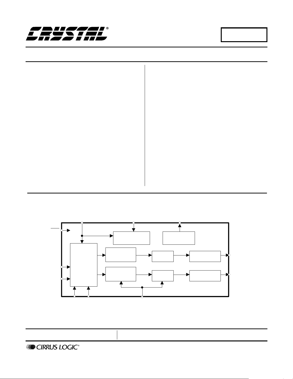
SCLK/DEM1
RST
Interpolation
Serial
LRCK
SDATA
Input
Interface
DIF0
Interpolation
DIF1
Preliminary Product Information
P.O. Box 17847, Austin, Texas 78760
(512) 445 7222 FAX: (512) 445 7581
http://www.cirrus.com
DEM0
De-emphasis
Filter
Filter
MCLK
This document contains information for a new product.
Cirrus Logic reserves the right to modify this product without notice.
∆Σ
∆Σ
Copyright Cirrus Logic, Inc. 2000
(All Rights Reserved)
MUTEC
External
Mute Control
DAC
DAC
Analog Filter
Analog Filter
AOUTL
AOUTR
NOV ‘00
DS297PP3
1

TABLE OF CONTENT
1. CHARACTERISTICS AND SPECIFICATIONS .................................. ....... ..... 5
ANALOG CHARACTERISTICS...................................................................5
ANALOG CHARACTERISTICS...................................................................6
ANALOG CHARACTERISTICS...................................................................7
POWER AND THERMAL CHARACTERISTICS ......................................... 8
DIGITAL CHARACTERISTICS.................................................................... 8
RECOMMENDED OPERATING CONDITIONS.......................................... 9
SWITCHING CHARACTERISTICS ........................................... ...... ....... ... 10
2. TYPICAL CONNECTION DIAGRAM ............................................................12
3. PIN DESCRIPTION .......................... ...... ....... ............................................. ... 13
4. APPLICATIONS ............................................................................................ 16
4.1 Grounding and Power Supply Decoupling ......................................... 16
4.2 Oversampling Modes ......................................................................... 16
4.3 Recommended Power-up Sequence .................................................16
4.4 Popguard
5. INTERPOLATION FILTER RESPONSE PLOTS .............................. 17
6. DIGITAL INTERFACE FORMATS ............................................. 19
7. ANALOG PERFORMANCE PLOTS ............. ...... ...... ....... ...... ....... ...... ....... ... 21
8. PARAMETER DEFINITIONS ........................................................................ 26
Total Harmonic Distortion + Noise (THD+N) .............................................26
Dynamic Range.........................................................................................26
Interchannel Isolation................................................................................. 26
Interchannel Gain Mismatch......................................................................26
Gain Error..................................................................................................26
Gain Drift.................................................................................................... 26
9. REFERENCES ..............................................................................................26
10. PACKAGE DIMENSIONS ........................................................................... 27
®
Transient Control ............................................................16
CS4340
Contacting Cirrus Logic Support
For a complete listing of Direct Sales, Distributor, and Sales Representative contacts, visit the Cirrus Logic web site at:
http://www.cirrus.com/corporate/contacts/
Preliminary product inf o rmation describes products whi c h are i n production, but for wh i ch f ull characterization data i s not yet available. Advance p rodu ct i nformation describes products which are in development and subject to development changes. Cirrus Logic, Inc. has made best efforts to ensure that the information
contained in this document i s accurat e and reli able. However , t he infor mation is subje ct to chang e without noti ce and is provi d ed “AS IS” without warrant y of
any kind (express or implied). No responsibility is assumed by Cirrus Logic, Inc. for the use of this information, nor for infringements of patents or other ri g ht s
of third parties. This document is the pro perty of Cirrus Logi c, Inc. and i mplie s no licen se under patents, copyrights, tr ademarks, or trade secre ts. No part of
this publication may be copied, reproduced , stored in a retrieval system, or transmitted, in any form or by any means (electronic, mechanical, photographic, or
otherwise) without the pr i or writ ten consent of Cirrus Logic, Inc. Items from any Cirrus Logic website or di sk may be printed for use by the user. However, no
part of the printout or electronic files may be copied, reproduced, stored in a retrieval system, or transmitted, in any form or by any means (electronic, mechanical,
photographic, or otherwise) without the prior written consent of Cirrus Logic, Inc.Furthermore, no part of this publication may be used as a basis for manufacture
or sale of any items without the prior written consent of Cirrus Logic, Inc. The names of products of Cirrus Logic, Inc. or other vendors and suppliers appearing
in this document may be trademarks or service marks of their respective owners which may be registered in some jurisdictions. A list of Cirrus Logic, Inc. trademarks and service marks can be found at http://www.cirrus.com.
2 DS297PP3

LIST OF FIGURES
Figure 1. External Serial Mode Input Timing ............................................................. 11
Figure 2. Internal Serial Mode Input Timing .............................................. ...... ....... ... 1 1
Figure 3. Internal Serial Clock Generation ................................................ ...... .......... 11
Figure 4. Typical Connection Diagram ............................ ...... ....... ...... ....... ...... ....... ... 12
Figure 5. Base-Rate Stopband Rejection.................................................................. 17
Figure 6. Base-Rate Transition Band ........................................................................ 17
Figure 7. Base-Rate Transition Band (Detail)............................................................ 17
Figure 8. Base-Rate Passband Ripple ...................................................................... 17
Figure 9. High-Rate Stopband Rejection................................................................... 17
Figure 10. High-Rate Transition Band....................................................................... 17
Figure 11. High-Rate Transition Band (Detail) .......................................................... 18
Figure 12. High-Rate Passband Ripple..................................................................... 18
Figure 13. Output Test Load...................................................................................... 18
Figure 14. Maximum Loading.................................................................................... 18
Figure 15. Power vs. Sample Rate (VA = 5V) ........................................................... 18
Figure 16. CS4340 Format 0 (I
Figure 17. CS4340 Format 1..................................................................................... 19
Figure 18. CS4340 Format 2..................................................................................... 20
Figure 19. CS4340 Format 3..................................................................................... 20
Figure 20. De-Emphasis Curve ................................................................................. 21
Figure 21. FFT 0 dB input, BRM, VA = 3V ................................................................ 22
Figure 22. FFT -60 dB input, BRM, VA = 3V............................................................. 22
Figure 23. FFT Idle Noise, BRM, VA = 3V................................................................. 22
Figure 24. Fade-to-Noise Linearity, BRM, VA = 3V................................................... 22
Figure 25. THDN vs Ampl, BRM, VA = 3V ................................................................ 22
Figure 26. THDN vs Freq, BRM, VA = 3V................................................................. 22
Figure 27. FFT 0 dB input, BRM, VA = 5V ................................................................ 23
Figure 28. FFT -60 dB input, BRM, VA = 5V............................................................. 23
Figure 29. FFT Idle Noise, BRM, VA = 5V................................................................. 23
Figure 30. Fade-to-Noise Linearity, BRM, VA = 5V................................................... 23
Figure 31. THDN vs Ampl, BRM, VA = 5V ................................................................ 23
Figure 32. THDN vs Freq, BRM, VA = 5V................................................................. 23
Figure 33. FFT 0 dB input, HRM, VA = 3V ................................................................ 24
Figure 34. FFT -60 dB input, HRM, VA = 3V............................................................. 24
Figure 35. FFT Idle Noise, HRM, VA = 3V ................................................................ 24
Figure 36. Fade-to-Noise Linearity, HRM, VA = 3V................................................... 24
Figure 37. THDN vs Ampl, HRM, VA = 3V................................................................ 24
Figure 38. THDN vs Freq, HRM, VA = 3V................................................................. 24
Figure 39. FFT 0 dB input, HRM, VA = 5V ................................................................ 25
Figure 40. FFT -60 dB input, HRM, VA = 5V............................................................. 25
Figure 41. FFT Idle Noise, HRM, VA = 5V ................................................................ 25
Figure 42. Fade-to-Noise Linearity, HRM, VA = 5V................................................... 25
Figure 43. THDN vs Ampl, HRM, VA = 5V................................................................ 25
Figure 44. THDN vs Freq, HRM, VA = 5V................................................................. 25
2
S)............................................................................. 19
CS4340
DS297PP3 3

LIST OF TABLES
Table 1. Internal Serial Clock Mode .......................................................................... 14
Table 2. External Serial Clock Mode ......................................................................... 14
Table 3. Common Master Clock Frequencies ........................................................... 14
Table 4. Digital Interface Format - DIF1 and DIF0 ................................................... 15
CS4340
4 DS297PP3
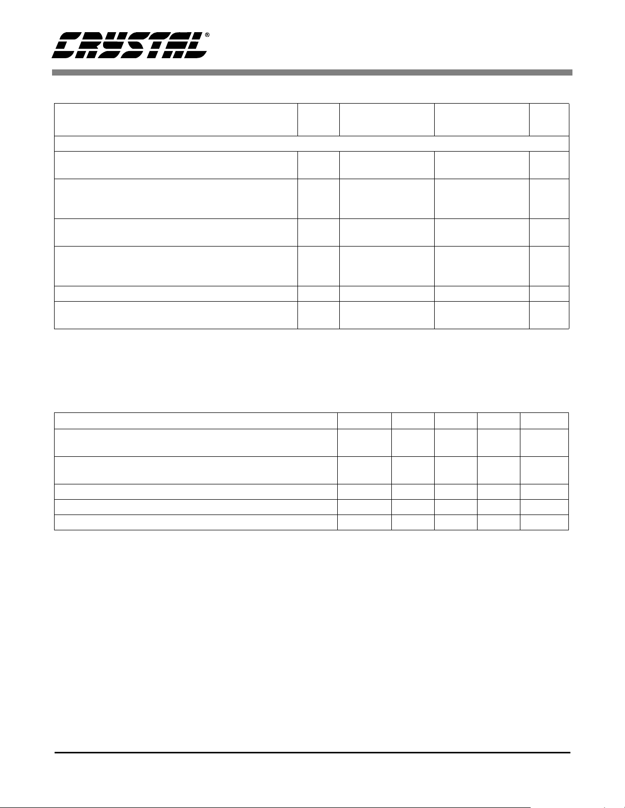
1. CHARACTERISTICS AND SPECIFICATIONS
CS4340
ANALOG CHARACTERISTICS (Test conditions (unless otherwise specified): T
VA = 5 V; Logic "0" = AGND;Full-Scale Output Sine Wave, 997 Hz; MCLK = 12.288 MHz; Fs for Base-rate Mode =
48 kHz, SCLK = 3.072 MHz, Measurement Bandwidth 10 Hz to 20 kHz, unless otherwise specified; Fs for HighRate Mode = 96 kHz, SCLK = 6.144 MHz, Measurement Bandwidth 10 Hz to 40 kHz, unless otherwise specified.
Test load R
= 10 kΩ, CL = 10 pF (see Figure 13)
L
Parameter
Base-rate Mode High-Rate Mode
Symbol Min Typ Max Min Typ Max Unit
= 25 °C; Logic "1" =
A
CS4340-KS Dynamic Performance for VA = 5 V (Note 1)
Specified Temperature Range T
Dynamic Range (Note 2)
18 to 24-Bit unweighted
A-Weighted
16-Bit unweighted
A-Weighted
Total Harmonic Distortion + Noise (Note 2)
18 to 24-Bit 0 dB
-20 dB
-60 dB
16-Bit 0 dB
-20 dB
-60 dB
Interchannel Isolation (1 kHz) - 102 - - 102 - dB
A
THD+N
-10 - 70 -10 - 70 °C
93
96
-
-
-
-
-
-
-
-
98
101
95
97
-91
-78
-38
-90
-75
-35
-
-
-
-
-86
-
-
-
-
-
91
95
96
100
-
-
-
-
-
-
-
-
94
97
-89
-76
-36
-89
-74
-34
-
-
-
-
-84
-
-
-
-
-
dB
dB
dB
dB
dB
dB
dB
dB
dB
dB
CS4340-KS Dynamic Performance for VA = 3 V (Note 1)
Specified Temperature Range T
Dynamic Range (Note 2)
18 to 24-Bit unweighted
A-Weighted
16-Bit unweighted
A-Weighted
Total Harmonic Distortion + Noise (Note 2)
18 to 24-Bit 0 dB
-20 dB
-60 dB
16-Bit 0 dB
-20 dB
-60 dB
Interchannel Isolation (1 kHz) - 102 - - 102 - dB
A
THD+N
-10 - 70 -10 - 70 °C
89
92
-
-
-
-
-
-
-
-
94
97
93
96
-94
-74
-34
-93
-73
-33
-
-
-
-
-88
-
-
-
-
-
87
91
92
96
-
-
-
-
-
-
-
-
92
96
-92
-72
-32
-91
-72
-32
-
-
-
-
-87
-
-
-
-
-
dB
dB
dB
dB
dB
dB
dB
dB
dB
dB
Notes: 1. CS4340-KS parts ar e test e d at 25 °C and Min/Max perform an ce nu mb e rs are gua ran t ee d ac r oss the
specified temp er at ure r an ge, T
2. One-half LSB of triangular PDF dither is added to data.
DS297PP3 5
.
A
CS4340
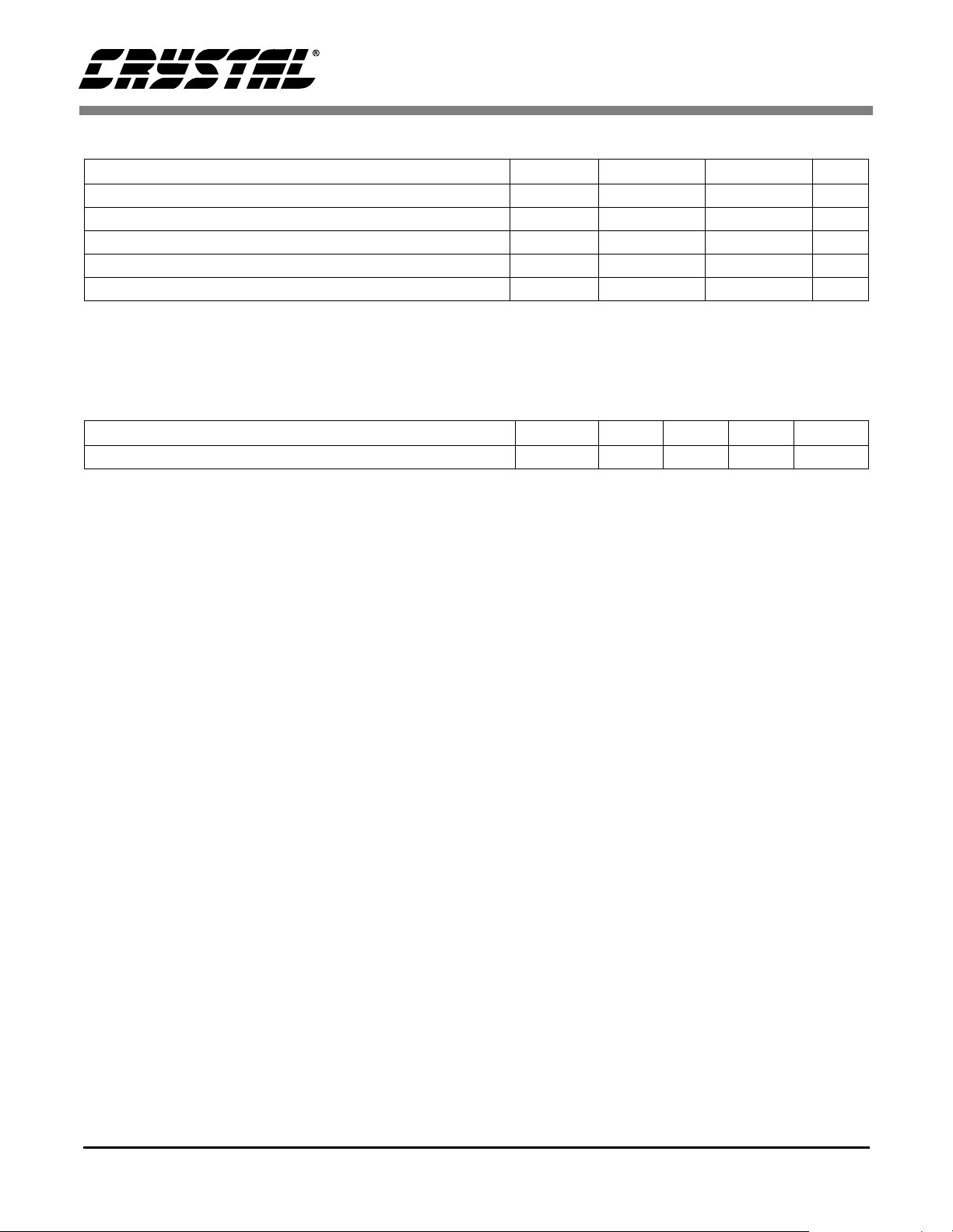
ANALOG CHARACTERISTICS (Continued)
Base-rate Mode High-Rate Mode
Parameter
CS4340-BS Dynamic Performance for VA = 5 V (Note 3)
Specified Temperature Range T
Dynamic Range (Note 2)
18 to 24-Bit unweighted
A-Weighted
16-Bit unweighted
A-Weighted
Total Harmonic Distortion + Noise (Note 2)
18 to 24-Bit 0 dB
-20 dB
-60 dB
16-Bit 0 dB
-20 dB
-60 dB
Interchannel Isolation (1 kHz) - 102 - - 102 - dB
CS4340-BS Dynamic Performance for VA = 3 V (Note 3)
Specified Temperature Range T
Dynamic Range (Note 2)
18 to 24-Bit unweighted
A-Weighted
16-Bit unweighted
A-Weighted
Total Harmonic Distortion + Noise (Note 2)
18 to 24-Bit 0 dB
-20 dB
-60 dB
16-Bit 0 dB
-20 dB
-60 dB
Interchannel Isolation (1 kHz) - 102 - - 102 - dB
Symbol Min Typ Max Min Typ Max Unit
A
THD+N
A
THD+N
-40 - 85 -40 - 85 °C
TBD
TBD
-
-
-
-
-
-
-
-
-40 - 85 -40 - 85 °C
TBD
TBD
-
-
-
-
-
-
-
-
98
101
95
97
-91
-78
-38
-90
-75
-35
94
97
93
96
-94
-74
-34
-93
-73
-33
-
-
-
-
TBD
-
-
-
-
-
-
-
-
-
TBD
-
-
-
-
-
TBD
TBD
-
-
-
-
-
-
-
-
TBD
TBD
-
-
-
-
-
-
-
-
96
100
94
97
-89
-76
-36
-89
-74
-34
92
96
92
96
-92
-72
-32
-91
-72
-32
-
-
-
-
TBD
-
-
-
-
-
-
-
-
-
TBD
-
-
-
-
-
dB
dB
dB
dB
dB
dB
dB
dB
dB
dB
dB
dB
dB
dB
dB
dB
dB
dB
dB
dB
Notes: 3. CS4340-BS parts are tested at the extremes of the specified temperature range and Min/Max
performance numbers are guaranteed across the specified temperature range, T
taken at 25 °C.
6 DS297PP3
. Typical numb ers are
A
CS4340
ANALOG CHARACTERISTICS (Continued)
Parameters Symbol Min Typ Max Units
Analog Output
Full Scale Output Voltage 0.63•VA 0.7•VA 0.77•VA Vpp
Quiescent Voltage V
Interchannel Gain Mismatch - 0.1 - dB
Gain Drift - 100 - ppm/°C
AC-Load Resistance (Note 4) R
Load Capacitance (Note 4) C
Parameter
Symbol Min Typ Max Min Typ Max Unit
Q
L
L
Base-rate Mode High-Rate Mode
Combined Digital and On-chip Analog Filter Response (Note 5)
Passband (Note 6)
to -0.05 dB corner
to -0.1 dB corner
to -3 dB corner
Frequency Response 10 Hz to 20 kHz -.02 - +.08 -0.06 - 0.2 dB
StopBand .5465 - - .577 - - Fs
StopBand Attenuation (Note 7) 50 - - 55 - - dB
Group Delay tgd - 9/Fs - - 4/Fs - s
Passband Group Delay Deviation 0 - 40 kHz
0 - 20 kHz
De-emphasis Error Fs = 32 kHz
(Relative to 1 kHz) Fs = 44.1 kHz
Fs = 48 kHz
0
-
0
-
--±0.36/Fs
-
-
-
-
-
-
-
-
-
-0.5•VA- VDC
3--kΩ
--100pF
.4535
-
.4998
-
-
+.2/-.1
+.05/-.14
+0/-.22
0
0
--±1.39/Fs
-
-
-
±0.23/Fs--
(Note 8)
.4621
.4982
Fs
Fs
Fs
s
s
dB
dB
dB
Notes: 4. Refer to Figure 14.
5. Filter response is gu ara nt e ed by de sig n.
6. Response is clock dependent and will scale with Fs. Note that the response plots (Figures 5-12) have
been normalized to Fs and can be de-normalized by multiplying the X-axis scale by Fs.
7. For Base-Rate Mode, the measurement bandwidth is 0.5465 Fs to 3 Fs.
For High-Rate Mode, the measurement bandwidth is 0.577 Fs to 1.4 Fs.
8. De-emphasi s is not availab le in High - Rate Mode.
DS297PP3 7
POWER AND THERMAL CHARACTERISTICS
CS4340-KS CS4340-BS
Parameters Symbol Min Typ Max Min Typ Max Units
Power Supplies
Power Supply Current normal operation
VA = 5 V power-down state
Power Dissipation (No te 9)
VA = 5 V normal operation
power-down
Power Supply Current normal operation
VA = 3 V power-down state
Power Dissipation (No te 9)
VA = 3 V normal operation
power-down
Package Thermal Resistance θ
Power Supply Rejection Ratio (1 kHz) (Note 10)
(60 Hz)
Notes: 9. Refer to Figure 15.
10. Valid with the recommended capacitor values on FILT+ and VQ as shown in Figure 4. Increasing the
capacitance will also increase the PSRR.
I
A
I
A
I
A
I
A
JA
PSRR -
-
-
-
-
-
-
-
-300.0942-
- 110 - - 110 - °C/Watt
-
156018
75
90
0.3
103014
60
40
CS4340
-
1560TBD-mA
-
-
-
-
-
-
-
75
-
0.3
-
1030TBD-mA
-
-
-300.09
-
60
-
40
µA
TBD-mW
mW
µA
TBD-mW
mW
-
-
dB
dB
DIGITAL CHARACTERISTICS (for -KS parts T
= -10 to 70°C; for -BS parts TA = -40 to 85°C;
A
VA = 2.7 V - 5.5 V)
Parameters Symbol Min Typ Max Units
High-Level Input Voltage VA = 5 V
VA = 3 V
Low-Level Input Voltage VA = 5 V
VA = 3 V
Input Leakage Current I
V
IH
V
IL
in
2.0
2.0
-
-
-
-
-
-
-
-
0.8
0.8
--±10µA
Input Capacitance - 8 - pF
Maximum MUTEC Drive Current - 3 - mA
V
V
V
V
8 DS297PP3
CS4340
ABSOLUTE MAXIMUM RATINGS (AGND = 0 V; all voltages with respect to ground.)
Parameters Symbol Min Max Units
DC Power Supply VA -0.3 6.0 V
Input Current, Any Pin Except Supplies I
Digital Input Voltage V
Ambient Operating Temperature (power applied) T
Storage Temperature T
WARNING: Operation at or beyond these limits may result in permanent damage to the device. Normal operation is
not guaranteed at these extremes.
in
IND
A
stg
RECOMMENDED OPERATING CONDITIONS (AGND = 0V; all voltages with respe ct to
ground.)
Parameters Symbol Min Typ Max Units
DC Power Supply VA 2.7 5.0 5.5 V
- ±10 mA
-0.3 VA+0.4 V
-55 125 °C
-65 150 °C
DS297PP3 9

CS4340
SWITCHING CHARACTERISTICS (VA = 2.7 V - 5.5 V; Inputs: Logic 0 = 0 V, Logic 1 = VA, CL =
20 pF; for -KS parts T
Input Sample Rate Base-Rate Mode
MCLK Pulse Width High MCLK/LRCK = 512 10 - 1000 ns
MCLK Pulse Width Low MCLK/LRCK = 512 10 - 1000 ns
MCLK Pulse Width High MCLK / LRCK = 384 or 192 21 - 1000 ns
MCLK Pulse Width Low MCLK / LRCK = 384 or 192 21 - 1000 ns
MCLK Pulse Width High MCLK / LRCK = 256 or 128 31 - 1000 ns
MCLK Pulse Width Low MCLK / LRCK = 256 or 128 31 - 1000 ns
External SCLK Mode
LRCK Duty Cycle (External SCLK only) 40 50 60 %
SCLK Pulse Width Low t
SCLK Pulse Width High t
SCLK Period MCLK / LRCK = 512, 256 or 384 t
SCLK Period MCLK / LRCK = 128 or 192 t
SCLK rising to LRCK edge delay t
SCLK rising to LRCK edge setup time t
SDATA valid to SCLK rising setup time t
SCLK rising to SDATA hold time t
Internal SCLK Mode
LRCK Duty Cycle (Internal SCLK only) (Note 11) - 50 - %
SCLK Period (Note 12) t
SCLK rising to LRCK edge t
= -10 to 70°C; for -BS parts TA = -40 to 85°C)
A
Parameters Symbol Min Typ Max Units
High-Rate Mode
Fs 2
sclkl
sclkh
sclkw
sclkw
slrd
slrs
sdlrs
sdh
sclkw
sclkr
---------------------128()Fs
------------------
---------------SCLK
50
20 - - ns
20 - - ns
1
1
64()Fs
20 - - ns
20 - - ns
20 - - ns
20 - - ns
1
--µs
-
-
50
100
kHz
kHz
--ns
--ns
--ns
tsclkw
----------------- 2
SDATA valid to SCLK rising setup time t
SCLK rising to SDATA hold time
MCLK / LRCK = 512, 256 or 128
SCLK rising to SDATA hold time
MCLK / LRCK = 384 or 192
sdlrs
t
sdh
t
sdh
1
----------------------10+
512()Fs
1
----------------------15+
512()Fs
1
----------------------15+
384()Fs
--ns
--ns
--ns
Notes: 11. In Internal SCLK Mode, the Duty Cycle must be 50% +/− 1/ 2 MCLK Peri od.
12. The SCLK / LRCK ratio may be either 32, 48, or 64. This ratio depends on part type and MCLK/LRCK
ratio. (See figures 16-19)
10 DS297PP3

LRCK
SCLK
t
slrd
t
slrs
t
sclkl
t
sclkh
CS4340
t
sdh
SDATA
t
sdlrs
Figure 1. External Serial Mode Input Timing
LRCK
t
sclkr
SDATA
t
sdlrstsdh
*INTERNAL SCLK
Figure 2. Internal Serial Mode Input Timing
*The SCLK pulses shown are internal to the CS4340.
t
sclkw
LRCK
MCLK
*INTERNAL SCLK
SDATA
1
N
2
N
Figure 3. Internal Serial Clock Generation
* The SCLK pulses shown are internal to the CS4340.
N equals MCLK divided by SCLK
DS297PP3 11

2. TYPICAL CONNECTION DIAGRAM
0.1 µF
AOUTL
MUTEC
FILT+
VQ
REF_GND
AOUTR
3.3 µF
15
+
Ω
10 k
16
9
10
.1 µF
11
3.3 µF
12
+
Ω
10 k
Audio
Data
Processor
External Clock
Mode
Configuration
2
3
4
5
6
7
8
1
14
VA
SDATA
SCLK/DEM1
LRCK
CS4340
MCLK
DIF1
DIF0
DEM0
RST
AGND
13
+
+
1µF
1µF
560
560
+5Vto+3V
Ω
C
+
1µF
0.1 µF
Ω
C
C=
OPTIONAL
MUTE
CIRCUIT
+ 560
R
L
π
FSRL 560
4
R
R
Left
Audio
Output
L
Right
Audio
Output
L
CS4340
Figure 4. Typical Connection Diagram
12 DS297PP3

3. PIN DESCRIPTION
CS4340
Reset RST MUTEC Mute Control
Serial Data SDATA AOUTL Left Analog Output
Serial Clock / De-emphasis SCLK/DEM1 VA Analog Power
Left/Right Clock LRCK AGND Analog Ground
Master Clock MCLK AOUTR Right Analog Output
Digital Interface Format DIF1 REF_GND Reference Ground
Digital Interface Format DIF0 VQ Quiescent Voltage
De-emphasis DEM0 FILT+ Positive Voltage Reference
RST 1 Reset (
SDATA 2 Serial Audio Data (
SCLK 3 Serial Clock (
Input
) - The device enters a low power mode and all intern al state machi nes are reset to
the default settings when low. RST
master and left/right clocks are stable.
Input
) - Two’s complement MSB-first serial data is input on this pin. The
data is clocked into SDATA via the serial clock and the channel is determined by the Left/Right
clock. The required relationship between the Left/Right clock, serial clock and serial data is
defined by the DIF1-0 pins. The options are detailed in Figures 16-19.
Input
) - Clocks the individual bits of the serial data into the SDATA pin. The
required relationship bet w een the L eft/ Righ t cl oc k, s eri al c loc k and serial data is defined by the
DIF1-0 pins. The options are detailed in Figures 16-19.
The CS4340 supports both internal and external serial clock generation modes. Internal SCLK
mode is used to gain acc ess to extra de-emphasis modes.
Internal Serial Clock Mode
derived and synchronous with th e mast er cloc k and lef t/right c lock. The SCLK/ LRCK freq uency
ratio is either 32, 48, or 64 depending upon the DIF1-0 pins as shown in Figures 16-19. Operation in th is mode is identical to op eration with an external serial clock synchronized with LRCK.
External Serial Clock Mode
16 low to high transitions are detected on the SCLK pin during any phase of the LRCK period.
The device will revert to Inter nal S eria l Clo ck Mod e if no lo w to hi gh tra ns itions are d ete cted on
the SCLK pin for 2 consecutive periods of LRCK.
- In the Internal Serial Clock Mode, the serial clock is internally
- The CS4340 will enter the External Serial Clock Mode whenever
161
152
143
134
125
116
107
98
should be held low during pow er-up until the power supp ly,
DS297PP3 13

CS4340
DEM1 and DEM0 3 & 8 De-emphasis Control (
filter response, Figure 20, requ ires reconfi guration of th e digital filt er to maintain the pro per filter
response for 32, 44.1 or 48 kHz sample rates. When using Internal Serial Clock Mode, as
described above, Pin 3 is available for de-emphasis control, DEM1, and all de-emphasis filters
are available, Table 3. When using External Serial Clock Mode, as described above, Pin 3 is
not available for de-emphasis use and only the 44.1 kHz de-emphasis filter is available,
Table 4. NOTE: De-emphasis is not available in High-Rate Mode.
LRCK 4 Left/Right Clock (
input on the serial audio data input, SDATA. The frequency of the Left/Right clock must be at
the input sample rate. Audio samples in Left/Right sample pairs will be simultaneously output
from the digital-to-analog converter whereas Right/Left pairs will exhibit a one sample period
difference. The req uired relat ionsh ip between th e Left/Right c lock, seria l clock a nd serial d ata is
defined by the DIF1-0 pins. The options are detailed in Figures 16-19.
MCLK 5 Master Clock (
sample rate in Base Rate Mode (BRM) and either 128x or 192x the input sample rate in High
Rate Mode (HRM). Table 3 illustrates several standard audio sample rates and the required
master clock frequenc ie s.
Input
Input
) - The master clock fre quenc y mus t be ei ther 256 x, 384x o r 512x the inp ut
Input
) - Implementation of the sta nda rd 15µs/50µs digital de-emphasis
DEM1 DEMO DESCRIPTION
00Disabled
0144.1kHz
1048kHz
1132kHz
Table 1. Internal S erial Clock Mode
DEMO DESCRIPTION
0 Disabled
1 44.1kH z
Table 2. External Serial Clock Mode
) - The Left/Right clock determines which channel is currently being
MCLK (MHz)
Sample
HRM BRM
Rate
(kHz)
128x 192x 256x 384x 512x
32 4.0960 6.1440 8.1920 12.2880 16.3840
44.1 5.6448 8.4672 11.2896 16.9344 22.5792
48 6.1440 9.2160 12.2880 18.4320 24.5760
64 8.1920 12.2880 - - -
88.2 11.2896 16.9344 - - 96 12.2880 18.4320 - - -
Table 3. Common Master Clock Frequencies
14 DS297PP3

CS4340
DIF1 and DIF0 6 & 7 Digital Interface Format (I
clock and serial data is defined by the Digital Interface Format and the options are detailed in
Figures 16-19
.
DIF1 DIF0 DESCRIPTION FORMAT FIGURE
00I
0 1 Left Justified, up to 24-bit data 1 17
1 0 Right Justified, 24-bit Data 2 18
1 1 Right Justified, 16-bit Data 3 19
nput
2
S, up to 24-bit data 0 16
Table 4. Digital Interface Format - DIF1 and DIF0
FILT+ 9 Positive Voltage Reference (
external capacitor is required from FILT+ to analog ground, as shown in Figure 4. The recommended value will typically provide 60 dB of PSRR at 1 kHz and 40 dB of PSRR at 60 Hz.
FILT+ is not intended to supply external current. FILT+ has a typical source impedance of
250 kΩ and any current drawn from this pin will alter device performance.
VQ 10 Quiescent Voltage (
cally 50% of VA. Capacitors must be connected from VQ to analog ground, as shown in
Figure 4. VQ is not intended to supply external current. VQ has a typical source impedence of
250 kΩ and any current drawn from this pin will alter device performance.
REF_GND 11 Reference Ground (
nected to analog ground.
AOUTR and AOUTL 12 & 15Analog Outputs (
teristics specifications table.
AGND 13 Ground (
VA 14 Analog Power (
MUTEC 16 Mute Control (
muting, master clock to left/right clock frequency ratio is incorrect or power-down. This pin is
intended to be used as a control for an external mute circuit to prevent the clicks and pops that
can occur in any singl e supply system. Use of Mute Control i s not mandato ry but re commended
for designs requiring the absolute minimum in extraneous clicks and pops.
Input
Output
) - Filter connection for internal quiescent reference voltage, typi-
Input
) - Ground reference for the internal sampling circuits. Must be con-
Output
) - The full scale analog o utp ut le ve l is specified in the Analog C hara c-
) - Ground Reference.
Input
) - Analog power supply. Typically 3 to 5 VDC.
Output
) - The Mute Control pin goes high during power-up initialization, reset,
) - The required relationship be tween the Lef t/Right cloc k, serial
Output
) - Positive reference for internal sampling circuits. An
DS297PP3 15

CS4340
4. APPLICATIONS
4.1 Grounding and Power Supply Decoupling
As with any high resolution converter, the CS4340
requires careful attention to power supply and
grounding arrangements to optimize performance.
Figure 4 shows the recommended power arrangement with VA connected to a clean supply. Decoupling capacitors should be located as close to the
device package as possible.
4.2 Oversampling Modes
The CS4340 operates in one of two oversampling
modes. Base Rate Mode supports input sample
rates up to 50 kHz while High Rate Mode supports
input sample rates up to 100 kHz. The devices operate in Base Rate Mode (BRM) when
MCLK/LRCK is 256, 384 or 512 and in High Rate
Mode (HRM) when MCLK/LRCK is 128 or 192.
4.3 Recommended Power-up Sequence
RST should be held low until the power supply,
master and left/right clocks are stable.
4.4 Popguard® Transient Control
The CS4340 uses Popguard® technology to minimize the effects of output transients during powerup and power-down. This technique, when used
with external DC-blocking capacitors in se ries with
the audio outputs, minimizes the audio transients
commonly produced by single-ended single-supply
converters.
To prevent transients at power-down, the device
must first enter its power-down state by setting the
RST pin low. When this occurs, audio output ceases and the internal output buffers are disconnected
from AOUTL and AOUTR. In their place, a softstart current sink is substituted which allows the
DC-blocking capacitors to slowly discharge. Once
this charge is dissipated, the power to the device
may be turned off and the system is ready for the
next power-on.
To prevent an audio transient at the next power-on,
it is necessary to ensure that the DC-blocking capacitors have fully discharged before turning off
the power or exiting the power-down state. If not, a
transient will occur when the audio outputs are initially clamped to AGND. The time that the device
must remain in the power-down state is related to
the value of the DC-blocking capacitance. For ex-
ample, with a 3.3 µF capacitor, the minimum power-down time will be approximately 0.4 seconds.
Use of the Mute Control function is recommended
for designs requiring the absolute minimum in extraneous clicks and pops. Also, use of the Mute
Control function can enable the system designer to
achieve idle channel noise/signal-to-noise ratios
which are only limited by the external mute circuit.
See the CDB4340/41 data sheet for a suggested
mute circuit.
When the device is initially powered-up, the audio
outputs, AOUTL and AOUTR, are clamped to
AGND. Following a delay of approximately 1000
sample periods, each output begins to ramp toward
the quiescent voltage. Approximately 10,000
left/right clock cycles later, the outputs reach V
and audio output begins. This gradual voltage
ramping allows time for the external DC-blocking
capacitor to charge to the quiescent voltage, minimizing the power-up transient.
16 DS297PP3
Q

5. INTERPOLATION FILTER RESPONSE PLOTS
Figure 5. Base-Rate Stopband Rejection Figure 6. Base-Rate Transition Band
CS4340
Figure 7. Base-Rate Transition Band (Detail) Figure 8. Base-Rate Passband Ripple
Figure 9. High-Rate Stopband Rejection Figure 10. High-Rate Transition Band
DS297PP3 17

CS4340
100
50
75
25
2.5
51015
Safe Operating
Region
Capacitive Load -- C (pF)
L
Resistive Load -- R (kΩ)
L
125
3
20
Figure 14. Maximum Loading
Figure 11. H i gh-Rate Transition Band (Detail) Figure 12. High-Rate P assband Ripple
3.3 µF
AOUTx
+
V
out
AGND
R
L
Figure 13. Output Test Load
75
70
65
60
Power (mW)
55
50
30
C
L
M
R
B
M
R
H
40 50 60 70 80 90
Sample Rate (kHz)
100
18 DS297PP3
Figure 15. Power vs. Sample Rate (VA = 5V)

6. DIGITAL INTERFACE FORMATS
CS4340
LRCK
SCLK
SDATA +3 +2 +1
MSB
-1 -2 -3 -4 -5
Left Channel
+5 +4
Internal SCLK Mode Extern al SCLK Mode
2
I
S, 16-Bit data and INT SCLK = 32 Fs i f
MCLK/LRCK = 512, 256 or 128
2
S, up to 24-Bit data and INT SCLK = 48 Fs if
I
MCLK/LRCK = 384 or 192
Figure 16. CS4340 Format 0 (I
LSB
Right Channel
+3 +2 +1
MSB
-1 -2 -3 -4
2
I
S, up to 24-Bit Data
+5 +4
LSB
Data Valid on Rising Edge of SCLK
2
S)
LRCK
SCLK
SDATA +3 +2 +1
MSB
-1 -2 -3 -4 -5
Left Channel
+5 +4
LSB
MSB
-1 -2 -3 -4
Right Channel
+3 +2 +1
+5 +4
LSB
Internal SCLK Mode Extern al SCLK Mode
Left Justified, up to 24-Bit Data
INT SCLK = 64 Fs if MCLK/LRCK = 512, 256 or 128
Left Justified, up to 24-Bit Data
Data Valid on Rising Edge of SCLK
INT SCLK = 48 Fs if MCLK/LRCK = 384 or 192
Figure 17. CS4340 Format 1
DS297PP3 19

CS4340
LRCK
SCLK
SDATA
0
Left Channel
23 22 21 20 19 18
32 clocks
65432107
Internal SCLK Mode Extern al SCLK Mode
Right Justified, 24-Bit Data
INT SCLK = 64 Fs if MCLK/LRCK = 512, 256 or 128
INT SCLK = 48 Fs if MCLK/LRCK = 384 or 192
Figure 18. CS4340 Format 2
Right Channel
23 22 21 20 19 18
65432107
Right Justified, 24-Bit Data
Data Valid on Rising Edge of SCLK
SCLK Must Have at Least 48 Cycles per LRCK Period
LRCK
SCLK
SDATA
Left Channel
15 14 13 12 11 10
32 clocks
6543210987
15 14 13 12 11 10
Right Channel
6543210987
Internal SCLK Mode External SCLK Mode
Right Justified, 16-Bit Data
INT SCLK = 32 Fs if MCLK/LRCK = 512, 256 or 128
INT SCLK = 48 Fs if MCLK/LRCK = 384 or 192
Right Justified, 16-Bit Data
Data Valid on Rising Edge of SCLK
SCLK Must Have at Least 32 Cycles per LRCK Period
Figure 19. CS4340 Format 3
20 DS297PP3

Gain
dB
0dB
-10dB
CS4340
T1=50 µs
T2 = 15 µs
F1 F2
3.183 kHz 10.61 kHz
Figure 20. De-Emphasis Curve
7. ANALOG PERFORMANCE PLOTS
The following CS4340 Analog Performance Plots
were taken from the CDB4340 evaluation board
using the Audio Precision Dual Domain System
Two Cascade. All Base Rate Mode (BRM) plots
were taken at a 48 kHz sample rate with a 20 Hz to
20 kHz bandwidth using a 20 kHz low-pass brick-
Frequency
wall filter in the DSP Analyzer. All High Rate
Mode (HRM) plots were taken at a 96 kHz sample
rate with a 20 Hz to 40 kHz bandwith using a
40 kHz brickwall filter in the DSP Analyzer.
DS297PP3 21

CS4340
-140
+0
-130
-120
-110
-100
-90
-80
-70
-60
-50
-40
-30
-20
-10
d
B
r
A
2k 20k4k 6k 8k 10k 12k 14k 16k 18k
Hz
-140
+0
-130
-120
-110
-100
-90
-80
-70
-60
-50
-40
-30
-20
-10
d
B
r
A
2k 20k4k 6k 8k 10k 12k 14k 16k 18k
Hz
-105
-85
-104
-103
-102
-101
-100
-99
-98
-97
-96
-95
-94
-93
-92
-91
-90
-89
-88
-87
-86
d
B
r
A
-60 +0-55 -50 -45 -40 -35 -30 -25 -20 -15 -10 -5
dBFS
+0
-10
-20
-30
-40
-50
-60
d
B
-70
r
A
-80
-90
-100
-110
-120
-130
-140
2k 20k4k 6k 8k 10k 12k 14k 16k 18k
Figure 21. FFT 0 dB input, BRM, VA = 3V Figure 22. FFT -60 dB input, BRM, VA = 3V
+20
+18
+16
+14
+12
+10
+8
d
+6
B
r
+4
A
+2
+0
-2
-4
-6
-8
-10
-100 +0-90 -80 -70 -60 -50 -40 -30 -20 -10
Figure 23. FFT Idle Noise, BRM, VA = 3V Figure 24. Fade-to-Noise Linearity, BRM, VA = 3V
Hz
dBFS
22 DS297PP3
Figure 25. THDN vs Ampl, BRM, VA = 3V Figure 26. THDN vs Freq, BRM, VA = 3V
-85
-86
-87
-88
-89
-90
-91
-92
-93
d
-94
B
-95
r
-96
A
-97
-98
-99
-100
-101
-102
-103
-104
-105
20 20k50 100 200 500 1k 2k 5k 10k
Hz

CS4340
-140
+0
-130
-120
-110
-100
-90
-80
-70
-60
-50
-40
-30
-20
-10
d
B
r
A
2k 20k4k 6k 8k 10k 12k 14k 16k 18k
Hz
-140
+0
-130
-120
-110
-100
-90
-80
-70
-60
-50
-40
-30
-20
-10
d
B
r
A
2k 20k4k 6k 8k 10k 12k 14k 16k 18k
Hz
-105
-85
-104
-103
-102
-101
-100
-99
-98
-97
-96
-95
-94
-93
-92
-91
-90
-89
-88
-87
-86
d
B
r
A
-60 +0-55 -50 -45 -40 -35 -3 0 -25 -20 -15 -10 -5
dBFS
+0
-10
-20
-30
-40
-50
-60
d
B
-70
r
A
-80
-90
-100
-110
-120
-130
-140
2k 20k4k 6k 8k 10k 12k 14k 16k 18k
Figure 27. FFT 0 dB input, BRM, VA = 5V Figure 28. FFT -60 dB input, BRM, VA = 5V
+20
+18
+16
+14
+12
+10
+8
d
+6
B
r
+4
A
+2
+0
-2
-4
-6
-8
-10
-100 +0-90 -80 -70 -60 -50 -40 -30 -20 -10
Hz
dBFS
Figure 29. FFT Idle Noise, BRM, VA = 5V Figure 30. Fade-to-Noise Linearity, BRM, VA = 5V
DS297PP3 23
Figure 31. THDN vs Ampl, BRM, VA = 5V Figure 32. THDN vs Freq, BRM, VA = 5V
-85
-86
-87
-88
-89
-90
-91
-92
-93
d
-94
B
-95
r
-96
A
-97
-98
-99
-100
-101
-102
-103
-104
-105
20 20k50 100 200 500 1k 2k 5k 10k
Hz

CS4340
-140
+0
-130
-120
-110
-100
-90
-80
-70
-60
-50
-40
-30
-20
-10
d
B
r
A
5k 40k10k 15k 20k 25k 30k 35k
Hz
-140
+0
-130
-120
-110
-100
-90
-80
-70
-60
-50
-40
-30
-20
-10
d
B
r
A
5k 40k10k 15k 20k 25k 30k 35k
Hz
-105
-85
-104
-103
-102
-101
-100
-99
-98
-97
-96
-95
-94
-93
-92
-91
-90
-89
-88
-87
-86
d
B
r
A
-60 +0-55 -50 -45 -40 -35 -30 -25 -20 -15 -10 -5
dBFS
+0
-10
-20
-30
-40
-50
-60
d
B
-70
r
A
-80
-90
-100
-110
-120
-130
-140
Figure 33. FFT 0 dB input, HRM, VA = 3V Figure 34. FFT -60 dB input, HRM, VA = 3V
d
B
r
A
Figure 35. FFT Idle Noise, HRM, VA = 3V Figure 36. Fade-to-Noise Linearity, HRM, VA = 3V
5k 40k10k 15k 20k 25k 30k 35k
+20
+18
+16
+14
+12
+10
+8
+6
+4
+2
+0
-2
-4
-6
-8
-10
-100 +0-90 -80 -70 -60 -50 -40 -30 -20 -10
Hz
dBFS
24 DS297PP3
Figure 37. THDN vs Ampl, HRM, VA = 3V Figure 38. THDN vs Freq, HRM, VA = 3V
-85
-86
-87
-88
-89
-90
-91
-92
-93
d
-94
B
-95
r
-96
A
-97
-98
-99
-100
-101
-102
-103
-104
-105
20 40k50 100 200 500 1k 2k 5k 10k 20k
Hz

CS4340
-140
+0
-130
-120
-110
-100
-90
-80
-70
-60
-50
-40
-30
-20
-10
d
B
r
A
5k 40k10k 15k 20k 25k 30k 35k
Hz
-140
+0
-130
-120
-110
-100
-90
-80
-70
-60
-50
-40
-30
-20
-10
d
B
r
A
5k 40k10k 15k 20k 25k 30k 35k
Hz
-105
-85
-104
-103
-102
-101
-100
-99
-98
-97
-96
-95
-94
-93
-92
-91
-90
-89
-88
-87
-86
d
B
r
A
-60 +0-55 -50 -45 -40 -35 -30 -25 -20 -15 -10 -5
dBFS
+0
-10
-20
-30
-40
-50
-60
d
B
-70
r
A
-80
-90
-100
-110
-120
-130
-140
Figure 39. FFT 0 dB input, HRM, VA = 5V Figure 40. FFT -60 dB input, HRM, VA = 5V
+20
+18
+16
+14
+12
+10
+8
d
+6
B
r
+4
A
+2
+0
-10
Figure 41. FFT Idle Noise, HRM, VA = 5V Figure 42. Fade-to-Noise Linearity, HRM, VA = 5V
5k 40k10k 15k 20k 25k 30k 35k
-2
-4
-6
-8
-100 +0-90 -80 -70 -60 -50 -40 -30 -20 -10
Hz
dBFS
DS297PP3 25
Figure 43. THDN vs Ampl, HRM, VA = 5V Figure 44. THDN vs Freq, HRM, VA = 5V
-85
-86
-87
-88
-89
-90
-91
-92
-93
d
-94
B
-95
r
-96
A
-97
-98
-99
-100
-101
-102
-103
-104
-105
20 40k50 100 200 500 1k 2k 5k 10k 20k
Hz

8. PARAMETER DEFINITIONS
Total Harmonic Distortion + Noise (THD+N)
A measure of crosstalk between the left and right channels. Measured for each channel at the converter’s
output with all zeros to the input under test and a full-scale signal applied to the other channel. Units in
decibels.
Dynamic Range
The ratio of the full scale rms value of the signal to the rms sum of all other spectral components over the
specified bandwidth. Dynamic range is a signal-to-noise measurement over the specified bandwidth
made with a -60 dBFS signal. 60 dB is then added to the resulting measurement to refer the measurement
to full scale. This technique ensures that the distortion components are below the noise level and do not
effect the measurement. This measurement technique has been accepted by the Audio Engineering Society, AES17-1991, and the Electronic Industries Association of Japan, EIAJ CP-307.
Interchannel Isolation
A measure of crosstalk between the left and right channels. Measured for each channel at the converter’s
output with all zeros to the input under test and a full-scale signal applied to the other channel. Units in
decibels.
Interchannel Gain Mismatch
The gain difference between left and right channels. Units in decibels.
CS4340
Gain Error
The deviation from the nominal full scale analog output for a full scale digital input.
Gain Drift
The change in gain value with temperature. Units in ppm/°C.
9. REFERENCES
1) "How to Achieve Optimum Performance from Delta-Sigma A/D & D/A Converters" by Steven Harris.
Paper presented at the 93rd Convention of the Audio Engineering Society, October 1992.
2) CDB4340 Evaluation Board Datasheet
26 DS297PP3

10.PACKAGE DIMENSIONS
16L SOIC (150 MIL BODY) PACKAGE DRAWING
1
b
CS4340
E
H
c
∝
L
SEATING
PLANE
D
A
e
A1
INCHES MILLIMETERS
DIM MIN NOM MAX MIN NOM MAX
A 0.053 0.064 0.069 1.35 1.63 1.75
A1 0.004 0.006 0.010 0.10 0.15 0.25
b 0.013 0.016 0.020 0.33 0.41 0.51
C 0.0075 0.008 0.010 0.19 0.20 0.25
D 0.386 0.390 0.394 9.80 9.91 10.00
E 0.150 0.154 0.157 3.80 3.90 4.00
e 0.040 0.050 0.060 1.02 1.27 1.52
H 0.228 0.236 0.244 5.80 6.0 6.20
L 0.016 0.025 0.050 0.40 0.64 1.27
∝ 0° 4° 8° 0° 4° 8°
JEDEC #: MS-012
Controling Dimension is Millimeters
DS297PP3 27

 Loading...