

CS4297
Product Data Sheet
FEATURES
n AC’97 1.03 Co mpatible
n Industry Leading Mixed Signal Technology
n 18-bit stereo full-duplex Codec with fixed 48 kHz
sampling rate
n Four analog line-level stereo inputs for connec-
tion from LINE IN, CD, VIDEO and AUX
n T wo analog line-level mono inputs for speaker-
phone and internal PC Beeper
n Mono microphone input switchable from two
external sourc e s
n High quality differential CD input
n Dual Stereo line level outputs
n Extensive power management support
®
n Meets or ex ce e ds Mi cr o sof t’s
audio performance requirements.
ORDERING INFO
CS4297-KQ, 48-pin TQF P, 9x9x1 mm
CS4297-JQ, 48-pin TQFP, 9x9x1 mm
PC’97 and PC’98
CrystalClear™
SoundFusion™ Audio
Codec ’97
DESCRIPTION
The CS4297 is a AC’97 1.03 compatible stereo audio Codec designed for PC multimedia systems.
Using the industry leading CrystalClear delta-sigma and mixed signal technology, the CS4297
paves the way for PC’97-compliant de sktop, portable, and entertainment PCs, where high-quality
audio is required.
The CS4297, when coupled with a DC’97 PCI audio accelerator such as the CS4610, implements a
cost-effective, superior quality, two-chip audio solution. The CS4297 Audio Codec ’97 and CS4610
PCI Audio Accelerator are the f irst members of the
SoundFusion family of advanced PCI audio products for next generation multimedia PCs.
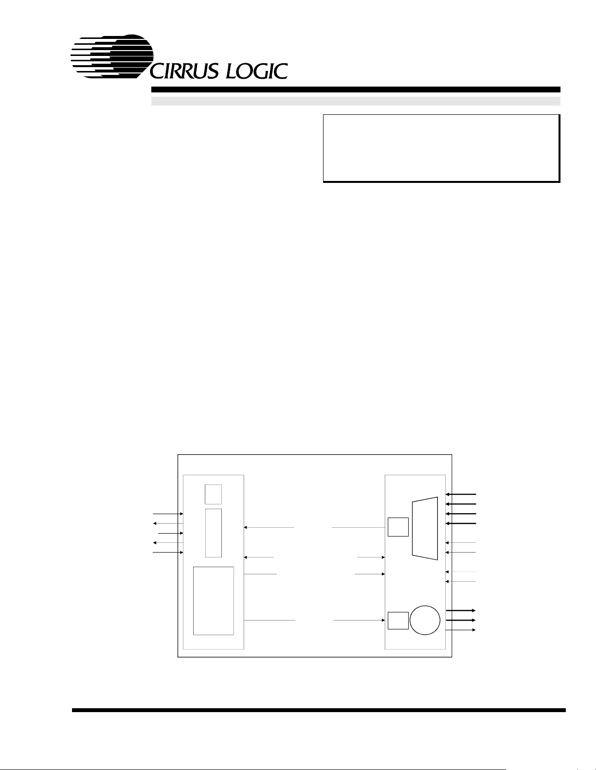
AC-LINK AND AC’97
REGISTERS
PWR
MGT
SYNC
BIT_CLK
SDATA_OUT
SDATA_IN
RESET#
DS242F5 JUN ‘99
AC-
LINK
AC’97
REGISTERS
Copyright Cirrus Logic, Inc. 1999
PCM_DATA
GAIN / MUTE CONTROLS
MIXER / MUX SELECTS
PCM_DATA
(All Rights Reserved)
ANALOG INPUT MUX
AND OUTPUT MIXER
ADC
INPUT
18 bits
MUX
OUTPUT
MIXER
DAC
18 bits
Σ
LINE
CD
AUX
VIDEO
MIC1
MIC2
PHONE
PC_BEEP
LINE_OUT
ALT_LINE_OUT
MONO_OUT

TABLE OF CONTENTS
CHARACTERISTICS AND SPECIFICATIONS.....................................................4
Analog Characteristics .................................................................................4
Mixer Characteristics .. ...... ....... ............................................. ...... ..................5
Absolute Maximum Ratings .........................................................................5
Recommended Operating Conditions..........................................................5
Power Down States......................................................................................6
Digital Filter Characteristics .........................................................................6
Digital Characteristics ..................................................................................7
Serial Port Timing.........................................................................................7
Serial Port Timing.........................................................................................8
PARAMETER AND TERM DEFINITIONS ..........................................................10
GENERAL DESCRIPTION .................................................................................12
Overview ...................................................................................................12
Digital Section ...........................................................................................12
AC-Link ..................... ................................................................. .........12
AC’97 Register Interface .....................................................................12
Power Management ............................................................................12
Analog Section ..........................................................................................12
Output Mixer .......................................................................................12
Input Mux ............................................................................................12
Volume Control ...................................................................................12
AC’97 IMPLEMENTATION ................................................................................13
DIGITAL HARDWARE DESCRIPTION ..............................................................15
AC’97 AC-Link ...........................................................................................15
AC-Link Protocol .................................................................................15
AC-Link Serial Data Output Frame ...........................................................15
Slot 0: Serial Data Output Slot Tags ...................................................16
Slot 1: AC’97 Register Address ..........................................................16
Slot 2: AC’97 Register Write Data ......................................................17
Slot 3: Left Channel PCM Playback Data ...........................................17
Slot 4: Right Channel PCM Playback Data .........................................17
AC-Link Audio Input Frame .......................................................................18
Slot 0: Serial Data Input Slot Tag Bits ................................................18
Slot 1: Read-Back Address Port .........................................................19
Slot 2: Read-Back Data Port ...............................................................19
Slot 3: Left Channel PCM Capture Data .............................................19
Slot 4: Right Channel PCM Capture Data ..........................................20
AC-Link Reset Modes ...............................................................................21
Cold AC’97 Reset ...............................................................................21
Warm AC’97 Reset .............................................................................21
AC’97 Register Reset .........................................................................21
AC-Link Protocol Violation - Loss of SYNC ...............................................21
REGISTER INTERFACE.....................................................................................22
Reset Register (Index 00h) .................................................................23
Master Volume (Index 02h) ................................................................23
Alternate Volume (Index 04h) .............................................................23
Master Mono Volume (Index 06h) ......................................................23
PC_BEEP Volume (Index 0Ah) ..........................................................24
Phone_In Volume (Index 0Ch) ...........................................................24
Microphone Volume (Index 0Eh) ........................................................24
Stereo Analog Mixer Input Gain Registers (Index 10 - 18h) ...............25
CS4297
CrystalClear™ SoundFusion™ Audio Codec ’97
2 DS242F5

CS4297
CrystalClear™ SoundFusion™ Audio Codec ’97
Input Mux Select Register (Index 1Ah) ...............................................25
Record Gain Register (Index 1Ch) .....................................................26
Record Gain Mix (Index 1Eh) .............................................................26
General Purpose Register (Index 20h) ...............................................26
Powerdown Control/Status Register (Index 26h) ...............................27
Reserved Registers (Index 28h - 58h) ................................................27
Crystal Revision and Fab ID Register (Index 5Ah) .............................27
Vendor Reserved Registers (Index 5C - 7Ah) ....................................28
Vendor ID1 (Index 7Ch) .....................................................................28
POWER MANAGEMENT .. ...... ....... ...... ....... ...... ...... ....... ...... ....... ...... ....... ..........29
ANALOG HARDWARE DESCRIPTION ............................................................29
Line-Level Inputs .......................................................................................29
Microphone Level Inputs ...........................................................................30
Mono Inputs ..............................................................................................30
Line Level Outputs ....................................................................................31
Miscellaneous Analo g Signal s ................................................. ....... ...... ....32
Power Supplies .........................................................................................32
GROUNDING AND LAYOUT .............................................................................33
PERFORMANCE PLOTS ...................................................................................34
PIN DESCRIPTIONS...........................................................................................39
Digital I/O Pins ....................................................................................39
Analog I/O Pins ..................................................................................40
Filter and Reference Pins ...................................................................42
Power Supplies ..................................................................................43
REFERENCES ................................................................................................... 43
PACKAGE DIMENSIONS...................................................................................44
Contacting Cirrus Logic Support
For a complete listing of Direct Sales, Distributor, and Sales Representative contacts, visit the Cirrus Logic web site at:
http://www.cirrus.com/corporate/contacts/
Microsoft is a registered trademark of Microsoft Corporation in the United States and/or other countries.
Intel is a registered trademark of Intel Corporation.
Preliminary product info rmation describes products which are i n p r od ucti on, b ut for which full characteriza ti on da t a i s not yet available. Advance product i nf or -
mation describes products which are in development and subject to development changes. Cirrus Logic, Inc. has made best efforts to ensure that the information
contained in this document is accurate and reli able. However , the i nformati on is sub ject to change with out no tice and i s provi ded “AS IS” withou t warranty of
any kind (express or implied). No responsibility is assumed by Cirrus Logic, Inc. for the use of this information, nor for infringements of patents or other rights
of third parties. This document i s the propert y of Cirru s Logic, Inc. and implie s no licen se under patent s, copyri ghts, trademarks, or tr ade secrets. No part of
this publication may be copied, reproduced , stored in a retrieval system, or transmitted, in any form or by any means (electronic, mechanical, photographic, or
otherwise) without the pri or wri tt en consen t of Ci rrus Logic, Inc. Items from any Cirrus Logi c websit e or di sk may be pri nted for use by the user. However, no
part of the printout or electronic files may be copied, reproduced, stored in a retrieval system, or transmitted, in any form or by any means (electronic, mechanical,
photographic, or otherwise) without the prior written consent of Cirrus Logic, Inc.Furthermore, no part of this publication may be used as a basis for manufacture
or sale of any items without the prior written consent of Cirrus Logic, Inc. The names of products of Cirrus Logic, Inc. or other vendors and suppliers appearing
in this document may be trademarks or service marks of their respective owners which may be registered in some jurisdictions. A list of Cirrus Logic, Inc. trademarks and service marks can be found at http://www.cirrus.com.
DS242F5 3
CS4297
CrystalClear™ SoundFusion™ Audio Codec ’97
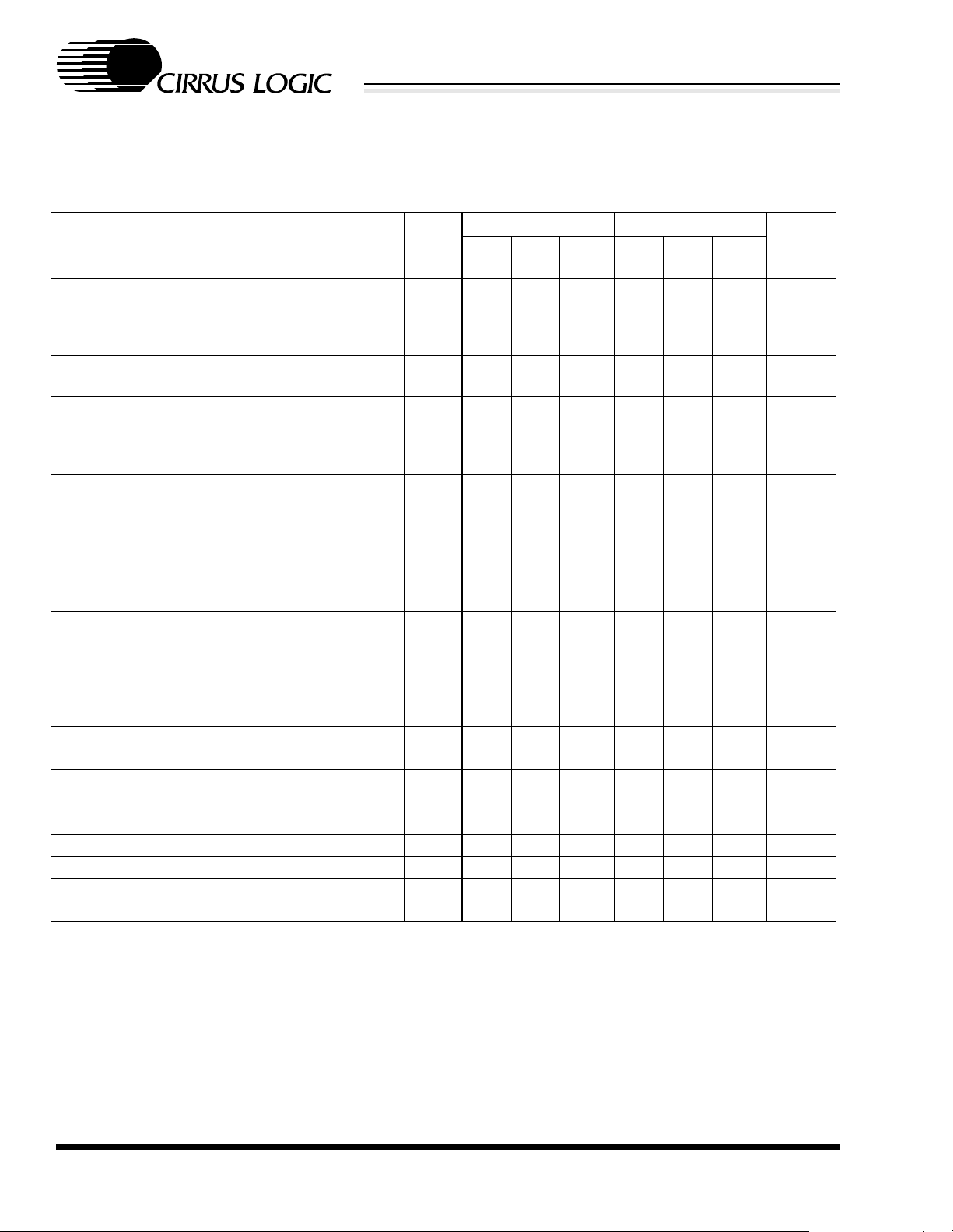
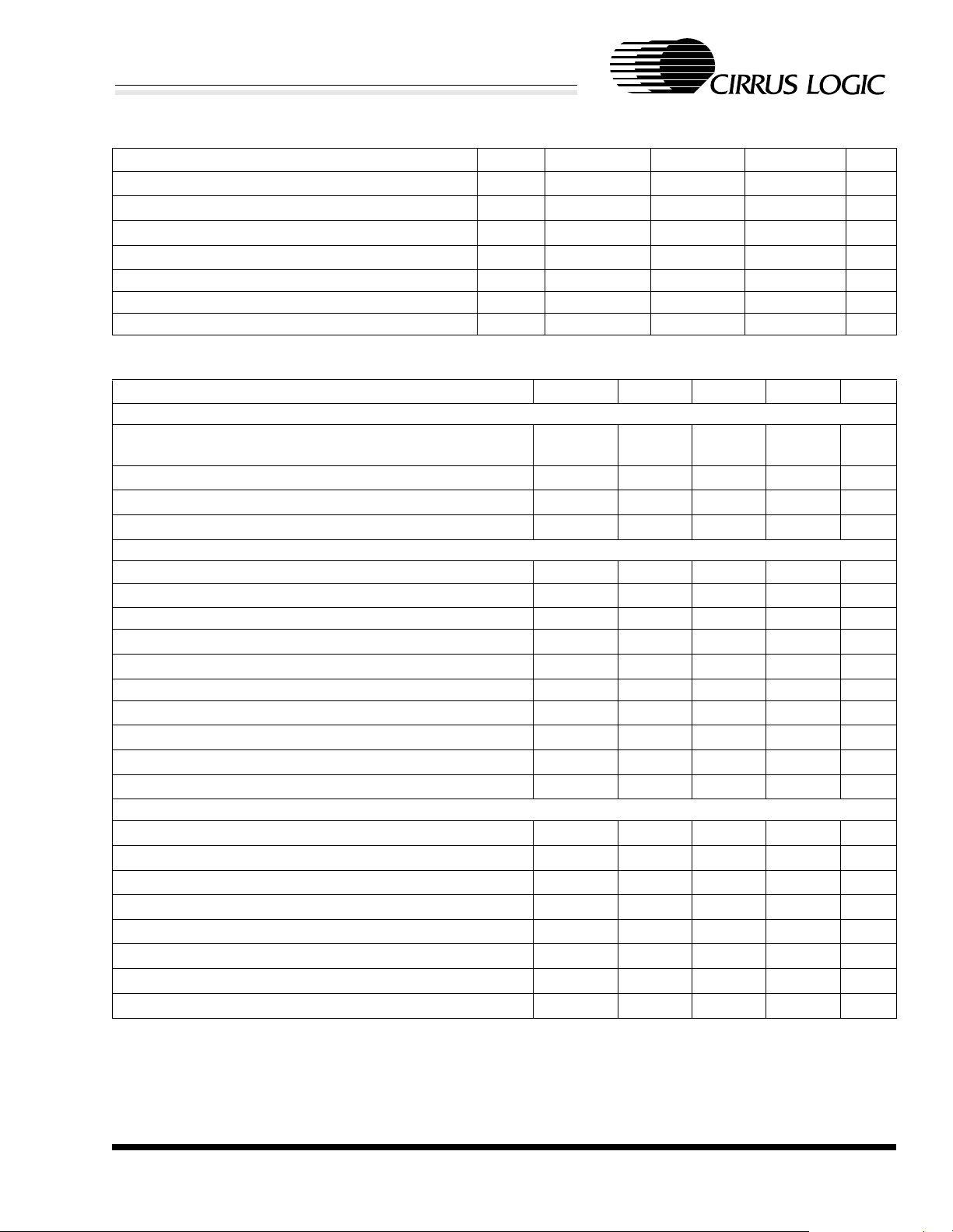
ANALOG CHARACTERISTICS (Standard test conditions unless otherwise noted: T
AVdd = 5.0 V ±5%, DVdd = 3.3 V ±5%; 1 kHz Input Sine wave; Sample Frequency, Fs = 48 kHz; Z
pF load C
= 18 pF load (Note 1); Measurement bandwidth is 20 Hz - 20 kHz, 18-bit linear coding; Mixer registers
DL
= 25° C,
ambient
=10 kΩ/680
AL
set for unity gain.
CS4297-KQ CS4297-JQ
Parameter
(Note 2)
Full Scale Input Voltage
Line Inputs
Mic Inputs (20 dB=0)
Mic Inputs (20 dB=1)
Symbol Path
(Note 3)
A-D
A-D
A-D
0.91
0.91
0.091
1.00
1.00
0.10
UnitMin Typ Max Min Typ Max
V
-
0.91
-
0.91
-
0.091
1.00
1.00
0.10
-
-
-
V
V
RMS
RMS
RMS
Full Scale Output Voltage
Line,Alternate Line, and Mono Outputs D-A 0.91 1.0 1.13 0.91 1.0 1.13
Frequency Response (Note 4)
Analog Ac = ± 0.5 dB
DAC Ac = ± 0.5 dB
ADC Ac = ± 0.5 dB
FR
A-A
D-A
A-D
20
20
20
-
-
-
20,000
20,000
20,000
20
20
20
-
-
-
20,000
20,000
20,000
V
RMS
Hz
Hz
Hz
Dynamic Range
dB FS A
Stereo Analog inputs to LINE_OUT
Mono Analog inputs to LINE_OUT
DAC Dynamic Range
ADC Dynamic Range
DR A-A
A-A
D-A
A-D
90
85
85
85
95
90
90
90
90
-
-
-
-
85
87
85
-
-
-
-
-
dB FS A
dB FS A
dB FS A
DAC SNR (-20 dB FS input w/
CCIR-RMS filter on output) SNR D-A - 63 - - - - dB
Total Harmonic Distortion + Noise
(-3 dB FS input signal):
Line/Alternate Line Output
DAC
ADC (all inputs except phone/mic)
ADC (phone/mic)
THD+N A-A
D-A
A-D
A-D
-94
-
-86
-
-87
-
-87
-
-80
-80
-80
-74
-
-
-
-
dB FS A
-74
dB FS A
-74
dB FS A
-74
-
dB FS A
-74
Power Supply Rejection Ratio
(1 kHz, 0.5 V
w/ 5 V DC offset)(Note 4)
RMS
40 60 - - 40 - dB
Interchannel Isolation 70 87 - - 87 - dB
Spurious Tone (Note 4) - -100 - - -100 - dB FS
Input Impedance (Note 4) 10 - - 10 - - k
External Load Impedance 10 - - 10 - - k
Output Impedance (Note 4) - 730 - - 730 -
Ω
Ω
Ω
Input Capacitance (Note 4) - 5 - - 5 - pF
Vrefout 2.0 2.3 2.5 2.0 2.3 2.5 V
Notes: 1. Z
2. Parameter definitions are given in the
3. Path refers to the signal path used to generate this data. These paths are defined in the
refers to the analog output pin loading and CDL refers to the digital output pin loading.
AL
Term Definitions
Parameter and Term Definitions
section.
section.
Parameter and
4. This specification is guaranteed by silicon characterization, it is not production tested.
4 DS242F5
CS4297
CrystalClear™ SoundFusion™ Audio Codec ’97
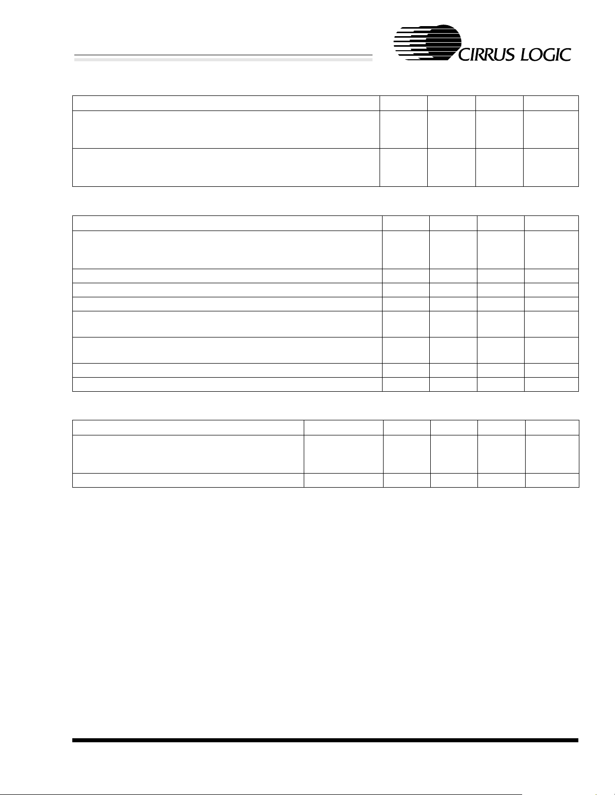
MIXER CHARACTERISTICS (for CS4297-KQ only)
Parameter Min Typ Max Unit
Mixer Gain Range Span
Line In, Aux, CD, Video, Mic1 Mic2, Phone, PC Beep
Line Out, Alternate Line Out, Mono Out
Step Size
All volume controls except PC Beep
PC Beep
-
-
-
-
46.5
94.5
1.5
3.0
-
-
-
-
dB
dB
dB
dB
ABSOLUTE MAXIMUM RATINGS (AVss1 = AVss2 = DVss1 = DVss2 = 0 V)
Parameter Min Typ Max Unit
Power Supplies +3.3 V Digital
+5 V Digital
Analog
Total Power Dissipation (Supplies, Inputs, Outputs) - 210 450 mW
Input Current per Pin (Except Supply Pins) -10 - 10 mA
Output Current per Pin (Except Supply Pins) -15 - 15 mA
Analog Input voltage -0.3 - AVdd+
Digital Input voltage -0.3 - DVdd +
Ambient Temperature (Power Applied) -55 - 110 °C
Storage Temperature -65 - 150 °C
-0.3
-0.3
-0.3
-
-
-
6.0
6.0
6.0
0.3
0.3
V
V
V
V
V
RECOMMENDED OPERATING CONDITIONS (AVss1 = AVss2 = DVss1 = DVss2 = 0 V)
Parameter Symbol Min Typ Max Unit
Power Supplies +3.3 V Digital
+5 V Digital
Analog
Operating Ambient Temperature 0 - 70 °C
DVdd1, DVdd2
DVdd1, DVdd2
AVdd1, AVdd2
3.135
4.75
4.75
3.3
5
5
3.465
5.25
5.25
V
V
V
DS242F5 5
CrystalClear™ SoundFusion™ Audio Codec ’97
POWER DOWN STATES
Parameter Min Typ Max Unit
Full Power 3.3 V digital
5 V digital
5 V analog -
ADCs and Input Mux Powerdown (PR0) 3.3 V digital
5 V digital
5 V analog -
DACs Powerdown (PR1) 3.3 V digital
5 V digital
5 V analog -
Analog Mixer Powerdown, Vref on (PR2) 3.3 V digital
5 V digital
5 V analog -
Analog Mixer Powerdown, Vref off (PR3) 3.3 V digital
5 V digital
5 V analog -
AC-Link Powerdown (PR4) 3.3 V digital
5 V digital
5 V analog -
Internal Clock Disable (PR5) 3.3 V digital
5 V digital
5 V analog -
Alternate Line Output Buffer Powerdown (PR6) 3.3 V digital
5 V digital
5 V analog -
CS4297
12.7
21.4
35.0 - mA
5.32
9.80
23.1 - mA
9.25
16.0
30.0 - mA
9.20
16.0
10.7 - mA
5.30
9.80
~0.00 - mA
3.30
6.92
23.0 - mA
0.004
0.005
0.001 - mA
5.30
9.80
20.3 - mA
DIGITAL FILTER CHARACTERISTICS
CS4297-KQ CS4297-JQ
Parameter
Transition Band
Stop Band
0.4 × F
0.6 × F
-
s
--
s
0.6 × F
0.4 × F
s
0.6 × F
0.6 × F
-
s
-- Hz
s
Stop Band Rejection (Note 4, 5) 74 - - 74 - - dB
Out-of-Band Energy (Note 6) - -82 - - -40 - dB
Group Delay (Note 4) - - 1 - - 1 ms
Notes: 5. Stop Band rejection determines filter requirements. Out-of-band rejection determines audible noise.
6. The integrated Out-of-Band generated by the DAC process, during normal PCM audio playback, over
a bandwidth 28.8 kHz to 100 kHz, with respect to a 1 V
DAC output.
RMS
UnitMin Typ Max Min Typ Max
Hz
s
6 DS242F5
CS4297
CrystalClear™ SoundFusion™ Audio Codec ’97
DIGITAL CHARACTERISTICS (AVss = DVss = 0 V (See
Grounding and Layout
section))
Parameter Symbol Min Typ Max Unit
Low level input voltage
High level input voltage
High level output voltage
Low level output voltage
V
il
V
ih
V
oh
V
ol
- -0.16 x DVddV
0.40 x DVdd - - V
0.70 x DVdd 0.99 x DVdd - V
- 0.03 0.10 x DVdd V
Input Leakage Current (AC-link inputs) -10 - 10 µA
Output Leakage Current (Tri-stated AC-link outputs) -10 - 10 µA
Output buffer drive current (Note 4) - 100 400 µA
SERIAL PORT TIMING
Parameter Symbol Min Typ Max Unit
RESET Timing
DVdd 90% maximum value to RESET# inactive pre-delay
(Note 4)
RESET# active low pulse width
RESET# inactive to BIT_CLK start-up delay
1st SYNC active to CODEC READY set
Clocks
BIT_CLK frequency - 12.288 - MHz
BIT_CLK period
BIT_CLK output jitter (depends on XTAL_IN source) - - 750 ps
BIT_CLK high pulse width
BIT_CLK low pulse width
SYNC frequency - 48 - kHz
SYNC period
SYNC high pulse width
SYNC low pulse width
SYNC active to RESET# inactive pre-delay
Data Setup and Hold
Output Propagation delay from rising edge of BIT_CLK
Output hold from falling edge of BIT_CLK
Input setup time from falling edge of BIT_CLK
Input hold time from falling edge of BIT_CLK
Input Signal rise time
Input Signal fall time
Output Signal rise time (Note 4)
Output Signal fall time (Note 4)
T
Vdd2rst#
T
rst_low
T
rst2clk
T
sync2crd
T
clk_period
T
clk_high
T
clk_low
T
sync_period
T
sync_high
T
sync_low
T
rst2snyc
T
prop
T
ohold
T
isetup
T
ihold
T
irise
T
ifall
T
ofall
T
ofall
1.5 - - ms
1.0 - -
µ
- 42.7 - ms
- 40.6 -
µ
- 81.4 - ns
- 40.7 - ns
- 40.7 - ns
- 20.8 -
µ
-1.3-µs
- 19.5 -
µ
- - 250 ms
-68ns
5--ns
10 - - ns
0--ns
2-6ns
2-6ns
246ns
246ns
s
s
s
s
DS242F5 7
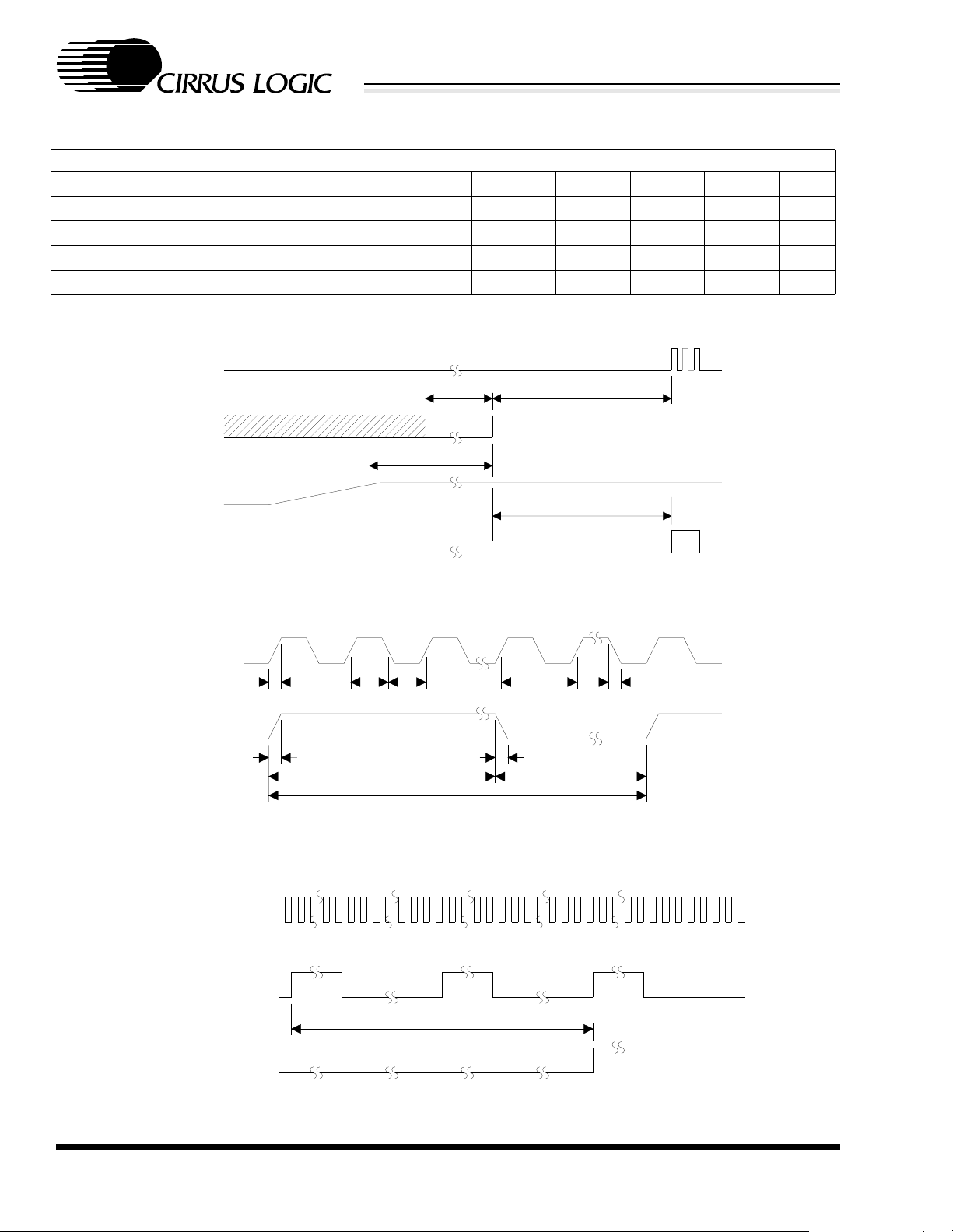
SERIAL PORT TIMING (Continued)
Misc. Timing Parameters
End of Slot 2 to BIT_CLK, SDATA_IN low (PR4)
SYNC pulse width (PR4)
SYNC inactive (PR4) to BIT_CLK start-up delay
Setup to trailing edge of RESET# (test modes) (Note 4)
Rising edge of RESET# to Hi-Z delay (Note 4)
BIT_CLK
T
rst_low
RESET#
T
vdd2rst#
CS4297
CrystalClear™ SoundFusion™ Audio Codec ’97
T
s2_pdown
T
sync_pr4
T
sync2clk
T
setup2rst
T
off
- 16.24 16.36
1.0 - -
162.8 244 - ns
15 - - ns
- - 25 ns
T
rst2clk
µ
s
µ
s
Vdd
SYNC
BIT_CLK
SYNC
BIT_CLK
T
T
orise
irise
Power Up Timing
T
clk_highTclk_low
T
sync_high
T
T
ifall
sync_period
Clocks
T
clk_period
T
T
rst2sync
sync_low
T
ifall
SYNC
T
sync2crd
CODEC_READY
Codec Ready from Startup or Fault C on di t i on
8 DS242F5
CS4297
CrystalClear™ SoundFusion™ Audio Codec ’97
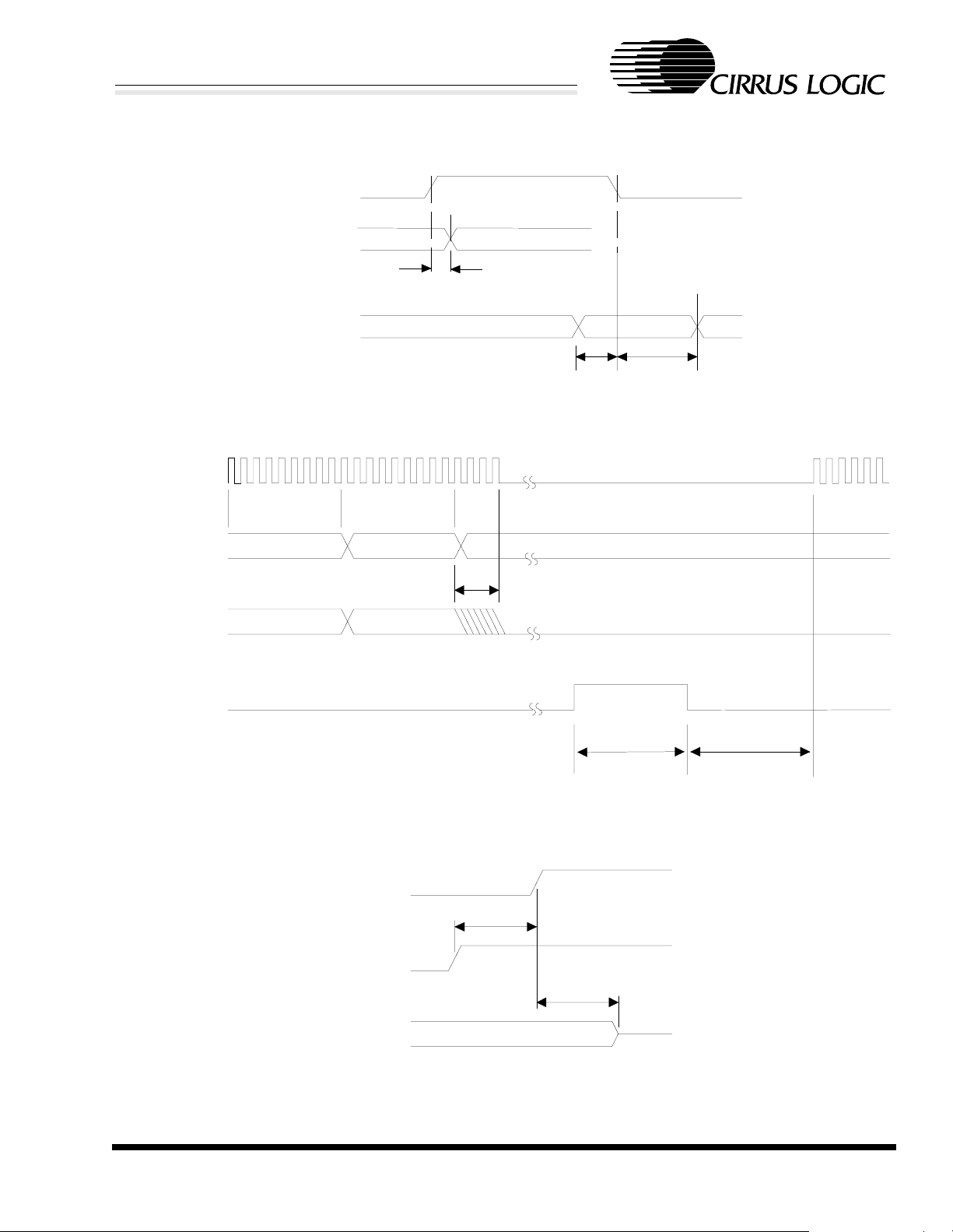
BIT_CLK
SDATA_IN
T
co
SDATA_OUT,
SYNC
Data Setup and Hold
BIT_CLK
T
setup
T
hold
SDATA_OUT
SDATA_IN
SYNC
Slot 1 Slot 2
Write to 0x20 Data PR4 Don’t Care
T
s2_pdown
T
PR4 Powerdown
RESET#
T
setup2rst
SDATA_OUT,
SYNC
T
off
sync_pr4
T
sync2clk
SDATA_IN,
Hi-Z
BIT_CLK
Test Mode
DS242F5 9

PARAMETER AND TERM DEFINITIONS
AC’97 Specification
Refers to the Audio Codec ‘97 Component Specification Ver 1.03 published by Intel
Corporation [1].
AC’97 Controller
Refers to the control chip which interfaces to the CS4297’s AC-Link. This has been also called
“DC’97” [1].
‘set’
Refers to a digital value of Vcc, “1”, or “high”.
‘clear’ or ‘cleared’
Refers to a digital value of GND, “0” or “low”.
AC’97 Registers
CS4297
CrystalClear™ SoundFusion™ Audio Codec ’97
®
Refers to the 64-field register map defined in the AC’97 Specification.
ADC
Refers to a single Analog-to-Digital converter in the CS4297. “A DCs” refers to the stereo pair
of Analog-to-Digital converters.
DAC
A single Digital-to-Analog converter in the CS4297. “DACs” refers to the stereo pair of
Digital-to-Analog converters.
Codec
Refers to the set of ADCs, DACs, and Analog mixer portions of the CS4297.
FFT
Fast Fourier Transform.
Resolution
The number of bits in the output words to the DACs, and in the input words to the ADCs.
Differential Nonlinearity
The worst case deviation from the ideal code width. Units in LSB.
dB FS A
dB FS is defined as dB relative to full-scale. The “A” indicates an A weighting filter was used.
10 DS242F5

CS4297
CrystalClear™ SoundFusion™ Audio Codec ’97
Frequency Response (FR)
FR is the deviation in signal level verses frequency. The 0 dB reference point is 1 kHz. The
amplitude corner, Ac, lists the maximum deviation in amplitude above and below the 1 kHz
reference point. The listed minimum and maximum frequencies are guaranteed to be within the
Ac from minimum frequency to maximum frequency inclusive.
Dynamic Range (DR)
DR is the ratio of the RMS full-scale signal level divided by the RMS sum of the noise floor,
in the presence of a signal, available at any instant in time (no change in gain settings between
measurements). Measured over a 20 Hz to 20 kHz bandwidth with units in dB FS A.
Total Harmonic Distortion plus Noise (THD+N)
THD+N is the ratio of the RMS sum of a ll non-fundamental frequency components, divided by
the RMS full-scale signal level. It is tested using a -3 dB FS input signal and is measured over
a 20 Hz to 20 kHz bandwidth with units in dB FS A.
Signal to Noise Ratio (SNR)
SNR, similar to DR, is the ratio of an arbitrary sinusoidal input signal to the RMS sum of the
noise floor, in the presence of a signal. It is measured over a 20 Hz to 20 kHz bandwidth with
units in dB.
Interchannel Isolation
The amount of 1 kHz signal present on the output of the grounded AC-coupled line input
channel with 1 kHz 0 dB signal present on the other line input channel. Units in dB.
Interchannel Gain Mismatch
For the ADCs, the difference in input voltage to get and equal code on both channels. For the
DACs, the difference in output voltages for each channel when both channels are fed the same
code. Units in dB.
PAT HS : [4 ]
A-D: Analog in, through the ADC, onto the serial link.
D-A: Serial interface inputs through the DAC to the analog output
A-A: Analog in to Analog out (analog mixer)
DS242F5 11

CS4297
CrystalClear™ SoundFusion™ Audio Codec ’97
GENERAL DESCRIPTION
Overview
The CS4297 is a mixed-signal serial Codec based
on the AC’97 Specification. It is designed to be
paired with a digital controller, typically located on
the PCI bus. The AC’97 Controller is responsible
for all communications between the CS4297 and
the rest of the system. The CS4297 functions as an
analog mixer, a stereo ADC, a stereo DAC, and a
control and digital audio stream interface to the
AC’97 Controller.
The CS4297 contains two distinct functional sections: Digital and Analog. The Digital section includes the AC-Link registers, power management
support, SYNC detection circuitry, and AC-Link
serial port interface logic. The Analog section includes the analog input multiplexor (mux), stereo
output mixer, mono output mixer, stereo ADCs,
stereo DACs, and analog volume controls.
Digital Section
AC-Link
The AC-Link is the 5-wire digital interface to the
AC’97 Controller chip. The CS4297 generates the
BIT_CLK and the SDATA_IN signals. The AC’97
Controller must drive the SYNC, SDATA_OUT
and RESET# signals. Please refer to the AC-Link
timing section for the timing characteristics of the
interface. The interface uses the SYNC signal,
which is synchronous with BIT_CLK, to align the
data within the frame. The AC-Link signals may be
referenced to either 5 Volts or 3.3 Volts. The
CS4297 should use the same digital supply voltage
as the AC’97 Controller chip.
AC’97 Register Interface
The CS4297 implements the AC’97 Registers in
accordance with the AC’97 Specification. See the
Register Interface section for details on the
CS4297’s register set.
Power Management
The CS4297 supports a number of different power
down modes. They are accessed through register
0x26h of the CS4297 register interface. Please refer
to the Power Management section of the data sheet.
Analog Section
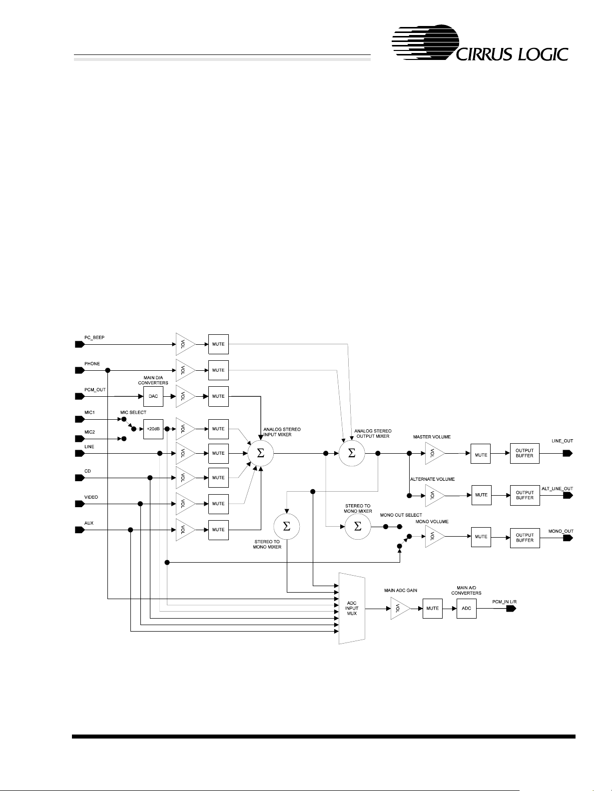
Please refer to Figure 1, Mixer diagram, for a high
level graphical representation of the CS4297 analog mixer structure.
Output Mixer
There are two output mixers on the CS4297. The
stereo output mixer sums together the analog inputs
to the CS4297 according to the settings in the volume control registers. The mono output mixer generates a monophonic sum of the left and right
channels from the stereo output mixer. However,
the mono output mixer does not include the
PC_BEEP and PHONE signals which are included
in the stereo output mix. The stereo output mix is
sent to the LINE_OUT and ALT_LINE_OUT output pins of the CS4297. The mono output mix is
sent to the MONO_OUT output pin on the CS4297.
Input Mux
The input multiplexor controls which analog input
is sent to the ADCs. The output of the input mux is
converted to stereo 18-bit digital PCM data and
sent to the AC’97 Controller chip in Slots 3 and 4
of the AC-Link SDATA_IN signal.
Volume Control
The volume control registers of the AC’97 Register
interface control analog input level to the input
mixer, the master volume level, and the alternate
12 DS242F5
CS4297
CrystalClear™ SoundFusion™ Audio Codec ’97
volume level. All analog volume controls, except
PC_BEEP, implement controlled volume steps at
nominally 1.5 dB per step. PC_BEEP uses 3 dB
steps. The analog inputs allow a mixing range of
+12 dB of signal gain to -34.5 dB of signal a ttenuation. The analog output volume controls allow
from 0 dB to -94.5 dB of attenuation. The
PC_BEEP input volume control allows from 0 dB
to -45 dB of attenuation.
AC’97 IMPLEMENTATION
The CS4297 implements an AC’97 compliant design as defined in the Intel Audio Codec 97 Specification Version 1.03. Due to certain design tradeoffs and implementation decisions, the CS4297 dif-
fers from the AC’97 Specification in a a few minor
ways. The following list captures the specification
deviations and the implementation decisions made
to resolve ambiguities.
1. The rising edge of RESET# must occur at least
1.5 ms after the digital power supply DVdd reaches
90% of maximum value.
2. The digital input voltage threshold levels are
specified as percentages of the Vdd digital power
supply and are TTL level compatible. Min Vih =
0.4 x Vdd, Max Vil = 0.16 x Vdd.
3. The delay between setting the PR4 bit to powering down the AC-Link interface is implemented as
16.24 µs.
Figure 1. Mixer Diagram
DS242F5 13

CS4297
CrystalClear™ SoundFusion™ Audio Codec ’97
4. The digital outputs are specified with a 18 pF capacitive load.
5. The nominal Vrefout level is 2.2 V.
6. All analog mixer input and output paths are designed to achieve greater than 90 dBFSA Dynamic
Range.
7. All stereo-to-mono mixer stages contain a scale
factor of -6 dB to prevent output clipping of the
summed mono signal.
8. When the analog mixer is powered down, the
control registers for Record Select and Record
Gain are frozen. The analog mixer stage must be
powered up to gain access to these registers.
9. The Headphone Output pins have been implemented as an Alternate Line Output. These pins
must drive loads greater than 10 kΩ, just as the
Line Outputs.
10. Reserved bits in the AC’97 serial data input
stream may return a ‘set’ or a ‘cleared’ value.
11. The Vref pin defined in the AC’97 Specification has been renamed to REFFLT. This pin is used
for internal filtering and should not be used as an
external circuit bias voltage. The Vrefout pin is
used to supply biasing voltages to external analog
circuitry. This pin is not capable of supplying 5 mA
of bias current as the specification indicates.
14 DS242F5

CS4297
CrystalClear™ SoundFusion™ Audio Codec ’97
DIGITAL HARDWARE DESCRIPTION
AC’97 AC-Link
The AC-Link is the seri al connection between the
AC’97 Controller and the CS4297. The interface
consists of 5 signal lines (2 data, 2 clocks, and 1 reset). The basic connections of the link are shown in
Figure 2. The signals will be explained in detail below.
AC-Link Protocol
The CS4297 serial interface is designed according
to the AC’97 Specification to allow connection to
any AC’97 Controller. An AC-Link audio frame is
divided into 13 ‘slots’; 1 16-bit slot and 12 20-bit
slots. During each audio frame, data is passed bi-directionally between the CS4297 and the AC’97
Controller.
AC-Link Serial Data Output Frame
For the serial data output frame, the SYNC,
BIT_CLK, and SDATA_OUT signals are used. In
the serial data output frame, data is passed on the
SDATA_OUT pin FROM the AC’97 Controller
TO the CS4297. In Figure 3 and in the following
Frame Slot definitions, the position of each bit location within the frame is noted. The first bit posi-
tion in a new serial data frame is F0 and the last bit
position in the serial data frame is F255.
When SYNC goes active (high) and is sampled active by the CS4297 (on the falling edge of
BIT_CLK), both devices are synchronized to a new
serial data frame. The data on the SDATA_OUT
pin at this clock edge is the final bit of the previous
serial data frame’s data. On the next rising edge of
BIT_CLK, the first bit of slot 0 is driven by the
AC’97 Controller on the SDATA_OUT pin. The
CS4297 latches in this data, as the first bit of the
frame, on the next falling edge of the BIT_CLK
clock signal.
Digit al AC ’9 7
Controller CS4297
SY NC
BI T_CLK
SDATA_OU T
SDATA_I N
RESET #
Figure 2. AC-link Connections
20.8uS
(48 KHz)
F37 F57
LP17 LP16 RP17
LC17 LC16 RC17RD15 RD1400000
F97
F97
X
0
F255
F255
0
SYNC
BIT_CLK
Bit Frame
Position
SDATA_OUT
Bit Frame
Posit i o n
SDATA_IN
Tag Phase Data Phase
12.288 MHz
81.4 nS
F0 F1 F2 F16F15F14F13F12 F36 F56 F76
F255
Valid
Slot 1
X X
Frame
F0 F1 F2 F16F15F14F13F12 F36 F56 F76F255 F37 F57
Codec
0
Ready
Valid
Slot 1
Valid
Slot 2
Valid
Slot 2
Valid
X X X X R/W WD15 WD14
Slot 0 Slot 1 Slot 2 Slot 3 Slot 4 Slots 5-12
Figure 3. AC-Link Input and Output Framing
DS242F5 15

CS4297
CrystalClear™ SoundFusion™ Audio Codec ’97
Slot 0: Serial Data Output Slot Tags
The first slot, Slot 0, is a 16-bit slot which contains information about the validity of data for the remaining
12 slots. The 16 bits of this slot are defined as:
F0 F1 F2 F3 F4 F5 F6 F7 F8 F9 F10 F11 F12 F13 F14 F15
Bit 1514131211109876543210
Valid
Slot 1
Frame
Valid
Valid Frame - Bit 15 determines if any of the following slots contain valid data. If this bit is ‘set’, at least
one of the other 12 slots contain valid data. If this bit is ‘cleared’, the remainder of the frame will be ignored.
Slot 1 Valid - Bit 14 indicates the validity of data in the serial data output Slot 1. If this bit is ‘set’, Slot 1
contains valid data. If this bit is ‘cleared’, Slot 1 will be ignored.
Slot 2 Valid - Bit 13 indicates the validity of data in the serial data output Slot 2. If this bit is ‘set’, Slot 2
contains valid data. If this bit is ‘cleared’, Slot 2 will be ignored.
Slot 3 Valid - Bit 12 indicates the validity of data in the serial data output Slot 3. If this bit is ‘set’, Slot 3
contains valid data. If this bit is ‘cleared’, Slot 3 will be ignored.
Slot 2
Valid
Slot 3
Valid
Slot 4
Valid
Not Used
Slot 4 Valid - Bit 11 indicates the validity of data in the serial data output Slot 4. If this bit is ‘set’, Slot 4
contains valid data. If this bit is ‘cleared’, Slot 4 will be ignored.
Slot 0 bits 10 through 0 represent unimplemented data slots in the CS4297 and will be ignored.
The input PCM data to the CS4297 on the SDATA_OUT pin is shifted out MSB justified (most significant
bit of the actual data of the 20-bit slots). In any case where there are less than 20-bits of valid data for a
slot (i.e.: 18-bit PCM data in a 20-bit slot), the trailing bit s of the slot must be ‘cleared’ by the AC’97 Controller. For Slots 5 - 12, the AC’97 Controller should ‘clear’ each bit in each frame, however data in these
slots will be ignored.
Slot 1: AC’97 Register Address
Slot 1 indicates the Register Address of the current frame’s register access. The 20 bits of this slot are defined as:
F16 F17 F18 F19 F20 F21 F22 F23 F24 F25 F26 F27 F28 F29 F30 F31 F32 F33 F34 F35
Bit 191817161514131211109876543210
R/W
RI6 RI5 RI4 RI3 RI2 RI1 RI0 Reserved
Table 1. Command Address Port Bit Definition
R/W - Bit 19 is the Read/Write bit. When this bit is ‘set’, a read of the AC’97 Register specified by the
Register Index will occur. When the bit is ‘cleare d’, a write will occur. In both cases, register ac cesses only
occur when the Slot Valid bit 14 of Slot 0 (F1) corresponding to Slot 1 is ‘set’.
RI6 - RI0 - Bits 18-12 contain the 7-bit register index to the AC’97 Registers in the CS4297. All registers
are defined at word addressable boundarie s. Bit 12 will be save d for his toric purposes but is not dec oded.
Bits 11-0 are reserved and should always be ‘cleared’ the AC’97 Controller.
16 DS242F5

CS4297
CrystalClear™ SoundFusion™ Audio Codec ’97
Slot 2: AC’97 Register Write Data
Slot 2 indicates the Register Data of the current frame’s register write access.The 20 bits of this slot are
defined as:
F36 F37 F38 F39 F40 F41 F42 F43 F44 F45 F46 F47 F48 F49 F50 F51 F52 F53 F54 F55
Bit 191817161514131211109876543210
WD15 WD14 WD13 WD12 WD11 WD10 WD9 WD8 WD7 WD6 WD5 WD4 WD3 WD2 WD1 WD0 Reserved
WD15 - WD0 - Bits 19-4 contain the 16-bit value to be written to the register. Bits 3-0 are ignored, but
should always be ‘cleared’. If the access is a read, this slot is ignored. The data in Slot 2 will only be valid
when the Slot Valid bit 13 of Slot 0 (F2) corresponding to Slot 2 is ‘set’.
NOTE: For any write to an AC’97 Register, the write is defined to be an ‘atomic’ access. This mea ns that
when the slot valid bit for Slot 1 is ‘set’, the slot valid bit for Slot 2 should always be ‘set’ during the same
audio frame. No write access may be split across 2 frames.
Slot 3: Left Channel PCM Playback Data
Slot 3 contains the left channel data. The 20 bits of this slot are defined as:
F56 F57 F58 F59 F60 F61 F62 F63 F64 F65 F66 F67 F68 F69 F70 F71 F72 F73 F74 F75
Bit 191817161514131211109876543210
LP17 LP16 LP15 LP14 LP13 LP12 LP11 LP10 LP9 LP8 LP7 LP6 LP5 LP4 LP3 LP2 LP1 LP0 Reserved
LP17 - LP0 - This is the 18-bit PCM playback 2’s compliment data for the left channel DAC in the
CS4297. The PCM playback data will be taken from the m ost significant 18 of the 20 bit s in the slot. The
least significant 2 bits will be ignored. Any PCM data from the AC’97 Controller that is not at least 18bits should be left justified in Slot 3 and dithered or zero-padded in the unused bit positions.
Slot 4: Right Channel PCM Playback Data
Slot 4 contains the right channel data. The 20 bits of this slot are defined as:
F76 F77 F78 F79 F80 F81 F82 F83 F84 F85 F86 F87 F88 F89 F90 F91 F92 F93 F94 F95
Bit 191817161514131211109876543210
RP17 RP16 RP15 RP14 RP13 RP12 RP11 RP10 RP9 RP8 RP7 RP6 RP5 RP4 RP3 RP2 RP1 RP0 Reserved
RP17 - RP0 - This is the 18-bit PCM playback 2’s compliment data for the right channel DAC in the
CS4297. The PCM playback data will be taken from the m ost significant 18 of the 20 bit s i n the slot. The
least significant 2 bits will be ignored. Any PCM data from the AC’97 Controller that is not at least 18bits should be left justified in Slot 4 and dithered or zero-padded in the unused bit positions.
DS242F5 17

CS4297
CrystalClear™ SoundFusion™ Audio Codec ’97
AC-Link Audio Input Frame
An AC-Link serial data input frame uses the
SYNC, BIT_CLK, and SDATA_IN signals are
used. In the serial data input frame, data is passed
on the SDATA_IN pin FROM the CS4297 TO the
AC’97 Controller. The data format for the input
frame is very similar to the output frame. Synchronization of the CS4297 to the AC’97 Controller is
performed in the same manner. Please refer to Figure 3 for the serial port timing waveform.
Slot 0: Serial Data Input Slot Tag Bits
The first slot, Slot 0, is a 16-bit slot which contains information about the validity of data for the remaining
12 slots. The 16 bits of this slot are defined as:
F0 F1 F2 F3 F4 F5 F6 F7 F8 F9 F10 F11 F12 F13 F14 F15
Bit 1514131211109876543210
Codec
Ready
Slot 1
Valid
Slot 2
Valid
Slot 3
Valid
Slot 4
Valid
Not Used
Codec Ready - Bit 15 indicates the readiness of the CS4297’s AC-Link and the AC’97 Control and Status
Registers. Immediately after a Cold Reset this bit will be returned to the AC’97 C ontroller ‘cleared’. Once
the CS4297’s clocks and voltages are stable, this bit will be set. Until the Codec R eady bit is ‘set’, no ACLink transactions should be attempted by the AC’97 Controller.
NOTE: This Codec Ready bit does not indicate readiness of the DACs, ADCs, Vref, or any other analog
function. Those must be checked in the Powerdown/Status Register by the AC’97 Controller. Any accesses
to the CS4297 while this bit is ‘cleared’ will be ignored.
Slot 1 Valid - Bit 14 indicates the validity of data in the serial data input Slot 1. If this bit is ‘set’, Slot 1
contains valid data. If this bit is ‘cleared’, Slot 1 should be ignored by the AC’97 Controller.
Slot 2 Valid - Bit 13 indicates the validity of data in the serial data input Slot 2. If this bit is ‘set’, Slot 2
contains valid data. If this bit is ‘cleared’, Slot 2 should be ignored by the AC’97 Controller.
Slot 3 Valid - Bit 12 indicates the validity of data in the serial data input Slot 3. If this bit is ‘set’, Slot 3
contains valid data. If this bit is ‘cleared’, Slot 3 should be ignored by the AC’97 Controller.
Slot 4 Valid - Bit 11 indicates the validity of data in the serial data input Slot 4. If this bit is ‘set’, Slot 4
contains valid data. If this bit is ‘cleared’, Slot 4 should be ignored by the AC’97 Controller.
Slot 0 bits 10 through 0 represent unimplemented data slots in the CS4297 and should be ignored by the
AC’97 Controller.
18 DS242F5

CS4297
CrystalClear™ SoundFusion™ Audio Codec ’97
Slot 1: Read-Back Address Port
Slot 1 is the Read-Back Address Port. The Read-Back Address Port is used to echo the AC’97 Register
address back to the AC’97 Controller when the CS4297 has been issued a read request from the previous
frame. Included only for historical purposes, this address may be used by the AC’97 Controller to synchronize read accesses. The CS4297 will only echo the register index for a read access. Write accesses will not
return valid data in Slot 1. The 20 bits of this slot are defined as:
F16 F17 F18 F19 F20 F21 F22 F23 F24 F25 F26 F27 F28 F29 F30 F31 F32 F33 F34 F35
Bit 191817161514131211109876543210
0RI6RI5RI4RI3RI2RI1RI0000000000000
RI6 - RI0 - Bits 18-12 contain the 7-bit register index to the AC’97 Registers in the CS4297.
All other undefined bits in Slot 1 will be returned by the CS4297 ‘cleared’.
Slot 2: Read-Back Data Port
Slot 2 is the Read-Back Data Port. The Read-Back Data Port contains the register data requested by the
AC’97 Controller from the previous read request. It reflects the valid data bits from the 16-bit AC’97 Register being read. All read requests will return read addresses and data on the following serial data frame.
The 20 bits of this slot are defined as:
F36 F37 F38 F39 F40 F41 F42 F43 F44 F45 F46 F47 F48 F49 F50 F51 F52 F53 F54 F55
Bit 191817161514131211109876543210
RD15 RD14 RD13 RD12 RD11 RD10 RD9 RD8 RD7 RD6 RD5 RD4 RD3 RD2 RD1 RD0 0 0 0 0
WD15 - WD0 - Bits 19-4 contain the 16-bit AC’97 Register value returned to the AC’97 Controller by the
CS4297. Bits 3-0 are undefined in Slot 2 and will be returned by the CS4297 ‘cleared’.
NOTE: The CS4297 implements bus-keeper logic for its 16-bit registers. Any read accesses from AC’97
Registers with undefined bits may return a ‘set’ or ‘clear’ value. The value returned depends on the state
of that bit location from the previous access. No AC’97 Controller software dependencies should exist on
the value of undefined AC’97 Register bits. For a list of the undefined bits in the AC’97 register map, see
Table 2, Mixer Registers.
Slot 3: Left Channel PCM Capture Data
Slot 3 contains the left channel data. The 20 bits of this slot are defined as:
F56 F57 F58 F59 F60 F61 F62 F63 F64 F65 F66 F67 F68 F69 F70 F71 F72 F73 F74 F75
Bit 191817161514131211109876543210
LP17 LP16 LP15 LP14 LP13 LP12 LP11 LP10 LP9 LP8 LP7 LP6 LP5 LP4 LP3 LP2 LP1 LP0 0 0
LP17 - LP0 - This is the 18-bit PCM 2’s compliment capture data from the left channel ADC in the
CS4297. The PCM capture data is left justified in the most significant 18 of the 20 bits in the slot.
The least significant 2 bits will be ‘cleared’.
DS242F5 19

CS4297
CrystalClear™ SoundFusion™ Audio Codec ’97
Slot 4: Right Channel PCM Capture Data
Slot 4 contains the right channel data. The 20 bits of this slot are defined as:
F76 F77 F78 F79 F80 F81 F82 F83 F84 F85 F86 F87 F88 F89 F90 F91 F92 F93 F94 F95
Bit 191817161514131211109876543210
RP17 RP16 RP15 RP14 RP13 RP12 RP11 RP10 RP9 RP8 RP7 RP6 RP5 RP4 RP3 RP2 RP1 RP0 0 0
RP17 - RP0 - This is the 18-bit PCM 2’s compliment capture data from the right channel ADC in the
CS4297. The PCM capture data is left justified in the most significant 18 of the 20 bits in the slot.
The least significant 2 bits will be ‘cleared’.
Slots 5 through 12 are not implemented in the CS4297, and t herefore will always be returned ‘cleared’ for
all bits.
20 DS242F5

CS4297
CrystalClear™ SoundFusion™ Audio Codec ’97
AC-Link Reset Modes
There are 3 methods to reset the CS4297. These are
defined in the AC’97 Specification as ‘Cold AC’97
Reset’, ‘Warm AC’97 Reset’, and AC’97 Register
Reset. A ‘Cold AC’97 Reset’ is required to restart
the AC-Link when bit PR5 is ‘set’ in register
(0x26).
Cold AC’97 Reset
A Cold Reset is performed simply by asserting RESET# in accordance with the minimum timing
specifications in the Serial Port Timing section of
the data sheet. Once de-asserted, all of the AC’97
Registers will be reset to their default power-on
states and the BIT_CLK clock and SDATA_IN
signals will be reactivated. The timing of powerup/reset events is discussed in detail in the Power
Management section of the data sheet.
Warm AC’97 Reset
AC’97 Register Reset
The third reset mode provides a register reset to the
CS4297. This is available only when the CS4297’s
AC-Link is active and the Codec Ready bit is ‘set’.
The Register Reset allows all user accessible registers in the CS4297 to be reset to their default, power-up values. A Register Reset occurs when any
value is written to AC’97 Register 00h.
AC-Link Protocol Violation - Loss of SYNC
The CS4297 was designed to handle SYNC protocol violations. The following are situations where
the SYNC protocol has been violated:
The SYNC signal is not sampled high for exactly
16 BIT_CLK clock cycles at the start of an audio
frame.
The SYNC signal is not sampled high on the 256th
BIT_CLK clock period after the previous SYNC
assertion.
The CS4297 may also be reactivated when the ACLink is powered down (refer to the PR4 bit description in the Power Management section of the data
sheet) by a Warm Reset. A Warm Reset allows the
AC-Link to be reactivated without losing informa-
tion in the AC’97 Registers. Warm Reset is initiated when the SYNC signal is driven high for at least
1 µs and then driven low in the absence of the
BIT_CLK clock signal. The BIT_CLK clock will
not restart until at least 2 normal BIT_CLK clock
periods (± 162.8 ns) after the SYNC signal is de-asserted.
The SYNC signal goes active high before the 256th
BIT_CLK clock period after the previous SYNC
assertion.
Upon loss of synchronization with the AC’97 Controller, the CS4297 will mute all analog outputs and
‘clear’ the Codec Ready bit in the serial data input
frame until 2 valid frames are detected. During this
detection period, the CS4297 will ignore all register reads and writes and will discontinue the transmission of PCM capture data.
DS242F5 21

REGISTER INTERFACE
CS4297
CrystalClear™ SoundFusion™ Audio Codec ’97
Reg
Num
00h Reset 0 0 0 0 0 0 0 1 0 1 0 1 0 0 0 0 0150h
02h Master Volume Mute X ML5 ML4 ML3 ML2 ML1 ML0 X X MR5 MR4 MR3 MR2 M R1 MR0 8000h
04h Alternat e L ine Out Volume Mute X ML5 ML4 ML3 ML2 ML1 ML0 X X MR5 MR4 MR3 MR2 MR1 MR0 8000h
06h Master Volume Mono Mute X X X X X X X X X MM5 MM4 MM3 MM2 MM1 MM0 8000h
08h Reserve d 0 0 0 0 0 0 0 0 0 0 0 0 0 0 0 0 0000h
0Ah PC_BEEP Volume Mute X X X X X X X X X X PV3 PV2 PV1 PV0 X 0000h
0Ch Phone Volume Mute X X X X X X X X X X GN4 G N3 GN2 GN1 GN0 8008h
0Eh Mic Volume Mute X X X X X X X X 20dB X GN4 GN3 GN2 GN1 GN0 8008h
10h Line In Volume Mute X X GL4 GL3 GL2 GL1 GL0 X X X GR4 GR3 GR2 GR1 GR0 8808h
12h CD Volume Mute X X GL4 GL3 GL2 GL1 GL0 X X X GR4 GR3 GR2 GR1 GR0 8808h
14h Video Volume Mute X X GL4 GL3 GL2 GL1 GL0 X X X GR4 GR3 GR2 GR1 GR0 8808h
16h Aux Volume Mute X X GL4 GL3 GL2 GL1 GL0 X X X GR4 GR3 GR2 GR1 GR0 8808h
18h PCM Out Vol Mute X X GL4 GL3 GL2 GL1 GL0 X X X GR4 GR3 GR2 GR1 GR0 8808h
1Ah Record Select X X X X X SL2 SL1 SL0 X X X X X SR2 SR1 SR0 0000h
1Ch Record Gain Mute X X X GL3 GL2 GL1 GL0 X X X X GR3 GR2 GR1 GR0 8000h
1Eh Reserved 0 0 0 0 0 0 0 0 0 0 0 0 0 0 0 0 0000h
General
20h
Purpose
22h Reserved 0 0 0 0 0 0 0 0 0 0 0 0 0 0 0 0 0000h
24h Reserved 0 0 0 0 0 0 0 0 0 0 0 0 0 0 0 0 0000h
26h Powerdown Ctrl/Stat 0 PR6 PR5 PR4 PR3 PR2 PR1 PR0 0 0 0 0 REF ANL DAC ADC 000Fh
28h Reserved 0 0 0 0 0 0 0 0 0 0 0 0 0 0 0 0 0000h
.. .. .. .. .. .. .. .. .. .. .. .. .. .. .. .. .. .. ..
5Ah Cr y s t a l R e v i s ion and F a b ID 0 0 0 0 0 0 1 1 0 0 0 0 0 0 0 1 0301h
.. ..
76hCrystal Reserved XXXXXXXXX XXXXXXXXXXXh
78hCrystal Reserved XXXXXXXXX XXXXXXXXXXXh
7AhCrystal Reserved XXXXXXXXX X XXXXXXXXXXh
7Ch Vendor ID1(CR) 0 1 0 0 0 0 1 1 0 1 0 1 0 0 1 0 4352h
7Eh Vendor ID2(Y2) 0 1 0 1 1 0 0 1 0 0 0 0 0 0 1 1 5903h
Name D15 D14 D13 D12 D11 D10 D9 D8 D7 D6 D5 D4 D3 D2 D1 D0 Default
0 0 0 0 0 0 MIX MS LPBK 0 0 0 0 0 0 0 0000h
Table 2. Mixer Registers
22 DS242F5

CS4297
CrystalClear™ SoundFusion™ Audio Codec ’97
Reset Register (Index 00h)
Any write to this register causes a Register Reset of the AC’97 Registers to occur. This forces all registers
to return to their default state. Reads from the Reset Register will return configuration information about
the part. The CS4297 supports 18-bit DAC and ADC digital audio channels and the Headphone Output (in
the form of the Alternate Line Output). The value read from this register will always be 0x0150h.
Master Volume (Index 02h)
The Master Volume control register controls the LINE_OUT signal’s volume. Each register step corresponds to 1.5 dB volume adjustment, thus offering a range between 0 dB and 94.5 dB of attenuation.
D15 D14 D13 D12 D11 D10 D9 D8 D7 D6 D5 D4 D3 D2 D1 D0
Mute X ML5 ML4 ML3 ML2 ML1 ML0 X X MR5 MR4 MR3 MR2 MR1 MR0
Mute - The MSB of this register controls a master analog mute for the LINE_OUT_L and the
LINE_OUT_R output signals.
ML5 - ML0 - These bits control the left channel’s volume
MR5 - MR0 - These bits control the right channel’s volume.
The default value for this register is 8000h, corresponding to 0 dB attenuation and mute on.
Alternate Volume (Index 04h)
The Alternate Volume control register is used to control the ALT_LINE_OUT signal’s volume. Each register step corresponds to 1.5 dB volume adjustment, thus offering a range between 0 dB and 94.5 dB of
attenuation.
D15 D14 D13 D12 D11 D10 D9 D8 D7 D6 D5 D4 D3 D2 D1 D0
Mute X ML5 ML4 ML3 ML2 ML1 ML0 X X MR5 MR4 MR3 MR2 MR1 MR0
Mute - The MSB of this register controls a master analog mute for the ALT_LINE_OUT_L and the
ALT_LINE_OUT_R output signals.
ML5 - ML0 - These bits control the left channel’s volume.
MR5 - MR0 - These bits control the right channel’s volume.
The default value for this register is 8000h, corresponding to 0 dB attenuation and mute on.
Master Mono Volume (Index 06h)
The Master Mono Volume control register controls the MONO_OUT signal’s volume. Each register step
corresponds to 1.5 dB volume adjustment, thus offering a range between 0 dB and 94.5 dB of attenuation.
D15 D14 D13 D12 D11 D10 D9 D8 D7 D6 D5 D4 D3 D2 D1 D0
Mute X X X X X X X X X MM5 MM4 MM3 MM2 MM1 MM0
The MSB of this register controls a master analog mute for the MONO_OUT. Bits MM5 - MM0 of the
register are used to control the actual volume levels.
The default value for this register is 8000h, corresponding to 0 dB attenuation and mute on.
DS242F5 23

CS4297
CrystalClear™ SoundFusion™ Audio Codec ’97
PC_BEEP Volume (Index 0Ah)
D15 D14 D13 D12 D11 D10 D9 D8 D7 D6 D5 D4 D3 D2 D1 D0
Mute X X X X X X X X X X PV3 PV2 PV1 PV0 X
The PC_BEEP Volume control register controls the mix of the PC_BEEP in the Analog Output Mixer.
Each register step corresponds to 3.0 dB volume adjustment, thus offering a range between 0 dB and 45 dB
of attenuation. The MSB of this register controls a master analog mute for the PC_BEEP. Bits PV3 - PV0
of the register control the actual volume levels.
NOTE: The 4 valid data bits for the PC_BEEP volume control are not aligned to the least significant bits
of the register. Valid data bit 0 (PV0) corresponds to bit D1 of the register. Also, each step of the value
(PV3 - PV0) corresponds to a 3 dB step in volume control, as opposed to all other gain controls, which
have a 1.5 dB step size.
Also note that the default state of the mute bit (bit D15) is ‘cleared’, meaning that the PC_BEEP is unmuted on power-up.
Phone_In Volume (Index 0Ch)
D15 D14 D13 D12 D11 D10 D9 D8 D7 D6 D5 D4 D3 D2 D1 D0
MuteXXXXXXXXXXGN4GN3GN2GN1GN0
This register controls the gain level of the Phone_In input source to the Ouput mixer. Each register step
corresponds to a 1.5 dB gain adjustment allowing a range of 12 dB to -34.5 dB of gain. The MSB controls
an analog mute for the Phone_In signal.
The default values for Phone_In is 8008h, corresponding to 0 dB attenuation and mute on.
Microphone Volume (Index 0Eh)
D15 D14 D13 D12 D11 D10 D9 D8 D7 D6 D5 D4 D3 D2 D1 D0
MuteXXXXXXXX20dBXGN4GN3GN2GN1GN0
This register controls the gain level of the Mic_In input source to the Input Mixer. It also controls the
+20 dB gain block which connects to the input volume control and to the Input Record Mux. Each register
step (GN4 - GN0) corresponds to a 1.5 dB gain adjustment allowing a range of 12 dB to -34.5 dB of gain.
The 20dB bit, when ‘set’, enables the 20 dB gain block. The MSB controls an analog mute for the Mic_In
signal. The Mic_In source is selected through the General Purpose register
The default values for MIC_IN is 8008h, corresponding to 0 dB attenuation and mute on.
24 DS242F5

CS4297
CrystalClear™ SoundFusion™ Audio Codec ’97
Stereo Analog Mixer Input Gain Registers (Index 10 - 18h)
D15 D14 D13 D12 D11 D10 D9 D8 D7 D6 D5 D4 D3 D2 D1 D0
Mute X X GL4 GL3 GL2 GL1 GL0 X X X GR4 GR3 GR2 GR1 GR0
These registers control the gain levels of the analog input sources to the Input Mixer. Each register step for
all registers corresponds to 1.5 dB gain adjustment, thus allowing a range of 12 dB to -34.5 dB of gain.
The MSB of these registers control an analog mute for each source to input mixer. Bits Gx4 - Gx0 of the
registers are used to control the gain levels for each source. The gain mapping for these bits is shown in
Table 3.
Gx4 - Gx0 Gain Level
00000 +12 dB
00001 +10.5 dB
……
00111 +1.5 dB
01000 0 dB
01001 -1.5 dB
……
11111 -34.5 dB
Table 3. Analog Mixer Input Gain Values
For the stereo source registers (10h through 18h), the default values are 8808h, corresponding to 0 dB attenuation for both channels, and mute on.
Input Mux Select Register (Index 1Ah)
D15 D14 D13 D12 D11 D10 D9 D8 D7 D6 D5 D4 D3 D2 D1 D0
XXXXXSL2SL1SL0XXXXXSR2SR1SR0
This register selects the input source to pass to the ADCs for capturing PCM data. The AC’97 specification
allows for independent control of the left and right channels for this mux. Bits SL2 - SL0 provide the decode for the left input mux, and bits SR2 - SR0 provide the decode for the right. Shown below are the possible values for each of these decodes:
Sx2 - Sx0 Record Source
0MIC
1 CD Input
2 Video Input
3 AUX Input
4 Line Input
5Stereo Mix
6 Mono Mix
7 Phone Input
Table 4. Input Mux Selection Options
The default power-on value for this register is 0000h, selecting the MIC inputs for both channels.
DS242F5 25

CS4297
CrystalClear™ SoundFusion™ Audio Codec ’97
Record Gain Register (Index 1Ch)
D15 D14 D13 D12 D11 D10 D9 D8 D7 D6 D5 D4 D3 D2 D1 D0
Mute X X X GL3 GL2 GL1 GL0 X X X X GR3 GR2 GR1 GR0
This register controls the input gain on the analog source which is applied after the input mux and before
the ADCs. The 4-bit value allows for 0 dB to +22.5 dB of gain in 1.5 dB steps. The most significant bit of
the register controls an analog Mute which mutes the signal prior to the ADCs. The following table shows
the possible gain values available:
Gx3 - Gx0 Gain
1111 +22.5 dB
0000 0 dB
Table 5. Input Mux Selection Options
The default value for this register is 8000h, which corresponds to 0 dB gain with mute on.
Record Gain Mix (Index 1Eh)
The CS4297 does not support the optional 3rd ADC for the MIC PCM input. The Record Gain Mix register
has no function in The CS4297. Writes to this register are ignored, and reads from this register will always
return 0000h.
General Purpose Register (Index 20h)
D15 D14 D13 D12 D11 D10 D9 D8 D7 D6 D5 D4 D3 D2 D1 D0
000000MIXMSLPBK0000000
This register controls miscellaneous facets of the CS4297 mixer. The only bits which have defined functions in the CS4297 are the MIX, MS, and LPBK bits. The MIX bit selects which data to send to t he Mono
Output Path. A ‘cleared’ value enables the Mono Mix out (a mix of the 5 analog stereo sources plus
PCM_OUT), while a ‘set’ value pa sses the M IC to the output. The MS (Mic Selec t) bit de termines which
of the 2 MIC inputs are passed to the rest of the mixer. A ‘cleared’ value selects the MIC1 input, while a
‘set’ value selects the MIC2 input. The LPBK bit enables ADC/DAC Loopback Mode which is used to
facilitate performance evaluation of the CS4297.
26 DS242F5

CS4297
CrystalClear™ SoundFusion™ Audio Codec ’97
Powerdown Control/Status Register (Index 26h)
D15 D14 D13 D12 D11 D10 D9 D8 D7 D6 D5 D4 D3 D2 D1 D0
0 PR6 PR5 PR4 PR3 PR2 PR1 PR0 0 0 0 0 REF ANL DAC ADC
The bits in this register correspond to the AC’97 defined powerdown and status functions. See the following tables for the definitions of the individual bits which the CS4297 supports.
Bit Name Function
REF Vref at nominal levels
ANL Analog Mixers, Mux, and Vol-
ume Controls ready
DAC DAC ready to accept data
ADC ADC ready to transmit data
Table 6. Codec Powerdown Status Bits
Bit Name Function
PR0 ADCs and Input Mux Powerdown
PR1 DACs Powerd own
PR2 Analog Mixer Powerdown (Vref still on)
PR3 Analog Mixer Powerdown (Vref off)
PR4 AC-Link Powerdown (BIT_CLK off)
PR5 Internal Clock Disable
PR6 Alternate Line Output Buffer Powerdown
Table 7. Codec Powerdown Control Bits
Reserved Registers (Index 28h - 58h)
These registers are reserved for future use by the AC’97 specification. The CS4297 ignores writes to these
registers.
Crystal Revision and Fab ID Register (Index 5Ah)
D15 D14 D13 D12 D11 D10 D9 D8 D7 D6 D5 D4 D3 D2 D1 D0
0000001100000001
This vendor reserved register is being used by the CS4297 to indicate the revision level of the CS4297 as
well as the Fab ID where the part was manufactured. This is in addition to the Vendor ID registers located
below. The revision level is indicated in bits D11:8 and will be 03h for the release revision of the chip.
The Fab ID is indicated in bits D3:0 and will be 01h.
DS242F5 27

CS4297
CrystalClear™ SoundFusion™ Audio Codec ’97
Vendor Reserved Registers (Index 5C - 7Ah)
These registers are reserved for future use by the Crystal as needed. The CS4297 ignores writes to these
registers, and read values from these registers will return 0000h.
Vendor ID1 (Index 7Ch)
D15 D14 D13 D12 D11 D10 D9 D8 D7 D6 D5 D4 D3 D2 D1 D0
0100001001010010
Vendor ID2 (Index 7Eh)
D15 D14 D13 D12 D11 D10 D9 D8 D7 D6 D5 D4 D3 D2 D1 D0
0101100100000011
The Vendor ID registers provide a means to determine the manufacturer of the AC’97 part within a system.
For the CS4297, the ID registers contain the ASCII code for the first 3 letters of Crystal (CRY). The final
byte of register ID2 is a Revision field for the part. In the case of the CS4297, the revision is 03h. Thus,
register ID1 contains the value 4352h, and register ID2 contains 5903h.
Register # Vendor ID Value
7Ch 4352h
7Eh 5903h
Table 8. Vendor ID Register Values
28 DS242F5

CS4297
CrystalClear™ SoundFusion™ Audio Codec ’97
POWER MANAGEMENT
The AC’97 Specification defines a mixer register
called the Powerdown Control/Status register (index 26h) for controlling power management functions within the CS4297. In the CS4297, 7 of these
bits (bits 14 - 8) have defined functions. In effect,
all portions of the Codec can be shut down individually and powered back up by a single Cold or
Warm Reset sequence.
The following table shows the mapping of the power control bits to the functions they manage:
PR Bit Function
PR0 Main ADC’s and Input Mux Powerdown
PR1 Main DAC’s Powerdown
PR2 Analog Mixer P owerdown (Vref on)
PR3 Analog Mixer P owerdown (Vref off)
PR4 AC-Link Powerdown (BIT_CLK off)
PR5 Internal Clock Disable
PR6 Alternate Line Out Buffer Powerdown
Table 9. Powerdown GPR Bit Functions
any Mixer register (with the exception of ‘clearing’
the PR4 bit of register 26h).
Setting bit PR5 causes a global powerdown of the
Codec. In this state, all internal clocks of the
CS4297 are shut down. A Cold Reset is the only
way to restore operation to the CS4297 in the Global Powerdown state.
One important note: The CS4297 does not automatically mute any input or output when the powerdown bits are ‘set’. It is left to the software driver
controlling the AC’97 device to manage muting the
input and output analog signals before putting the
part into any power management state.
ANALOG HARDWARE DESCRIPTION
The analog hardware consist of a four line-level
stereo inputs, two selectable mono microphone inputs, two mono inputs, a mono output, and dual, independent stereo line outputs. This section
describes the analog hardware needed to interface
with these pins.
When, for example, PR0 is ‘set’, the main ADCs
and the Input Mux are shut down and the ADC bit
(bit 0 in register 26h) is ‘cleared’ to indicate the
ADCs are no longer in a ready state. The same is
true for the DACs, the Analog Mixers, and the Reference Voltage (Vrefout). When the PR bit for one
of these portions of the Mixer is ‘cleared’, the Mixer section will begin a power-on process, and the
corresponding Powerdown Status bit will be ‘set’
when the hardware is in a ready state.
Bit PR4, which shuts down the AC-Link, causes
the AC-Link to turn off the BIT_CLK and drive
SDATA_IN to a ‘0’. It also ignores SYNC and
SDATA_OUT in their normal capacities. To restore operation to the part from this state, either a
Cold or a Warm Reset is required (see Cold AC’97
Reset and Warm AC’97 Reset). A Cold Reset will
restore all Mixer registers to their power-on default
values. A Warm Reset will not alter the values of
Line-Level Inputs
The analog inputs consist of four stereo analog inputs and four mono inputs. As shown in Figure 1,
the input to the ADCs comes from the Input Mux
which selects one of the following: Phone (Mono),
Aux, Video, CD, Mic1 or Mic2 (Mono), Line, Stereo Output Mix, or the Mono Output Mix (Mono).
Unused analog inputs should be connected together
and then connected through a capacitor to analog
ground or tied to the Vrefout line directly.
The analog input mixer is designed to accommodate five stereo inputs and one mono input. These
inputs are: a stereo line-level input (LINE), a mono
microphone input (MIC), a stereo CD-ROM input
(CD), a stereo auxiliary line-level input (AUX),
and the PCM output from the DACs. Each of the
stereo inputs has separate volume controls for each
channel and one mute control for each left/right
pair. The mono microphone input has one mute and
one volume control.
DS242F5 29

CS4297
Figure 4. Line Inputs
Figure 5. Differential CDROM In
CrystalClear™ SoundFusion™ Audio Codec ’97
The inputs to the output mixer are: the input mixer
output, the PC Beep mono input, and the Phone
mono input.
All analog inputs to the CS4297, including
CD_GND, should be capacitively coupled to the
input pins.
Since many analog levels can be as large as
2V
to attenuate the analog input by 6 dB (to 1 V
, the circuit shown in Figure 4 can be used
RMS
RMS)
which is the maximum voltage allowed for all the
stereo line-level inputs: LINE_IN, AUX_IN, and
VIDEO_IN.
6.8 k
6.8 k
Ω
Ω
6.8 k
Ω
1.0 µF
1.0
6.8 k
R
µ
F
L
Ω
The CD line-level inputs have an extra pin,
CD_GND, which provides a pseudo-differential
input for both CD_L and CD_R. This pin takes the
common-mode noise out of the CD inputs when
connected to the ground coming from the CD analog source. Connecting the CD pins as shown in
Figure 5 provides extra attenuation of common
mode noise coming from the CDROM drive, thereby producing a higher quality signal. One percent
resistors are recommended since the better the resistors match, the better the common-mode attenuation of unwanted signals. If CD is not used, the
inputs should be connected through AC capacitors
to analog ground or connected to Vrefout.
(All resistors 1%)
6.8 k
6.8 k
Ω
Ω
6.8 k
3.4 k
Ω
Ω
3.4 k
1.0 µF
2.0 µF
Ω
1.0
6.8 k
F
µ
Ω
CD_L
CD_GND
CD_R
Microphone Level Inputs
The microphone level inputs, MIC1 and MIC2, include a selectable -34.5 dB to +12 dB gain stage for
interfacing to an external microphone. An additional 20 dB gain block is also available. Figure 6 illustrates a single-ended microphone input buffer
circuit that will support lower gain mics. The circuit in Figure 6 supports dynamic mics and phantom-powered mics that use the right channel (ring)
of the jack for power.
2 k
Ω
Vref out
0.1 µF
47 k
Ω
MC33078 or
0.33 µF
47
100 pF
NPO
6.8 K
Figure 6. Microphone Input
MC33178
Ω
47 k
220 pF
NPO
Ω
+
3.3 µF
1 µF
+
0.33 µF
X7R
Ω
MIC1
or
MIC2
Mono Inputs
The mono input, PC_BEEP, is useful for mixing
the output of the “beeper” (timer chip), provided in
all PCs, with the rest of the audio signals. The attenuation control allows 16 levels in -3 dB steps. In
addition, a mute control is provide d. The attenuator
is a single channel block with the resulting signal
sent to the output mixer where it is mixed with the
left and right outputs. Figure 7 illustrates a typical
input circuit for the PC_BEEP input. If PC_BEEP
is driven from a CMOS gate, the 4.7 kΩ should be
tied to AGND instead of VA+. Although this input
is described for a low-quality beeper, the input is of
the same high-quality as all other analog inputs and
may be used for other purposes.
The mono input, PHONE_IN, can be used to interface to the output of a MODEM Analog Front End
30 DS242F5

CS4297
CrystalClear™ SoundFusion™ Audio Codec ’97
+5VA ( Low No ise) or
AGND - if CMOS Source
4.7 k
Ω
1
47 k
Ω
0.1 µF
2.7 n F
PC_BEEP
Figure 7. Mono Input
(AFE) chip so that Modem dialing signals and protocol negotiations may be monitored through the
audio system. Like all other analog inputs, this pin
must be AC coupled and the input signal must be
limited to 1 V
RMS
.
Line Level Outputs
The analog output section provides a stereo linelevel output and an alternate stereo line-level output. LINE_OUT_L, LINE_OUT_R,
ALT_LINE_OUT_L, and ALT_LINE_OUT_R
outputs should be capacitively coupled to external
circuitry.
The mono output, MONO_OUT, can be used as either a sum of the left and right output channels attenuated by 6 dB to prevent clipping at full scale or
the selected MIC_IN signal. The mono out channel
can be used to drive the PC internal mono speaker
using an appropriate drive circuit. This approach
allows the traditional PC sounds to be integrated
with the rest of the audio system. The mute control
is independent of the line outputs allowing the
mono channel to mute the speaker without muting
the line outputs.
Each of the 5 analog outputs, if used in the design,
require 680 pF or larger NPO dielectric capacitors
between the corresponding pin and AGND. Each
analog output is DC biased up to the Vrefout voltage signal reference which is nominally 2.2 V. This
requires that the output either be AC coupled to external circuitry (AC load must be greater than 10
kΩ) or DC coupled to a buffer op-amp biased at the
Vrefout voltage (see Figure 8 for the recommended
headphone op-amp circuit).
ALT_LINE_OUT_R
ALT_LINE_OUT_L
Vrefout
0.1µF
Y5V
680pF
NPO
AGND
AGND
27k
41
Ω
2 3
680pF
NPO
1.0µF
Y5V
Figure 8. Headphones Driver
2
-
3
+
22pF
NPO
2 3
22pF
NPO
6
-
5
+
TDA1308
TDA1308
1
41
39k
Ω
7
220µF
ELEC
220µF
ELEC
10
Ω
+
+
4
3
1 2
AGND
1/4 WATT
10
1/4 WATT
47K
HP_OUT_R
Ω
HP_OUT_L
Ω
DS242F5 31

CS4297
CrystalClear™ SoundFusion™ Audio Codec ’97
Miscellaneous Analog Signals
The AFILT1 and AFILT2 pins must have a 390 pF
NPO capacitor (must not be smaller than 390 pF) to
analog ground. These capacitors, along with an internal resistor, provide a single-pole low-pass filter
at the inputs to the ADCs. By placing these filters
at the input to the ADCs, low-pass filters at each
analog input pin are not necessary.
The REFFLT pin lowers the noise of the internal
voltage reference. A 1 µF (must not be greater than
1 µF) and 0.1 µF capacitor to analog ground should
be connected with a short, wide trace to this pin
(see Figure 10 in the Grounding and Layout section
for an example). No other connection should be
made, as any coupling onto this pin will degrade
the analog performance of the Codec. Likewise,
digital signals should be kept away from REFFLT
for similar reasons.
The Vrefout pin is typically 2.2 V and provides a
common mode signal for single-supply external
circuits. Vrefout only supports light DC loads and
should be buffered if AC loading is needed. For
typical use, a 0.1 µF in parallel with a 1 µF capacitor should be connected to Vrefout.
the analog section which could degrade analog performance. The pins AVdd1 and AVdd2 supply
power to all the analog circuitry on the CS4297.
This 5 Volt analog supply should be generated
from a voltage regulator (7805 type) connected to a
+12 Volt supply. This helps isolate the analog circuitry from noise typically found on +5 V digital
supplies which power many digital circuits in a PC
environment. A typical voltage regulator circuit for
analog power using an MC78M05CDT is shown in
Figure 9.
The digital power pins DVdd1 and DVdd2 should
be connected to the same digital supply as the
AC’97 Controller’s AC-Link interface. Since the
digital interface on the CS4297 may operate at either 3.3 V or 5 V, proper connection of these pins
will depend on the digital power supply of the
AC’97 Controller.
Y5V
0.1µF
+12VD
+
ELEC
10µF
MC78M05CDT
1
IN
GND
2
OUT
3
Y5V
0.1µF
+5VA
+
ELEC
10µF
Power Supplies
The power supplies providing analog power should
Figure 9. Voltage Regulator
AGNDDGND
be as clean as possible to minimize coupling into
32 DS242F5

CS4297
CrystalClear™ SoundFusion™ Audio Codec ’97
To +5VA
0.1 µF
Y5V
AVss2
AVdd2
390 pF
NPO
AFLT2
To Analog
Ground
Vrefout
to via
AFLT1
REFFLT
Analog Ground
1µF
AVss1
To Analog
Ground
To +5VA
0.1 µF
Y5V
AVdd1
Pin 1
DVdd1
To +5VD
Figure 10. Suggested Layout for the CS4297
0.1 µF
Y5V
GROUNDING AND LAYOUT
Figure 10 is the suggested layout for the CS4297.
The decoupling capacitors should be located physically as close to the pins as possible. Also note the
routing of the REFFLT decoupling capacitors and
the isolation of that ground strip.
It is strongly recommended that the device be located on a locally separate analog ground plane. This
analog ground plane is used to keep noise from digital ground return currents from modulating the
CS4297’s ground potential and degrading performance. The digital ground pins should be connect-
DVss1
DVss2
To Digital Ground
0.1 µF
Y5V
DVdd2
To +5VD
ed to the digital ground plane and kept separate
from the analog ground connections of the CS4297
and any other external analog circuitry.
It is also recommended that the common connection point between the two ground planes (required
to maintain a common ground voltage potential) be
located near the CS4297 just under the digital
ground connections (vias). The AC-Link digital interface connection traces should be routed such that
digital ground plane lies underneath these signals
(on the internal ground layer) from the AC’97 Controller continuously to the CS4297.
DS242F5 33

CS4297
CrystalClear™ SoundFusion™ Audio Codec ’97
PERFORMANCE PLOTS
Figures 11 through 26 show the overall Frequency
Response, the THD+N over frequency, and the DR
over frequency of the ADCs, the DACs, the analog
mixer (Line In to Line Out) and the microphone inputs. Crosstalk plots and the noise floor FFT plots
of the DACs, the analog mixer and the muted noise
floor of the CS4297 are also included. All plots
were taken on a CRD4297-1 with a CS4297-KQ
Codec.
Figures 11, 14, 17, and 20: The Frequency Response plots were taken using a -20 dB FS input
signal swept over the frequency range of 20 Hz to
20 kHz and normalized to 0 dB at 1 kHz.
Figures 12, 15, 18, and 21: The THD+N plots were
taken using a -3 dB FS input signal swept over the
frequency range of 20 Hz to 20 kHz. These perfor-
mance plots used an “A”-weighted filter applied on
the output with the exception of the ADC THD+N
plot.
range of 20 Hz to 20 kHz. This performance plots
used an “A”-weighted filter applied on the output
Figures 24, 25, and 26: The noise floor plots wer e
generated by running a 16K-point FFT on the
LINE_OUT output with no input signal applied.
The Muted Noise Floor plot was taken with the
master mute bit ‘set’ (bit D15, register 0x02h).
These performance plots used an “A”-weighted filter applied on the output
All audio performance plots used unity gain settings on the analog volume controls. Additionally,
the microphone input plots were taken with the +20
dB gain stage enabled (bit D6, register 0x0Eh).
The ADC plots used the A-D signal path. The DAC
plots used the D-A signal path. The mixer and the
microphone plots used the A-A signal path.
Figures 13, 16, 19, and 22: The Dynamic Range
plots were taken using a -50 dB FS input signal
swept over the frequency range of 20 Hz to 20 kHz.
These performance plots used an “A”-weighted filter applied on the output with the exception of the
ADC Dynamic Range plot.
Figure 23: The crosstalk plot was generated using a
0 dB FS input signal on one channel of the
LINE_IN input and measuring the magnitude of
the other output channel swept over the frequency
34 DS242F5

CS4297
CrystalClear™ SoundFusion™ Audio Codec ’97
1
0.8
0.6
0.4
0.2
-0
-0.2
Amplitude (dB)
-0.4
-0.6
-0.8
20 100 1 k 10 k 20 k
Frequency (Hz)
Figure 11. ADC Frequency Response Figure 12. ADC THD+N vs. Frequency
0
-10
-20
-30
-40
-50
-60
THD+N (dB FS)
-70
-80
-90
-100
20 100 1 k 10 k 20 k
Frequency (Hz)
0
-10
-20
-30
-40
-50
-60
THD+N (dB FS)
-70
-80
-90
-100
20 100 1 k 10 k 20 k
1
0.8
0.6
0.4
0.2
-0
-0.2
Amplitude (dB)
-0.4
-0.6
-0.8
20 100 1 k 10 k 20 k
Frequency (Hz)
Frequency (Hz)
Figure 13. ADC DR vs. Frequency Figure 14. DAC Frequency Response
DS242F5 35

CS4297
CrystalClear™ SoundFusion™ Audio Codec ’97
0
-10
-20
-30
-40
-50
-60
THD+N (dB FS)
-70
-80
-90
-100
20 100 1 k 10 k 20 k
Frequency (Hz)
0
-10
-20
-30
-40
-50
-60
THD+N (dB FS)
-70
-80
-90
-100
20 100 1 k 10 k 20 k
Frequency (Hz)
Figure 15. DAC THD+N vs. Frequency Figure 16. DAC DR vs. Frequency
1
0.8
0.6
0.4
0.2
-0
-0.2
Amplitude (dB)
-0.4
-0.6
-0.8
20 100 1 k 10 k 20 k
Frequency (Hz)
Figure 17. Mixer Frequency Response Figure 18. Mixer THD+N vs. Frequency
0
-10
-20
-30
-40
-50
-60
THD+N (dB FS)
-70
-80
-90
-100
20 100 1 k 10 k 20 k
Frequency (Hz)
36 DS242F5

CS4297
CrystalClear™ SoundFusion™ Audio Codec ’97
0
-10
-20
-30
-40
-50
-60
THD+N (dB FS)
-70
-80
-90
-100
20 100 1 k 10 k 20 k
Frequency (Hz)
Figure 19. Mixer DR vs. Frequency Figure 20. Microphone Frequency Response
1
0.8
0.6
0.4
0.2
-0
-0.2
Amplitude (dB)
-0.4
-0.6
-0.8
20 100 1 k 10 k 20 k
Frequency (Hz)
0
-10
-20
-30
-40
-50
-60
THD+N (dB FS)
-70
-80
-90
-100
20 100 1 k 10 k 20 k
Frequency (Hz)
0
-10
-20
-30
-40
-50
-60
THD+N (dB FS)
-70
-80
-90
-100
20 100 1 k 10 k 20 k
Frequency (Hz)
Figure 21. Microphone THD+N vs. Frequency Figure 22. Microphone DR vs. Frequency
DS242F5 37

CS4297
CrystalClear™ SoundFusion™ Audio Codec ’97
0
-10
-20
-30
-40
-50
-60
Amplitude (dB)
-70
-80
-90
-100
20 100 1 k 10 k 20 k
Frequency (Hz)
0
-10
-20
-30
-40
-50
-60
-70
-80
-90
Amplitude (dB FS A)
-100
-110
-120
-130
-140
-150
20 100 1 k 10 k 20 k
Frequency (Hz)
Figure 23. Mixer Crosstalk vs. Frequency Figure 24. DAC Noise Floor FFT
0
-10
-20
-30
-40
-50
-60
-70
-80
-90
Amplitude (dB FS A)
-100
-110
-120
-130
-140
-150
20 100 1 k 10 k 20 k
Frequency (Hz)
Figure 25. Mixer Noise Floor FFT Figure 26. Muted Noise Floor FFT
0
-10
-20
-30
-40
-50
-60
-70
-80
-90
Amplitude (dB FS A)
-100
-110
-120
-130
-140
-150
20 100 1 k 10 k 20 k
Frequency (Hz)
38 DS242F5

CS4297
CrystalClear™ SoundFusion™ Audio Codec ’97
PIN DESCRIPTIONS
C
NC
L
_
X
AU
NC
CS4297
-
X
Q
R
_
X
AU
NC
L
O_
E
D
I
V
DVdd1
XTL_IN
XTL_OUT
DVss1
SDATA_OUT
BIT_CLK
DVss2
SDATA_IN
DVdd2
SYNC
RESET#
PC_BEEP
N
48 47 46 45 44 43 42 41 40 39 38 37
1
2
3
4
5
6
7
8
9
10
11
12
48
-
P
i
nTQFP
13 14 15 16 17 18 19 20 21 22 23 24
E
PHON
NC
R
O_
E
D
I
V
UT
O
_
2
O
d
ALT_LINE_OUT_L
2
C
I
M
d
V
A
L
N_
I
_
NE
I
L
N
MO
36
35
34
33
32
31
30
29
28
27
26
25
R
_
N
I
NE_
I
L
LINE_OUT_R
L
INE_O
UT_L
NC
NC
NC
NC
AFLT2
AFLT1
Vrefout
REFFLT
AVss1
AVdd1
ss2
C
V
N
L
_
D
C
C
A
ALT_LINE_OUT_R
N
1
D
R
C
I
M
CD_
CD_GN
Digital I/O Pins
RESET# - AC’97 Chip Reset, Input
This active low signal is the asynchronous Cold Reset input to the CS4297. The CS4297 must
be reset before it can enter normal operating mode.
SYNC - AC-link Serial Port Sync pulse, Input
This signal is the serial port timing signal for the AC-link of the CS4297. Its period is the
reciprocal of the sample rate of the CS4297, 48 kHz. This signal is generated by the AC’97
Controller and is synchronous to BIT_CLK. SYNC is also an asynchronous input when the
CS4297 is in a Warm Reset state. A series terminating resistor of 47 Ω should be connected on
this signal close to the device driving the signal.
BIT_CLK - AC-link Serial Port Master Clock, Output
This output signal controls the master clock timing for the AC-link. It is a 12.288 MHz clock
signal which is divided down by two from the XTL_IN input clock. A series terminating
resistor of 47 Ω should be connected on this signal close to the CS4297.
DS242F5 39

CrystalClear™ SoundFusion™ Audio Codec ’97
SDATA_OUT - AC-link Serial Data Input Stream to AC’97, Input
This input signal transmits the control information and digital audio output streams to be sent
to the DACs. The data is clocked into the CS4297 on the falling edge of BIT_CLK. A series
terminating resistor of 47 Ω should be connected on this signal close to the device driving the
input.
SDATA_IN - AC-link Serial Data Output Stream from AC’97, Output
This output signal transmits the status information and digital audio input streams from the
ADCs. The data is clocked out of the CS4297 on the rising edge of BIT_CLK. (See the
Digital Hardware Description section). A series terminating resistor of 47 Ω should be
connected on this signal as close to the CS4297 as possible.
XTL_IN - Crystal Input
This pin accepts either a crystal, with the other pin attached to XTL_OUT, or an external
CMOS clock. XTL_IN must have a crystal or clock source a ttached for proper operation. The
crystal frequency must be 24.576 MHz and designed for fundamental mode, paralle l resonance
operation.
CS4297
XTL_OUT - Crystal Output
This pin is used for a crystal placed between this pin and XLT_IN. If an external clock is used
on XTL_IN, this pin must be left floating with no traces or components connected to it.
Analog I/O Pins
PC_BEEP - Analog Mono Source, Input
This signal is intended to be used as an internal PC BEEP connection to the audio subsystem.
This source is NOT input to the Stereo-to-Mono mixer. The maximum allowable input is
1V
(sinusoidal). This input is internally biased at the Vrefout voltage reference and
RMS
requires AC coupling to external circuitry. If this input is not used, it should be connected to
the Vrefout pin or AC coupled to Analog ground.
PHONE - Analog Mono Source, Input
This signal is intended to be used as a Voice Modem connection to the audio subsystem. This
source is NOT input to the Stereo-to-Mono mixer. The maximum allowable input is 1 V
(sinusoidal). This input is internally biased at the Vrefout voltage reference and requires AC
coupling to external circuitry. If this input is not used, it should be connected to the Vrefout pin
or AC coupled to Analog ground.
RMS
MIC1 - Analog Mono Source, Input
This analog input is monophonic source to the analog output mixer. It is intended to be used as
a desktop microphone connection to the audio subsystem. This input is MUX selectable to the
input mixer with the MIC2 input source. The maximum allowable input is 1 V
(sinusoidal).
RMS
This input is internally biased at the Vrefout voltage reference and requires AC coupling to
external circuitry. If this input is not used, it should be AC coupled to Analog ground.
40 DS242F5

CS4297
CrystalClear™ SoundFusion™ Audio Codec ’97
MIC2 - Analog Mono Source, Input
This analog input is a monophonic source to the analog output mixer. It is intended to be used
as an alternate microphone connection to the audio subsystem. This input is MUX selectable to
the input mixer with the MIC1 input source. The maximum allowable input is 1 V
(sinusoidal). This input is internally biased at the Vrefout voltage reference and requires AC
coupling to external circuitry. If this input is not used, it should be AC coupled to Analog
ground.
LINE_IN_L and LINE_IN_R- Analog Line Source, Inputs
These inputs form a stereo input pair to the CS4297. The maximum allowable input is
1V
coupling to external circuitry is required. If these inputs are not used, they should both be
connected to the Vrefout pin or both AC coupled, with separate AC coupling caps, to Analog
ground.
CD_L and CD_R - Analog CD Source, Inputs
These inputs form a stereo input pair to the CS4297. It is intended to be used for the Redbook
CD audio connection to the audio subsystem. The maximum allowable input is 1 V
(sinusoidal). These inputs are internally biased at the Vrefout voltage reference. AC coupling to
external circuitry is required. If these inputs are not used, they should both be connected to the
Vrefout pin or both AC coupled, with separate AC coupling caps, to Analog ground.
(sinusoidal). These inputs are internally biased at the Vrefout voltage reference. AC
RMS
RMS
RMS
CD_GND - Analog CD Common Source, Input
This analog input is used to remove common mode noise from Redbook CD audio signals. The
impedance on the input signal path should be one half the impedance on the CD_L and CD_R
input paths. This pin requires AC coupling to external circuitry. If this input is not used, it
should be connected to the Vrefout pin or AC coupled to Analog ground.
VIDEO_L and VIDEO_R - Analog Video Audio Source, Inputs
These inputs form a stereo input pair to the CS4297. It is intended to be used for the audio
signal output of a video device. The maximum allowable input is 1 V
inputs are internally biased at the Vrefout voltage reference. AC coupling to external circuitry
is required. If these inputs are not used, they should both be connected to the Vrefout pin or
both AC coupled, with separate AC coupling caps, to Analog ground.
AUX_L and AUX_R - Analog Auxiliary Source, Inputs
These inputs form a stereo input pair to the CS4297. The maximum allowable input is 1 V
(sinusoidal). These inputs are internally biased at the Vrefout voltage reference. AC coupling to
external circuitry is required. If these inputs are not used, they should both be connected to the
Vrefout pin or both AC coupled, with separate AC coupling caps, to Analog ground.
(sinusoidal). These
RMS
RMS
DS242F5 41

CrystalClear™ SoundFusion™ Audio Codec ’97
LINE_OUT_L and LINE_OUT_R - Analog Line Level Outputs
These signals are analog outputs from the stereo output mixer. The full scale output voltage for
output is nominally 1 V
and is internally biased at the Vrefout voltage reference. It is
RMS
required to either AC couple these pins to external circuitry or DC couple them to a buffer opamp biased at the Vrefout voltage. These pins need a 680 pF NPO capacitor attached to analog
ground.
ALT_LINE_OUT_L and ALT_LINE_OUT_R - Analog Alternate Line Level Outputs
These signals are analog outputs from the stereo output mixer. The full scale output voltage for
each output is nominally 1 V
and is internally biased at the Vrefout voltage reference. It is
RMS
required to either AC couple these pins to external circuitry or DC couple them to a buffer opamp biased at the Vrefout voltage. These pins need a 680 pF NPO capacitor attached to analog
ground.
MONO_OUT, Analog Mono Line Level Output
This signal is an analog output from the Mono output mixer. This is a left and right channel
mix of the output of the stereo input mixer. The full scale output is nominally 1 V
internally biased at the Vrefout voltage reference. AC coupling to external circuitry is required.
This pin needs a 680 pF NPO capacitor attached to analog ground.
CS4297
and is
RMS
Filter and Reference Pins
REFFLT - Internal Reference Voltage, Input
This is the voltage reference used internal to the part. A 0.1 µF and a 1 µF (must not be larger
than 1 µF) capacitor with short, wide traces must be connected to this pin. No other
connections should be made to this pin.
Vrefout - Voltage Reference, Output
All analog inputs and outputs are centered around Vrefout which is nominally 2.2 Volts. This
pin may be used to level shift external circuitry, however any external loading should be
buffered.
AFLT1 - Left Channel Antialiasing Filter Input
This pin needs a 390 pF NPO capacitor attached to analog ground.
AFLT2 - Right Channel Antialiasing Filter Input
This pin needs a 390 pF NPO capacitor attached to analog ground.
42 DS242F5

CS4297
CrystalClear™ SoundFusion™ Audio Codec ’97
Power Supplies
DVdd1, DVdd2 - Digital Supply Voltage
These pins provide the digital supply voltage for the AC-link section of the CS4297. These pins
may be tied to +5 V digital or to +3.3 V digital. The CS4297 and digital controller ’s AC-link
should share a common digital supply
DVss1, DVss2 - Digital Ground
These pins are the digital ground connection for the AC-link section of the CS4297. These pins
should be isolated from analog ground currents.
AVdd1, AVdd2 - Analog Supply Voltage
These pins provide the analog supply voltage for the analog and mixed signal sections of the
CS4297. These pins must be tied to +5 Volt power supply. It is strongly recommended that +5
Volts be generated from a voltage regulator to ensure proper supply currents and noise
immunity from the rest of the system.
AVss1, AVss2 - Analog Ground
These pins are the ground connection for the analog, mixed signal, and substrate sections of the
CS4297. These pins should be isolated from digital ground currents.
REFERENCES
1) Intel, Audio Codec ‘97 Component Specification, Revision 1.03, September 15, 1996.
http://developer.intel.com/pc-supp
/platform/ac97/
2) Cirrus Logic, CS4610 SoundFusion PCI Audio
Accelerator Data Sheet.
http://www.corp.cirrus.com/products/
overviews/cs4610.html
3) Cirrus Logic, CRD4610-1 AC’97 Motherboard
Reference Design Data Sheet.
http://www.cirrus.com/ftp/pubs/4610rd1.pdf
4) Steve Harris, Clif Sanchez, Personal Computer
Audio Quality Measurements, Ver 0.5
http://www.corp.cirrus.com/products/
papers/meas/meas.html
5) Microsoft, PC Design Guidelines,
http://www.microsoft.com/hwdev/desguid/
DS242F5 43

PACKAGE DIMENSIONS
CrystalClear™ SoundFusion™ Audio Codec ’97
48L TQFP PACKAGE DRAWING
E
E1
D1
D
1
CS4297
e
∝
L
INCHES MILLIMETERS
DIM MIN MAX MIN MAX
A ---- 0.063 ---- 1.600
A1 0.002 0.006 0.050 0.150
B 0.007 0.011 0.170 0.270
D 0.343 0.366 8.700 9.300
D1 0.272 0.280 6.900 7.100
E 0.343 0.366 8.700 9.300
E1 0.272 0.280 6.900 7.100
e* 0.016 0.024 0.400 0.600
L 0.018 0.030 0.450 0.750
∝
* Nominal pin pitch is 0.50 mm
Controlling dimension is mm.
JEDEC Designation: MS026
0.000° 7.000° 0.000° 7.000°
B
A1
A
44 DS242F5

• Notes •

 Loading...