

CS4281
Product Data Sheet
FEATURES
n
Full DOS Games Compatibility via PC/PCI, DDMA,
and CrystalClear Legacy Support
n
PCI V er si on 2. 1 Bu s Ma ste r
n
PC ’98 and PC ’99 C omp l i anc e
n
MPU-401 interface, FM Synthesizer, and Game
Port
n
Full Duplex Operation
n
Hardware Volume Con tr o l
n
Win 95®, 98 (WDM), Win NT® 4.0, Win NT 5. 0
(WDM) Drivers
n
Advanced Power Management (PPMI)
n
Digital Docking Solution with AC ‘97 2.0 Codec
n
Support for Multi-Channel Audio Output
n
Hardware Sample Rate Conv ert er s
n
Pin-Comp a ti b le wit h C S46 1 4 an d CS4280-CM
CrystalClear™ PCI
Audio Interface
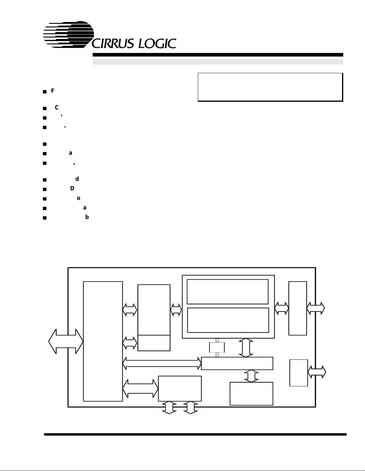
DESCRIPTION
The CS4281 is a PCI audio c ontroller with integrated
legacy games support suitable for desktop and notebook PC designs. Wh en c om bi ned with dr iver s oftw ar e
and an AC ’97 codec such as the CS4297A, this device
provides a complete high quality audio solution. Legacy
compatibility is achieved via PC-PCI, DDMA, and CrystalClear Legacy Support. The product includes an
integrated FM synthesizer and Plug-and-Play interface.
In addition, the CS4281 offers hardware volume control
and power management features. WDM drivers provide
support for Windows 98
used with the CS4297 A, the CS428 1 is fully compliant
with Microsoft’s PC ’98 and PC ‘99 audio requirements.
In the 100-pin MQFP package, the CS4281 is pin-compatible with the CS4614 and CS4280-CM.
ORDERING INFORMATION
CS4281-CM 100-pin MQFP 14x20x2.72mm
CS4281-CQ 100-pin TQFP 14x14x1.4mm
®
and Windows NT®. When
Mixer SRC
DMA
Engine
Controller
Serial AC Link
PCI
PCI Bus
Interface
Interrupt
Control
FM
I/O Register Array
MIDI &
Joystick
Support
PLL &
Clock
GPIO
Control
CIRRUS LOGIC PRODUCT DATA SHEET
DS308PP4 APR ‘99
Copyright Cirrus Logic, Inc. 1999
(All Rights Reserved)

CrystalClear™ PCI Audio Interface
TABLE OF CONTENTS
CHARACTERISTICS/SPECIFICATIONS- - - - - - - - - - - - - - - - - - - - - - - - - - - - - - - - - - 3
Absolute Maximum Ratings - - - - - - - - - - - - - - - - - - - - - - - - - - - - - - - - - - - - - - - - 3
Recommended Operating Conditions - - - - - - - - - - - - - - - - - - - - - - - - - - - - - - - - - 3
AC Characteristics (PCI Signal P ins only) - - - - - - - - - - - - - - - - - - - - - - - - - - - - - - 4
DC Characteristics - - - - - - - - - - - - - - - - - - - - - - - - - - - - - - - - - - - - - - - - - - - - - - 5
PCI Interface Pins- - - - - - - - - - - - - - - - - - - - - - - - - - - - - - - - - - - - - - - - - - - - - - - 6
AC-Link Serial Interface- - - - - - - - - - - - - - - - - - - - - - - - - - - - - - - - - - - - - - - - - - - 7
EEPROM Timing Characteristics - - - - - - - - - - - - - - - - - - - - - - - - - - - - - - - - - - - - 8
OVERVIEW- - - - - - - - - - - - - - - - - - - - - - - - - - - - - - - - - - - - - - - - - - - - - - - - - - - - - - - 9
Legacy Support - - - - - - - - - - - - - - - - - - - - - - - - - - - - - - - - - - - - - - - - - - - - - - - - 9
SYSTEM ARCHITECTURES - - - - - - - - - - - - - - - - - - - - - - - - - - - - - - - - - - - - - - - - - - 9
HOST INTERFACE - - - - - - - - - - - - - - - - - - - - - - - - - - - - - - - - - - - - - - - - - - - - - - - - 11
PCI Bus Transactions - - - - - - - - - - - - - - - - - - - - - - - - - - - - - - - - - - - - - - - - - - - 12
Configuration Space - - - - - - - - - - - - - - - - - - - - - - - - - - - - - - - - - - - - - - - - - - - - 12
Subsystem Vendor ID Fields- - - - - - - - - - - - - - - - - - - - - - - - - - - - - - - - - - - 12
Cirrus-Specific Configuration Registers - - - - - - - - - - - - - - - - - - - - - - - - - - - 15
Interrupt Signal- - - - - - - - - - - - - - - - - - - - - - - - - - - - - - - - - - - - - - - - - - - - - - - - 20
AC ’97 LINK - - - - - - - - - - - - - - - - - - - - - - - - - - - - - - - - - - - - - - - - - - - - - - - - - - - - - 20
MIDI PORT - - - - - - - - - - - - - - - - - - - - - - - - - - - - - - - - - - - - - - - - - - - - - - - - - - - - - - 22
JOYSTICK PORT - - - - - - - - - - - - - - - - - - - - - - - - - - - - - - - - - - - - - - - - - - - - - - - - - 22
EEPROM INTERFACE - - - - - - - - - - - - - - - - - - - - - - - - - - - - - - - - - - - - - - - - - - - - - 23
GENERAL PURPOSE I/O PINS - - - - - - - - - - - - - - - - - - - - - - - - - - - - - - - - - - - - - - - 23
PIN DESCRIPTION - - - - - - - - - - - - - - - - - - - - - - - - - - - - - - - - - - - - - - - - - - - - - - - - 24
PCI Interface - - - - - - - - - - - - - - - - - - - - - - - - - - - - - - - - - - - - - - - - - - - - - - - - - 26
External Interface Pins - - - - - - - - - - - - - - - - - - - - - - - - - - - - - - - - - - - - - - - - - - 27
Clock / Miscellaneous - - - - - - - - - - - - - - - - - - - - - - - - - - - - - - - - - - - - - - - - - - - 28
Serial Codec Interface- - - - - - - - - - - - - - - - - - - - - - - - - - - - - - - - - - - - - - - - - - - 29
PACKAGE OUTLINE- - - - - - - - - - - - - - - - - - - - - - - - - - - - - - - - - - - - - - - - - - - - - - - 30
APPENDIX A. MIGRATION FROM A CS4280 DESIGN TO A CS4281 DESIGN- - - - - 32
CS4281
Contacting Cirrus Logic Support
For a complete listing of Direct Sales, Distributor, and Sales Representative contacts, visit the Cirrus Logic web site at:
http://www.cirrus.com/corporate/contacts/
Preliminary product info rmation describes products which are in production, b ut for which full character izat i on da t a i s not yet available. Advance product information describes products which are in development and subject to development changes. Cirrus Logic, Inc. has made best efforts to ensure that the information
contained in this document is accurate and reliable. However, the information is subject to change without notice and is provided “AS IS” without warranty of any
kind (express o r i mplie d). No re spon sibilit y is as sume d b y Cirru s Logic, Inc. for the use of this information, nor for infringements of patents or other rights of third
parties. This document is the property of Cirrus Logic, Inc. and implies no license under patents, copyrights, trademarks, or trade secrets. No part of this publication may be copied, reproduced, stored in a retrieval system, or transmitted, in any form or by any means (electronic, mechanical, photographic, or otherwise)
without the prior wri tten consent of Ci rrus Lo gic, Inc. Items fr om any Cir rus Logi c websit e or disk may be p rinte d for use by t he user . However , no part of the
printout or electronic files may be copied, reproduced, stored in a retrieval system, or transmitted, in any form or by any means (electronic, mechanical, photographic, or otherwise) wi thout the prior wri tt en consent of Cirrus Log ic, Inc.Furthermore, no part of this publi cati on may be used as a basis for manufacture or
sale of any items without the prior written consent of Cirrus Logic, Inc. The names of products of Cirrus Logic, Inc. or other vendors and suppliers appearing in
this document may be trademarks or service marks of their respect ive owner s which may be registered in some jurisdi ctions. A li st of Ci rru s Logic, Inc. trademarks and service marks can be found at http://www.cirrus.com.
CrystalClear and CCLS are trademarks of Cirrus Logic, Inc.
Windows, Windows 95, Windows 98, and Windows NT are registered trademarks of Microsoft Corporation.
Intel is a registered trademark of Intel Corporation.
Sound Blaster and Sound Blaster Pro are trademarks of Creative Technology, Ltd.
All other names are trademarks, registered trademarks, or service marks of their respective companies.
CIRRUS LOGIC PRODUCT DATA SHEET
2 DS308PP4
CS4281
CrystalClear™ PCI Audio Interface
CHARACTERISTICS/SPECIFICATIONS
ABSOLUTE MAXIMUM RATINGS
(PCIGND = CGND = CRYGND = 0 V, all voltages with respect to 0 V)
Parameter Symbol Min Typ Max Unit
Power Supplies PCIVDD
VAUX
CVDD
CRYVDD
VDD5REF
Total Power Dissipation (Note 1) - - 1.0 W
Input Current per Pin, DC (Except supply pins) - - ±10 mA
Output current per pin, DC - - ±50 mA
Digital Input voltage (Note 2) -0.3 - Vdd+
Ambient temperature (power applied) (Note 3) -55 - 125 °C
Storage temperature -65 - 150 °C
-
-
-
-
-
-
-
-
-
-
4.6
4.6
4.6
4.6
5.5
0.3
V
V
V
V
V
V
Notes: 1. Includes all power generated by AC and/or DC output loading.
2. The power supply pins are at recommended maximum values.
3. At ambient temperatures above 70° C, total power dissipation must be limited to less than 0.4 Watts.
WARNING: Operation beyond these limits may result in permanent damage to the device.
Normal operation is not guaranteed at these extremes.
RECOMMENDED OPERATING CONDITIONS
(PCIGND = CGND = CRYGND = 0 V, all voltages with respect to 0 V)
Parameter Symbol Min Typ Max Unit
Power Supplies PCIVDD
VAUX
CVDD
CRYVDD
VDD5REF
Operating Ambient Temperature T
Specifications are subject to change without notice.
A
3
3.135
3
3
4.75
02570°C
3.3
3.3
3.3
3.3
5
3.6
3.465
3.6
3.6
5.25
V
V
V
V
V
CIRRUS LOGIC PRODUCT DATA SHEET
DS308PP4 3
CS4281
CrystalClear™ PCI Audio Interface
AC CHARACTERISTICS (PCI SIGNAL PINS ONLY)
(TA = 70° C; PCIVDD = CVDD = VAUX = CRYVDD = 3.3 V; VDD5REF = 5 V; PCIGND = CGND = CRYGND = 0 V;
Logic 0 = 0 V, Logic 1 = 3.3 V; Reference levels = 1.4 V; unless otherwise noted; (Note 4))
Parameter Symbol Min Max Unit
Switching Current High (Note 5)
0 < Vout ≤ 1.4
1.4 < Vout < 2.4
3.1 < Vout < 3.3
Switching Current Low (Note 5)
Vout ≥ 2.2
2.2 > Vout > 0.55
0.71 > Vout > 0
Low Clamp Current -5 < Vin ≤ -1 I
Output rise slew rate 0.4 V - 2.4 V load (Note 6) slew
Output fall slew rate 2.4 V - 0.4 V load (Note 6) slew
I
I
OH
OL
CL
-44
Vout 1.4–
44–
-------------------------+
0.024
-
95
Vout/0.023
-
Vin 1+
25–
------------------+
r
f
15V/ns
15V/ns
0.015
-
-
(Note 7)
-
-
(Note 8)
-mA
mA
mA
mA
mA
Notes: 4. Specifications guaranteed by characterization and not production testing.
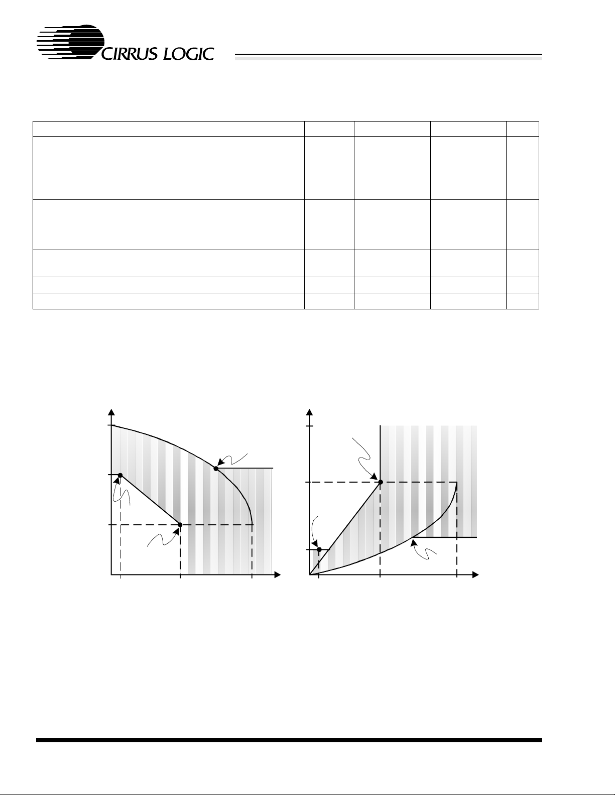
5. Refer to V/I curves in Figure 1. Specification does not apply to PCICLK and RST# signals. Switching
Current High specification does not apply to PME#, CLKRUN#, and INTA# which are open drain outputs.
6. Cumulative edge rate across specified range. Rise slew rates do not apply to open drain outputs.
7. Use Equation A in Figure below.
8. Use Equation B in Figure below.
Pull Down
95
Current (mA)
Vcc
2.4
Voltage
1.4
DC
drive point
AC
drive point
-2
Pull Up
-44
Current (mA)
test
point
-176
Vcc
2.2
Voltage
0.55
AC drive
point
DC drive
point
3, 6
Equation B:Equation A:
test
point
380
IOH = 11.9 × (Vout - 5.25) × (Vout + 2.45)
for 3.3 V > Vout > 3.1 V
IOL = 78.5 × Vout × (4.4 - Vout)
for 0 V < Vout < 0.71 V
Figure 1. AC Characteristics
CIRRUS LOGIC PRODUCT DATA SHEET
4 DS308PP4
CS4281
CrystalClear™ PCI Audio Interface
DC CHARACTERISTICS (T
= 70° C; PCIVDD = VAUX = CVDD = CRYVDD = 3.3 V; VDD5REF = 5 V;
A
PCIGND = CGND = CRYGND = 0 V; all voltages with respect to 0 V unless otherwise noted)
Parameter Symbol Min Typ Max Unit
PCI Interface Signal Pins
High level input voltage V
Low level input voltage V
High level output voltage Iout = -2 mA V
Low level output voltage Iout = 3 mA, 6 mA (Note 9) V
High level leakage current Vin = 2.7 V (Note 10) I
Low level leakage current Vin = 0.5 V I
PME# power off input leakage Vin = 5.25 V (Note 11) I
IH
IL
OH
OL
IH
IL
OFF
2-5.75V
-0.5 - 0.8 V
2.4 - - V
--0.55V
--70µA
---70µA
--1µA
Non-PCI Interface Signal Pins (Note 12)
High level output voltage Iout = -5 mA (Note 13) V
Low level output voltage Iout = 5 mA V
High level input voltage (Note 14) V
Low level input voltage (Note 14) V
High level leakage current Vin = 3.6 V (Note 14) I
Low level leakage current Vin = 0 (Note 14) I
oh
ol
ih
ih
il
0.9×Vdd - V
-0.1
0.65×Vdd Vdd+0.3 V
il
-0.3 0.35×Vdd V
-10µA
--10µA
×
Vdd V
Parameter Min Typ Max Unit
Power Supply Pins (Outputs Unloaded)
Power Supply Current: VDD5REF
VAUX
PCIVDD/CVDD/CRYVDD Total (Note 4)
-
-
-
0.6
TBD
TBD
-
20
TBD
mA
mA
mA
Low Power Mode Supply Current - TBD - mA
Notes: 9. The following signals are tested to 6 mA: FRAME#, TRDY#, IRDY#, DEVSEL#, STOP#, PERR#, and
INTA#. All other PCI interface signals are tested to 3 mA.
10. Input leakage currents include hi-Z output leakage for all bi-directional buffers with three-state outputs.
11. Maximum allowable leakage into the PME# open-drain pin when power is removed from VAUX.
Assumes no event occurred to drive PME# (idle state).
12. For AC-Link and VOLUP/DN pins, Vdd is VAUX. For all others Vdd is the core supply.
13. For open drain pins, high level output voltage is dependent on external pull-up used and number of
attached gates.
14. All inputs that do not include internal pull-ups or pull-downs, must be externally driven for proper
operation. If an input is not driven, it should be tied to power or ground, depending on the particular
function. If an I/O pin is not driven and programmed as an input, it should be tied to power or ground
through its own resistor.
CIRRUS LOGIC PRODUCT DATA SHEET
DS308PP4 5
CS4281
CrystalClear™ PCI Audio Interface
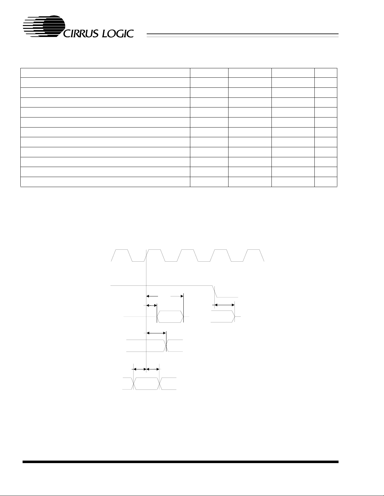
PCI INTERFACE PINS (T
= 0 to 70° C; PCIVDD = CVDD = VAUX = CRYVDD = 3.3 V; VDD5REF =
A
5 V; PCIGND = CGND = CRYGND = 0 V; Logic 0 = 0 V, Logic 1 = 3.3 V; Timing reference levels = 1.4 V)
Parameter Symbol Min Max Unit
PCICLK cycle time t
PCICLK high time t
PCICLK low time t
PCICLK to signal valid delay - bused signals t
PCICLK to signal valid delay - point to point t
val(p+p)
Float to active delay (Note 15) t
Active to Float delay (Note 15) t
Input Set up Time to PCICLK - bused signals t
Input Set up Time to PCICLK - point to point t
su(p+p)
Input hold time for PCICLK t
Reset active to output float delay (Notes 15, 16, 17) t
cyc
high
low
val
on
off
su
h
rst-off
30 - ns
11 - ns
11 - ns
211ns
212ns
2-ns
-28ns
7-ns
10, 12 - ns
0-ns
-30ns
Notes: 15. For Active/Float measurements, the Hi-Z or “off” state is when the total current delivered is less than or
equal to the leakage current. Specification is guaranteed by design, not production tested.
16. RST# is asserted and de-asserted asynchronously with respect to PCICLK.
17. All PCI output drivers are asynchronously floated when RST# is active. Note ASDOUT and ASYNC are
not affected by RST#.
PCICLK
RST#
OUTPUTS
Hi-Z
OUTPUTS
Valid
INPUTS
t
off
t
on
t
val
t
su
Valid
Input
t
h
t
rst-off
Figure 2. PCI Timing Measurement Conditions
CIRRUS LOGIC PRODUCT DATA SHEET
6 DS308PP4
CS4281
CrystalClear™ PCI Audio Interface
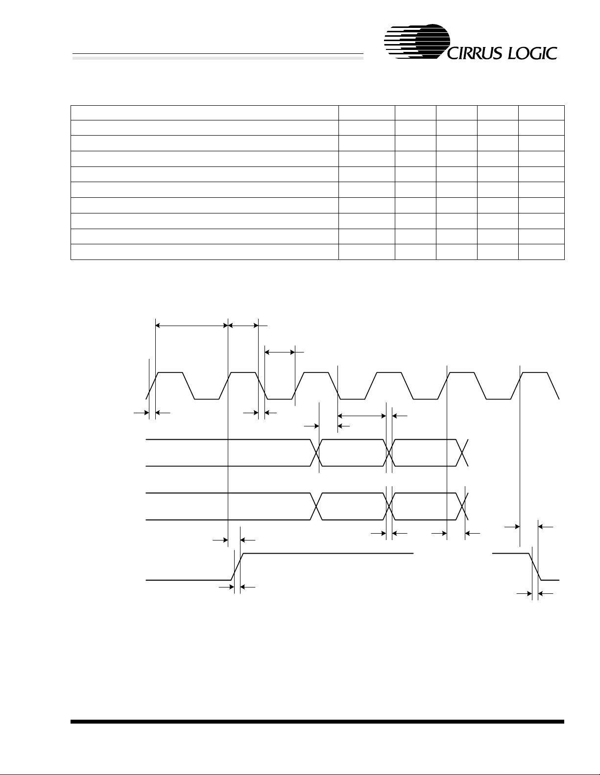
AC-LINK SERIAL INTERFACE (T
= 0 to 70° C; PCIVDD = CVDD = VAUX = CRYVDD = 3.3 V;
A
VDD5REF = 5 V; PCIGND = CGND = CRYGND = 0 V; Logic 0 = V
Parameter Symbol Min Typ Max Unit
ABITCLK input cycle time t
clk_period
ABITCLK input high time t
ABITCLK input low time t
ABITCLK input rise/fall time t
ASDIN/ASDIN2 valid to ABITCLK falling t
ASDIN/ASDIN2 hold after ABITCLK falling t
ASDIN/ASDIN2 input rise/fall time t
ABITCLK rising to ASDOUT/ASYNC valid, C
ASYNC/ASDOUT rise/fall time, C
t
clk_period
= 55 pF t
L
= 55 pF t
L
t
clk_high
t
clk_low
, Logic 1 = Voh,Vih; unless otherwise noted)
ol,Vil
81.4 - ns
clk_high
clk_low
rfclk
setup
hold
rfin
co
rfout
36 40.7 45 ns
36 40.7 45 ns
2-6ns
10 - - ns
10 - - ns
2-6ns
2 - 15 ns
2-6ns
ABITCLK
ASDIN/ASDIN2
ASDOUT
ASYNC
t
rfclk
t
t
setup
hold
t
rfclk
t
co
t
rfout
Figure 3. AC ’97 Configuration Timing Diagram
t
t
rfin
rfout
t
co
t
co
t
rfout
CIRRUS LOGIC PRODUCT DATA SHEET
DS308PP4 7
CS4281
CrystalClear™ PCI Audio Interface
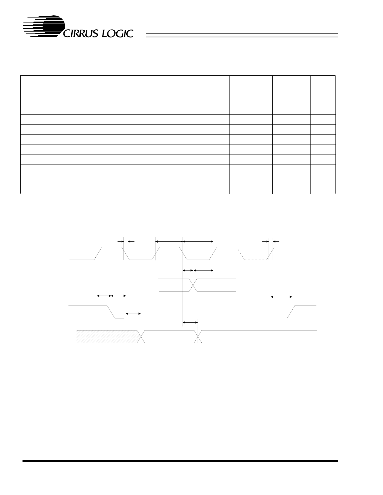
EEPROM TIMING CHARACTERISTICS Note 4. (T
= 0 to 70 °C, PCIVDD = CVDD = VAUX =
A
CRYVDD = 3.3 V; VDD5REF = 5 V; VDD5REF = 5 V; PCIGND = CGND = CRYGND = 0 V; Logic 0 = 0 V,
Logic 1 = 3.3 V; Timing reference levels = 1.4 V; PCI clock frequency = 33 MHz; unless otherwise noted)
Parameter S ymbol Min Ma x Units
EECLK Low to EEDAT Data Out Valid t
Start Condition Hold Time t
EECLK Low t
EECLK High t
Start Condition Setup Time (for a Repeated Start Condition) t
EEDAT In Hold Time t
EEDAT In Setup Time t
HD:STA
LEECLK
HEECLK
SU:STA
HD:DAT
SU:DAT
EEDAT/EECLK Rise Time (Note 18) t
EEDAT/EECLK Fall Time t
Stop Condition Setup Time t
SU:STO
EEDAT Out Hold Time t
AA
R
F
DH
07.0µs
5.0 10 10 -
5.0 -
µ
µ
µ
µ
0-µs
250 - ns
-1µs
- 300 ns
5.0 -
µ
0-µs
s
s
s
s
s
Notes: 18. Rise time on EEDAT is determined by the capacitance on the EEDAT line with all connected gates and
the required external pull-up resistor.
EECLK
EEDAT (IN)
EEDAT (OUT)
EEDAT (OUT)
t
SU:STA
t
LEECLK
t
DH
t
HD:STA
t
AA
t
t
F
HEECLK
t
HD:DAT
Figure 4. EEPROM Timing
t
SU:DAT
t
R
t
SU:STO
CIRRUS LOGIC PRODUCT DATA SHEET
8 DS308PP4

CS4281
CrystalClear™ PCI Audio Interface
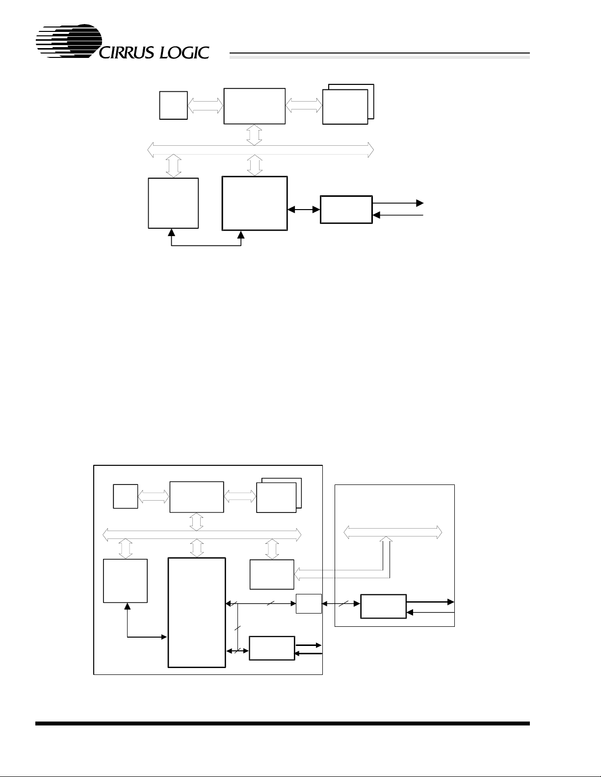
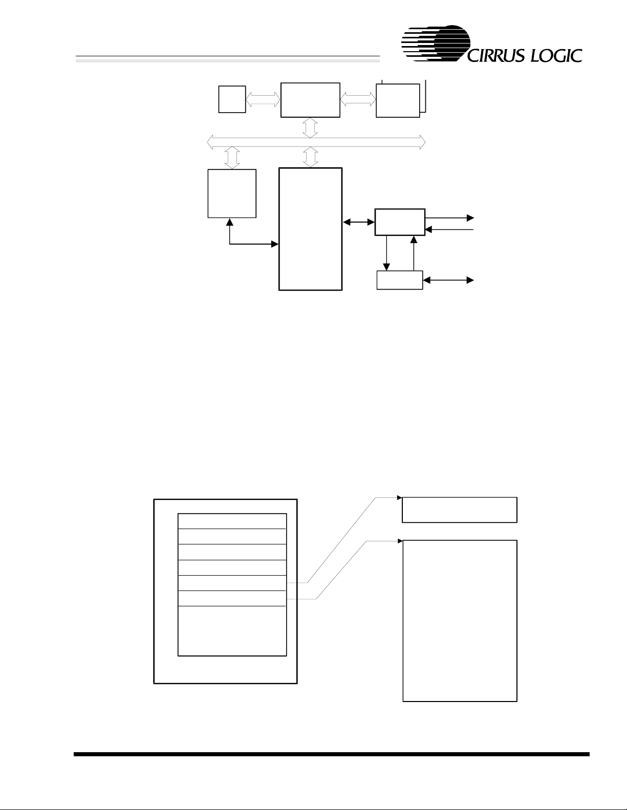
OVERVIEW
The CS4281 provides a low-cost PCI audio solution with Legacy Game com patibilit y for the P C environment. The CS4281 is compatible with the CS4614 and CS4280-CM. The CS4281 is divided into several
functional blocks.
• PCI Interface
• Sound System Interface
• FM Synthesis
• Peripheral Devices (MIDI & Gameport)
The PCI Interface is the physical connection to the bus. It is subdivided into several smaller functional
groups such as: PCI configuration and interface, DMA controller, interrupt control, and chip control. The
PCI interface serves as a Master/Target PCI device and its two-base address registers provide access to the
chip operation registers and internal memory blocks. The Sound System Interface provides all the registers
and controls to operate the entire sou nd system. The FM Synthes is provides full compa tibility with market
standard FM-based music synthesis used in DOS games and educational software. The CS4281’s flexibility is further enhanced by the inclusion of peripheral devices such as Hardware Volume Control, Clock
Generation, General Purpose I/O (GPIO), MIDI UART Port, Game (Joystick) Port, and the AC Link.
The DMA Engine provides dedicated hardware to manage transfer of up to 4 concurrent audio/data streams
to and from host memory buffers. Four Bus Mastering DMA controllers support simultaneous capture,
play, modem transmit, and modem receive.
The CS4281 supports a variety of audio I/O configurations including a single CS4297A CrystalClear
AC ’97 Codec or dual CS4297A codecs where the second codec is used as a portable’s docking station
solution. The combination of a CS4281 with a CS4298 AMC ‘97 codec, provides a cost-effective, superior
quality, two-chip audio/modem solution.
Legacy Support
Legacy games are supported by CrystalClear Legacy Support CCLS™, DDMA, or by the PC/PCI interface. In both motherboard and add-in card designs, CCLS and DDMA provide support for legacy games
by providing a hardware interface that supports a Sound Blaster Pro™ compatible interface, as well as support for FM, and joystick interfaces. These ha rdware in terface s provide PC I-only gam es compa tibi lity for
real-mode DOS and Windows DOS box support.
For motherboard designs, PC/PCI is used by connecting the PCGNT# and PCREQ# pins to the appropriate
pins on the south bridge motherboard chip. The PC/PCI interface is compliant with Intel’s PC/PCI spec.
(version 1.2).
SYSTEM ARCHITECTURES
A typical system diagram depicting connection of the CS4281 to the CrystalClear CS4297A AC ’97 Codec
is given in Figure 5. All analog audio inputs and outputs are connected to the CS4297A. Audio data is
passed between the CS4297A and the CS4281 over the serial AC-Link. The CS4281 provides a hardware
interface for connection of a joystick and MIDI devices.
Figure 6 depicts the CS4281 using both AC ‘97 codec interfaces in a portable design. The primary AC ‘97
interface is connected to a CS4297A used for all audio I/O inside and connected to the portable. The second
AC ‘97 interface is sent across to the docking station which contains a second CS4297A. The second codec
CIRRUS LOGIC PRODUCT DATA SHEET
DS308PP4 9
CS4281
CrystalClear™ PCI Audio Interface
CPU
North
Bridge
Host
Memory
PCI Bus
South
Bridge
CS4281
CS4297A
Audio Out
Audio In
PC/PCI (if used)
Figure 5. AC ‘97 Codec Interface
is activated when the portable is in the docking station. Software can disable the audio I/O paths on the
portable that are superseded by docking station I/O and enable the paths needed in the docking station.
Note that both interfaces are needed in systems where the CD-ROM analog input is in the portable and the
Line In/Out jacks on the docking stations are used. Using the AC ‘97 digital link across the dock maintains
the absolute highest audio quality along with a standard well-defined non-proprietary interface that will
last through many system generations.
Figure 7 depicts the CS4281 using an AC ‘97 codec in an audio/modem design. The primary AC ‘97 interface is connected to a CS4298 and is used for audio/modem I/O such as Mic In, Line In, Line Out and
the Analog Front End (AFE) for Modem features. The CS4298 analog interface is connected to the DAA
via the EGPIO pins. The EGPIO supports the PCI Power Management Event system wake-up feature allowing a powerdown system to be powered up by an incoming call on the modem.
PORTABLE
CPU
South
Bridge
North
Bridge
PCI Bus
CS4281
PCI Audio Interface
Secondary
Serial Data
(ASDIN2)
PC/PCI
(if used)
Primary
AC-Link
Host
Memory
Bridge
1
In
4
5
5
CS4297A
Buffer
Audio
Out
Audio
In
DOCKING STAT ION
Secondary PCI Bus
5
CS4297A
Audio Out
Audio In
Figure 6. Portable Docking Station Scenario
CIRRUS LOGIC PRODUCT DATA SHEET
10 DS308PP4
CS4281
CrystalClear™ PCI Audio Interface
CPU
South
Bridge
North
Bridge
PCI Bus
CS4281
PCI Audio Interface
AC-Link
PC/PCI
(if used)
Host
Memory
CS4298
DAA
Audio Out
Audio In
Telephone
Line
Figure 7. Modem Scenario
HOST INTERFACE
The CS4281 host interface is comprised of two separate interface blocks which are memory mapped into
host address space. The interface blocks can be located anywhere in the host 32-bit physical address space.
The interface block locations are defined by the addresses programmed into the two Base Address Regis-
ters in the PCI Configuration Space. These base addresses are normally set up by the system’s Plug and
Play BIOS. The first interface block (Base Address 0) contains the general purpose configuration, control,
and status registers for the device. The second interface block (Base Address 1) maps the FIFO RAMs into
host memory space. The relationship between the Base Address Registers in the CS4281 PCI Configuration Space and the host memory map is depicted in Figure 8. The bus mastering PCI bus interface complies
with the PCI Local Bus Specification (version 2.1).
Device PCI Config. Space
00h
Device ID / Vendor ID
04h
08h
0Ch
10h
14h
Status / Command
Class Code / Revision
Misc. Control
Base Address Register 0
Base Address Register 1
Direct Registers
(Memory Mapped, 4 kByte)
Direct Memory Interface
(Memory Mapped, 6 kByte)4
Figure 8. Host Interface Base Address Registers
CIRRUS LOGIC PRODUCT DATA SHEET
DS308PP4 11

CS4281
CrystalClear™ PCI Audio Interface
PCI Bus Transactions
As a target of a PCI bus transaction, the CS4281 supports the Memory Read (from internal registers or
memory), Memory Write (to internal registers or memory), Configuration Read (from CS4281 configuration registers), Configuration Write (to CS4281 configuration registers), Memory Read Multiple (aliased
to Memory Read), Memory Read Line (aliased to Memory Read), and the Memory Write and Invalidate
(aliased to Memory Write) transfer cycles. The I/O Read, I/O Write, Interrupt Acknowledge, Special Cycles, and Dual Address Cycle transactions are not supported.
As a Bus Master, the CS4281 generates the Memory Read and Memory Write transactions. The Memory
Read, Configuration Read, Configuration Write, Memory Read Line, Memory Write and Invalidate, I/O
Read, I/O Write, Interrupt Acknowledge, Special Cycles, and Dual Address Cycle transactions are not
generated.
The PCI bus transactions supported by the
CS4281 device are summarized in Table 1. Note
that no Target Abort conditions are signalled by
the device. Byte, word, and doubleword transfers
are supported for Configuration Space accesses.
Only doubleword transfers are supported for Register and Memory area accesses. Bursting is not
supported for host-initiated transfers to/from the
CS4281 internal register space, RAM memory
space, or PCI configuration space (disconnect after first phase of transaction is completed).
Configuration Space
The content and format of the PCI Configuration
Space is given in Table 2. The registers from 00 to
44h are standard PCI configuration registers. The registers from E0h to FFh are Cirrus-Logic specific and
are read-only by default. For protection from inadvertent writes, the Configuration Space registers from
E4h to FFh are read-only unless the CWPR register at E0h is loaded with 4281h. Once CWPR contains
4281h, the registers are writable.
Initiator Target Type PCI Dir
Host Registers (BA0) Mem Write In
Host Registers (BA0) Mem Read Out
Host Memories (BA1) Mem Write In
Host Memories (BA1) Mem Read Out
Host Config Space 1 Config Write In
Host Config Space 1 Config Read Out
DMA Host System Mem Write Out
DMA Host System Mem Read In
Table 1. PCI Interface Transaction Summary
Subsystem Vendor ID Fields
The Subsystem ID and Subsystem Vendor ID fields can be loaded in two ways. Typically add-in cards use
an external EEPROM where the CS4281 loads the data from EEPROM on power-up. For mother-board
systems the BIOS typically loads the Configuration Space at offset FCh (see Table 2). Once these values
are loaded they will appear in the Configuration Space offset 2Ch. The Subsystem ID and Subsystem Vendor ID fields in the PCI Configuration Space default to value 0000h. The CWPR register a t E0h must be
loaded with 4281h on order to write the Subsystem IDs at FCh.
CIRRUS LOGIC PRODUCT DATA SHEET
12 DS308PP4

CS4281
CrystalClear™ PCI Audio Interface
Byte 3 Byte 2 Byte 1 Byte 0 Offset
Device ID: R/O, 6005h for CS4281 Vendor ID: R/O, 1013h 00h
Status Register, bits 15-0:
Bit 15: Detected Parity Error: Error Bit
Bit 14: Signalled SERR: R/O: 0
Bit 13: Received Master Abort: Error Bit
Bit 12: Received Target Abort: Error Bit
Bit 11: Signalled Target Abort: R/O 0
Bit 10-9: DEVSEL Timing: R/O, 01b (medium)
Bit 8: Data Parity Error Detected: Error Bit
Bit 7: Fast Back to Back Capable: R/O 0
Bit 6: User Definable Features: R/O 0
Bit 5: 66MHz Bus: R/O 0
Bit 4: New Capabilities: R/O 1
Bit 3-0: Reserved R/O 000
Reset Status State: 0210h
Write of 1 to any error bit position clears it.
Class Code: R/O 040100h
Class 04h (multimedia device), Sub-class 01h (audio), Interface 00h
Header Type:
BIST: R/O 0
Base Address Registe r 0
Device Control Register space, memory mapped. 4kByte size
Bit 31-12: R/W, default 0. Compare address for register space accesses
Bit 11 - 4: R/O 0, specifies 4kByte size
Bit 3: R/O 0, Not Prefetchable (Cacheable)
Bit 2-1: R/O 00, Location Type - Anywhere in 32 bit address space
Bit 0: R/O 0, Memory space indicator
Base Address Registe r 1
Device Memory Array mapped into host system memory space, 64kByte size
Bit 31-16: R/W, default 0. Compare address for memory array accesses
Bit 15-4: R/O 0, specifies 64kByte size
Bit 3: R/O 0, Not Prefetchable (Cacheable)
Bit 2-1: R/O 00, Location Type - Anywhere in 32 bit address space
Bit 0: R/O 0, Memory space indicator
Base Address Register 2: R/O 0000000 0h, Unus ed 18h
Base Address Register 3: R/O 0000000 0h, Unus ed 1Ch
Base Address Register 4: R/O 0000000 0h, Unus ed 20h
Base Address Register 5: R/O 0000000 0h, Unus ed 24h
Cardbus CIS Pointer: R/O 00000000h, Unused 28h
Bit 7: R/O 0
Bit 6-0: R/O 0 (type 0)
Command Register, bits 15-0:
Bit 15-10: Reserved, R/O 0
Bit 9: Fast B2B Enable: R/O 0
Bit 8: SERR Enable: R/O, 0
Bit 7: Wait Control: R/O 0
Bit 6: Parity Error Response: R/W, default 0
Bit 5: VGA Palette Snoop: R/O 0
Bit 4: MWI Enable: R/O 0
Bit 3: Special Cycles: R/O 0
Bit 2: Bus Master Enable: R/W, default 0
Bit 1: Memory Space Enable: R/W, default 0
Bit 0: IO Space Enable: R/O 0
Revision ID: R/O 01h 08h
Latency Timer:
Bit 7-3: R/W,default 0
Bit 2-0: R/O 0
Cache Line Size:
R/O 0
0Ch
04h
10h
14h
Table 2. PCI Configuration Space
CIRRUS LOGIC PRODUCT DATA SHEET
DS308PP4 13

CS4281
CrystalClear™ PCI Audio Interface
Byte 3 Byte 2 Byte 1 Byte 0 Offset
Subsystem ID
R/O 0000h default, see
Expansion ROM Base Address: R/O 00000000h, Unused 30h
Reserved: R/O 000000h Cap_Ptr: R/O, 40h 34h
Reserved: R/O 00000000h 38h
Max_Lat: R/O 18h
24 × 0.25 µS = 6 µS
PMC
Bit 15: PME# from D3cold: R/O 0 default
Bit 14: PME# from D3hot: R/O 1
Bit 13: PME# from D2: R/O 1
Bit 12: PME# from D1: R/O 1
Bit 11: PME# from D0: R/O 1
Bit 10: D2 support: R/O 1
Bit 9: D1 support: R/O 1
Bit 8-6: Vaux Power: R/O 000 default
Bit 5: Device Specific Init: R/O 1
Bit 4: Auxiliary Power: R/O 0 default
Bit 3: PME# clock: R/O 0
Bit 2-0: V ersion: R/O 001
Data: R/O 0 PMCSR_BSE: R/O 0
Serial Port Power Management & Control (SPMC): R/W* 00000000h ECh
BIOS Flags: R/W* 00h ISA IRQC: R/W* 00h ISA IRQB: R/W* 00h ISA IRQA: R/W* 00h F4h
Subsystem ID:
R/W* 0000h default
* Write capability controlled by CWPR setting.
†
Power-up values could be loaded from external EEPROM.
Subsystem ID
Min_Gnt: R/O 04h
4 × 0.25 µS = 1 µS
Configuration Write Protect (CWPR): R/W 00000000h E0h
GPIO Pin Interface (GPIOR): R/W* 00000000h E8h
Configuration Load Register (CFLR): R/W* 00000000h default
†
, see Subsystem ID section
section
Reserved E4h
Reserved F8h
Subsystem Vendor ID
R/O 0000h default, see
Interrupt Pin:
R/O 01h, INTA used
Next Item Pointer:
R/O 00h
PMCSR
Bit 15: PME# status: R/W 0
Bit 14-13: Data scale: R/O 00
Bit 12-9: Data select: R/O 0000
Bit 8: PME_En: R/W 0
Bit 7-2: Reserved: R/O 000000
Bit 1-0: Power state: R/W 00
Subsystem Vendor ID:
R/W* 0000h default†, see Subsystem ID section
Subsystem ID
Interrupt Line:
R/W, default 0
Capability ID:
R/O 01h
†
section
2Ch
3Ch
40h
44h
F0h
FCh
Table 2. PCI Configuration Space
CIRRUS LOGIC PRODUCT DATA SHEET
14 DS308PP4
(cont.)

CS4281
CrystalClear™ PCI Audio Interface
Cirrus-Specific Configuration Registers
Configuration Space locations E0h through FFh are Cirrus-specific registers and are only listed in the PCI
specification as vendor-defined. E0h is the Configuration Write Protect register (CWPR) and blocks registers E4h through FFh from being written (they are read-only), when the CWPR register is anything but
4281h. When CWPR is programmed for 4281h, registers E4h through FFh are writable. This section will
describe the Cirrus-specific Configuration registers with the exception of the Subsystem ID register at FCh
which was described in the last section.
The Cirrus-specific registers provide the BIOS with access to general setup and configuration options of
the CS4281. Placing these registers in the Configuration Space lets the BIOS configure the CS4281 before
any operating system has assigned memory base addresses. Some general-purpose bits are also available
to allow the BOIS to communicate with the CS4281 driver software. Cirrus Logic must be contacted before
using any of these general-purpose bits when using Cirrus-supplied software drivers.
General Purpose I/O Register (GPIOR)
31 30 29 28 27 26 25 24 23 22 21 20 19 18 17 16
GP3W GP3ST GP3PT GP3OE GP1W GP1ST GP1PT GP1OE VUPW VUPST VUPPO VUPLT VDNW VDNST VDNPO VDNLT
1514131211109876543210
GP3D GP1D GPPS GPSS GP3S GP1S VUPS VDNS
Address: PCI CFG: E8h, Read-Write if CWPR configured, otherwise Read-Only
Definition: The General Purpose I/O register provides a host port for accessing extended general-purpose I/O
Bit Descriptions:
VDNS VOLDN input Status: This bit reflects the status of the VOLDN input pin. If configured as sticky
VUPS VOLUP input Status: This bit reflects the status of the VOLUP input pin. If configured as sticky
GP1S ASDIN2/GPIO1 input Status: Assuming this pin is not config ured for ASDIN2, thi s bit reflects
GP3S GPIO3 input Status: This bit reflects the status of the GP IO3 pin itself. If G PIO3 is an o utput,
pins.
(VDNST=1), VDNS reads one when the VOLDN pin goes active (edge sensitive - edge
defined by polarity bit VDNPO), and is cleared by writing a 0 to VDNS.
If configured as leve l sens it iv e ( VDN ST= 0) , thi s bit r efl ects the c urr ent s tate of th e VO L DN pin
qualified by the polarity bit VDNPO.
(VUPST=1), VUPS reads one when the VOLUP pin goes active (edge sensitive - edge defined
by polarity bit VUPPO), and is cleared by writing a 0 to VUPS.
If configured as level sensi tive (VUP ST=0), thi s bit refle cts the curre nt state of the VOL UP pin
qualified by the polarity bit VUPPO.
the status of the ASDIN2/G PIO 1 p in . If AS DIN2 /GPIO 1 is a n o utp ut, this bit refl ec ts the actual
state of the pin. If ASDIN2/GPIO1 is an input:
If configured as sticky (GP1ST=1), this bit reads one when the ASDIN2/GPIO1 pin goes active
(edge sensitive - edge defined by polarity bit GP1PT), and is cleared by writing a 0 to GP1S.
If configured as level sensitive (GP1ST=0), this bit reflects the current state of the
ASDIN2/GPIO1 pin qualified by the polarity bit GP1PT.
See the
this bit reflects the actual state of the pin. If GPIO3 is an input:
If configured as sti cky (GP3ST=1), t his bit reads one when the GPIO3 pin goes active (edg e
sensitive - edge defined by polarity bit GP3PT), and is cleared by writing a 0 to GP3S.
If configured as level s ensitive (GP3S T=0), this bit reflects the curren t state of the GPIO3 pin
qualified by the polarity bit GP3PT.
Serial Port Power Management Control
(SPMC) register description of ASDI2E bit.
CIRRUS LOGIC PRODUCT DATA SHEET
DS308PP4 15

CS4281
CrystalClear™ PCI Audio Interface
GPSS GP_INT input Secondary Status. A general purpose input pin on the Secondary Codec
(ASDIN2) caused AC-Lin k slot 12, GP_INT to set. Writing GPSS = 0 clears the locally stored
copy; however, since the interrupt condition occurred in the Secondar y Codec, the condi tion
must be removed through the Secondary Codec GPIO Pin Sticky register, Index 54h.
GPPS GP_INT input Primary Status. A general purpos e inpu t pin on the Primar y Code c ca used A C-
GP1D GPIO1 output data. When ASDIN2/GPIO1 is not ASDIN2 and is configured as an output
GP3D GPIO3 output data. When configured as an output (GP3OE = 1), writes to this bit are
VDNLT Volume Down Load/Type. Function dependent on whether hardware volume is enabled.
VDNPO Volume Down input Polarity.
VDNST Volume Down input Sticky.
VDNW Volume Down Wake. When set, VOLDN can cause a wake-up event (asserts PME#). VDNST
VUPLT Volume Up Load/Type. Function dependent on whether hardware volume is enabled.
VUPPO Volume Up input Polarity.
VUPST Volume Up input Sticky.
VUPW Volume Up Wake-up. When set, VOLUP can cause a wake-up event (asserts PME#). VUPST
GP1OE Outpu t Enable ASDIN2/GPIO1. When this pin is not configured as ASDIN2, setting this bit
Link slot 12, G P_INT to s et. Writing GPPS = 0 clears t he loca lly stored copy; h owever, since
the interrupt condi tion occurr ed in the P rima ry codec, th e con dit ion m ust be rem oved t hroug h
the Primary Codec GPIO Pin Sticky register, Index 54h.
(GP1OE = 1), writes to this bit are presented on the ASDIN2/GPIO1 pin.
presented on the GPIO3 pin. Note that in backward-compatible sockets, this pin is a PCI
power supply pin.
Hardware Volume Control Enabled:
0 - GPIO logic input reflects the pin status directly
1 - GPIO logic input is pulse from Down hardware volume control logic. When a hardware
volume change is generated from VOLDN, a pulse is sent to this GPIO input.
Hardware Volume Control Disabled:
0 - Enable VOLDN pin pullup
1 - Disable VOLDN pin pullup
0 - active low
1 - active high
1 - VOLDN input pin is latched, for edge sensitive inputs, and presented on the VNDS bit. The
VDNS bit is cleared by writing a 0 to VDNS.
0 - VOLDN input pin (after VNDPO) is presented on VDNS bit for level sensitive inputs.
must be set sticky for this bit to be effective.
Hardware Volume Control Enabled:
0 - GPIO logic input reflects the pin status directly
1 - GPIO logic input is pulse from Up hardware volume control logic. When a hardware volume
change is generated from VOLUP, a pulse is sent to this GPIO input.
Hardware Volume Control Disabled:
0 - Enable VOLUP pin pullup
1 - Disable VOLUP pin pullup
0 - active low
1 - active high
1 - VOLUP input pin is latched, for edge sensitive inputs, and presented on the VUPS bit. The
VUPS bit is cleared by writing a 0 to VUPS.
0 - VOLUP input pin (after VUPPO) is presented on VUPS bit for level sensitive inputs.
must be set sticky for this bit to be effective.
enables the output buffer allowing writes to the GP1D bit to be presented on the pin.
0 - Output disabled, pin is configured as an input (reset default)
1 - Output enabled
CIRRUS LOGIC PRODUCT DATA SHEET
16 DS308PP4

CS4281
CrystalClear™ PCI Audio Interface
GP1PT GPIO1 input Polarity/output Type. When ASDIN2/GPIO1 is not configured as ASDIN2:
When ASDIN2/GPIO1 pin is configured as an input (GP1OE = 0), this bit sets the polarity.
0 - active low input
1 - active high input
When ASDIN2/GPIO1 pin is configured as an output (GP1OE = 1), this bit sets the type
0 - CMOS output
1 - open drain output
GP1ST GPIO1 input Sticky. Assumes GP1OE = 0 and pin not configured for ASDIN2.
GP1W GPIO1 Wake. When set, GPIO1 can cause a wake-up event (asserts PME#). GP1ST must be
GP3OE Output Enable GPIO3: Setting this bit enables the output buffer allowing writes to the GP3D bit
GP3PT GPIO3 input Polarity/output Type.
GP3ST GPIO3 input Sticky. Assumes GP3OE = 0.
GP3W GPIO3 Wake. When set, GPIO3 can cause a wake-up event (asserts PME#). GP3ST must be
1 - GPIO1 input pin is latched , for edge se nsitive inp uts, and presented on the GP1S bit. The
GP1S bit is cleared by writing a 0 to GP1S.
0 - GPIO1 input pin (after GP1PT) is presented on GP1S bit for level sensitive inputs.
set sticky for this bit to be effective and the pin must not be configured for ASDIN2.
to be presented on the GPIO3 pin. Note that in backwards-compatible sockets, this pin is a
PCI power supply pin.
0 - Output disabled, pin is configured as an input (reset default)
1 - Output enabled
When the GPIO3 pin is configured as an input (GP3OE = 0), this bit sets the polarity.
0 - active low input
1 - active high input
When the GPIO3 pin is configured as an output (GP3OE = 1), this bit sets the type
0 - CMOS output
1 - open drain output
1 - GPIO3 input pin is latched , for edge se nsitive inp uts, and presented on the GP3S bit. The
GP3S bit is cleared by writing a 0 to GP3S.
0 - GPIO3 input pin (after GP3PT) is presented on GP3S bit for level sensitive inputs.
set sticky for this bit to be effective.
Serial Port Power Management Control (SPMC)
31 30 29 28 27 26 25 24 23 22 21 20 19 18 17 16
1514131211109876543210
GIPPEN GISPEN EESPD ASDI2E res WUP2 WUP1 ASYN RSTN
Address: PCI CFG: ECh, Read-Write if CWPR configured, otherwise Read-Only
Definition: Supports power management of the AC Link and the enable for ASDIN2. This register is unaffected
by the PCI RST# signal.
Bit Descriptions:
RSTN Reset NOT!: This bit controls the ARST# pin. Note the negative sense of the bit, which
ASYN Asynchronous ASYNC Assertion: This bit allows the unclocked assertion of the ASYNC pin for
matches the active l ow out put pi n defi nition . The A RST# p in is a l ogical OR o f RST N with the
PCI reset pin RST#.
0 = ARST# active, AC-Link and Codec reset (reset default)
1 = ARST# inactive, AC-Link and Codec not reset (normal operation).
AC-Link management protocol requirements.
0 = Normal ASYNC generation (reset default)
1 = Force ASYNC high
CIRRUS LOGIC PRODUCT DATA SHEET
DS308PP4 17

CS4281
CrystalClear™ PCI Audio Interface
WUP1 Wakeup for primary input: This bit indicates that a Codec attached to the ASDIN pin signaled a
wake-up event by forcing a low-to-high transition on ASDIN while the AC-Link is down. This bit
remains set until hos t dr i ver sof tware i s sues a wa rm res et o f th e A C-L in k b y se ttin g th e A SY N
bit; specifically, the falling edge of the ASYNC warm reset pulse clears this bit.
0 = No wake-up event signaled by ASDIN
1 = Wake-up event signaled by ASDIN
WUP2 Wakeup for secondary input: This bit indicates that a Codec attached to the ASDIN2 pin
signaled a wake-up event by forci ng a low-to-high tr ansition on ASDIN 2 while the AC -Link is
down. This bit remains set until host driver software issues a warm re set of the AC-Link by
setting the ASYN bit; s pecifically, the falling edge o f the ASYNC war m reset puls e clears this
bit.
0 = No wake-up event signaled ASDIN2
1 = Wake-up event signaled by ASDIN2
GIPPEN G P_INT Primary PME# Enable for primary ASDIN2 Slot 12 data. When set, allows Primary
GISPEN G P_INT Secondar y PME# Enable for secondary ASDIN2 Slot 12 data. When set, a llows the
EESPD EEPROM Serial Po rt Disable. When set, the EEPROM engine is disa bled and does NO T try
ASDI2E ASDIN2 Enable.
Codec’s slot 12 to generate a PME event when GP_INT goes from 0 to a 1.
Secondary Codec to generate a PME event when GP_INT goes from 0 to a 1.
and read the EERPOM on a power-o n reset. The two EEPROM pins are also dis connected
from the EEPROM e ngine. When clear, the EEPROM en gine is en abled and goes ou t on the
EEPROM port and tries to read the EEPROM after a power-on reset.
0 = ASDIN2 function disabled (reset default) (converts to extended GPIO1).
1 = ASDIN2 function enabled (implies a Secondary Codec is attached)
Configuration Load Register (CFLR)
31 30 29 28 27 26 25 24 23 22 21 20 19 18 17 16
CB37 CB36 CB35 CB34 CB33 CB32 CB31 CB30 CB27 CB26 CB25 CB24 CB23 CB22 CB21 CB20
1514131211109876543210
CB17 CB16 CB15 CB14 CB13 CB12 CB11 CB10 CB07 CB06 CB05 CB04 CB03 CB02 CB01 CB00
Address: PCI CFG: F0h, Read-Write if CWPR configured, otherwise Read-Only
Definition: The Configuration Load Register provides a host port for reading of four bytes of device configura-
Bit Descriptions:
CB0[7:0] This bit field returns the first configuration byte.
CB1[7:0] This bit field returns the second configuration byte.
CB2[7:0] This bit field returns the third configuration byte
CB3[7:0] This bit field returns the fourth configuration byte.
tion options from EE PROM. The BIOS can pre- load this register by wr iting to it in configura tion
space. The follow ing bit descripti ons are for driver information on ly as these bits have no direct
hardware affect. When using the Cirrus software drivers, contact Cirrus before using any of these
bits as they may have pre-defined meanings.
CIRRUS LOGIC PRODUCT DATA SHEET
18 DS308PP4

CS4281
CrystalClear™ PCI Audio Interface
ISA Interrupt Select Register (IISR)
31 30 29 28 27 26 25 24 23 22 21 20 19 18 17 16
VAUXS VAC2 VAC1 VAC0 AUXP BCF2 BCF1 B CF0 GTD IRQC3 IRQC2 IRQC1 IRQC0
1514131211109876543210
IRQB3 IRQB2 IRQB1 IRQB0 IRQA3 IRQA2 IRQA1 IRQA0
Address: PCI CFG: F4h, Read-Write if CWPR configured, otherwise Read-Only
Definition: Defines the ISA interrupt associated with a particular pin and relays flags from BIOS to the OS and
host software. This register is unaffected by the PCI RST# signal.
Bit Descriptions:
VAUXS Vaux Support. This bit is reflec ted into the D3
generally set this bit if VAUX is supported.
support bit, PM C.P MD3C. BIOS code w oul d
cold
VAC[2:0] Vaux Current. These bits are re flected in th e PMC .VAC[2:0] bits and must be initialized by the
BIOS to indicate how much current Vaux pulls. Note this is total c urrent and is the combined
CS4281 and any attached Codecs and external logic using Vaux.
000 - 0 mA (self powered/don’t support Vaux)
001 - 55 mA
010 - 100 mA
011 - 160 mA
100 - 220 mA
101 - 270 mA
110 - 320 mA
111 - 375 mA (spec maximum)
AUXP Auxiliary Power. This bit is reflected in the PMC.AUXP bit.
BCF[2:0] BIOS Configuration Flags. These bits have no direct affect on the operation of the CS4281 and
may be used by host software when communicating with the BIOS.
GTD Global Trapping Disab le. When set, d isab les a ll I/O t rapping. When GTD is clear, I/O trapping
is allowed (must be configured through other registers).
IRQA[3:0] IRQA pin interrupt mappin g. A 0 disables (high impedance) th e corresponding ISA interrupt
pin. A non-zero value (prefe rably the actual ISA inter rupt connect ed to the pin) allows the pin
to be enabled through software drivers.
IRQB[3:0] IRQB pin interrupt mappin g. A 0 disables (high impedance) th e corresponding ISA interrupt
pin. A non-zero value (prefe rably the actual ISA inter rupt connect ed to the pin) allows the pin
to be enabled through software drivers.
IRQC[3:0] IRQC pin inter rupt mapping. A 0 disa bles (high impedance) th e corresponding ISA inte rrupt
pin. A non-zero value (prefe rably the actual ISA inter rupt connect ed to the pin) allows the pin
to be enabled through software drivers.
CIRRUS LOGIC PRODUCT DATA SHEET
DS308PP4 19

CS4281
CrystalClear™ PCI Audio Interface
Interrupt Signal
The CS4281 PCI Interface includes an interrupt controller function which receives interrupt requests from
multiple sources within the CS4281 device, and presents a single interrupt line (INTA) to the host system.
Interrupt control registers in the CS4281 provide the host int errupt service routine with the abilit y to identify the source of the interrupt and to clear the interrupt sources.
ISA interrupts are provided for real-mode DOS support. The three ISA interrupt pins are high-impedance
when the CS4281 powers up. The output enables for a particular ISA interrupt are a combination of bits
set by the BIOS and an interrupt enable bit controlled by start-up configuration software.
AC ’97 LINK
The CrystalClear solution includes a CS4281 plus a CS4297A. The CS4281 communicates with the
CS4297A over the AC-Link as specified in the Intel® Audio Codec ‘97 Specification (version 2.1). A
block diagram for the AC ’97 Controller configuration is given in Figure 5. The signal connections between the CS4281 and the AC ’97 Codec are indicated in Figure 9.
CS4281
JACX, JACY, JBCX, JBCY
JAB1, JAB2, JBB1, JBB2
ABITCLK
ASYNC
ASDOUT
ASDIN
ARST#
MIDIIN
MIDIOUT
Figure 9. Single AC ‘97 Codec Connection Diagram
12.288 MHz
48 kHz
24.576 MHz
BIT_CLK
SYNC
SDATA_OUT
SDATA_IN
RESET#
Analog Interface
CS4297A
Joystick/
MIDI Port
CIRRUS LOGIC PRODUCT DATA SHEET
20 DS308PP4

CS4281
CrystalClear™ PCI Audio Interface
The dual codec architecture of AC ‘97, version 2.1, is supported wherein the second codec uses the same
pins from the primary, with the exception of a separate serial data-in line (ASDIN2) illustrated in
Figure 10. The Primary Codec is the timing master for the digital audio link and the CS4281. The ASDOUT output supports data transmission on nine of the output s ample slots (output slots 3 - 11). The ASDIN
and ASDIN2 inputs support receiving of audio sample data on nine of the input sample slots (input slots
3 - 11).
ABITCLK
ASYNC
ASDOUT
ASDIN
ARST#
CS4281
ASDIN2
MIDIIN
MIDIOUT
JACX, JACY, JBCX, JBCY
JAB1, JAB2, JBB1, JBB2
12.288 MHz
48 kHz
BIT_CLK
SYNC
SDATA_OUT
SDATA_IN
RESET#
24.576 MHz
Analog Interface
CS4297/97A
BIT_CLK
SYNC
SDATA_OUT
RESET#
SDATA_IN
Analog Interface
CS4297A
(AC ’97 2.0)
Joystick/
MIDI Port
Figure 10. Dual AC ‘97 Codec Connection Diagram
CIRRUS LOGIC PRODUCT DATA SHEET
DS308PP4 21

CS4281
CrystalClear™ PCI Audio Interface
MIDI PORT
A bi-directional MIDI interface allows connection of external MIDI devices. The MIDI interface includes
a 16-byte FIFO for the MIDI receive path. A MIDI buffer (see Figure 11) is recommended due to some
joystick manufactures grounding the MIDIOUT pin.
CS4281
MIDIOUT
3.3V
39k
39k
MMBT2907ALT1
10k
20k
5.1k
5V
MMBT3904LT1
MIDIOUT
(Buffered)
Joystick
Connector
Figure 11. MIDIOUT Buffer
JOYSTICK PORT
The joystick port supports four “coordinate” channels and four “button” channels. The coordinate channels
provide joystick positional information to the host, and the button channels provide user button event information. The Joystick schematic is illustrated in Figure 12.
CS4281
+5 V
4.7 k
Ω
1nF
4.7 k
1nF
Ω
1nF
4.7 k
Ω
Ω
2.2 k
Ω
JAB1
JBB1
JACX
JBCX
JBCY
JACY
JBB2
JAB2
4.7 k
MIDIOUT
MIDIIN
4.7 k
Ω
2.2 k
Ω
2.2 k
Ω
12 nF12 nF
1nF
2.2 k
Ω
12 nF 12 nF
Figure 12. Joystick Logic
CIRRUS LOGIC PRODUCT DATA SHEET
1
9
2
10
3
11
4
12
5
13
6
14
7
15
8
22 DS308PP4
CS4281
CrystalClear™ PCI Audio Interface
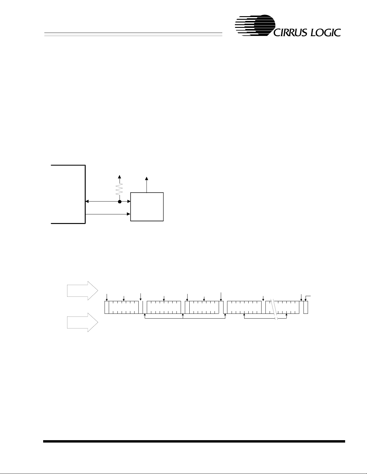
EEPROM INTERFACE
The EEPROM configuration interface allows the connection of an optional external EEPROM device to
provide power-up configuration information. The external EEPROM is not required for proper operation;
however, in some applications power-up configuration settings other than the default values may be required to support specific Operating System compatibility requirements.
After a hardware reset, an internal state machine in the CS4281 will automatically detect the presence of
an external EEPROM device. If the EEPROM header is correct, then EEPROM data is loaded into the Subsystem ID and Subsystem Vendor ID fields at FCh in Configuration Space, along with four bytes of general configuration information loaded into the CFLR register in Configuration Space. If the header data is
invalid, the data transfer is aborted. After power-up, the host can read or write from/to the EEPROM device
by accessing specific registers in the CS4281. Cirrus Logic provides software to read and write the EEPROM.
The two-wire interface for the optional external EEPROM
CS4281
EEDAT
EECLK
Figure 13. External EEPROM Connection
3.3 V 3.3 V
Ω
4.7 k
2-wire
Serial
EEPROM
device address and the byte address of zero. The CS4281 alwa ys begins access at byte address zero and
continues access a byte at a time, using a sequential read, until all needed bytes in the EEPROM are read.
Since only 9 bytes are needed, the smallest EEPROM available will suffice.
device is depicted in Figure 13. During data transfers, the
data line (EEDAT) can change state only while the clock
signal (EECLK) is low. A state change of the data line
while the clock signal is high indicates a start or stop condition to the EEPROM device.
The EEPROM device read access sequence is shown in the
Figure 14. The timing follows that of a random read se-
quence. The CS4281 first performs a “dummy” write operation, then generates a start condition followed by the slave
No
Acknowledge
Stop
CS4280
EEPROM
Part
Start
Address
S
10100000A00000000AS
Write
Bank
Address
Figure 14. EEPROM Read Sequence
Part
Start
Address
10100001
Acknowledge Data
Read
Acknowledge
A
Data DataP1
A
GENERAL PURPOSE I/O PINS
Some CS4281 pins are internally multiplexed to serve different functions depending on the CS4281 driver.
The CS4281 general purpose functionality includes PME# assertion and interrupt functionality. Please
contact Cirrus Logic’s PC Audio support group for more information on the flexibility of the CS4281
GPIO pins.
CIRRUS LOGIC PRODUCT DATA SHEET
DS308PP4 23

PIN DESCRIPTION
CS4281
CrystalClear™ PCI Audio Interface
TEST 51
JACX 52
JACY 53
JBCX 54
JBCY 55
JAB1 56
JAB2 57
JBB1 58
JBB2 59
MIDIIN 60
CVDD[2] 61
CGND[2] 62
MIDIOUT 63
TESTSEL 64
CGND[3] 65
ASDIN2/GPI01 66
PME# 67
VAUX 68
CRYVDD 69
VOLUP 70
VOLDN 71
CRYGND 72
VDD5REF 73
ABITCLK 74
ASDOUT 75
ASDIN 76
ASYNC 77
ARST# 78
EECLK/GPOUT/PCREQ# 79
EEDA T/GPI O2/PCGNT# 80
50 PCIVDD[7]
49 PCIGND[7]
48 AD[0]
47 AD[1]
46 AD[2]
45 AD[3]
44 AD[4]
43 AD[5]
42 AD[6]
41 AD[7]
40 PCIGND[6]
39 PCIVDD[6]
38 C/BE[0]#
37 AD[8]
36 AD[9]
35 AD[10]
34 AD[11]
33 AD[12]
32 AD[13]
31 PCIVDD[5]
30 PCIGND[5]
29 AD[14]
28 AD[15]
27 C/BE[1]#
26 PAR
25 IRQA
24 PERR#
23 STOP#
22 PCIGND[4]
21 PCIVDD[4]
20 DEVSEL#
19 IRQB
18 IRQC
17 TRDY#
16 IRDY#
15 FRAME#
14 C/BE[2]#
13 CGND[1]
100-pin MQFP
CS4281-CM
12 CVDD[1]
11 AD[16]
10 AD[17]
9 AD[18]
8 PCIVDD[3]
7 PCIGND[3]
6 AD[19]
5 AD[20]
4 AD[21]
3 AD[22]
2 AD[23]
1 PCIGND[2]
RST# 82
GNT# 84
PCICLK 83
REQ# 85
AD[31] 88
AD[30] 89
AD[29] 90
AD[28] 91
AD[27] 92
PCIVDD[0] 86
PCIGND[0] 87
CLKRUN# 93
AD[26] 95
AD[25] 96
GPIO3 94
AD[24] 97
IDSEL 99
C/BE[3]# 98
PCIVDD[2] 100
INTA# 81
CIRRUS LOGIC PRODUCT DATA SHEET
24 DS308PP4

CS4281
CrystalClear™ PCI Audio Interface
50 JACY
49 JACX
48 TEST
47 PCIVDD[7]
46 PCIGND[7]
45 AD[0]
44 AD[1]
43 AD[2]
42 AD[3]
41 AD[4]
40 AD[5]
39 AD[6]
38 AD[7]
37 PCIGND[6]
36 PCIVDD[6]
35 C/BE[0]#
34 AD[8]
33 AD[9]
32 AD[10]
31 AD[11]
30 AD[12]
29 AD[13]
28 PCIVDD[5]
27 PCIGND[5]
26 AD[14]
JBCX 51
JBCY 52
JAB1 53
JAB2 54
JBB1 55
JBB2 56
MIDIIN 57
CVDD[2] 58
CGND[2] 59
MIDIOUT 60
TESTSEL 61
CGND[3] 62
ASDIN2/GPIO1 63
PME# 64
VAUX 65
CRYVDD 66
VOLUP 67
VOLDN 68
CRYGND 69
VDD5REF 70
ABITCLK 71
ASDOUT 72
ASDIN 73
ASYNC 74
ARST# 75
25 AD[15]
24 C/BE[1]#
23 PAR
22 IRQA
21 PERR#
20 STOP#
19 PCIGND[4]
18 PCIVDD[4]
17 DEVSEL#
16 IRQB
15 IRQC
14 TRDY#
13 IRDY#
12 FRAME#
11 C/BE[2]#
10 CGND[1]
9 CVDD[1]
100-pin TQFP
CS4281-CQ
8 AD[16]
7 AD[17]
6 AD[18]
5 PCIVDD[3]
4 PCIGND[3]
3 AD[19]
2 AD[20]
1 AD[21]
RST# 79
GNT# 81
INTA# 78
EEDA T/ GPIO2/PCGNT# 77
EECLK/GPOUT/PCREQ# 76
A ‘#’ sign suffix on a pin names indicates an active-low signal.
DS308PP4 25
REQ# 82
PCICLK 80
CIRRUS LOGIC PRODUCT DATA SHEET
AD[31] 85
AD[30] 86
AD[29] 87
AD[28] 88
AD[27] 89
GPIO3 91
AD[26] 92
AD[25] 93
AD[24] 94
PCIVDD[0] 83
PCIGND[0] 84
CLKRUN# 90
C/BE[3]# 95
IDSEL 96
AD[23] 99
AD[22] 100
PCIVDD[2] 97
PCIGND[2] 98

PCI Interface
AD[31:0] - Address/Data Bus, I/O
These pins form the multiplexed address / data bus for the PCI interface.
C/BE[3:0]# - Command Type / Byte Enables, I/O
These four pins are the multiplexed command / byte enables for the PCI interface. During the
address phase of a transaction, these pins indicate cycle type. During the data phases of a
transaction, active low byte enable information for the current data phase is indicated. These
pins are inputs during slave operation and they are outputs during bus mastering operation.
PAR - Parity, I/O
The Parity pin indicates even parity across AD[31:0] and C/BE[ 3:0] for both address and data
phases. The signal is delayed one PCI clock from either the address or data phase for which
parity is generated.
FRAME# - Cycle Frame, I/O
FRAME# is driven by the current PCI bus master to indicate the beginning and duration of a
transaction.
CS4281
CrystalClear™ PCI Audio Interface
IRDY# - Initiator Ready, I/O
IRDY# is driven by the current PCI bus master to indicate that the initiator is ready to transmit
or receive data (complete the current data phase).
TRDY# - Target Ready, I/O
TRDY# is driven by the current PCI bus target to indicate that the target device is ready to
transmit or receive data (complete the current data phase).
STOP# - Transition Stop, I/O
STOP# is driven active by the current PCI bus target to indicate a request to the master to stop
the current transaction.
IDSEL - Initialize Device Select, Input
IDSEL is used as a chip select during PCI Configuration Space read and write cycles.
DEVSEL# - Device Select, I/O
DEVSEL# is driven by the PCI bus target device to indicate that it has decoded the address of
the current transaction as its own chip sele ct range.
REQ# - Master Request, Three-State Output
REQ# indicates to the system arbiter that the CS4281 is requesting access to the PCI bus. This
pin is high-impedance when RST# is active.
GNT# - Master Grant, Input
GNT# is driven by the system arbiter to indicate that CS4281 owns the PCI Bus.
PERR# - Parity Error, I/O
PERR# is used for reporting data parity errors on the PCI bus.
CIRRUS LOGIC PRODUCT DATA SHEET
26 DS308PP4

CS4281
CrystalClear™ PCI Audio Interface
INTA# - Host Interrupt A, Open Drain Output
INTA# is the level triggered interrupt pin dedicated to servicing internal device interrupt
sources.
PCICLK - PCI Bus Clock, Input
PCICLK is the PCI bus clock for timing all PCI transactions. All PCI synchronous signals are
generated and sampled relative to the rising edge of this clock.
RST# - PCI Device Reset, Input
RST# is the PCI bus master reset.
VDD5REF - Clean 5 V Power Supply
VDD5REF is the power connection pin for the 5 V PCI pseudo supply for the PCI bus drivers.
The internal core logic runs on 3.3 Volts. This pin enables the PCI interf ace to support and be
tolerant of 5 Volt signals. For a 5 Volt PCI Bus, VDD5REF must be connected to +5 Volts.
PCIVDD[7:2,0] - PCI Bus Driver Power Supply
PCIVDD pins are the PCI driver power supply pins. These pins must have a nominal
+3.3 Volts.
PCIGND[7:2,0] - PCI Bus Driver Ground Pins
PCIGND pins are the PCI driver ground reference pins.
PME# - PCI Power Management Event, Open Drain, Output
PME# signals a PCI Power Management event. This pin powers up high impedance for
backwards compatibility. It is also backwards compatible since the previous function was a
ground pin. PME# functionality is powered from the VAUX power supply to support D3
wake-up from the AC Link.
CLKRUN# - Optional System Clock Control, I/O, Open Drain
CLKRUN# is an optional PCI signal defined for mobile operations. As an input, high indicates
that the PCICLK is active. The bus controller drives CLKRUN# low when it wants to stop the
PCICLK. As an output, driven low to request that the PCICLK be activated or not stopped. If
not used, this pin must have a weak pull-down attached to keep low. This pin is backwards
compatible since the previous function was a ground pin.
VAUX - PCI Auxiliary Power Supply, Power
Auxiliary 3.3 Volt VDD pin used to maintain limited device funcitonality when the normal
VDD is turned off. This pin is backwards compatible since the previous function was a core
power supply pin with the same voltage.
External Interface Pins
cold
TEST - Test Mode, Input
This pin must be tied to ground.
TESTSEL - Test Mode Select, Input with Pullup
This pin must be left floating or tied to a core power supply pin for normal operation.
CIRRUS LOGIC PRODUCT DATA SHEET
DS308PP4 27

CrystalClear™ PCI Audio Interface
EEDAT/GPIO2/PCGNT# - EEPROM Data Line / PC/PCI Grant, I/O
For expansion card designs, this is the data line for external serial EEPROM containing device
configuration data. When used with an external EEPROM, a 4.7 kΩ pullup resistor is required.
In motherboard designs using PC/PCI, this pin is the PC/PCI serialized grant input. In designs
with neither of the above requirements, this pin can be used as a general purpose input or open
drain output (GPIO2).
EECLK/GPOUT/PCREQ# - EEPROM Clock Line / PC/PCI Request, Output
For expansion card designs, this is the clock line for external serial EEPROM containing
device configuration data. In motherboard designs using PC/PCI, this pin is the PC/PCI
serialized request output. In designs with neither of the above requirements, this pin can be
used as a general purpose output pin (GPOUT).
GPIO3 - General Purpose Input/Output 3, I/O
A general purpose I/O pin that is powered off the PCI power supply. Therefore, this pin does
not support PME# control from the AC link during D3
. This pin powers up in a high
cold
impedance state providing backward compatibility. All general purpose I/O left unused must be
tied high through its own 10 kΩ resistor.
VOLUP - Volume-Up Button, Input
This pin is the volume-up button control input. This pin may also be used as a general purpose
input if its primary function is not needed. Due to the internal 20 kΩ pull-up resistor, if
VOLUP is unconnected, it will be pulled to its inactive state.
CS4281
VOLDN - Volume-Down Button, Input
This pin is the volume-down button control input. This pin may also be used as a general
purpose input if its primary function is not needed. Due to the internal 20 k Ω pull-up resistor, if
VOLDN is unconnected, it will be pulled to its inactive state.
Clock / Miscellaneous
IRQ[A:C] - ISA interrupt pin s, Outputs
These pins can be used in DOS legacy-compatibility mode to bypass the PCI interrupt and use
an ISA interrupt directly. Using these pins can preserve the multi-drop capability of the PCI
interrupt at the expense of another interrupt line. These pins power up high impedance for
backwards compatibility.
CRYVDD - DLL Power Supply
Power pin for internal delay-locked loop. This pin must be connected to a nominal +3.3 Volts.
CRYGND - DLL Ground Supply
Ground pin for internal delay-locked loop.
JACX, JACY, JBCX, JBCY - Joystick A and B X/Y Coordinates, I/O
These pins are the 4 axis coordinates for the joystick port.
JAB1, JAB2, JBB1, JBB2 - Joystick A and B Button Inputs, Input
These pins are the 4 button switch inputs for the joystick port.
CIRRUS LOGIC PRODUCT DATA SHEET
28 DS308PP4

CS4281
CrystalClear™ PCI Audio Interface
MIDIIN - MIDI Data Input
This is the serial input pin for the internal MIDI port. An internal 20 kΩ pull-up resistor will
pull MIDIIN to CVDD.
MIDIOUT - MIDI Data Output
This is the serial output pin for the internal MIDI port.
CVDD[2:1] - Core Power Supply
Core power pins. These pins must be connected to a nominal +3.3 Volts.
CGND[3:1] - Core Ground Supply
Core digital ground reference pins.
Serial Codec Interface
ABITCLK - AC-Link Bit Clock, Input
Master timing clock for serial audio data. This pin is an input which drives the timing for the
AC-Link interface, along with providing the source clock for the CS4281.
ASYNC - AC-Link Frame Sync, Output
Framing clock for serial audio data. This pin is an output which indicates the 48 kHz framing
for the AC-Link. High during slot 0 and low for slots 1 through 12. Also used to induce a
warm reset of the AC-Link when its down.
ASDOUT - AC-Link Data Out, Output
CS4281 serial data out. Provides a register interface and playback audio data path to both the
Primary and Secondary Codecs.
ARST# - AC-Link Reset, Output, Active Low
AC-Link and Codec reset pin. This pin is the logical OR of the PCI reset pin RST# and the
software controlled RSTN bit in the SPMC register. When low, forces all Codecs attached to
the AC Link into a cold reset state.
ASDIN - Primary Codec Data In, Input
Primary Codec’s serial data input to the CS4281 for register reads and capture audio data
streams. This pin is powered from the VAUX power pin to support wake-up events that drive
PME#.
ASDIN2/GPIO1 - Secondary Codec D ata In, Input / General Purpose I/O Pin 1
Secondary Codec’s serial data input to the CS4281 or general purpose input, selected via the
Serial Power Management Control (SPMC) register. This pin is powered from the VAUX
power pin to support wake-up events that drive PME#. As a general purpose I/O pin, it
supports extended capability and PME# (powered from VAUX). If this pin is not used, it
should have an external resistor of 50 kΩ or greater attached to ground (not power).
CIRRUS LOGIC PRODUCT DATA SHEET
DS308PP4 29

PACKAGE OUTLINE
D
CS4281
CrystalClear™ PCI Audio Interface
100-PIN MQFP PACKAGE DRAWING
E
E1
D1
1
e
µ
L
DIM MIN MAX MIN MAX
A ---- 0.134 ---- 3.400
A1 0.010 0.014 0.250 0.350
B 0.009 0.015 0.220 0.380
D 0.667 0.687 16.950 17.450
D1 0.547 0.555 13.900 14.100
E 0.904 0.923 22.950 23.450
E1 0.783 0.791 19.900 20.100
e* 0.022 0.030 0.550 0.750
µ 0.000° 7.000° 0.000° 7.000°
L 0.018 0.030 0.450 0.750
* Nominal pin pitch is 0.65 mm
Controlling dimension is mm.
JEDEC Designation: MS022
B
INCHES MILLIMETERS
A
A1
CIRRUS LOGIC PRODUCT DATA SHEET
30 DS308PP4

CS4281
CrystalClear™ PCI Audio Interface
100-PIN TQFP PACKAGE DRAWING
D1
D
E
E1
1
e
µ
L
DIM MIN MAX MIN MAX
A ---- 0.063 ---- 1.600
A1 0.002 0.006 0.050 0.150
B 0.007 0.011 0.170 0.270
D 0.618 0.642 15.700 16.300
D1 0.547 0.555 13.900 14.100
E 0.618 0.642 15.700 16.300
E1 0.547 0.555 13.900 14.100
e* 0.016 0.024 0.400 0.600
L 0.018 0.030 0.450 0.750
µ 0.000° 7.000° 0.000° 7.000°
* Nominal pin pitch is 0.50 mm
B
INCHES MILLIMETERS
A
A1
Controlling dimension is mm.
JEDEC Designation: MS026
CIRRUS LOGIC PRODUCT DATA SHEET
DS308PP4 31

CS4281
CrystalClear™ PCI Audio Interface
APPENDIX A. MIGRATION FROM A CS4280 DESIGN TO A CS4281 DESIGN
The CS4281-CM is designed to be backward compatible with the CS4280-CM PWB footprint. When the
CS4281 is placed in a CS4280-designed board, the CS4281 will provide the same level of functionality as
the CS4280-CM. The CS4281 is not be available in the 128-pin TQFP package; however, a 100-pin TQFP
package is available for notebook designs. The following descriptions apply only to the 100-pin MQFP
package.
Several supply pins have been redefined on the CS4281. The functionality of two additional pins has been
modified to support additional features. Modified pin definitions default to CS4280 functionality.
Upgraded Pins
• IRQC (pin 18) – replaced CGND[0]
• IRQB (pin 19) – replaced CVDD[0]
• IRQA (pin 25) – replaced SERR#
• TESTSEL (pin 64) – replaced CVDD[3]
• ASDIN2/GPIO1 (pin 66) – replaced GPIO
• PME# (pin 67) – replaced CGND[4]
• VAUX (pin 68) – replaced CVDD[4]
• CLKRUN# (pin 93) – replaced PCIGND[1]
• GPIO3 (pin 94) – replaced PCIVDD[1]
IRQ[A:C] - ISA interrupt pins
Three pins have been redefined as ISA IRQ signals for DOS legacy game support. For
backward compatibility, these pins default to high impedance. Pin 18 will be connected to
ground, pin 19 will be connected to VDD, and Pin 25 will be connected SERR#. High
impedance pins connected to the supply rail results in no damage or excess current being
drawn by that pin. The SERR# pin (25) on the CS4280 has no useful functionality. An audio
device has no condition whereby it must generate a system error. The SERR# pin on the
CS4281 has been eliminated. Pin 25 is held in a high impedance state by power-on default.
TESTSEL - Test Mode Select pin
Pin 64 was formerly a supply pin (CVDD[4]). This pin is designated for selecting test modes
for production testing. This pin must be left floating or tied to a core power supply pin for
normal operation. This pin is tied to CVDD on the CS4280 PWB layout.
ASDIN2/GPIO1 - Secondary Codec D ata In / General Purpose I/O Pi n
The ASDIN2 function is added to the GPIO pin. The function is determined by the AC-Link
configuration setup. The power-up default is the GPIO functionality.
PME# - PCI Power Management Event
The PME# is a new function added to the CS4281. It is an open drained output used to indicate
a power management event. For the CS4280 layout, this pin will be grounded.
VAUX - PCI Auxiliary Power Supply
VAUX maintains limited device functionality when the normal VDD is turned off in the
CS4281. When the CS4281 is used on the CS4280 layout, this pin will be tied to normal VDD.
CIRRUS LOGIC PRODUCT DATA SHEET
32 DS308PP4

CS4281
CrystalClear™ PCI Audio Interface
CLKRUN# - Optional System Clock Control
CLKRUN# is an optional PCI signal defined for mobile operations and is only available on the
CS4280-CQ (128-pin package). This pin is redefined from supply ground to an input with an
open drained output. If maintained at a logic 0, the open drained output is never required to
drive the CLKRUN# signal. In the CS4280 layout, this pin will be tied to ground. Note:
CLKRUN# is not available on the add-in card connector
GPIO3 - General Purpose Input/Output 3
GPIO3 pin of the CS4281 powers up high impedance. High impedance pins connected to the
supply rail results in no damage or excess current being drawn by that pin.
Summary
The new features included in the CS4281 (CLKRUN#, VAUX, TESTSEL, and ISA IRQs) are not usable
when the CS4281 is placed in a CS4280 PWB footprint. The CS4281 maintains the same functionality as
the CS4280 from a user perspective. The CS4281 is NOT backward compatible with the CS4280 software
drivers. A driver upgrade is required to use the CS4281. The upgraded driver will contain support for both
the CS4280 and the CS4281 for those customers that have both devices in their product lines.
For new applications migrating from the CS4280 to the CS4281, several design considerations need attention. Joystick coordinate capacitor values should change from 5.6 nF to 12 nF to more closely approximate
legacy game port timing; however, the CS4281 does approximate the CS4280 timing. The CS4281 does
not support ZV-Port found on the 128-pin version of the CS4280. Full PME capabilities are available on
the CS4281 with the support of Vaux and the PME# functions. CLKRUN# only available on the 128-pin
version of the CS4280 is now available on either the 100-pin MQFP or 100-pin TQFP CS4281. The
CS4281 also supports up to two AC ‘97 Codecs that support the Audio Codec Specification 2.1 extensions.
CIRRUS LOGIC PRODUCT DATA SHEET
DS308PP4 33

CS4281
CrystalClear™ PCI Audio Interface
TEST 51
JACX 52
JACY 53
JBCX 54
JBCY 55
JAB1 56
JAB2 57
JBB1 58
JBB2 59
MIDIIN 60
CVDD[2] 61
CGND[2] 62
MIDIOUT 63
CVDD[3] 64
CGND[3] 65
GPI0 66
CGND[4] 67
CVDD[4] 68
CRYVDD 69
VOLUP 70
VOLDN 71
CRYGND 72
VDD5REF 73
ABITCLK 74
ASDOUT 75
ASDIN 76
ASYNC 77
ARST# 78
EECLK/PCREQ# 79
EEDAT/PCGNT# 80
50 PCIVDD[7]
49 PCIGND[7]
48 AD[0]
47 AD[1]
46 AD[2]
45 AD[3]
TESTSEL
ASDIN2/GPIO1
PME#
VAUX
44 AD[4]
43 AD[5]
42 AD[6]
41 AD[7]
40 PCIGND[6]
39 PCIVDD[6]
38 C/BE[0]#
37 AD[8]
36 AD[9]
35 AD[10]
34 AD[11]
33 AD[12]
32 AD[13]
31 PCIVDD[5]
30 PCIGND[5]
29 AD[14]
28 AD[15]
27 C/BE[1]#
26 PAR
IRQA
IRQB
IRQC
CS4280-CM
CLKRUN#
GPIO3
25 SERR#
24 PERR#
23 STOP#
22 PCIGND[4]
21 PCIVDD[4]
20 DEVSEL#
19 CVDD[0]
18 CGND[0]
17 TRDY#
16 IRDY#
15 FRAME#
14 C/BE[2]#
13 CGND[1]
12 CVDD[1]
11 AD[16]
10 AD[17]
9 AD[18]
8 PCIVDD[3]
7 PCIGND[3]
6 AD[19]
5 AD[20]
4 AD[21]
3 AD[22]
2 AD[23]
1 PCIGND[2]
RST# 82
GNT# 84
PCICLK 83
REQ# 85
AD[31] 88
AD[30] 89
AD[29] 90
AD[28] 91
AD[27] 92
PCIVDD[0] 86
PCIGND[0] 87
AD[26] 95
AD[25] 96
PCIVDD[1] 94
PCIGND[1] 93
IDSEL 99
AD[24] 97
C/BE[3]# 98
PCIVDD[2] 100
INTA# 81
CIRRUS LOGIC PRODUCT DATA SHEET
34 DS308PP4

• Notes •

 Loading...