

Page 1
CS4235
2
2
Advanced Product Databook
FEATURES
■ Compatible with Sound Blaster™, Sound Blaster
Pro™, and Windows Sound System™
■ Advanced MPC3-Compliant Input and Output
Mixer
■ Enhanced Stereo Full Duplex Operation
■ Dual Type-F DMA Support
■ Integrated CrystalCl ear™ 3D Stereo
Enhancement
■ Industry Leading Delta-Sigma Data Converters
(86 dB FS A)
■ Internal Default PnP Resources
■ CS9236 Wavetable Interface
■ CS4610 Audio Accelerator Interface
■ CS4236B/CS4237B/CS4238B Register
Compatible
CrystalClear™
Low Cos t IS A Audi o S yste m
DESCRIPTION
The CS4235 is a single chip multimedia audio system
that is pin-compatible to the CS423xB for many designs. The product includes an integrated FM
synthesizer and a Plug-and-Play interface. In addition,
the CS4235 includes hardware master volume control
pins as well as extensive power management and 3D
sound technology. The CS4235 is compatible with the
Microsoft
run software written to the Sound Blaster and Sound
Blaster Pro interfaces. The CS4235 is fully compliant
with Microsoft’s PC’97 and PC’98 audio requirements.
ORDERING INFO
®
Windows Sound System standard and will
CS4235-JQ 100 pin TQFP, 14x14x1.4mm
CS4235-KQ 100 pin TQFP, 14x14x1.4mm
SD<7:0>
SA<11:0>
IOR
IOW
AEN
IOCHRDY
IRQ<A:G>
DRQ<A:C>
DACK<A:C>
SA<12:15)
(CDROM)
VREFXTALI XTALO
OSCILLATOR VREF
ISA
BUS
INTERFACE
PLUG
AND
PLAY
CODEC
REG
I/F
Config
IO
IRQ
DMA
Decode
Logic
CD-ROM or
Upper Address Bits
FIFO
FIFO
FM
Synthesizer
ANALOG
JOYSTICK
LOGIC
CS4610
INTERFACE
Stereo
ADC1
Stereo
DAC1
Stereo
DAC2
CS9236
WAVETABLE
INTERFACE
INPUT MIXER
Σ
OUTPUT MIXER
MPU-401
UART
with
FIFOS
Σ
WSS
SBPRO
Registers
3D
Enhancement
EEPROM
Interface
GAIN
GAIN
GAIN
ATTN
ATTN
Hardware
Volume Control
L/RAUX1
L/RAUX
CMAUX
MIC
MIN
L/ROUT
UP
DOWN
MUTE
BRESET
JOYSTICK MIDI
SERIAL PORT
NOV ‘97 DS252PP2
SERIAL PORT
Copyright Cirrus Logic, I nc. 1997
(All Rights Reserv ed)
SCL
SDA
Page 2
CrystalClear 16-Bit Audio Motherboard Example Design
TM
TABLE OF CONTENTS
CRD4235-8
CS4235 PERFORMANCE SPECIFICATIONS... 3
GENERAL DESCRIPTION ............... ...... ......... ... 12
ISA Bus Interface ... ......... ...... ......... ...... ...... ...... 13
PLUG AND PLAY........... ......... ...... ......... ......... ... 15
PnP Data ............... ...... ......... ...... ...... ......... ...... 16
Loading Resource Data.............. ...... ......... ...... 16
Loading Firmware Patch Data . ............ ......... ... 18
The Crystal Key........ ...... ...... ......... ...... ......... ... 18
Bypassing Plug and Play ...... ...... ......... ...... ...... 19
Crystal Key 2 .................. ...... ......... ...... ......... ... 20
Hardware Configuration Data........ ......... ......... 20
Hostload Procedure..... ......... ...... ......... ...... ...... 24
External E
2
PROM ........ ...... ...... ......... ...... ......... 25
WINDOWS SOUND SYSTEM CODEC.............. 26
Enhanced Functions (MODEs) ... ......... ......... ... 27
FIFOs............ ...... ......... ...... ......... ...... ...... ......... 27
WSS Codec PIO Register I nterface.......... ...... 27
DMA Interface.. ......... ...... ...... ......... ...... ...... ...... 28
Sound System Codec Register Interface ........ 29
Direct Mapped Registe rs (R0-R3) ............... 30
I/O Data Register s (R3)............. ...... ......... ... 31
Indirect Mapped Regi sters (I0-I31) .............. 32
WSS Extended Registers (X0-X31) ............44
SOUND BLASTER INTERFACE ...... ...... ......... ... 53
Mode Switching ........... ...... ...... ......... ...... ......... 53
Sound Blaster Dire ct Register Interface. ...... ... 53
Sound Blaster Mixer Registers............... ...... ... 54
GAME PORT INTERFACE......... ...... ......... ...... ... 55
CONTROL INTERFACE .... ......... ......... ............ ... 57
Control Register I nterface ..... ...... ...... ......... ...... 57
Control Indirect Registers (C0- C9)............ ...... 59
MPU-401 INTERFACE . ............ ......... ......... ......... 62
MPU-401 Register Interface....... ......... ............ 62
MIDI UART ............... ...... ......... ...... ...... ......... ... 63
MPU-401 "UART" Mode Operatio n........ ......... 63
FM SYNTHESIZER ..................... ...... ......... ...... ... 63
CDROM INTERFACE ........... ......... ...... ...... ......... 64
CS4610 DSP SERIAL DATA PORT ............ ...... 64
CS9236 WAVETABLE SERIAL DATA PORT... 66
WSS CODEC SOFTWARE DESCRIPTION .......67
Calibration .......... ...... ......... ...... ...... ......... ...... .... 67
Changing Sampling Rate ................. ...... ...... .... 68
Changing Audio Data Fo rmats ...... ...... ......... .... 6 9
Audio Data Formats . ............ ......... ......... .......... 69
DMA Registers ..................... ...... ...... ......... ...... . 69
WSS Codec Interrupt .. ......... ......... ............ ....... 71
Error Conditions ....... ......... ...... ...... ......... ...... .... 7 1
DIGITAL HARDWARE DESCRIPTION.. ......... .... 7 2
Bus Interface .................. ...... ......... ...... ...... .......72
Volume Control Interf ace ........... ...... ...... ......... . 72
Crystal/Clock ......... ...... ......... ...... ...... ......... ...... . 73
General Purpose Output Pins.......... ......... ....... 73
Reset and Power Down . ...... ......... ...... ......... .... 7 3
Address Port Configurati on........... ......... ...... .... 73
Multiplexed Pin Co nfiguration ....... ...... ......... .... 7 4
ANALOG HARDWARE DESCRIPTION ............. 74
Line-Level Inputs Plus MPC Mixe r... ...... ......... . 74
Microphone Level Inp ut.. ......... ...... ...... ......... .... 7 5
Mono Input ......... ......... ...... ......... ...... ...... ......... . 75
Line-Level Outputs ............... ...... ......... ...... ...... . 75
Miscellaneous Analo g Signals ......... ...... ......... . 76
GROUNDING AND LAYOUT........... ......... ...... .... 76
POWER SUPPLIES..... ...... ...... ......... ...... ......... ....76
ADC/DAC FILTER RESPONSE . ...... ......... ...... .... 78
PIN DESCRIPTIONS ..................... ......... ...... .......80
ISA Bus Interface Pins...... ...... ......... ...... ......... . 81
Analog Inputs ........ ......... ...... ......... ...... ...... .......82
Analog Outputs ...... ...... ......... ...... ...... ......... ...... . 83
MIDI Interface.............. ...... ......... ...... ......... ...... . 84
External Peripheral Signals.. ...... ...... ......... ...... . 84
Joystick Interf ace ...... ......... ...... ......... ...... ...... .... 85
CS4610 DSP Serial Port Interface ...... ......... .... 8 5
CS9236 Wavetable Serial Port Interface ......... 85
CDROM Interface.. ......... ...... ...... ......... ...... ...... . 86
Volume Control... ......... ......... ............ ......... ....... 87
Miscellaneous.. ...... ......... ...... ...... ......... ...... .......87
Power Supplies ........... ...... ......... ...... ...... ......... . 88
PARAMETER DEFINITIONS... ......... ...... ......... .... 8 9
PACKAGE PARAMETERS.............. ......... ......... . 90
APPENDIX A: DEFAULT PnP DATA. ......... .......91
APPENDIX B: CS4235 DIFFERENCES ... ...... .... 93
Windows 95 and Windows 3.1 are trademarks; Microsoft, Windows and Windows Sound System are registered
trademarks of Microsoft Corporation.
Sound Blaster and Sound Blaster Pro are trademarks of Creative Labs.
Ad Lib is a trademark of Adlib Corporation.
CrystalClear is a trademark of Cir rus Logic, I nc.
2
DS252PP2
Page 3
CrystalClear Low Cost ISA Audio System
TM
CS4235
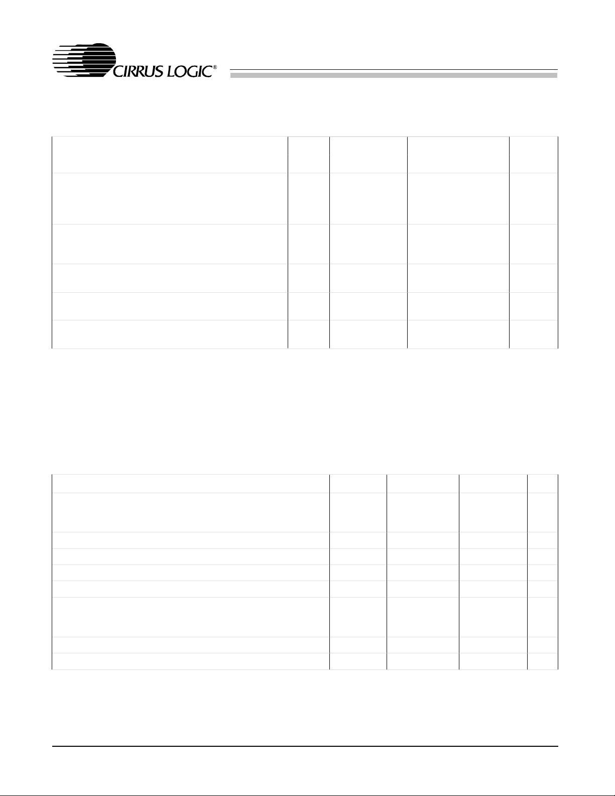
ANALOG CHARACTERISTICS (T
= 25 °C; VA, VD1, VDF1-VDF3 = +5 V;
A
Input Levels: Logic 0 = 0 V, Logic 1 = VD1; 1 kHz Input Sine wave; Sample Frequency, Fs = 44.1 kHz;
Measurement Bandwidth is 20 Hz to 20 kHz, 16-bit linear coding. )
CS4235-JQ CS4235-KQ
Parameter* Symbol Min Typ Max Min Typ Max Units
Analog Input Characteristics (A-D-PC)
- Volume set to 0 dB unless otherwise specified.
ADC1 Resolution (Note 1) 16 - - 16 - - Bits
ADC1 Differential Nonlinearit y (Note 1) - -
Frequency Response: Ac = ±1 dB
Dynamic Range AUX1, AUX2
(Note 2) MIC
Total Harmonic Distortion+Noise AUX1, AUX2
-3 dB FS input (Note 2) MIC
Interchannel Isolat ion (Note 1): Left to Right
10 kHz input AUX1/2 to MIC
AUX1 to AUX2
Interchannel Gain Mismatch AUX1, AUX2
MIC
FR - - - 20 19000 Hz
DR ---80
-75
THD+N ---66
-66
-
-80
-
-80
-
-80
-
-
±0.5
-
-
-
-
-
-
-
-
±0.5
-
±0.5
ADC1 Offset Error 0 dB Gain - - - -
--
-80
-72
-75
-72
-70
-
-
-
-
-85
-80
-80
-80
-80
-80
-90
-
-
±10 ±200
±0.5
-
-
-
-
-
-
-
±0.5
±0.5
LSB
dB FS A
dB FS A
dB FS A
dB FS A
dB
dB
dB
dB
dB
LSB
Full Scale Input Voltage:
(MGE/MBST=1) MIC
(MGE/MBST=0) MIC
AUX1, AUX2, MIN
Gain Drift Input Resistance (Note 1): MIC
AUX1, AUX2, MIN
0.25
2.5
2.5
82011
0.28
2.8
2.8
±100
23
-
0.25
-
-
--
-
-
2.5
2.5
±100
8
20
0.28
2.8
2.8
11
23
-
-
-
V
V
V
-ppm/°C
-
-
kΩ
kΩ
Input Capacitance (Note 1) - - 15 - - 15 pF
Notes: 1. This specification is guaranteed by characterization, no production testing.
2. MGE or MBST = 1 (see WSS Indirect Reg I0 or X2).
pp
pp
pp
*Parameter definitions are given at the end of this data sheet.
Specifications are subject to change without notice.
DS252PP2 3
Page 4
ANALOG CHARACTERISTICS (Continued)
Parameter* Symbol Min Typ Max Min Typ Max Units
CrystalClear Low Cost ISA Audio System
CS4235-JQ CS4235-KQ
TM
CS4235
Analog Output Characteristics (PC-D-A)
DAC1 Resolution (Note 1) 16 - - 16 - - Bits
DAC1 Differential Nonlinearit y (Note 1) - -
DAC1 Frequency Response: Ac = ±1 dB
DAC1 Dynamic Range DR - -86 - -80 -86 - dB FS A
DAC1 Total Harmonic Distort ion+Noise:
-3 dB FS inp ut (Note 3)
DAC1 Interchannel Isolation (Notes 1,3) - -95 - -80 -95 - dB
DAC1 Interchannel Gain Mismatch Voltage Reference Output - VREF 2.0 2.2 2.5 2.0 2.2 2.5 V
Voltage Reference Output Current - VREF
(Notes 1,4)
DAC1 Programmable Attenuation Span 90 94.5 - 90 94.5 - dB
DAC1 Atten. Step Size: Greater than -82.5 dB
-82.5 dB to -94.5 dB
DAC1 Offset Voltage - - - Full Scale Output Voltage (Note 3) 2.5 2.8 3.3 2.5 2.8 3.3 Vpp
Gain Drift (Note 1) - 100 - - 100 - ppm/°C
Deviation from Linear Phase (Note 1)
(Passband)
External Load Impedance (Note 1) 10 - - 10 - Mute A tte nua tio n (Note 1) 80 - - 80 - - dB
- Volume set to 0 dB unless otherwise specified.
±0.5
FR - - - 20 - 19000 Hz
THD+N - -80 - -74 -80 - dB FS A
±0.1 ±0.5
- 100 400 - 100 400
1.3
1.0
- - 1 - - 1 Degr ee
1.5
1.5
1.721.3
--
-
±0.1 ±0.5
1.5
1.0
1.5
±1 ±10
±0.5
1.7
2
LSB
dB
µA
dB
dB
mV
kΩ
Power Supply
Power Supply Current Digital, Operating
Analog, Operating
Total Operating
Total Power Down
Power Supply Rejection, 1 kHz (Note 1) 40 - - 40 - - dB
Notes: 3. 10 kΩ, 100 pF load.
4. DC current only. If dynamic loading exists, then the voltage reference output must be buffered
or the performance of ADCs and DACs will be degraded.
-
-
-
-
70
30
100
-
-
-
-
-
-
70
80
-
30
35
-
100
-
-
-
1
mA
mA
mA
mA
4 DS252PP2
Page 5
CrystalClear Low Cost ISA Audio System
TM
CS4235
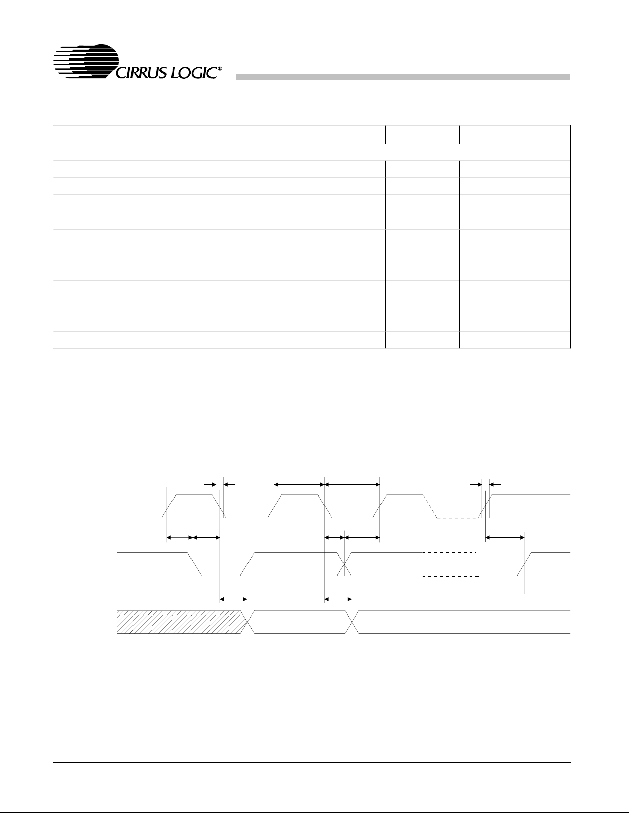
MIXERS (T
1 kHz Inpu t S ine w ave, Me asu remen t B and widt h i s 20 H z t o 20 kHz .)
Mixer Gain Range Span AUX1, AUX2
Step Size MIC, AUX1, AUX2
Frequency Response: Ac = ±1 dB (N otes 1, 3)
(A-A)
Dynamic Range (Notes 1,3)
(A-A)
Total Harmonic Distortion+Nois e (Notes 1,3)
(A-A) -3 dB FS input
= 25 °C; VA, VD1, VDF1-VDF3 = +5 V; Input Levels: Logic 0 = 0 V, Logic 1 = VD1;
A
CS4235-JQ CS4235-KQ
Parameter* Symb ol Min T yp Max Min Typ Max Units
-
MIC
Hardware Master
DAC1, DAC2
Hardware Master
DAC1, DAC2
FR - - - 20 - 20000 Hz
DR - -88 - -90 -97 - dB FS A
THD+N - -85 - -85 -90 - dB FS A
-
-
-
-
-
-
--
-
-
-
-
-
-
-
-
-
42
40
75
85
1.3
1.6
0.9
45
45
86
94.5
1.5
2.0
1.5
-
-
-
-
1.7
2.4
2.0
dB
dB
dB
dB
dB
dB
dB
ABSOLUTE MAXIMUM RATINGS (AGND, DGND, SGND = 0 V, all voltages with respect to 0 V.)
Parameter Symbol Min Max Units
Power Supplies: Digital
Analog
Total Power Dissipation (Supplies, In puts, Outputs) - 1 W
Input Current per Pin (Except Supply Pins) -10.0 +10.0 mA
Outpu t Cu rren t pe r P in (Exce pt S upp ly P ins) -50 +50 mA
Analog Input Voltage -0.3 VA+0.3 V
Digital Input Voltage: SA<15:0>, IOR, IOW, AEN
SD<7:0>, DACK<A:C>
All other digital inputs
Ambient Temperature (Power Applied) -55 +125 °C
Storage Temperature -65 +150 °C
Warning: Operation beyond these limits may result in permanent damage to the device.
Normal operation is not guaranteed at these extremes.
DS252PP2 5
VD1
VDF1-VDF3
VA
-0.3
-0.3
-0.3
-0.3
-0.3
6.0
6.0
6.0
VD1+0.3
VDF+0.3
V
V
V
V
V
Page 6
RECOMMENDED OPERATING CONDITIONS
(AGND, DGND, SGND = 0 V, a ll voltages with r espect to 0 V.)
Parameter Symbol Min Typ Max Unit s
CrystalClear Low Cost ISA Audio System
TM
CS4235
Power Supplies: Digital (Note 5)
Digital Filtered
Analog
Operating Ambient Temperature T
VD1
VDF1-VDF3
VA
A
4.75
4.75
4.75
5.0
5.0
5.0
5.25
5.25
5.25
02570°C
Note 5: VD1 su pplie s the pow er to th e ISA in terf ace pins .
ADC1/DAC1 DIGITAL FILTER CHARACTERISTICS (Not e 1)
Parameter Symbol M in Typ Max Units
Passband 0 - 0.40xFs Hz
Frequency Response -1.0 - +0.5 dB
Passband Ripple (0-0.40xFs) - -
±0.1
Transition Band 0.40xFs - 0.60xFs Hz
Stop Band 0.60xFs - - Hz
Stop Band Rejection 74 - - dB
Group Delay - - 10/Fs s
Group Delay Variation vs. Frequency ADC1
DAC1
-
-
-
-
0.0
0.1/Fs
dB
V
V
V
µs
µs
DIGITAL CHARACTERISTICS
= 25 °C; VA, VDF1-VDF3 = +5 V, VD1 = +5 V; AGND, DGND1, SGND1-SGND4 = 0 V.)
(T
A
Parameter Symbol Min Max Units
High-level Input Voltage UP/DOWN/MUTE
Other Digital Inputs
XTALI
Low-level Input Voltage V
High-level Output Voltage: ISA Bus Pins I0 = -24. 0 mA
V
IOCHRDY, SDA (Note 6)
All Others I0 = -1.0 mA
Low-level Output Voltage: ISA Bus Pins I0 = 24.0 mA
V
MCLK, SDOUT, MIDOUT, IOCHRDY I0 = 8.0 mA
All Others I0 = 4.0 mA
V
IH
IL
OH
OL
3.0
2.0
VDF-1.0
-0.8V
2.4
-
2.4
-
-
Input Leakage Current (Digital Inputs) -10 10
Output Leakage Curr ent (High-Z Digital Outputs) -10 10
Note 6. Open Collector pins. High level output voltage dependent on external pull up (required) used and
number of per ipherals (gat es) attached.
6 DS252PP2
-
-
-
VD1
VDF
VDF
0.4
0.4
0.4
V
V
V
V
V
V
V
V
V
µA
µA
Page 7
CrystalClear Low Cost ISA Audio System
TM
CS4235
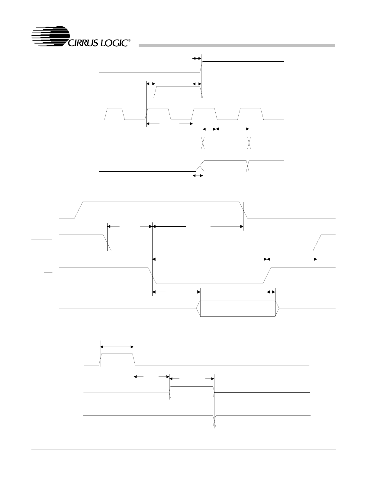
Timing Parameters (T
= 25 °C; VA, VD1, VDF1-VDF3 = +5 V; outputs loaded with 30 pF;
A
Input Levels: Logic 0 = 0 V, Logic 1 = VDF, Rise/Fall time = 2 ns; Input/Output reference levels = 2.5 V)
Parameter Symbol Min Max Units
E2PROM Timing
SCL Low to SDA Data Out Valid t
Start Condition Hold Time t
Clock Low Period t
Clock High Period t
Start Condition Setup Time (for a Repeated Start Condition) t
Data In Hold Time t
Data In Setup Time t
SDA and SCL Ris e Time (Note 7) t
SDA and SCL Fall Time t
Stop Condition Setup Time t
Data Out Hold Time t
(Note 1)
AA
HD:STA
LSCL
HSCL
SU:STA
HD:DAT
SU:DAT
R
F
SU:STO
DH
03.5
4.0 -
4.7 -
4.0 -
4.7 0-
µs
µs
µs
µs
µs
µs
250 - ns
-1
µs
- 300 ns
4.7 -
µs
0-ns
Notes 7. Rise time on SDA is determined by the capacitance of the SDA line with all connected gates and the
exter nal pul lup re sisto r requi red.
t
t
F
HSCL
t
LSCL
t
R
SCL
t
SU:STA
t
HD:STA
t
HD:DAT
t
SU:DAT
t
SU:STO
SDA (IN)
t
AA
t
DH
SDA (OUT)
E2PROM 2-Wire Interface Timing
DS252PP2 7
Page 8

TIMING PARAMETERS (Continued)
Parameter Symbol Min Max Units
Paral lel Bu s Ti min g
CrystalClear Low Cost ISA Audio System
TM
CS4235
IOW or IOR strobe width t
Data valid to IOW rising edge (write cycle) t
IOR falling edge to data valid (read cycle) t
SA <> and AEN setup to IOR or IOW fa lling edge t
SA <> and AEN hold from IOW or IOR rising edge t
DACK<> inactive to IOW or IOR falling edge ( DMA cycle
immedi atel y f ollo wed by a no n-DM A cyc le ) (Not e 8)
DACK<> active from IOW or IOR rising edge (non-DMA
cycle completion followed by DMA cycle) (Note 8)
DACK<> setup to IOR fa lling edge (DMA cycle s)
DACK<> setup to IOW fallin g edge (Note 8)
Data hold from IOW rising edge t
DRQ<> hold from IOW or IOR falling edge DTM(I10) = 0
(assumes no more DMA cycles needed) DTM(I10) = 1
Time between rising edge of IOW or IOR to ne xt falling
edge of IOW or IOR
Data hold from IOR rising edge t
DACK<> hold from IOW rising edge
DACK<> hold from IOR rising edge
STW
WDSU
RDDV
ADSU
ADHD
t
SUDK1
t
SUDK2
t
DKSUa
t
DKSUb
DHD2
t
DRHD
t
BWDN
DHD1
t
DKHDa
t
DKHDb
90 - ns
22 - ns
-60ns
22 - ns
10 - ns
60 - ns
0-ns
25
25
-
-
ns
ns
15 - ns
-
-25
45
ns
-
80 - ns
025ns
25
25
-
-
ns
ns
RESDRV puls e width hi gh (Note 1) t
RESDRV
Initialization Time (Note 1, 9) t
EEPROM Read Time (Note 1, 10) t
EEPROM
INIT
1-ms
310ms
1190ms
XTAL, 16.9344 MHz, frequency (Notes 1, 11) 16.92 16.95 MHz
XTALI high time (Notes 1, 11) 24 - ns
XTALI low time (Notes 1, 11) 24 - ns
Sampl e Frequ ency (Note 1) F s 3.91 8 50 k Hz
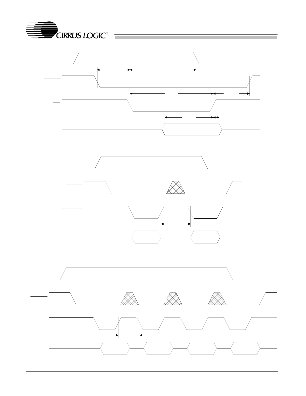
CS4610 DSP Serial Port Timing
SCLK r isin g t o SD OUT v al id (Note 1) t
SCLK rising to FSYNC transition (Note 1) t
SDIN valid to SCLK falling (Note 1) t
SDIN hold after SCLK falling (Note 1) t
PD1
PD2
S1
H1
-60ns
-20 2 0 ns
30 - ns
30 - ns
Notes: 8. AEN must be high during DMA cycles.
9. I nitialization time depends on the power supply circuitry, as well as the the type of clock used.
10. EEPROM read time is dependent on amount of data in EEPROM. Minimum time relates to no
EEPROM present. Maximum time relates to EEPROM data size of 1k bytes.
11. The Sample frequency specification must not be exceeded.
8 DS252PP2
Page 9
FSYNC
SF1,0=01,10
t
pd2
CrystalClear Low Cost ISA Audio System
TM
CS4235
DRQ<>
DACK<>
FSYNC
SCLK
SDIN
SDOUT
SF1,0=00
t
DKSUa
t
pd2
t
sckw
t
pd1
CS4610 DSP Seri al Port Timing
t
DRHD
t
pd2
t
s1
MSB, Left
MSB, Left
t
STW
t
h1
t
DKHDb
IOR
SD<7:0>
RESDRV
SCL/SDA
SD<>
SA<>
t
RDDV
8-Bit Mono DMA Read/Capture Cycl e
t
RESDRV
t
INIT
t
EEPROM
EEPROM read
Cod ec respo nd s to ISA activity
Reset Timing
t
DHD1
DS252PP2 9
Page 10
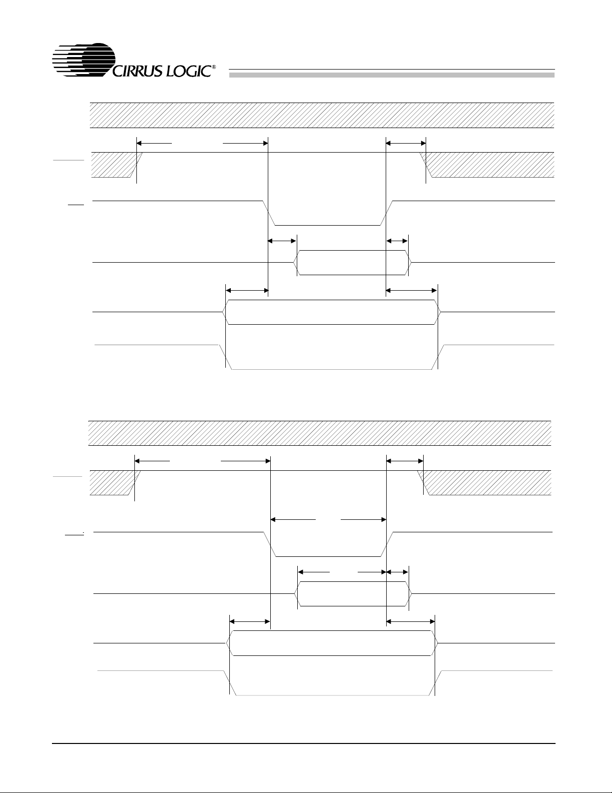
DRQ<>
CrystalClear Low Cost ISA Audio System
TM
CS4235
DACK<>
IOW
SD<7: 0>
DRQ<>
DACK<>
IOR/IOW
t
DKSUb
t
DRHD
t
STW
t
WDSU
8-Bit Mono DMA Write/Playback Cycle
t
DHD2
t
DKHDa
DRQ<>
DACK<>
IOR/IOW
SD<7:0>
SD<7 :0>
t
BWDN
LEFT/LOW
BYTE
8-Bit Stereo or 16-Bi t Mono DMA Cycle
t
BWDN
LEFT/LOW
BYTE
LEFT/HIGH
BYTE
16-Bit Stereo DMA Cycle
RIGHT/HIGH
BYTE
RIGHT/LOW
BYTE
RIGHT/HIGH
BYTE
10 DS252PP2
Page 11
DRQ<>
CrystalClear Low Cost ISA Audio System
TM
CS4235
DACK<>
IOR
SD<>
SA<>
AEN
t
SUDK1
t
RDDV
t
ADSU
I/O Read Cycle
t
SUDK2
t
DHD1
t
ADHD
DRQ<>
DACK<>
IOW
SD<>
SA<>
AEN
t
SUDK1
t
STW
t
ADSU
I/O Write Cycle
t
WDSU
t
SUDK2
t
DHD2
t
ADHD
DS252PP2 11
Page 12

CrystalClear Low Cost ISA Audio System
TM
CS4235
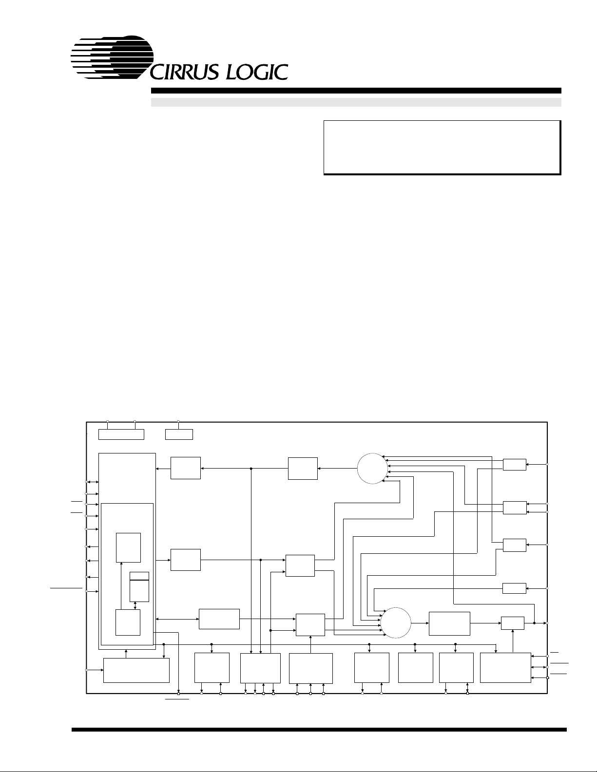
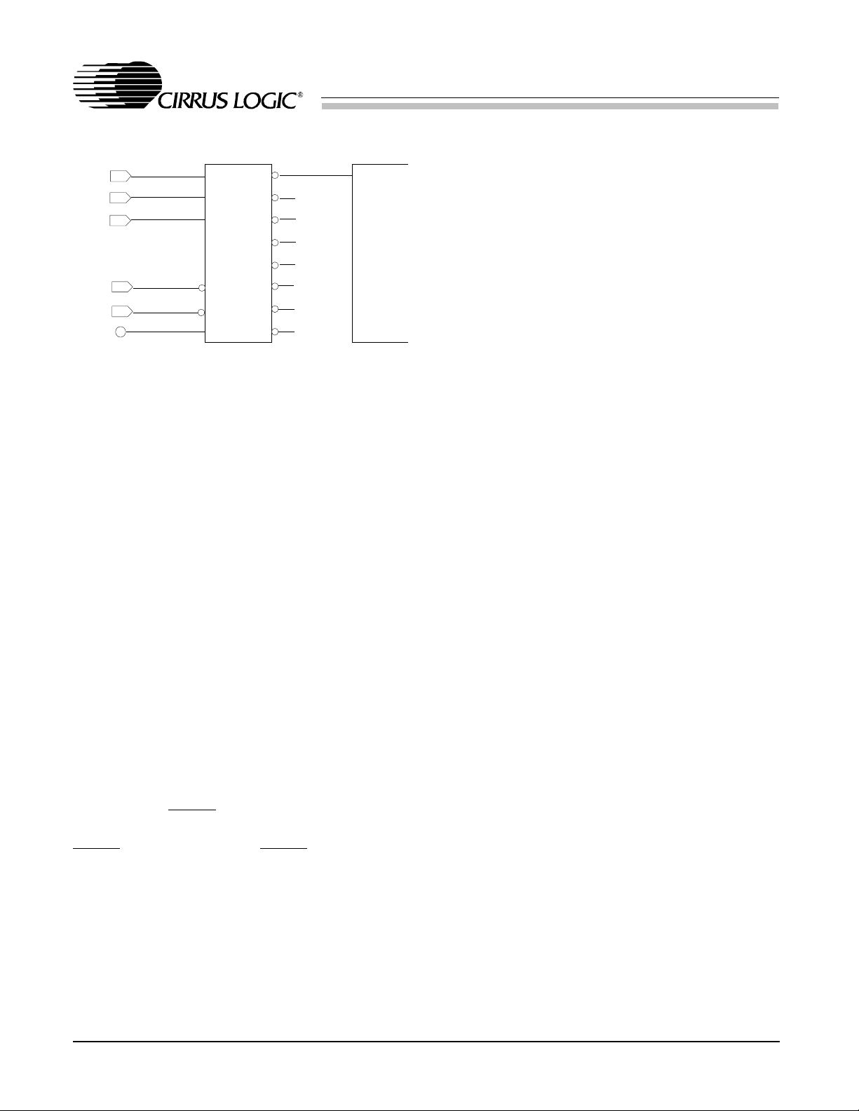
GENERAL DESCRIPTION
This device i s comprised of six phys ical devices
along with Plug-and-Play support for one additional extern al device. The intern al devices ar e:
Windows Sound System Codec
Sound Blaster Pro Compatibl e Interface
Game Port (Joystick)
Control
MPU-401
FM Synthesizer
The external device is :
IDE CDROM
On power up, this part requires a RESDRV signal to initialize the internal configuration. When
initially p owered up, the p art is isolate d from the
bus, and each d evice supported by the part must
be activated via software. Once activated, each
device responds to the resources given (Address,
IRQ, and DMA channels). The devices listed
above are grouped into five logical devices, as
shown in Figure 1 (bracketed features are supported, but typically not used). The five logical
devices are:
LOGICAL DEVICE 0:
Windows Sound System Codec (WSS Codec)
Adlib/Sound Bl aster-compatible Synt hesizer
Sound Blaste r Pro Compati ble Interf ace
LOGICAL DEVICE 1: Game Port
LOGICAL DEVICE 2: Control
LOGICAL DEVICE 3: MPU401
Interrupts and DMA channels. The WSS Codec,
FM synthesizer, and the SBPro compatible devices are in ternal t o the part.
Logical Dev ice 1 is the Game Port that supports
up to two joysti ck devices.
Logical Device 2 is the Control device that supports global features of t he part. Th is device u ses
I/O locations to control power management,
joystick rate, and PnP resource data load ing.
Logical Device 3 is the MPU-401 interface. The
MPU-401 MIDI interface includes a 16-byte
FIFO for data transmitted out the MIDOUT pin
and a 16-byte FIFO for data received from the
MIDIN pin.
Logical Device 4 supports an IDE CDROM device. Although this logical device is listed as a
CDROM, any exte rnal device that fits within the
resources listed above may be substituted. This
interface, is generic and can support devices using 1 to 127 I/O loc ations for the base ad dress, 1
to 8 I/O locat ions for the alternate base address,
an interrupt, and a DMA channel.
ISA Bus Interface
The 8-bit parallel I/O and 8-bit parallel DMA
ports provide an interface which is compatible
with the Industry Standard Architecture (ISA)
bus. The ISA Interface enables the host to communicate with the various functional blocks
within the part via two types of accesses: Programmed I/O ( PIO) acce ss, and DMA access.
LOGICAL DEVICE 4: CDROM
Logical Device 0 consists of three physical devices. The WSS Codec and the Synthesizer are
grouped together since the original Windows
Sound System card expected an FM synthesizer
if the codec was pre sent. The Sound Blaster Pro
Compatible interface, SBPro, is also grouped to
allow the WSS Codec and the SBPro to share
12
A number of configuration registers must be programmed prior to any accesses by the host
computer. The configuration registers are programmed via a Plug-and-Play configuration
sequence or via configuration software provided
by Cirrus Logic.
DS252PP2
Page 13

PnP ISA Bus
Interface
CrystalClear Low Cost ISA Audio System
TM
CS4235
Logical Device 0
WSS Codec:
I/O: WSSbase
2 DMA Chan.
1 Interrupt
Logical Device 1
Game Port:
I/O: GAMEbase
Logical Device 2
I/O: CTRLbase
[1 Interrupt]
Figure 1. Lo gi cal De vices
Synthesis:
I/O: SYNbase
[1 Interrupt]
SBPro:
I/O: SBbase
(DMA shared)
(Interrupt shared)
I/O CYCLES
Every devic e that is enabled, requires I/O space.
An I/O cycle begins when the part decodes a
valid address on the bus while the DMA acknowledge signals are inactive and AEN is low.
The
IOR and IOW signals determine the direction of the data tr ansfer. For read cycles, the par t
will drive data on the SD<7:0> lines while the
host a sserts the
IOR strobe. Write cycles require
the host to assert data on the SD<7:0> lines and
strobe the
ing edge of the
IOW signal. Data is latched on the ris-
IOW strobe.
I/O ADDRESS DECODING
The logical devices use 10-bit or 12-bit address
decoding. The Synthesizer, Sound Blaster, Game
Control:
Logical Device 3
MPU-401:
I/O: MPUbase
1 Interrupt
Logical Device 4
CDROM:
I/O:
CDbase
ACDbase
[1 Interrupt]
[1 DMA Chan.]
Port, MPU-401, and CDROM devices support
10-bit address decoding, while the Windows
Sound System and Control devices support 12bit addres s decoding. Devi ces that support 10-b it
address decoding, require A10 and A11 be zero
for proper decode; therefore, no aliasing occurs
through t he 12-bi t address sp ace.
To p revent aliasing into the upper address space,
a "16-bit decode" opt ion may be used, where the
upper address bits SA12 through SA15 are connected to the part. SA12 -SA15 are then decod ed
to be 0,0,0,0 for all logical device address decoding. When the upper address bits are used,
the CDROM interface is no longer available
since the upper address pins are multiplexed
with the CDROM pins (See Reset and Power
Down section). If the CDROM is needed, the
circuit shown in Figure 2 can replace the SA12
through SA15 pins and provide the same functionality. Four cascaded OR gates, using a
74ALS32, can replace the ALS138 in Figure 2,
but causes a gr eater delay in add ress decoding .
DS252PP2
13
Page 14
CrystalClear Low Cost ISA Audio System
TM
CS4235
ISA Bus
SA12
SA13
SA14
SA15
AEN
+5V
Figure 2 . 16 -b it Dec ode Circ uit
74ALS138
1
A
2
B
3
C
4
G2A
5
G2B
6
G1
Y0
Y1
Y2
Y3
Y4
Y5
Y6
Y7
15
AEN
DMA CYCLES
The part supports up to three 8-bit ISA-compatible DMA channels. The default hardware
connections, which can be changed through the
hardware conf iguration d ata, are:
D M A A = I SA DMA channel 0
D M A B = I SA DMA c han nel 1
D M A C = I SA DMA c han nel 3
The typical configuration would require two
DMA channels. One for the WSS Codec and
Sound Blaster playback, and the other for WSS
Codec capture (to support full-duplex). The
CDROM, if used, can also su pport a DMA channel, although t his is not ty pical.
DMA cycles are distinguished from control register cycles by the generation of a DRQ (DMA
Request). The host acknowledges the request by
generating a
DACK (DMA Acknowledge) signal. The t ransfer of audio data occurs during the
DACK cycle. During the DACK cycle the address lines are ign ored.
The digital audio data interface uses DMA request/grant pins to transfer the digital audio data
between the part and the ISA bus. Upon receipt
of a DMA request, the host processor responds
with an acknowledge signal and a command
strobe which tran sfers data to and from the part,
eight bits at a time. The request pin stays active
until the ap propriate number of 8-bit cycles have
occurred. The number of 8-bit tran sfers will vary
depending on the digital audio data format, bit
resolution, and o peration mode.
The DMA request signal can be asserted at any
time. Once asserted, the DMA request will remain asserted until a complete DMA cycle
occurs. A complete DMA cycle consists of one
or more bytes depending on which device internal to the pa rt is generatin g the request.
INTERRUPTS
For Plug-and-Play flexibility, seven interrupt
pins are supported, although only one or two are
typically used. The default hardware connections, which can be modified through the
hardware config uration data, are:
IRQ A = ISA Interrupt 5
IRQ B = ISA Interrupt 7
IRQ C = ISA Interrupt 9
IRQ D = ISA In terrupt 11
IRQ E = ISA Interrupt 12
IRQ F = ISA In terrupt 15
IRQ G is new and defaults to not being connected for backwards compatibility. This new
interrupt pin would typically be connected to
ISA Interrupt 10. New designs that use IRQ G
must change the Hardware Configuration Data to
indicate which ISA Interrupt is connected to
IRQ G.
The typical configuration would support two interrupt sources: one shared between the WSS
Codec and the Sound Blaster Pro co mpatible devices, and the other for the MPU401 device.
Interrupts are also supported for th e FM Synthesizer, Control, and CDROM devices, but are
typically n ot used.
14
DS252PP2
Page 15

CrystalClear Low Cost ISA Audio System
TM
CS4235
PLUG AND PLAY
The Plug-and-Play (PnP) interface logic is compatible with the Intel/Microsoft Plug-and-Play
specification, version 1.0a, for an ISA-bus device. Since the part is an ISA-bus device, it only
supports ISA-compatible IRQs and DMA channels. Plug and Play compatibility allows the PC
to automatically configure the part into the system upon power up. Plug and Play capability
optimally resolves conflicts between Plug and
Play and non-Plug and Play devices within the
system. Alternatively, the PnP feature can be bypassed. See the Bypassing PnP section for more
information. For a detailed Plug-and-Play protocol description, please refer to the Plug and Play
ISA Specifica tion.
To s upport Plug-and-Play in ISA systems that do
not have a PnP BIOS or a PnP-aware operating
system, the Configuration Manager (CM) TSR
and an ISA Configuration Utility (ICU) from Intel Corp. are used to provide these functions.
The CM isolates the cards, assigns Card Select
Numbers, reads PnP card resource requirements,
and allocates resources to the cards based on
system resource availability. The ICU is used to
keep the BIOS and t he CM informed of the current system configuration. It also aids users in
determining configurations for non-PnP ISA
cards. A more thorough discussion of the Configuration Manager and the ISA Configuration
Utility can be found in the Product Development
Information document of the Plug and Play Kit
by Intel Corp. In a PnP BIOS system, the BIOS
is responsible for configuring all system board
PnP devices. Some systems require additional
software to aid the BIOS in co nfiguring PnP ISA
cards. The PnP BIOS can execute all PnP functions independently of the type of operating
system. However, if a PnP aware operating system is present, the PnP responsibilities are s hared
between the BIOS and the ope rating system. For
more information regarding PnP BIOS, please
refer to the latest revision of the Plug and Play
BIOS Specification published by Compaq Computer, Phoenix Technologies, and Intel.
The Plug and Play configuration sequence maps
the various functional blocks of the part (logical
devices) into the host system address space and
configures both th e DMA and interru pt channels.
The host has access to the part via three 8-bit
auto-configuration ports: Address port (0279h),
Write Data port (0A79h), and relocatable Read
Data port (020Bh - 03FFh ). The read data port is
relocated automatically by PnP software when a
conflict occurs. Note that the Address Port can
be moved for motherboard devices. See the Ad-
dress Port Configuration section for more
details.
The configu ration sequen ce is as fo llows:
1. Host send s a software key whic h places all
PnP cards in the sleep state (or Plug-andPlay mode).
2. The CS4 235 is isola ted from the sy stem using
an isolation s equence.
3. A unique identifier (h andle) is ass igned to t he
part and the reso urce data is read.
4. After all cards’ resource requirements are de-
termined, the host uses the handle to assign
conflict- free resour ces
5. After the c onfiguration reg isters have been
programmed, e ach configu red logical device
is activated.
6. The part is then removed from Plug-and-Pla y
mode.
Upon power-up, th e chip is inactive and must be
enabled via software. The CS4235 monitors
writes to the Address Port . If the host sends a
PnP initiation key, consisting of a series of 32
predefined byte writes, the hardware will detect
DS252PP2
15
Page 16

CrystalClear Low Cost ISA Audio System
TM
CS4235
the key an d place the part into the Plug-and-Pla y
(PnP) mode. Another method to prog ram the part
is to use a special Crystal initiation key which
functions like the PnP initiation key, but can be
invoked by the user at any time. However, the
Crystal Key only supports one Audio Codec per
system. The Crystal key and special commands
are detailed in the Crystal Key and Bypassing
PnP sections.
The isolation sequence uses a unique 72-bit serial identifier. The host performs 72 pairs of I/O
read accesses to the Read Data port. The identifier determines what data is put on the data bus
in respons e to th ose read acc esses. When the isolation sequence is complete, the CM assigns a
Card Select Number (CSN) to the part. This
number distingu ishes the CS4235 from the other
PnP devices in the system. The Configuration
Manager (CM) then reads t he resource data from
the CS4235. The 72-bit identifier and the resource data is either stored in an external
user-programmable E
2
PROM, or loaded via a
"hostload" procedure from BIOS before PnP
software is initi ated.
The CM determines the necessary resource requirements fo r the system and then pr ograms the
part through the configurat ion registers . The configuration register data is written one logical
device at a time. After all logical devices have
been configured , CM activates each device individually. Each logical device is now availa ble on
the ISA bus and responds to the programmed
address rang e, DMA channels, and interrup ts that
have been all ocated to t hat logical de vice.
PnP Data
Hardware Configuration and Plug-and-Play re-
source data can be loaded into the part’s RAM.
The data may be stored in an external E
2
PROM
or may be downloaded from the host. Internal
default PnP data is provided for motherboard designs.
To load the data, refer to the Loading Resource
Data section. The following is the Plug-and-Play
resource data:
The first nine bytes of the PnP resource data are
the Plug-and-Play ID, which uniquely identifies
the Audio Codec from other PnP devices. The
PnP ID is broken down as follows:
0Eh, 63h - Crystal ID - ’CSC’ in compressed
ASCII. (See the PnP Spec for more
information)
42h - OEM ID. A unique OEM ID must be ob-
tained from Crystal for e ach unique
Crystal product used .
25h - Crystal produc t ID for the CS4235
FFh, FFh, FFh, FFh - Serial number. This can
be modified by each OE M to uniquel y
identify their card.
??h - Checksum.
Of the 9-byte serial number listed above, Cirrus
software uses the first two bytes to indicate the
presence of a CS4235, and the fourth byte, 0x25 ,
to indicate the CS4235; therefore, these three
bytes must not b e altered. The de fault PnP ID, in
hex, is 0E634236FFFFFFFFA9 for backwards
compatibility.
The next 3 bytes are the PnP version number.
The default is versio n 1.0a: 0Ah , 10h, 05h.
The next seque nce of bytes are the ANSI i dentifier string. The default is: 82h, 0Eh, 00h,
’Crystal Cod ec’, 00h.
The logical device data must be entered using
the PnP ISA Specification for mat. Typical logical
device values are found in Table 1. Internal default E
2
PROM data is found in Appendix A.
Loading Resource Data
2
A s e r i al E
PROM interface allo ws user-programmable serial number and resource data to be
stored in an external E
2
PROM. The interface is
compatible with devices from a number of ven-
16
DS252PP2
Page 17
CrystalClear Low Cost ISA Audio System
TM
CS4235
dors and th e size may vary accor ding to specific
customer requirements. The maximum size for
resource data supported by the part’s internal
RAM is 384 bytes of combined Hardware Configuration and PnP resource data. With the
addition of the 4-byte header, the maximum
amount of E
2
PROM space used would be 388
bytes. However, the part also supports firmware
upgrades v ia the E
upgrades, t he E
2
PROM. To support firmware
2
PROM size must be great er than
770 bytes. After power-up, the existence of an
2
E
PROM is checked by reading the first two
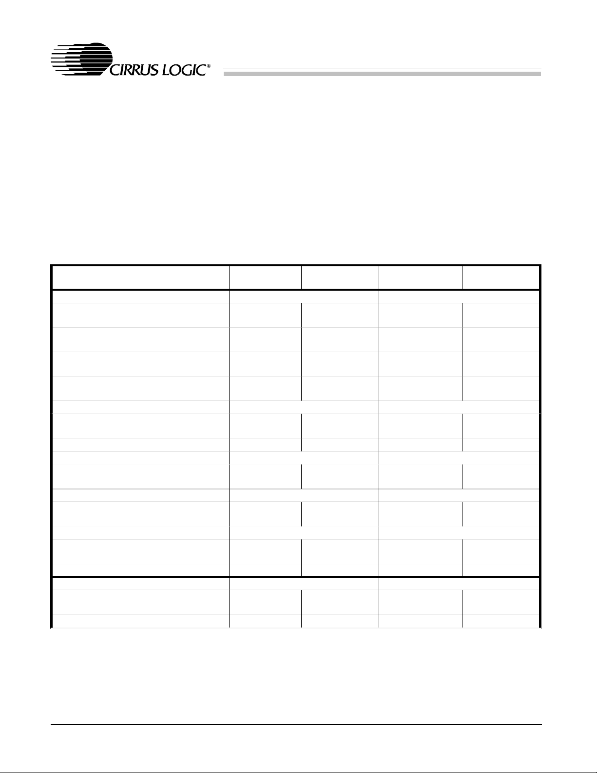
Physical Device Logical Device Best Choice Acceptable
WSS 0 ANSI ID = CSC0000 ANSI ID = WSS/SB
16-bit address
decode
high true
edge sensitive
8-bit, count by
byte, type A
same DMA1
Synthesis 0
16-bit address
decode
SB Pro 0
16-bit address
decode
Game Port 1 ANSI ID = CSC0001 ANSI ID = GAME
16-bit address
decode
Control 2 ANSI ID = CSC0010 ANSI ID = CTRL
16-bit address
decode
MPU401 3 ANSI ID = CSC0003 ANSI ID = MPU
16-bit address
decode
WSSbase
Length/Alignment
IRQ 5
DMA0
(playback)
(record)
SYNbase
Length/Alignment
IRQ ---- ---- --- -
SBbase
Length/Alignment
GAMEbase
Length/Alignment
CTRLbase
Length/Alignment
IRQ ----
MPUbase
Length/Alignment
IRQ 9 9,11,12,15 ----
534h
4/4
(SB share)
1
(SB share)
0, 3 0, 1, 3 ----
388h
4/8
220h
16/32
200h
8/8
120-FF8h
8/8
330h
2/8
bytes from the E
two bytes from the E
BBh, then the rest of the E
loaded into the internal RAM. If the first two
bytes are n’t correct, the E
to exist. For motherboard designs, internal default PnP data is provided or a Hostload
sequence can be used to update the resource
data. If the part is installed on a plug-in card,
then an external E
that the proper PnP resource data is loaded into
the internal RAM prior to a PnP sequence. See
Choice 1
534-FFCh
4/4
5,7,9,11,12,15
(SB share)
1, 3
(SB share)
388h
4/8
220-260h
16/32
208h
8/8
330-360h
2/8
2
PROM interface. If the first
2
PROM port read 55h and
2
PROM is assumed not
2
PROM is required to ensure
Sub opti mal
Choice 1
534-FFCh
4/4
5, 7, 9, 11, 12, 15
(SB share)
0, 1, 3
(SB share)
388-3F8h
4/8
220-300h
16/32
330-3E0h
2/8
2
PROM data is
Sub optimal
Choice 2
---- Feature not supported in the listed configuration, but is supported through customization.
Table 1. Typ ical Moth erboard Pl ug-and- Play Reso urce Data
DS252PP2
17
Page 18

CrystalClear Low Cost ISA Audio System
TM
CS4235
the External E2PROM section for more information on the serial E
2
E
PROM programming.
The format for the data stored in the E
2
PROM interface and
2
PROM is
as follows:
2 bytes E
2 bytes length o f resource data i n E
2
PROM validation: 55h , BBh
2
PROM
19 bytes Hardware Co nfiguration
9 bytes Plug and Play ID
3 bytes Plug and Play v ersion number
Variable number of bytes of user defined
ASCII ID string
Logical Device 0 (Windows Sound System,
FM Synthesizer, Sound Blaster Pro) data
patches in E
2
PROM, gives the maximum functionality at power-up without the need for a
software driver.
The firmware patch data is typically included at
the end of th e PnP resource data. Cirrus provide s
a utility that will read in patch data from a file,
and append it to the PnP resource data. The
patch file must be obt ained from Cirrus.
The Crystal K ey
NOTE: The Crystal Key cannot differentiate between mult iple Cirrus Au dio Codec s in a sys tem;
therefore, ONLY ONE audio part is allowed in
systems using th e Crystal Key. To allow multiple
parts in a system, the Plug-and-Play isolation sequence must be used since it supports multiple
parts via the serial identifier used in the isolation
sequence. Crystal Key 2 is also designed to allow motherboard and add-in card chips to
co-exist in a system.
Logical Device 1 ( Game Port) data
Logical Device 2 ( Control) dat a
Logical Device 3 ( MPU-401) data
Logical Device 4 ( CD-ROM) data
End of Resource b yte & checksum byt e
Firmware patch code.
The default internal E
2
PROM data, in assembly
format, can be found in Appendix A.
Loading Firmware Patc h Data
An external E2PROM is read during the powerup sequence that stores Hardware Configuration
and PnP data, and firmware patch data. The part
contains RAM and ROM to run the core processor. The RAM allows updates to the core
processor functionality. Placing the firmware
The Crystal ke y places the part in the config uration mode. Once the Crystal key has been
initiated, an alternate method of programming
the configuratio n registers may be used. This alternate method is referred to as the "SLAM"
method. The SLAM method allows the user to
directly access the configuration registers, configure, and activate the chip, and then,
optionally, disable the PnP and/or Crystal key
feature. Th e SLAM method uses command s that
are similar to t he PnP commands; howeve r, they
are different since the user has direct access to
the configuration registers. To use the SLAM
method, see the Bypassing PnP section.
The following 32 bytes, in hex, are the Crystal
key:
96, 35, 9A, CD, E6, F3, 79, BC,
5E, AF, 57, 2B, 15, 8A, C5, E2,
F1, F8, 7C, 3E, 9F, 4F, 27, 13,
18
09, 84, 42, A1, D0, 68, 34, 1A
DS252PP2
Page 19

Bypassing Plug and Pla y
The SLAM method allo ws the user to bypass th e
Plug and Play features and, as an option, allows
the part t o act like a non-Plug and Play or legacy
device; however, the SLAM method only supports one Cirrus Audio IC per system. The user
directly prog rams the resou rces into the p art, and
then optional ly disables the PnP and/or the Crystal Key, which forces the part to disregard any
future PnP or Crystal initiation key sequences
(All activated logical devices appear as legacy
devices to PnP). The Crystal and PnP keys can
also be disabled through the E
2
PROM. The
SLAM method uses the Address Port (AP) s imilarly to Plug-an d-Play. Although the stand ard AP
is 279h, two other selections are available for
non-standard implementations. See the Address
Port Configurat ion section for more detai ls.
To use the SLAM method, the following sequence must be foll owed:
1. Host sends 32-byte Crystal key to the AP,
chip enters configura tion mode.
CrystalClear Low Cost ISA Audio System
TM
CS4235
Interrupt Select 0 (2 2h, xxh)
Interrupt Select 1 (2 7h, xxh)
DMA Select 0 (2Ah, xxh )
DMA Select 1 (25h, xx h)
Activate Device (3 3h, 01h)
(33h, 00h de activates a d evice)
4. Repeat #3 for each logical device to be enabled. (Not all d evices need b e enabled.)
5. Host activate s chip by writing a 79h to AP.
6. (Optional) Hos t disables PnP Key by writing
a 55h to CTRLbase+5. The part will n ot participate i n any future PnP cycles. The Crystal
Key can als o be disabled by writing a 56h to
CTRLbase+5.
NOTE: To enable the PnP/Crystal Keys after
they have been disabled by the SLAM
method, bring the RESDRV pin to a logic
high or remove power from th e device.
2. Host programs CSN (Card Select Number)
by writing a 06h a nd 00h to th e AP.
3. Host programs the configuration registers of
each logical devic e by writing to the AP. The
following data is the maximum amount of information per devic e. All current devices onl y
need a subset of this data:
Logical Device ID (1 5h, xxh)
xxh is logical d evice number: 0-5
I/O Port Base Address 0 (47h, xxh, xxh)
high byte , l ow byte
I/O Port Base Address 1 (48h, xxh, xxh)
high byte , l ow byte
I/O Port Base Address 2 (42h, xxh, xxh)
high byte , l ow byte
DS252PP2
The following illustrates typical data sent using
the SLAM method.
006h, 001h ; CSN=1
015h, 000h ; LOGICAL DEVICE 0
047h, 005h, 034 h ; WSSbase = 0x534
048h, 003h, 088 h ; SYNbase = 0x388
042h, 002h, 020 h ; SBbase = 0x220
022h, 005h ; WSS & SB IRQ = 5
02Ah, 001h ; WSS & SB DMA0 = 1
025h, 003h ; WSS capture DMA1 = 3
033h, 001h ; activate log ical device 0
015h, 001h ; LOGICAL DEVICE 1
047h, 002h, 000 h ; GAMEbase = 0x200
033h, 001h ; activate log ical device 1
19
Page 20

CrystalClear Low Cost ISA Audio System
TM
CS4235
015h, 002h ; LOGICAL DEVICE 2
047h, 001h , 020h ; CTRLbase = 0x1 20
033h, 001h ; activate l ogical dev ice 2
015h, 003h ; LOGICAL DEVICE 3
047h, 003h , 030h ; MPUbase=0x330
022h, 009h ; MPU IRQ = 9
033h, 001h ; activate l ogical dev ice 3
079h ; activate audi o device
If all the above data is s ent, after th e Crystal ke y,
all devices except the CDROM will respond to
the appropr iate resources given.
Crystal Key 2
A new feature of this part is the addition of another way to bypass the PnP interface using a
new key, designated Crystal Key 2 (CK2). This
new key is designed for Codecs on the motherboard that are hidden from normal PnP. The
following 32 bytes, in hex, are Crystal Key 2
followed by the upper 8 bits of the Read Data
port (RDP):
95, B1, D8, 6C, 36, 9B, 4D, A6,
D3, 69, B4, 5A, AD, D6, EB, 75,
BA,DD, EE, F7, 7B, 3D, 9E, CF,
67, 33, 19, 8C, 46, A3, 51, A8, <RDP>
This key differs g reatly from the o riginal Crystal
Key in that th e 33rd byte defin es the upper 8 b its
of the 10-bit Read Data port address, with the
lower 2 bits equal to 11. As an example, if the
RDP byte is 0x82, then the actual Read Data
port is 0x20B. Another difference is that the
original Crystal Key uses custom commands and
is write-only; whereas, CK2 places the part in a
PnP Configuration state and uses standard PnP
commands to access PnP configuration regis ters.
Since CK2 is unique to th e CS4235, the PnP isolation sequenc e is bypassed.
CK2 differs from normal Pn P i n that the RDP is
read/write instead of read-only. In PnP the RDP
is read-on ly and a second add ress, design ated the
Write Data Port (0xA79), is used to write data
into PnP registers. Using CK2, all configuration
is done throu gh the RDP, there is no Write Data
Port. When finished, a Wait-for-Key command
should be issued to the Address Port which
places the part back in the normal mode of operation. Not e that the Addres s Port (AP) can also
be moved away from the normal PnP location of
0x279. See the Address Port Configuration sec-
tion for more information.
The CK2 configura tion sequenc e is as follows:
1. CK2 32 bytes are sent to the Address Port followed by the u pper 8 bits of th e RDP.
2. The AP and RDP are used to read/write configuration informati on in normal PnP fashion.
6. A Wait-for-Key command is sent removing
the part from the c onfiguration s tate.
The particular PnP register is set using the Address Port and the data for that register is
read/written to/from the RDP. As an example,
when finished configuring the part, to send the
Wait-for-Key co mmand, a 0x02 is sent to the AP
(selecting the Config. Control register) and a
0x02 is sent to the RDP. This causes the part to
exit the conf iguration state and enter normal operation (Wait-for-Key).
Hardware Configuration Data
The Hardware Configuration data contains mapping information that links interrupt and DMA
pins with actual interrupt numbers used by PnP
and SLAM procedures. The Hardware Configuration data p recedes the PnP Resource d ata.
The Hardware Config uration data is either 19 or
23 bytes lon g and contains the data necessary to
configure the part. If an E
2
PROM is not used
20
DS252PP2
Page 21
CrystalClear Low Cost ISA Audio System
TM
CS4235
(Hostload), the first four bytes are not needed;
therefore, the configurat ion data is on ly 19 bytes
long. The configuration data maps the many
functions of the logical devices to the physical
pins of the ch ip. Table 2 lists the Hardware Configuration by tes. The detailed b it descriptions for
listed as "res" in the bit position (and shou ld be
written to 0), "rbc" is "reserved, backwards compatible" for bits that were used on previous
chips, but are no longer required on this chip.
These bits are read/writable but should generally
be set to 0 for bac kwards compatibi lity.
each byte follows. While the reserved bits are
BYTE Default Description
155h E
The first two bytes indicate that the E
2 BBh E2PROM validation byte 2
3 00h High byte for length of data in E2PROM
4 DDh Low byte for length of data in E2PROM
5 00h Alternate CDROM (Logical De vice 4), ACDbase, Add ress lengt h mask
6 03h RESERVED
7 80h Misc. Configuration Bits: CDROM Interrupt Polarity, Key Disables, VCEN
8 00h Global Configuration Byte: IFM, VCF1, WTEN
9 05h Code Base Byte
10 20h FM Volume Scaling
11* 04h RESERVED - Must be 0x04
12* 08h RESERVED - Must be 0x08
13* 10h RESERVED - Must be 0x10
14 80h Mono and DSP Port Control
15 00h E
16 00h Global Configuration Byte 2: EECS, AUX1R, 3DEN, DSPD1, PSH
17 08h CDROM (Logical Device 4), CDbase, Address length
18* 48h RESERVED - Must be 0x48
19 75h IRQ A/B Selection: Lower nibble = A, Upper nibble = B.
Along with next two bytes - specify hardware interrupts tied to IRQA-IRQF pins
20 B9h IRQ C/D Selection: Lower nibble = C, Up per nibble = D.
21 FCh IRQ E/F Selection: Lower nibble = E, Upper nibble = F.
22 10h DMA A/B Selection: Lower nibble = A, Upper nibble = B.
This byte and the next byte specify hardware DRQ/DACKs tied to the DMAA-DMAC pins
23 03h DMA C/IRQ G Selection: Lower nibble = DMA C, Upper nibble = IRQ G
2
PROM validation byte 1.
2
PROM Checksum
and the 7th IRQ pin - IRQ G
2
PROM exists.
2
NOTE:The first fo ur bytes are exclusiv e to the E
* Currently not supported. Must be set to default values given in the table.
Table 2. Hardware Con figuration Data
DS252PP2
PROM and are not used in the Hostload mode.
21
Page 22
CrystalClear Low Cost ISA Audio System
TM
CS4235
HW Config. Byte 5: A CDbase Address Lengt h
Mask, Default = 0 0000000
D7 D6 D5 D4 D3 D2 D1 D0
res res res res res CM2 CM1 CM0
CM2-CM0 Address bit masks for the Alternate
CDROM address decode, ACDbase.
See the
for more details on ACDbase.
ACDbase must be on the same paragraph boundry as the address lengh
decode.
000 001 011 111 xxx - all others, RESERVED
CDROM Interface
ACDCS low for 1 byte
ACDCS low for 2 bytes
ACDCS low for 4 bytes
ACDCS low for 8 bytes
section
HW Config. Byte 7: Misc. Configu ration Bits ,
Default = 10000000
D7 D6 D5 D4 D3 D2 D1 D0
IHCD rbc PKD CKD CK2D VCEN rbc rbc
VCEN Volume Control Enable. When set,
UP, DOWN, and MUTE pins be-
the
come active and provide a hardware
master volume control.
CK2D Crystal Key 2 disable. When set,
block s the part from re ceiv ing the
2nd Crystal key.
CKD Crystal Key disable. When set, blocks
the part from receiving the Crystal
key.
HW Config. Byt e 8: Global Confi guration By te,
Default = 1000000 0
D7 D6 D5 D4 D3 D2 D1 D0
IFM VCF1 rbc res WTEN rbc res res
WTEN Wavetable Serial Port Enable. When
set, enables the CS9236 SingleChip Wavetable Music Synthesizer
serial port pins. This function is also
available in C8. NOTE: The DSP
SPE bit in I16 must be 0 for the
wavetable port to be enabled.
VCF1 Hardware Volume Control Format.
This bit controls the format of the
hardware volume control pins
DOWN, and MUTE. The volume control is enabled by setting VCEN in
the previous Hardwar e Configuration
byte. VCF1 is also available through
C8.
MUTE is a momentary switc h.
0 -
MUTE togg les be tween m ute and
un-mute . Pre ssing t he up or do wn
switch a lwa ys un -mut es.
MUTE is not used. Two button
1 -
volume control. Pressing the up
and down buttons simultaneously
causes the volume to mute.
Pressing up or down un-mutes.
IFM Internal FM. When set, the internal
FM synthesizer is enabled. When
clear, FM is disabled.
UP,
HW Config. Byt e 9: Code Base Byte,
PKD PnP Key disable. When set, blocks
the part from receiving the Plug-andPlay key.
IHCD Int errupt High - CDROM. When set,
CDINT is active high. When clear,
CDINT is active low.
22
Default = 0000010 1
D7 D6 D5 D4 D3 D2 D1 D0
CB7 CB6 CB5 CB4 CB3 CB2 CB1 CB0
CB7-CB0 Code Base Byte. Determines the code
base located in the E
correct, the Firmware code after the
PnP resource data is not loaded.
0x05 - CS4235 E
0x06 - CS4235 Host Load
2
PROM. If not
2
PROM Load
DS252PP2
Page 23
HW Config. Byte 10: FM Volume Scal ing,
Default = 00100000
D7 D6 D5 D4 D3 D2 D1 D0
res FMS2 FMS1 FMS0 res res res res
CrystalClear Low Cost ISA Audio System
MIM Mono In mute. When set, th e MIN
TM
analog input is muted. When clear,
MIN is mixed into the output mixer
at a level set by MIA.
CS4235
HW Config. Byt e 15: E2PROM Checksum
FMS2-FMS0 FM Volume Scaling relative to wave-
table digital input . These bits set the
default FM volume level relative to
the CS9236 wavetable interface
port. Once initialized, t hese bits can
be controlled through X19. These
bits are provided for backwards compatibility with previous chips.
010 - 0 dB
011 - +6 dB
100 - -12 dB
101 - -6 dB
110 - +12 dB
111 - +1 8 dB
HW Config. Byte 14: M ono & DSP Port
Control, Default = 1 0000000
D7 D6 D5 D4 D3 D2 D1 D0
MIM res res res SF1 SF0 SPE MIA
This register sets the power up defaults for these features. After power-up, I16 may be used to control the
DSP serial port, and I26 may be used to control the
Mono Input.
MIA Mono Input Attenuate. When set, the
MIN input is attenuat ed 9 dB. When
clear, the MIN volume is 0 dB.
SPE DSP Serial Port Enable. When set,
the DSP serial por t is enabled.
SF1,0 DSP Serial Port Format. Selects the
format of the serial port once enabled by SPE. See the
Audio Data Port
tails.
00 - 64-bit enhanced.
01 - 64 bit.
10 - 32 bit.
11 - ADC/DAC.
section for more de-
DSP Serial
Default = xxxx xxxx
D7 D6 D5 D4 D3 D2 D1 D0
EC7 EC6 EC 5 EC 4 EC3 EC2 EC1 EC0
EC7-EC0 E2PROM checksum byte. Starts with
the first byte of the size (after
55h/BBh) and ends with the last programme d byte of the E
valid if EECS in Hardware Configuration Byte 16 is set.
2
PROM. Only
HW Config. Byt e 16: Global Conf ig. Byte 2
Default = 0000000 0
D7 D6 D5 D4 D3 D2 D1 D0
res EEC S AUX1 R 3DEN DSPD1 PSH res res
This register sets the power up defaults for these features . Afte r powe r-up, X 18 may be used t o cont rol all
bits except EECS.
PSH Playback Sample Hold. W hen set, the
last sample is held in DAC1 when
PEN is cleared. When clear, zero is
sent to DAC1 when PEN is cleared .
DSPD1 DSP port controls DAC1. When set,
the serial DSP port controls DAC1 instead of the ISA playback FIFO.
3DEN 3D Sound Enable. When set, 3D
sound is enabled on L/ROUT.
AUX1R AUX1 Remap. When set, writes to
I18/19 (DAC2 volume) also control
the AUX1 volume. When clear,
I18/19 control DAC2 volume and
I2/3 control AUX1 volume. This bit
provides some backwards compat ibility when AUX1 analog inputs are
substituted for LINE analog inputs
which ar e no lon ger ava ilabl e.
EECS EEPROM Checksum. If set, indicates
that Hardware Configurat ion Byte 15
is a checksum for the entire
EEPROM (starting after 55h/BBh).
DS252PP2
23
Page 24

CrystalClear Low Cost ISA Audio System
TM
CS4235
HW Config. Byte 17: CDbase Addre ss Length,
Default = 00000100
D7 D6 D5 D4 D3 D2 D1 D0
CAL7 CAL6 CAL5 CAL4 CAL3 CAL2 CAL1 CAL0
CAL7-CAL0 CDbase Address Length. Determines
the address length decode for the
primary CDROM address, CDbase.
CDbase must be on the same paragraph boundry as the address lengh
decode.
00000001 00000010 00000100 00001000 00010000 00100000 01000000 10000000 xxx - all others, RESERVED
CDCS low for 1 byte
CDCS low for 2 bytes
CDCS low for 4 bytes
CDCS low for 8 bytes
CDCS low for 16 bytes
CDCS low for 32 bytes
CDCS low for 64 bytes
CDCS low for 128 bytes
Bytes 19 throu gh 21 map t he interrup t number to
the actual interrupt pins A - F. As shown in Table 2, the byte 20 default is 0xB9; therefore,
IRQ C, which is the lower nibble, maps to the
ISA interrupt 9. Likewise IRQ D, which is the
upper nibble, maps to the ISA interrupt 11
(0Bh).
Byte 22 maps the DMA channel number to the
actual DMA pins A and B. As shown in the table, the byte 22 default is 0x10; therefore,
DRQA/
DACKA is the lower nibble which maps
to the ISA DMA channel 0. Likewise
DRQB/
DACKB is the upper nibble which maps
to the ISA DMA channel 1.
Byte 23 maps DMA C and IRQ G. The lower
nibble maps DMA C and defaults to DMA 3.
The upper nibble supports a seventh IRQ,
IRQ G. The default is disabled (0), providing
backwards compatibi lity with o ther Cirrus Audio
parts. If IRQ G is connected to an ISA interrupt
(typically 10), the n this byte must be modified to
reflect the hardware connection.
Hostload Procedure
This procedure is provided for backwards compatibility with the CS4236. Since the E
2
PROM
allows all resource and firmware patch data to be
loaded at power-up, this procedure is typically
only used with motherboard devices that do not
include a n E
2
PROM. To download Pn P resou rce
data from the host to the part’s internal RAM,
use the followin g sequence:
1. Configure Control I/O base address,
CTRLbase, by one of two methods: regular
PnP cycle or Crystal Key method.
a. The host can use the regular PnP cycle to
program the C TRLbase, and then place the
chip in the wait_ for_key_state
b. If the Crystal Key method is us ed:
First, send the 32 -byte Crystal key to I/O
address port (AP).
Second, configure logical device 2 base
address, CTRLbase, by writing to AP
(15h, 02h, 47h , xxh, xxh, 33h, 01h, 79 h).
Note: The two xxh represen t the base_ address_high and base_address_low
respectively. The default is: 01h, 20h.
2. Write 57h (Jump to ROM) command to
CTRLbase+5.
3. Download t he PnP Resource dat a.
a. Send downlo ad command by writin g AAh
to CTRLbase +5.
b. Send starting download address (4000h)
by writing low byte (00h) first, and then
high byte (40 h) to CTRLbase+ 5.
c. Send the Hardware Configuration and re-
source data in successive bytes to
CTRLbase+5. This includes the Hardware
Configuration and the PnP resource data.
24
DS252PP2
Page 25

CrystalClear Low Cost ISA Audio System
TM
CS4235
The PnP resource format is described in
the PnP Data sect ion. The resource header
should not contain the first four bytes
which are only used for E
2
PROM loads.
d. End download by writing 00h to
CTRLbase+6.
4. Download Firmware data. Contact Cirrus
Logic for the BIOS kit which give s examples
of how to download firmware .
5. If any of the Hardware Configuration Data
(first 19 bytes) has changed, 5Ah must be
written to CTRLbase+5 to force the part to
internally up date this info rmation.
The new PnP data is loaded and the part is ready
for the next PnP cycle.
External E
2
PROM
The Plug and Play specification defines 32 bits
of the 72-bit Serial Identifier as being a user de-
2
fined serial number. The E
PROM is used to
change the user section of the identifier, store
default resource data for PnP, Hardware Configuration data specific to the CS4235, and
firmware patches to upgrade the core processor
functionality.
the address to zero. Then another start bit and
device address, followed by all the data. Since
the part us es the sequen tial read propert ies of the
2
E
PROM, only one E2PROM, is supported
(ganged E
Some E
2
PROMs are not support ed).
2
PROMs that are compatible with this
interface are:
Atmel AT24Cxx series
MicroChip 24LCxxB s eries
National NM24CxxL series
Ramtron FM24Cxx series
SGS Thompson ST24Cxx series
Xicor X24Cxx series
where the xx is replaced by 02, 04, 08, or 16
based on the size of the E
2
PROM desired. The
size of 08 (1k bytes) is preferred since it allows
the maximum flexibility for upgrading firmware
patches. Other E
2
PROMs compatible with Figure 3 and the timing parameters listed in the
front of the dat a sheet may also be used.
The maximum Hardware Configuration and PnP
resource RAM data supported is 384 bytes, and
a four byte header; therefore, the maximum
amount of data storage, without firmware
patches, in E
maximum size E
2
PROM would be 388 bytes. The
2
PROM needed is 770 bytes, to
allow the i nclusion of firmware patches after t he
PnP resource data.
2
The E
PROM interface uses an industry standard
2-wire interface consisting of a bi-directional
data line and a clock line driven from the part.
After power-on the part looks for the existence
of an E
2
PROM device and loads the user defined data. The existence is determined by the
first two bytes read (0x55 fo llowed by 0xBB). If
the first t wo bytes are corre ct, the part reads th e
next two bytes to determine the length of data in
the E
2
PROM. The length bytes indicate the
number of bytes left to be read (not including
the two validati on bytes or two length bytes). As
shown in Figure 3, the E
2
PROM is read using a
start bit follo wed by a dummy write, to initialize
DS252PP2
If an external E
2
PROM exists, it is accessed by
the serial interface and is connected to the SDA
and SCL pins. The two-wire in terface is controlled by three bits in the Control logical device,
Hardware Control Register (CTRLbase+1). The
serial data can be written to or read from the
2
E
PROM by sequentiall y writing or reading that
register. The three register bits, D0, D1, D2 are
labeled CLK, DOUT, and DIN/EEN respectively.
The DIN/EEN bit, when written to a one, enables the E
2
PROM serial interface. When the
DIN/EEN bit is written to a zero, the serial interface is disabled. The DIN/EEN bit is also the
Data In (DIN) signa l to read back data from the
2
E
PROM. The SDA pin is a bi-direction al open-
25
Page 26
CrystalClear Low Cost ISA Audio System
TM
CS4235
drain data line supporting DIN and DOUT;
therefore, to read the correct data, the DOUT bit
must be set to a one prior to performing a read
of the register. Otherwise, the data read back
from DIN/EEN will be all zeros. The E
2
PROM
data can then be read from the DIN/EEN bit.
The CLK bit timing is controlled by the host
software. This is the serial clock for the
2
E
PROM output on the SCL pin. The DOUT bit
is used to write/program the data out to the
2
E
PROM. An external pull-up resistor is required on SDA because it is an open-drain
output. Use the guidelines in the specific
2
E
PROM data sheet to select the value of the
pull-up resistor (a typical value would be
3.3 kΩ).
Programming the E
2
PROM:
1. Configure Control I/O base address by one
of two methods: regular PnP cycle or Crystal
Key method.
a. The hos t can use the regular Pn P cycle to
program the logical device 2 I/O base address, and then place the chip in the
wait_for_key_state
b. If the Crystal Ke y method is used:
First, write to the AP, send the 32-byte
Crystal key.
2. Refer to the specific data sheet for the
2
E
PROM you are using for timing requirements and data format. Also, refer to the
Loading Resource Data section of this data
sheet for the E
3. Send the E
2
PROM resource data format.
2
PROM data in successive bits to
CTRLbase+1 (Hardware Control Register)
while following the E
2
PROM data sheet for-
mat.
The E
2
PROM now contains the PnP resource
data. For this new data to take effect, the part
must be reset, causing the part to read the
2
E
PROM during initialization. Cirrus can pro-
vide a utility, RESOURCE.EXE, to program
2
E
PROMs through the Con trol logical device in-
terface.
WINDOWS SOUND SYSTEM CODEC
The WSS Codec software interface consists of
4 I/O locations starting at the Plug and Play ad-
dress ’WSSbase’, and supports 12-bit address
decoding. If the upper address bits, SA12-SA15
are used, they must be 0 to decode a valid address. The WSS Codec also requires one
interrupt and one or preferably two DMA channels, one for playback and one for capture. S ince
the WSS Codec and Sound Blaster device are
mutually exclusive, the two devices share the
same interrupt and DMA playback channel.
Crystal IC
EEPROM
26
Second, configure the Control I/O base
address by writing 15h, 02h, 47h, 01h,
20h, 33h, 01 h, 79h t o the AP.
Start
Part
Address
S
10100000A00000000AS
Write
Bank
Address
Figure 3. EE PROM F ormat
Start
Acknowledge Data
The WSS functions include stereo Analog-toDigital and Digital-to-Analog converters (ADCs
and DACs), analog mixing, anti-aliasing and reconstruction filters, line and microphone level
Part
Address
10100001
Read
Acknowledge
A
Data DataP1
A
No
Acknowledge
Stop
DS252PP2
Page 27

inputs, simu ltaneous capture and playbac k (at independent sampl e frequencies) and a parallel bus
interface.
Enhanced Functions (MODEs)
The initial state is labeled MODE 1 and forces
the part to appear as a CS4248. The more popular second mode, MODE 2, forces the part to
appear as a CS4231 super set and is compatible
with the CS4232. To switch from MODE 1 to
MODE 2, the CMS1,0 bits, in the MODE and
ID register (I12), should be set to 10 respectively. When MODE 2 is selecte d, the bit IA4 in
the Index Address register (R0) will be decoded
as a valid index pointer providing 16 additional
registers and increased functionality over the
CS4248.
To r everse the procedure, set the CMS1,0 bits to
00 and the part will resume operation in
MODE 1. Except for the Capture Data Format
(I28), Capture Base Count (I30/31), and Alternate Feature Status (I24) registers, all other
Mode 2 functions retain their values when returning to Mode 1.
CrystalClear Low Cost ISA Audio System
TM
CS4235
FIFOs
The WSS Codec contains 16-sample FIFOs in
both the playback and capture digital audio data
paths. The FIFOs are transparent and have no
programming as sociated wit h them.
When playback is enabled, the playback FIFO
continually requests data until the FIFO is full,
and then makes requests as positions inside the
FIFO are emptie d, thereby keeping the playback
FIFO as full as possible. Thus when the system
cannot respond with in a sample period, the FIFO
starts to empty, avoiding a momentary loss of
audio data. If the FIFO runs out of data, the last
valid sample can be continuously output to the
DACs (if DACZ in I16 is clear) which will
eliminate pops from occu rring.
When capture is enabled, the capture FIFO tries
to continually stay empty by making requests
every sample period. Thus when t he system cannot respond within a sample period, the capture
FIFO starts filling, thereby avoiding a loss of
data in the audi o data stream.
MODE 3 is selected by setting CMS1,0 to 11.
MODE 3 allows access to a third set of "extended registers" which are designated X0-X31.
The extended registers are accessed throu gh I23.
The additional MODE 3 functions are:
1. A full symmetrical mixer. This changes the in put multiplexe r to a input mix er.
2. Indep endent sample freque ncy control on t he
ADCs and DACs.
3. Programmable Gain and Att enuation o n the
Microphone inp uts.
DS252PP2
WSS Codec PIO Regist er Interface
Four I/O mapped locations are available for accessing the Codec functions and mixer. The
control registers allow access to status, audio
data, and all indirect registers via the index registers. The
IOR and IOW signals are used to
define the read and write cycles respectively. A
PIO access to the Codec begins when the host
puts an address on to th e ISA b us which matches
WSSbase and drives AEN low. WSSbase is programmed during a Plug and Play configuration
sequence. Once a valid base address has been
decoded t hen the as sertion of
IOR will caus e the
WSS Codec to drive data on the ISA data bus
lines. Write cycl es require the ho st to assert data
on the ISA data bus lines and strobe the
IOW
signal. The WSS Codec will latch data into the
PIO register on the rising edge of the
IOW
strobe.
27
Page 28

CrystalClear Low Cost ISA Audio System
TM
CS4235
The audio data interface typically uses DMA request/grant pins to transfer the digital audio data
between the WSS Codec and the bus. The WSS
Codec is responsible for asserting a request sig-
nal whenever the Codec’s internal buffers need
updating. The bus responds wit h an acknowl edge
signal and strobes data to and from the Codec,
8 bits at a time. The WSS Codec keeps the request pin active until the appropriate number of
8-bit cycles have occurred to transfer one audio
sample. Note that different audio data types will
require a different number of 8-b it transfers.
DMA Interfa ce
The second type of parallel bus cycle from the
WSS Codec is a DMA transfer. DMA cycles are
distinguis hed from PIO register c ycles by the assertion of a DRQ followed by an
acknowledgment by the host by the assertion of
DACK (with AEN high). While the acknowledgment is received from the host, the WSS
Codec assumes that any cycles occurring are
DMA cycles and ignores the addresses on the
address lin es.
SDC mode) then both the playback and capture
DMA requests should be routed to the same
DRQ/
DACK pair (DMA Channel Select 0). If
the Plug and Play resource data specifies two
DMA channels for the Codec, then the playba ck
DMA request will be routed to the DMA pair
specified by th e DMA Ch annel Select 0 resource
data, and the capture DMA requests will be
routed to the DMA pair specified by the DMA
Channel Sele ct 1 resource da ta.
DUAL DMA CHANNEL MODE
The WSS Codec supports a single and a dual
DMA channel mode. In dual DMA channel
mode, playback and capture DMA requests and
acknowledges occu r on independent DMA channels. In dual DMA mode, SDC should be set to
0. The Playback- and Capture-Enables (PEN,
CEN, I9) can be changed without a Mode
Change Enable (MCE, R0). This allows for
proper full duplex control where applications are
independen tly using pla yback and capture.
SINGLE DMA CHANNE L (SDC) MODE
The WSS Codec may assert the DMA request
signal at any time. Once asserted, the DMA request will re main asserted until a complete DMA
cycle occurs to the part. DMA transfers may be
terminated by resetting the PE N and/or CEN bits
in the Interface Configuration register (I9), depending on the DMA that is in progress
(playback, capture, or both). Termination of
DMA transfers may only h appen between sample
transfers on the bus. If DRQ goes active while
resetting PEN and/or CEN, the request must be
acknowledged with
DACK and a final sample
transfer co mpleted.
DMA CHANNEL MAPPING
Mapping of the WSS Codec’s DRQ and
DACK
onto the ISA bus is accomplished by the Plug
and Play configuration registers. If the Plug and
Play resource data specifies only one DMA
channel for the Codec (or the codec i s placed in
When two DMA channels are not available, the
SDC mode forces all DMA transfers (capture or
playback) to occur on a single DMA channel
(playback channel). The trade-off is that the
WSS Codec will no longer be able to perform
simultaneous DMA capture and playbac k.
To e nable the SDC mode, set t he SDC bit in the
Interface Configuration register (I9). With the
SDC bit asserted, the internal workings of the
WSS Codec remain exactly the same as dual
mode, except for the manner in which DMA request and ackn owledges are handl ed.
The playback of audio data will occur on the
playback ch annel exactly as dual channel operation; however, the capture audio channel is now
diverted to the playback channel. Alternatively
stated, the capture DMA request occurs on DMA
channel select 0 for the WSS Codec. (In
MODEs 2 and 3, the capture data format is al-
28
DS252PP2
Page 29

CrystalClear Low Cost ISA Audio System
TM
CS4235
ways set in register I28.) If both playback and
capture are enable d, the default will be playback.
SDC does not have any affect when using PIO
accesses.
Sound System Codec Register Interface
The Windows Sound System codec is mapped
via four locations. The I/O base address,
WSSbase, is determined by the Plug and Play
configuration. The WSSbase supports four direct
registers, shown in Table 3. The first two direct
registers are used to access 32 indirect registers
shown in Table 4. The Index Address register
(WSSbase+0) points to the indirect register that
is accessed through the Indexed Data register
(WSSbase+1).
This section describes all the direct and indirect
registers for the WSS Codec. Table 5 details a
summary of each bit in each register with Tables 6 through 10 illustrating the majority of
decoding needed when programming the WSS
logical device, and are included for reference.
When enabled, the WSS Codec default state is
defined as MODE 1. MODE 1 is backwards
compatible wit h the CS4248 and only allows a ccess to the first 16 indirect registers. Putting the
part in MODE 2 or MODE 3, using CMS1,0 bits
in the MODE and ID register (I12), allows access to indirect registers 16 through 31. Putting
the part in MODE 3 also allows access to the
extended registers through I23 and other extended features in th e indirect re gisters.
Direct Registers: (R0-R3)
Address Reg. Register Name
WSSbase+0 R0 Index Address register
WSSbase+1 R1 Indexed Data register
WSSbase+2 R2 Status register
WSSbase+3 R3 PIO Data register
Table 3. WSS Cod ec Direct Reg ister
Index Registe r Name
I0 Left Analog Loopback
I1 Right Analog Loopback
I2 Left Aux #1 Volume
I3 Right Aux #1 Volume
I4 Left Aux #2 Volume
I5 Right Aux #2 Volume
I6 Left DAC1 Volume
I7 Right DAC1 Volume
I8 Fs & Playback Data Format
I9 Interface Configuration
I10 Pin Co ntrol
I11 Error Status and Initialization
I12 MODE and ID
I13 Reserved
I14 Playback Upper Base Count
I15 Playback Lower Base Count
I16 Alternate Feature Enable I
I17 Alternate Feature Enable II
I18 Left DAC2 Volume
I19 Right DAC2 Volume
I20 Control/RAM Access
I21 RAM Access End
I22 Alternate Sample Frequency
I23 Extended Register Access (X r egs)
I24 Alternate Feature Status
I25 Compatibility ID
I26 Mono Input Control
I27 Lef t Master Outpu t Volume
I28 Capture Data Format
I29 Right Master Output Volume
I30 Capture Upper Base Count
I31 Capture Lower Base Count
DS252PP2
Table 4. WSS Cod ec In direc t Regi ste rs
29
Page 30

DIRECT MAPPED REGISTERS
The first two WSS Codec reg isters provide indirect accessing to more codec registers via an
index register. The other two registers provide
status information and allow audio data to be
transferred to and from the WSS Codec without
using DMA cycles or indexing.
Note that register defaults are listed in binary
form with reserved bits marked with ’x’ to indicate unknown. Bits in the default marked with
an ’e’ indicate that the bit is initialized through
2
E
PROM. To maintain compatibility with future
parts, these reserved bits must be written as 0,
and must be masked off when the register is
read. The current value read for reserved bits is
not guaranteed on future revisions. While the reserved bits are listed as "res" in the bit position,
"rbc" is used for "reserved, backwards compatible" for bits that were used on previous chips,
but are no longer required on this chip. These
bits are read/writ able but should generally be set
to 0 for back wards compati bility.
Index Add ress Regi ster
(WSSbase+0, R0)
D7 D6 D5 D4 D3 D2 D1 D0
INIT MC E TRD IA4 IA3 IA 2 IA1 IA0
IA3-IA0 Index Address: These bits define the
address of the indirect register accessed by the Indexed Data register
(R1). These bits are read/write.
IA4 Allows access to indirect registers 16
- 31. In MODE 1, this bit is reserved and must be written as zero.
CrystalClear Low Cost ISA Audio System
TRD Transfer Request Disable: This bit,
MCE Mode Change Enable: This bit must
INIT WSS Codec Initialization: This bit is
TM
when set, causes DMA transfers to
cease when the I NT bit of t he S tat us
Register (R2) is set. Independent for
playback and capture interrupts.
0 -Transfers Enabled (playback and
capture DRQs occur uninhibited)
1 - Transfers Disabled (playback and
capture DRQ only occur if INT bit
is 0)
be set whenever the current mode
of the WSS Codec is changed. The
Data Format (I8, I 28) and Inte rface
Configuration (I9) registers CANNOT
be changed unless this bit is set.
The exceptions are CEN and PEN
which can be changed "on-the-fly".
The DAC output is muted when
MCE is set.
read as 1 when the Codec is in a
state in which it cannot respond to
parallel interface cycles. This bit is
read-only.
CS4235
Immediately after RESET (and once the WSS
Codec has left the INIT state), the state of this
register is: 010x0000 (binary - where ’x’ indicates unknown).
During initialization and software power down
(PDWN in CTRLbase+7), this register cannot be
written and always reads 100000 00 (80h)
Indexed Data Reg ister
(WSSbase+1, R1)
D7 D6 D5 D4 D3 D2 D1 D0
ID7 ID6 ID5 ID4 ID3 ID2 ID1 ID0
30
ID7-ID0 Indexed Data register: These bits are
the indirect register referenced by
the Indexed Address register (R0).
DS252PP2
Page 31

Status Regis ter
(WSSbase+2, R2, R ead Only)
D7 D6 D5 D4 D3 D2 D1 D0
CU/LCL/R CRDY SER PU/LPL/R PRDY INT
INT Interru pt Sta tus : Thi s in dica te s the
status of the internal interrupt logic
of the WSS Codec. This bit is
cleared by any writ e of any value to
this register. The IEN bit of the Pin
Control register (I10) dete rmines
whethe r t he st at e of thi s b it is reflected on the IRQ pin assigned to
the WSS Codec.
Read St at es
0 - Interrupt inactive
1 - Interrupt active
PRDY Playback Data Ready. The Playback
Data register (R3) is ready for more
data. This bit would be used when direct programmed I /O data transfers
are desired.
CrystalClear Low Cost ISA Audio System
CRDY Capture Data Ready. The Capture
R Capture Left/ Right Sample: This bit
CL/
L Capture Upper/Lower Byte: This bit
CU/
TM
be determined. However, the Alternate Feature Status register (I24)
indicates the exact source of error.
Data register (R3) contains data
ready for reading by the host. This
bit would be used for direct programmed I/O data transfers.
0 - Data is stale. Do not reread the
information.
1 - Data is fresh. Ready for next
host data read.
indicates whet her the capture data
waiting is for the Left channel or
Right channel.
0 - Right
1 - Left or Mono
indicates whet her the capture data
ready is for t he upper or lower byte
of the channel.
CS4235
0 - Data still valid. Do n ot overwrite.
1 - Data st ale. Ready for next host
data write value.
R Pla yback Left/Right Sample: This bit
PL/
indicates whether data needed is for
the Left channel or Right channel.
0 - Right needed
1 - Left or Mono needed
L Playback Upper/Lower Byte: This bit
PU/
indicates whether the playback data
needed is for the upper or lower
byte of the channel.
0 - Lower needed
1 - Upper or 8-bit needed
SER Sample Error: This bit indicates th at a
sample was not servic ed in time and
an error has occurred. The bit indicates an overrun for capture and
underrun for playback. If both the
capture and playback ar e enabled,
the source which set this bit can not
0 - Lower available
1 - Upper or 8-bit available
Note on PRDY/CRDY: These two bits are designed to be read as one when action i s required
by the host. For example, when PRDY is set to
one, the device is ready for more data; or when
the CRDY is set to one, data is available to the
host. The defini tion of the CR DY and PRDY bits
are therefo re consisten t in thi s regard.
I/O DATA REGISTERS
The PIO Data registe r is two registers mapped to
the same address. Writes to this register sends
data to the Playback Data register. Reads from
this register will receive data from the Capture
Data register.
DS252PP2
31
Page 32

CrystalClear Low Cost ISA Audio System
TM
CS4235
Capture I/O Data R egister
(WSSbase+3, R3, R ead Only)
D7 D6 D5 D4 D3 D2 D1 D0
CD7 CD6 CD5 CD4 CD3 CD2 CD1 CD0
CD7-CD0 Capture Data Port. This is the cont rol
register where capture dat a is read
during programmed I/O data transfers.
The reading of this register will increment the
state machine so that the following read will be
from the next appropriate byte in the sample.
The exact byte which is next to be read can be
determined by reading the Status register (R2).
Once all relevant byte s have been read, the s tate
machine will point t o the last byte of the sample
until a new sample is received from the ADCs.
Once the Status register (R2) is read and a new
sample is received from the FIFO, the stat e machine and Status register (R2) will point to the
first byte of the ne w sample.
During initialization and software power down
of the WSS Codec, this register can NOT be
written and is alwa ys read 100000 00 (80h)
INDIRECT MAPPED REGISTERS
These registers are accessed by placing the appropriate index in the Index Address register
(R0) and then accessing the Indexed Data register (R1). A detailed description of each indirect
register is given below. All reserved bits should
be written zero and may be 0 or 1 when read.
Note that indirect registers 16-31 are not available when in MODE 1 (CMS1,0 in MODE and
ID register I12 are both zero).
Left Analog Loop back (I0)
Default = 000x xxxx
D7 D6 D5 D4 D3 D2 D1 D0
LSS1 LSS0 MGE res rbc rbc rbc rbc
MGE This bit controls the 20 dB gain boost
for the MIC analog input .
LSS1-LSS0 Left output loopback. Setting these
bits to 11 enables the left output
loopback into the input mixer. Bit
combinations of 01, 10, and 00 disable the loopback.
Right Analog Loop back(I1)
Playback I/O Data R egister
WSSbase+ 3, R3, W rite Only)
D7 D6 D5 D4 D3 D2 D1 D0
PD7PD6PD5PD4PD3PD2PD1PD0
PD7-PD0 Playback Data Port. This is the
control register where playback data
is written during programmed IO
data transfers.
Writing data to this register will increment the
playback byte tracking state machine so that the
following write will b e to the correct byte of the
sample. Once all bytes of a sample have been
written, subsequent byte writes to this port are
ignored. The state machine is reset after the
Status register (R2) is read, and the current sample is sent to t he DACs via t he FIFOs.
32
Default = 000x xxxx
D7 D6 D5 D4 D3 D2 D1 D0
RSS1 RSS0 MGE res rbc rbc rbc rbc
MGE This bit is identical to the MGE bit in
I0. It controls the 20 dB gain boost
for the MIC analog input .
RSS1-RSS0 Right output loopback. Setting these
bits to 11 enables the right output
loopback into the input mixer. Other
bit combinations disable the loopback.
DS252PP2
Page 33
CrystalClear Low Cost ISA Audio System
TM
CS4235
Left Auxilia ry #1 Volume (I2)
Default = 11x00000
D7 D6 D5 D4 D3 D2 D1 D0
LX1OM LX1IM rbc LX1G4 LX1G3 LX1G2 LX1G1 LX1G0
Note: Although this register generally controls the volume for LAUX1, the LAUX1 volume can be controlled
through I18 by setting AUX1R in X18.
LX1G4-LX1G0 Left Auxiliary #1, LAUX1, Mix Gain.
The least significant bit represents
1.5 dB, with 01000 = 0 dB.
See Ta ble 8.
LX1IM Left Auxiliary #1 Mute. When set , the
left Auxiliary #1 input, LAUX1, to the
input mixer is muted.
LX1OM Left Auxiliary #1 Mute. When set to 1,
the left Auxiliary #1 input, LAUX1, to
the output mixer is mut ed.
Right Auxilia ry #1 Volume (I3)
Left Auxiliary #2 Volume (I4)
Default = 11x0 0000
D7 D6 D5 D4 D3 D2 D1 D0
LX2OM LX2IM res LX2G4 LX2G3 LX2G2 LX2G1 LX2G0
LX2G4-LX2G0 Left Auxiliary #2, LAUX2, Mix Gain.
The least significant bit represents
1.5 dB, with 01000 = 0 dB.
See Table 8.
LX2IM Left Auxiliary #2 Mu te. When set to 1,
the left Auxiliary #2 input, LAUX2, to
the input mixer is muted.
LX2OM Left Auxiliary #2 Mu te. When set to 1,
the left Auxiliary #2 input, LAUX2, to
the output mixer is muted.
Right Auxili ary #2 Volume (I5)
Default = 11x0 0000
D7 D6 D5 D4 D3 D2 D1 D0
RX2OM RX2IM res RX2G4 RX2G3 RX2G2 RX2G1 RX2G0
Default = 11x00000
D7 D6 D5 D4 D3 D2 D1 D0
RX1OM RX1IM rbc RX1 G4 RX 1G3 R X1G2 R X1G1 RX1G0
Note: Although this register generally controls the
volume for RAUX1, the RAUX1 volume can be controlled through I19 by setting AUX1R in X18.
RX1G4-RX1G0 Right Auxiliary #1, RAUX1, Mix Gain.
The least significant bit represents
1.5 dB, with 01000 = 0 dB.
See Ta ble 8.
RX1IM Right Auxiliary #1 Mute. When set to
1, the right Auxiliary #1 input,
RAUX1, to the input mixer is muted.
RX1OM Rig ht Auxiliary #1 Mute. W hen set to 1,
the right Auxiliary #1 input, RAUX1,
to the output mixer is muted.
RX2G4-RX2G0 Right Auxiliary #2, RAUX2, Mix Gain.
The least significant bit represents
1.5 dB, with 01000 = 0 dB.
See Table 8.
RX2IM Right Auxiliary #2 Mute. When set, the
right Auxiliary #2 input, RAUX2, to
the input mixer is muted.
RX2OM Right Auxiliary #2 Mute. When set,
the right Auxiliary #2 input, RAUX2,
to the output mixe r is muted.
Left DAC1 Volume (I6)
Default = 1000011 1
D7 D6 D5 D4 D3 D2 D1 D0
LD1OM res LD1A5 LD1A4 LD1A3 LD1A2 LD1A1 LD1A0
LD1A5-LD1A0 Left DAC1 Attenuation. The least
significant bit represents -1.5 dB,
with 000000 = 0 dB. The total range
is 0 to -94.5 dB. See Table 6.
DS252PP2
LD1OM Left DAC1 Output Mute. When set,
the left DAC1 to the output mixer is
muted.
33
Page 34

CrystalClear Low Cost ISA Audio System
TM
CS4235
Direct Registers: WSSbase (R0-R3)
ADDRESS D7 D6 D5 D4 D3 D2 D1 D0
WSSbase+0
WSSbase+1
WSSbase+2
WSSbase+3
R0 INIT MCE TRD IA4 IA3 IA2 IA1 IA0
R1 ID7 ID6 ID5 ID4 I D3 ID2 ID1 ID0
R2 CU/LCL/R CRDY SER PU/LPL/R PRDY INT
R3 CD7/PD7 CD6/PD6 CD5/PD5 CD4/PD4 CD3/PD3 CD2/PD2 CD1/PD1 CD0/PD0
Indirect Regis ters: (I0-I31)
IA4-IA0 D7D6D5D4D3D2D1D0
0
1
2
3
4
5
6
7
8 §
9 §
10
11
12
13
14
15
16
17
18
19
20
21
22
23
24
25
26
27
28
29
30
31
LSS1LSS0MGE----RSS1RSS0MGE-----
LX1OM LX1IM - LX1G4 LX1G3 LX1G2 LX1G1 LX1G0
RX1OM RX1IM - RX1G4 RX1G3 RX1G2 RX1G1 RX1G0
LX2OM LX2IM - LX2G4 LX2G3 LX2G2 LX2G1 LX2G0
RX2OM RX2IM - RX2G4 RX2G3 RX2G2 RX2G1 RX2G0
LD1OM - LD1A5 LD1A4 LD1A3 LD1A2 LD1A1 LD1A0
RD1OM - RD1A5 RD1A4 RD1A3 RD1A2 RD1A1 RD1A0
- 16B - S/M CFS2 CFS1 CFS0 C2SL
CPIO PPIO - CAL1 CAL0 SDC CEN PEN
XCTL1 XCTL0 OSM1 OSM0 DEN DTM IEN -
COR PUR ACI DRS ORR1 ORR0 ORL1 ORL0
1 CMS1 CMS0 - 1 0 1 0
-------PUB7 PUB6 PUB5 PUB4 PUB3 PUB2 PUB1 PUB0
PLB7 PLB6 PLB5 PL B4 PLB3 PLB2 PL B1 P LB 0
- - CMCE PMCE SF1 SF0 SPE DACZ
TEST T EST TEST TEST - - - HPF
LD2OM LD2IM - LD2A4 LD2A3 LD2A2 LD2A1 LD2A0
RD2OM RD2IM - RD2A4 RD2A3 RD2A2 RD2A1 RD2A0
CR7 CR6 CR5 CR4 CR3 CR2 CR1 CR0
RE7 RE6 RE5 RE4 RE3 RE2 RE1 RE0
SRE DIV5 DIV 4 DIV 3 DIV 2 DIV1 DI V0 CS 2
XA3 XA2 XA1 XA0 XRAE X A4 - -
- - CI PI CU CO PO PU
00000011
MIM - - - MIA3 MIA2 MIA1 MIA0
LOM LOS1 LOS0 LOG4 LOG3 LOG2 LOG1 LOG0
- 16B - S/M- - - -
ROM ROS1 ROS0 ROG4 ROG3 ROG2 ROG1 ROG0
CUB7 CUB6 CUB5 CUB4 CUB3 CUB2 CUB1 CUB0
CLB7 CL B6 CLB5 CLB4 CLB3 CLB2 CLB1 CLB0
34
Table 5. WSS C odec D irect & In direct Re giste r Bits
DS252PP2
Page 35

CrystalClear Low Cost ISA Audio System
TM
CS4235
A5 A4 A3 A2 A1 A0 Level
0 0 0 0 0 0 0 0.0 dB
1000001-1.5 dB
2000010-3.0 dB
3000011-4.5 dB
....... .
8001000-12.0 dB
....... .
....... .
60 1 1 1 1 0 0 -9 0.0 dB
61 1 1 1 1 0 1 -9 1.5 dB
62 1 1 1 1 1 0 -9 3.0 dB
63 1 1 1 1 1 1 -9 4.5 dB
Table 6. DAC1
CFS
21 0 C2SL = 0 C2SL=1
0 0 0 8.0 kHz 5.51 kHz
0 0 1 16.0 kHz 11.025 kHz
0 1 0 27.42 kHz 18.9 kHz
0 1 1 32.0 kHz 22.05 kHz
1 0 0 N/A 37.8 kHz
1 0 1 N/A 44.1 kHz
1 1 0 48.0 kHz 33.075 kHz
1 1 1 9.6 kHz 6.62 kHz
Table 7. I8 Sample Frequency Selection
G4 G3 G2 G1 G0 Le vel
0 0 0 0 0 0 12.0 dB
1 0 0 0 0 1 10.5 dB
2000109.0 dB
3000117.5 dB
4001006.0 dB
5001014.5 dB
6001103.0 dB
7001111.5 dB
8010000.0 dB
901001-1.5 dB
10010 10-3.0 dB
1101011-4.5 dB
12011 00-6.0 dB
...... .
...... .
...... .
24110 00-24.0 dB
25110 01-25.5 dB
26110 10-27.0 dB
27110 11-28.5 dB
28111 00-30.0 dB
29111 01-31.5 dB
30111 10-33.0 dB
31111 11muted
G4 G3 G2 G1 G0 Master MIC
0 0 0 0 0 0 6 dB 22 .5 dB
1 0 0 0 0 1 4 dB 21 .0 dB
2 0 0 0 1 0 2 dB 19 .5 dB
3 00011
4 0 0 1 0 0 -2 dB 16.5 dB
. ..... . .
12 0 1 1 0 0 -18 dB 4 .5 dB
13 0 1 1 0 1 -20 dB 3 .0 dB
14 0 1 1 1 0 -22 dB 1 .5 dB
15 0 1 1 1 1 -24 dB
. ..... . .
28 1 1 1 0 0 -50 dB -19.5 d B
29 1 1 1 0 1 -52 dB -21.0 d B
30 1 1 1 1 0 -54 dB -22.5 d B
31 1 1 1 1 1 -56 dB mu ted
0 dB
18.0 dB
0 dB
Note: Master Volume is also affec ted by L/RS 1, L/RS0
Mic Volume as sumes that Boo st is off (MBS T=0).
Tabl e 9. Mast er and Mi crophon e Volume
Decimal
Value
0 50.40
1 48.00
2 32.00
3 27.42
4 16.00
59.600
68.000
76.620
8 50.40
..
21 50.40
22 48.10
23 46.01
24 44.10
25 42.36
26 40.70
..
189 5.600
190 5.570
191 5.541
192 5.512
193 5.512
194 5.512
..
255 5.512
ADC Fs
(kHz)
ADC
Divider
16 X 21
353
529
617
1058
1764
2117
2558
16 X 21
.
16 X 21
16 X 22
16 X 23
16 X 24
16 X 25
16 X 26
.
16 X 189
16 X 190
16 X 191
16 X 192
16 X 192
16 X 192
.
16 X 192
DAC Fs
(kHz)
50.40
48.00
32.00
27.42
16.00
9.600
8.000
6.620
50.40
.
50.40
48.10
46.01
44.10
42.36
40.70
.
5.600
5.570
5.541
5.512
5.483
5.455
.
4.150
DAC
Divider
16 X 21
353
529
617
1058
1764
2117
2558
16 X 21
16 X 21
16 X 22
16 X 23
16 X 24
16 X 25
16 X 26
16 X 189
16 X 190
16 X 191
16 X 192
16 X 193
16 X 194
16 X 255
.
.
.
DS252PP2
Table 8. AUX1, AUX2, DAC2
Table 10. X12/13 Sample Frequency Selection
35
Page 36

Right DAC1 Volume (I7)
Default = 10000111
D7 D6 D5 D4 D3 D2 D1 D0
RD1OM res RD1A5 RD1 A4 RD1A3 RD1A2 RD1 A1 RD1A0
RD1A5-RD1A0 Right DAC1 Atte nuation. The least
significant bit represents -1.5 dB,
with 000000 = 0 dB. The t otal range
is 0 to -94.5 dB. See Table 6.
RD1OM Right DAC1 Mute. When set, the
right DAC1 to the output mixer is
muted.
Fs and Playback Da ta Format (I8)
Default = 00000000
D7 D6 D5 D4 D3 D2 D1 D0
rbc16BrbcS/M CFS2 CFS1 CFS0 C2SL
CrystalClear Low Cost ISA Audio System
S/
M Ste reo/ Mon o Se lec t: This bit dete r-
TM
mines how the audio data streams
are formatted. Selecting stereo will
result in alternating samples representing left and right audio channels.
Mono pla yback pl ays th e same
audio sample on bot h channels.
Mono capture only captures data
from the left channel. In MODE 1,
this bit is used for both playback and
captur e. In M ODEs 2 a nd 3, th is bit
is only used for playback, and the
capture format is independently selected via I28. MCE (R0) or PMCE
(I16) must be set to modify S/
Changing Audio Data Formats
See
section for more d etails.
0 - Mono
1 - Stereo
CS4235
M.
C2SL Clock 2 Source Select: This bit selects
the clock base used for the audio
sample rat es f or both ca ptur e an d
playback. Note that this bit can be
disabled by setting SRE in I22 or by
setting IFSE in X11.
CAUTION: C2SL can only be
changed while MCE (R0) is set.
CFS2-CFS0 Clock Frequency Divide Select: These
bits select the audio sample frequency for both capture and
playback. The actual audio sample
frequency depends on which clock
base (C2SL) is selected. Note that
these bits can be disabled by setting
SRE in I22 or IFSE in X11.
CAUTION: CFS2-CFS0 can only be
changed while MCE (R0) is set.
DIVIDE
0 - 3072 8.0 kHz 5.51 kHz
1 - 1536 16.0 kHz 11.025 kHz
2 - 896 27.42 kHz 18.9 kHz
3 - 768 32.0 kHz 22.05 kHz
4 - 448 N/A 37.8 kHz
5 - 384 N/A 44.1 kHz
6 - 512 48.0 kHz 33.075 kHz
7 - 2560 9.6 kHz 6.62 kHz
C2SL = 0 C2SL = 1
16B selects between 8-bit unsigned and
16-bit signed data for playback. The
capture format is independently selected via register I28. MCE (R0) or
PMCE (I16) must be set to modify
the upper four bits of this register.
Changing Audio Data Formats
See
section for more d etails.
0 - 8-bit unsigned data
1 - 16-bit signed data
Interface Conf iguration (I9)
Default = 00x0 0100
D7 D6 D5 D4 D3 D2 D1 D0
CPIO PPI O res CA L1 CAL0 SDC CEN PEN
PEN Playback Enable. This bit enables
playback. The WSS Codec will
generate a DRQ and respond to
DACK signal when this bit is enabled and PPIO=0. If PPIO=1, PEN
enables PIO playback mode. PEN
may be set and reset without setting
the MCE bit.
0 - Playback Disabled (playback DRQ
and PIO inactive)
1 - Playback Enabled
36
DS252PP2
Page 37

CrystalClear Low Cost ISA Audio System
TM
CS4235
CEN Capture Enabled. This bit enables the
capture of data. The WSS Codec
will generate a DRQ and respon d to
DACK signal when CEN is enabled
and CPIO=0. If CPIO=1, CEN enables PIO capture mode. CEN may
be set and reset without setting the
MCE bit.
0 - Capture Disabled (capture DRQ
and PIO inactive)
1 - Capture Enabled
SDC Single DMA Channel: This bit will
force BOTH capture and playback
DMA requests to occur on the Playback DMA channel. This bit forces
the WSS Codec to use one DMA
channe l. Sho uld both capt ure and
playback be enabled in this mode,
only the playback will occur. See the
DMA Interface
planation.
0 - Dual DMA channel mode
1 - Single DMA channel mode
CAL1,0 Calibration: These bits determine
which type of calibration the WSS
Codec performs whenever the Mode
Change Enable (MCE) bit, R0,
changes from 1 to 0. The number of
sample periods required f or calibration is listed in parenthesis.
0 - No calibration (0)
1 - Converter calibration (321)
2 - DAC calibration (120)
3 - Full calibration (450)
section for further ex-
Caution: This register, except bits CEN and
PEN, can only be written wh ile in Mode Change
Enable (either MCE or PMCE). See the Cha ng-
ing Sampling Rate section for more detail s.
Pin Control (I10)
Default = 0000000 x
D7 D6 D5 D4 D3 D2 D1 D0
XCTL1 XCTL0 OSM1 OSM0 DE N DTM IEN res
IEN Interrupt Enable: This bit enables the
interrupt pin. The Interrupt pi n will reflect the value of the INT bit of the
Status register (R2). The interrupt
pin is active high.
0 - Interrupt disabled
1 - Interrupt enabled
DTM DMA Timing Mode. MODE 2 & 3 only.
When set, causes the current DMA
request signal to be deasserted on
the rising edge of the
strobe during the next to last byte of
a DMA transfer. When DTM = 0 the
DMA request is released on the falling edge of the
the last byte of a DMA transfer.
DEN Dither Enable: When set, t riangular
pdf dither is added before truncating
the ADC 16-bit value to 8-bit, unsigned data. Dither is only active in
the 8-bit unsigned data mode.
0 - Dither enable d
1 - Dither disabled
IOW or IOR
IOW or IOR during
PPIO Playback PIO Enable: This bit deter-
mines whether the playback data is
trans fer red via DMA or PIO .
0 - DMA transfers
1 - PIO transfers
CPIO Capture PIO Enable: This bit deter-
mines whether the capture data is
trans fer red via DMA or PIO .
0 - DMA transfers
1 - PIO transfers
DS252PP2
OSM1-OSM0 These bits are enabled by setting
SRE = 1 i n I2 2. T hes e bit s in combination with DIV5-DIV0 and CS2
(I22) determine the current sample
rate of the WSS Codec when
SRE = 1. Note that these bits can
be disabled by setting IFSE in X11.
00 - 12 kHz < Fs ≤ 24 kHz
01 - Fs > 24 kHz
10 - Fs ≤ 12 kHz
11 - reserved
37
Page 38

CrystalClear Low Cost ISA Audio System
TM
CS4235
XCTL1-XCTL0 XCTL Control: These bits are reflected
on the XCTL1,0 pins of the part.
NOTE: XCTL1 is multiplexed with
other functions; therefore, it may not
be available on a particular design.
0 - TTL logic low on XCTL1,0 pins
1 - TTL logic high on XCTL1,0 pins
Error Status and In itialization (I11 , Read Only)
Default = 00000000
D7 D6 D5 D4 D3 D2 D1 D0
COR PUR ACI DRS ORR1 ORR0 ORL1 ORL0
ORL1-ORL0 Overrange Left Detect: These bits
determine the over range on the left
ADC channel. These bits are updated on a sample by sample basis.
0 - Less than -1.5 dB
1 - Between -1.5 dB and 0 dB
2 - Between 0 dB and 1.5 dB
overr ang e
3 - Greater than 1.5 dB overrange
ORR1-ORR0 Overrange Right Detect: These bits
determine the over range on the
Right ADC channel.
PUR Playback underrun: This bit is set
when pla ybac k data ha s not ar rived
from the host in time to be played.
As a result, if DACZ = 0 , the last
valid sample will be sent to the
DACs. This bit is set wh en an error
occurs and will not cl ear until the
Status register (R2) is read.
COR Capture overrun: This bit is s et when
the capt ure da ta has no t bee n read
by the host before the next sample
arrives. The old sample will no t be
overwritten and the new sample will
be ignored. This bit is set when an
error condition occurs and will not
clear until the Status register (R2) is
read.
The SER bit in the St atus register (R2) is simply
a logical OR of the COR and PUR bits. This
enables a polling host CPU to detect an error
condition wh ile checking o ther status bits.
MODE and ID (I12)
Default = 100x101 0
D7 D6 D5 D4 D3 D2 D1 D0
1CMS1CMS0res1010
0 - Less than -1.5 dB
1 - Between -1.5 dB and 0 dB
2 - Between 0 dB and 1.5 dB
overr ang e
3 - Greater than 1.5 dB overrange
DRS DRQ Status: This bit indicates t he
current status of the DRQs assigned
to the WSS Codec.
0 - Capture AND Playback DRQs are
presently inactive
1 - Capture OR Playback DRQs are
presently active
ACI Auto-calibrate In-Progress: This bit
indica tes the st ate of calibr ation .
0 - Calibration not in progress
1 - Calibration is in pro gress
res Reserved. Must write 0. Could read
as 0 or 1.
CMS1,0 Codec Mode Select bits: Enables the
Extended registers and functions of
the part.
00 - MODE 1
01 - Reserved
10 - MODE 2
11 - MODE 3
Reserved (I13)
Default = xxxx xxxx
D7 D6 D5 D4 D3 D2 D1 D0
rbc rbc rbc rbc rbc rbc res rbc
rbc Reserved, backwards compatible.
res Reserved. Must write 0. Could read
as 0 or 1.
38
DS252PP2
Page 39

Playback Upper Base (I14)
Default = 00000000
D7 D6 D5 D4 D3 D2 D1 D0
PUB7 P UB6 PUB5 PU B4 PUB3 PUB2 PUB1 PU B0
PUB7-PUB0 Playback Upper Bas e: This register is
the upper byte which represents the
8 most significant bits of the 16-bit
Playback Base register. Reads from
this register retu rn the sa me value
which was written. The Current
Count registers cannot be read.
When set for MODE 1 or SDC, this
register is used for both the Playback and Capture Base r egisters.
Playback Lower Base (I15)
Default = 00000000
D7 D6 D5 D4 D3 D2 D1 D0
PLB7 PLB6 PLB5 P LB4 PL B3 PLB2 P LB1 PLB0
PLB7-PLB0 Lower Base Bits: This register is the
lower byte which represents the 8
least significant bits of the 16-bit
Playback Base register. Reads from
this register retu rn the sa me value
which was written. When set for
MODE 1 or SDC, this register is
used for both the Playback and Capture Base registers.
Alternate Featu re Enable I (I16)
Default = 0000eee0
D7 D6 D5 D4 D3 D2 D1 D0
rbc res CMCE PMCE SF1 SF0 SPE DACZ
DACZ DAC Zero: This bit will f orce the out-
put of the playback channel to AC
zero when an underrun error occurs
1 - Go to center scale
0 - Hold previous valid sa mple
CrystalClear Low Cost ISA Audio System
SF1,SF0 DSP Serial Format. Selects the
PMCE Playback Mode Change Enable.
CMCE Capture Mode Change Enable.
TM
from SDIN is sent to the DACs.
MCE in R0 must be set to change
this bit. This bit is initia lized through
the Hardware Configuration data.
1 - En able ser ial port
0 - Di sabl e s erial po rt.
format of the serial port when enabled by SPE. MCE in R0 must be
set to change these bits. These bits
are initialized through th e Hardware
Configuration data.
0 - 64-bit enhanced. Figure 6.
1 - 64-bit. Figure 7.
2 - 32-bit. Figure 8.
3 - ADC/DAC. Figure 9.
When set, it allows modification of
the stereo/mono and audio data format bits (D7-D4) for the playback
channel, I8. MCE in R0 mu st be
used to change the sample frequency.
When set, it allows modification of
the stereo/mono and audio data format bits (D7-D4) for the capture
channel, I28. MCE in R0 must be
used to change the sample frequency in I8.
CS4235
Alternate Featur e Enable II (I17)
Default = 0000 x000
D7 D6 D5 D4 D3 D2 D1 D0
TEST TEST TEST T EST r bc res rbc HPF
HPF High Pass Filter: This bit enables a
DC-blocking high-pass filter in the
digital filter of the ADC. This filter
forces the ADC offset to 0.
SPE DSP Serial Port Enable. When
set, audio data from the ADCs is
sent out SDOUT and audio data
DS252PP2
0 - disabled
1 - enabled
TEST Factory Test. Thes e bits are used for
factory testing and must remain at 0
for normal operation.
39
Page 40

CrystalClear Low Cost ISA Audio System
TM
CS4235
Left DAC2 Volume (I18)
Default = 00000111
D7 D6 D5 D4 D3 D2 D1 D0
LD2OM LD2IM rbc LD2A4 LD2A3 LD2A2 LD2A1 LD2A0
Note: When AUX1R in X18 is set, this register also
controls the volume for the LAUX1 analog input. See
I2 description for volume description of LAUX1.
LD2A4-LD2A0 Left DAC2 Attenuation. The least sig-
nificant bit represents 1.5 dB, with
01000 = 0 dB. The total range is
+12 dB to -33.0 dB with
11111 = m ute d. See Ta ble 8.
LD2IM Left DAC2 Input Mute. When set,
the left DAC2 to the input mixer is
muted.
LD2OM Left DAC2 Output Mute. When set,
the left DAC2 to the output mixer is
muted.
Right DAC2 Volume (I19)
Default = 00000111
D7 D6 D5 D4 D3 D2 D1 D0
RD2OM RD2IM rbc RD2A4 RD2A3 RD2A2 RD2 A1 RD2A0
Note: When AUX1R in X18 is set, this register also
controls the volume for the RAUX1 analog input. See
I3 description for volume description of RAUX1.
RD2A4-RD2A0 Right DAC2 Atte nuation. The least
significant bit represents 1.5 dB, with
01000 = 0 dB. The total range is
+12 dB to -33.0 dB with
11111 = m ute d. See Ta ble 8.
RD2IM Right DAC2 I nput Mute. When se t,
the Right DAC2 to the inp ut mixer is
muted.
RD2OM Right DAC2 Output Mu te. When s et,
the right DAC2 to the output mixer is
muted.
Control/RAM Access (I20)
Default = xxxx xxxx
D7 D6 D5 D4 D3 D2 D1 D0
CR7 CR6 CR5 CR4 CR3 CR2 CR1 CR0
This register is identical to CTRLbase+5. For backwards compatibility, this register is not enabled until
PAE in X18 is set. When PAE is clear, this register is
read/writable, but does nothing.
CR7-CR0 This register controls the loading of
the part’s internal RAM as well as internal processor commands. See the
Hostload Procedure
as CTRLbase+5 register description
for more details.
section as well
RAM Access End (I21)
Default = xxxx xxxx
D7 D6 D5 D4 D3 D2 D1 D0
RE7 RE6 RE5 RE4 RE3 RE2 RE1 RE0
This register is identical to CTRLbase+6. For backwards compatibility, this register is not enabled until
PAE in X18 is set. When PAE is clear, this register is
read/writable, but does nothing.
RE7-RE0 A 0 written to this location resets the
previous location, I20, from data
download mode, to command mode.
Alternate Sa mple Frequen cy Select (I2 2)
Default = 0000000 0
D7 D6 D5 D4 D3 D2 D1 D0
SREDIV5DIV4DIV3DIV2DIV1DIV0CS2
CS2 Clock 2 Base Select. This bit selects
the base clock frequency used for
generating the audio sample rate.
Note that the part uses only one
crystal to generate both clock base
frequencies. This bit can be disabled
by setting IFSE in X11.
0 - 24.576 MHz base
1 - 16.9344 MHz base
40
DS252PP2
Page 41

DIV5 - DIV0 Clock Divider. These bits select the
audio sample frequency for both capture and playback. These bits can
be overridden by IFSE in X11.
Fs = (2*XT)/(M*N)
CrystalClear Low Cost ISA Audio System
TM
CS4235
Alternate Feat ure Status (I24)
Default = x000000 0
D7 D6 D5 D4 D3 D2 D1 D0
res rbc CI PI CU CO PO PU
XT = 24.576 MHz CS2 = 0
XT = 16.9344 MHz CS2 = 1
N = DIV5-DIV0
16 ≤ N ≤ 49 for XT = 24.576 MHz
12 ≤ N ≤ 33 for XT = 16.9344 MHz
(M set by OSM1,0 in I 10)
M = 64 for Fs > 24 kHz
M = 128 for 12 kHz < Fs ≤ 24 kHz
M = 256 for Fs ≤ 12 kHz
SRE A lternate Sample Rate Enable. When
this bit is set to a one, bits 0-3 of I8
will be ignored, and the samp le frequency is then determined by CS2,
DIV5-DIV0, and the over sampling
mode bits OSM1, OSM0 in I10. Note
that this register can be overridden
(disabled) by IFSE in X11.
Extended Regist er Access (I23)
Default = 00000 xx0
D7 D6 D5 D4 D3 D2 D1 D0
XA3 XA2 XA1 XA0 XRAE XA4 re s rbc
XA4 Extended Register Address bit 4.
Along with XA3-XA0, enables access to extended registers X16
through X31. MODE 3 only.
XRAE Ex tended Register Access Enable.
Setting this bit converts this register
from the extended address register
to the extended data register. To convert back to an address register, R0
must be written. MODE 3 only.
PU Playbac k Un derr un: When se t,
indicates the DAC has run out of
data and a sample has been missed.
PO Pl ayb ack O ver run: Whe n set ,
indicates that the host attempted to
write data into a full FIFO and the
data was discarded.
CO Capture Overrun: When set ,
indicates that the ADC had a sample
to load into the FIFO but the FIFO
was full. In this c ase, this bit is set
and the new sample is discarded.
CU Capture Underrun: Indicates the host
has read more data out of the FIFO
than it contained. In this condition,
the bit is set and the last valid byte
is read by the host.
PI Playback Interrupt: Indicates a n
interr upt i s pendin g from t he play back DMA count registers.
CI Capture Interrupt: Indicates an
interrupt is pending from the capture
DMA count registers.
The PI and CI bits are reset by writing a "0" to
the particular interrupt bit or by writing any
value to the Stat us register (R2 ).
XA3-XA0 Extended Register Address. Along
with XA4, sets the register number
(X0-X31) accessed when XRAE is
WSS Ex-
DS252PP2
set. MOD E 3 only. See the
tended Register
details.
section for more
41
Page 42

Compatibilit y ID (I25)
Default = 00000011
D7 D6 D5 D4 D3 D2 D1 D0
V2 V1 V0 CID4 CID3 CID2 CID1 CID0
CID4-CID0 Chip Identification. Distinguishes
between this chip and previous
codec chips that support this register
set. This register is fixed to indicate
code compatibility with the CS42 36.
X25 or C1 s hou ld be us ed t o fu rth er
differentiate between parts that are
compatible with the CS4236.
CrystalClear Low Cost ISA Audio System
MIM Mono Input Mute. In MODE 3, MIM
TM
mutes the MIN analog input to the
left output mixer channel. MIMR in
X4 mutes MIN analog input to the
right output mixer channel. In
MODE 2, MIM mutes bo th left and
right channels. The mono input provides mix for the "beeper" function in
most personal computers. This bit is
initialized through the Har dware Configuration data, Serial Port Control
byte.
0 - no mute
1 - muted
CS4235
All Chips: 00011 - CS4236, CS423xB, CS4235
00010 - CS4232/CS4232A
00000 - CS4231/CS4231A
V2-V0 Version number. As enhancements
are ma de t o th e pa rt, the ve rsi on
number is changed so software can
distinguish between the different versions.
000 - Compatible with the CS4236
These bits are fixed for compatibility
with the CS4236. Register X25 or
C1 may be u sed t o di ffe rent iat e be tween the CS4236 and newer chips.
Mono Input Contr ol (I26)
Default = exxxe eee
D7 D6 D5 D4 D3 D2 D1 D0
MIM rbc rbc res MIA3 MIA2 MIA1 MIA0
MIA3-MIA0 Mono Input Attenuation. When MIM
is 0, t hes e bi ts set the lev el o f MI N
summed into the mixer. These bits
are initialized through the Hardware
Configuration dat a, Serial Port Control by te.
Left Master Output Volume (I27)
Default = 0010001 1
D7 D6 D5 D4 D3 D2 D1 D0
LOM LOS1 LOS0 LOG4 LOG 3 LOG2 LOG1 LOG0
When Hardware Volume is enabled, VCEN in C8 or
X24 is set, this register will cha nge based on external
buttons.
LOG4-LOG0 Left Output, LOUT, Master Gain.
LOG0 is the least significant bit and
represents -2 dB, with 00011 = 0 dB.
The spa n is nomin ally + 6 dB to
-56 dB. See Table 9.
LOS1,0 Left Outp ut Mixer Select. These bits
select and attenuation into the left
output Master Gain stage, LOG4-0.
00 - -16 dB
01 - 0 dB
10 - -8 dB
11 - -24 dB
LOM Left Output Mute . When set to 1,
the left output, LOUT, is muted.
42
0000 = 0 dB.
0 001- 1111 = -9 dB
DS252PP2
Page 43

Capture Data Format (I28)
Default = x0x0x xxx
D7 D6 D5 D4 D3 D2 D1 D0
rbc16BrbcS/M res res res res
S/M Stereo/Mono Select: This bit deter-
mines how the capture audio data
strea m is form att ed. Sel ect ing ster eo
will result with alternating s amples
representing left and right audio
channels. Selecting mono only captures data from the left audio
channel. MCE (R0) or CMCE (I16)
must be set to modif y S/
Changing Audio Data Formats
tion for more details.
0 - Mono
1 - Stereo
16B selects between 8-bit unsigned and
16-bit si gned dat a fo r ca ptur e. The
capture data format can be different
than th e playba ck dat a form at. MCE
(R0) or CMCE (I16) must be set to
modify this register. See
Audio Data Formats
more details.
M. See
sec-
Changing
section for
CrystalClear Low Cost ISA Audio System
ROS1,0 Right Output Mixer Select. These bits
ROM Right Output Mut e. When set to 1,
TM
select and attenuation into the right
output Master Gain stage, ROG4-0.
00 - -16 dB
01 - 0 dB
10 - -8 dB
11 - -24 dB
the right output, ROUT, is muted.
CS4235
Capture Upper Base (I30)
Default = 0000000 0
D7 D6 D5 D4 D3 D2 D1 D0
CUB7 CUB 6 CUB5 CUB4 CUB3 CUB2 CUB1 CUB0
CUB7-CUB0 Capture Upper Base: This r egister is
the upper byte which repr esents the
8 most significant bits of the 16-bit
Capture Base register. Reads from
this this register returns the same
value that was written.
Capture Lower Base (I31)
Default = 0000000 0
D7 D6 D5 D4 D3 D2 D1 D0
CLB7 CLB6 CLB5 CLB4 CLB3 CLB2 CLB1 CLB0
0 - 8-bit unsigned dat a
1 - 16-bit signed data
Right Master Outp ut Volume (I2 9)
Default = 00100011
D7 D6 D5 D4 D3 D2 D1 D0
ROM R OS1 ROS0 ROG4 ROG3 ROG2 ROG1 R OG0
When Hardware Volume is enabled, VCEN in C8 or
X24 is set, this register will change based on external
buttons.
ROG4-ROG0 Right Output, ROUT, Master Gain.
ROG0 is the least significant bit and
represents -2 dB, with 00011 = 0 dB.
The span is nominally +6 dB to
-56 dB. See Table 9.
DS252PP2
CLB7-CLB0 Lower Base Bits: This register is the
lower byte which represents the 8
least significant bits of the 16-bit
Capture Base register. Reads from
this register returns the same value
which was written.
43
Page 44

WSS EXTENDED REGISTERS
The Windows Sound System codec contains
three sets of registers: R0-R3, I0-I31, and X0X31. R0-R3 are directly mapped to the ISA bus
through WSSbase+0 through WSSbase+3 respectively. R0 and R1 provide access to the
indirect registers I0-I31. The third set of registers
are extended registers X0-X31 that are indirectly
mapped through the WSS register I23. I23 acts
as both the extended address and extended data
register. These extended registers are only available when in MODE 3.
Accessing the X registers requires writing the
register address to I23 with XRAE set. When
XRAE is set, I23 changes from an addres s register to a data regis ter. Subseq uent accesses to I23
access the extended data register. To conver t I23
back to the extended address register, R0 must
be written which internally clears XRAE. Assuming the part is in MODE 3, the following
steps acce ss the X reg isters:
1. Write 17h to R0 (to access I23).
R1 is now the ext ended address regis ter.
2. Write the desired X register addres s to R1
with XRAE = 1.
R1 is now the ext ended data register.
3. Write/Read X register data from R1.
To read/write a different X register:
4. Write 17h to R0 again. (resets XRAE)
R1 is now the ext ended address regis ter.
5. Write the new X register address to R1
with XRAE = 1.
R1 is now the new e xtended data register.
6. Read/Write new X register data from R1.
CrystalClear Low Cost ISA Audio System
Address Reg. Register Name
WSSbase+0 R0 Reset Address
WSSbase+1 R1 Address/Data access
TM
I23 Indexed Address/Data
CS4235
Extended R egister A ccess (I2 3)
D7 D6 D5 D4 D3 D2 D1 D0
XA3 XA2 XA1 XA0 XRAE XA4 r es rbc
Table 11. WSS Extended Register Control
Index Re gist er Nam e
X0 Reserved, backwards compatible
X1 Reserved, backwards compatible
X2 MIC Volume
X3 MIC Volume (same as X2)
X4 Synthe sis and Inp ut Mi xer Co ntro l
X5 Right In put Mixer Contro l
X6 Left FM Synthesis Mute
X7 Right F M Sy nthe si s Mut e
X8 Left DSP Serial Port Mute
X9 Right DSP Serial Port Mute
X10 Reserved, backwards compatible
X11 DAC1 Mute and IFSE Enable
X12 Independent ADC Sample Freq.
X13 Independent DAC Sample Freq.
X14 Reserved, backwards compatible
X15 Reserved, backwards compatible
X16 Left Wavetable Serial Port Mute
X17 Right Waveta bl e Ser ial Por t Mu te
X18 3D Enable & RAM Port Enable
X19 FM Volume Scaling
X20 Reserved
X21 Reserved
X22 Reserved
X23 (C2) 3D Space Control
X24 (C8) Wavetable & Volume Control
X25 Chip Versio n and ID
X26 (Cb+0) Joyst ick C ontro l
X27 (Cb+1) E
X28 (Cb+2) Power Down Control 1
X29 (C9) Power Down Control 2
X30 (Cb+7) Global Status
X31 Reserved
2
PROM Interface
44
Table 12. WSS Extended Registers
DS252PP2
Page 45

CrystalClear Low Cost ISA Audio System
TM
CS4235
Control Registers fo r the Extended Reg isters
ADDRESS D7 D6 D5 D4 D3 D2 D1 D0
WSSbase+0
WSSbase+1
R0 INIT MCE TRD IA4 IA3 IA2 IA1 IA0
R1 ID7 ID6 ID5 ID4 ID3 ID2 ID1 ID0
I23 XA3 XA2 XA1 XA0 XRAE XA4 - -
Extended Registe rs: (X0-X31)
XA4 - XA0D7D6D5D4D3D2D1D0
X0
X1
X2
X3
X4
X5
X6
X7
X8
X9
X10
X11
X12
X13
X14
X15
X16
X17
X18
X19
X20
X21
X22
X23 (C2)
X24 (C8)
X25
X26 (Cb+0)
X27 (Cb+1)
X28 (Cb+2)
X29 (C9)
X30 (Cb+7)
X31
--------
--------
LMIM LMOM MBST MG4 MG3 MG2 MG1 MG0
RMIM RMOM MBST MG4 MG3 MG2 MG1 MG0
MIMR LIS1 LIS0 IFM - - - -
- RIS1 RIS0 - - - - -
LFMM-------
RFMM-------
LSPM-------
RSPM-------
--------
LD1IMRD1IMIFSE----SRAD7 SRAD6 SRAD5 SRAD4 SRAD3 SRAD2 SRAD1 SRAD0
SRDA7 SRDA6 SRDA5 SRDA4 SRDA3 SRDA2 SRDA1 SRDA0
--------
--------
LWM-------
RWM-------
PAE - AUX1R 3DEN DSPD1 PSH - DLEN
- FMS2 FMS1 FMS0 - - - -
--------
--------
--------
SPC3 SPC2 SPC1 SPC0 - - - -
VCIE VC F1 - - WTEN VCEN DM CL K BR ES
V2 V1 V0 CID4 CID3 CI D2 CID1 CID0
- - CONSW - - - JR1 JR0
ICH - - - - DIN/EEN DOUT CLK
PDWN SRC VREF M IX ADC DAC PROC FM
RESET - - - - MIXCD DAC2 SPORT
CWSS ICTRL I SB IWSS IM PU WDT IMV -
--------
DS252PP2
Tabl e 13. Exten ded Regist er Bit Summary
45
Page 46

46
CS9236 SERIAL PORT
Wav etable Enable
C8
recordplayback
PnP ISA Int erface
Mute X16L
X17R
s
s
Mute X8L
X9R
s
CS4610 SERIAL PORT
DSP Port Enable
I16
DSPD1 Enable
X18
s
Loop Enable
X18
Atten. I6L
I7R
sssss
DAC1
s
Gain I18 L
I19R
sssss
DAC2
Mute X2L, X3R
s
s
* Mute I2L, I3R
20dB Gain
X2
s
Analog Input
Mixer
ADC1
Atten.
X4L
X5R
Σ
s
s
Mute I4L, I5R
ss
Gain
X2
* Gain I2L
I3R
Gain I4L
I5R
s
MIC
sssss
AUX1
sssss
(LINE IN)
AUX 2
(CDROM)
sssss
Mute I18L
I19R
s
Loopback
Enable
I0L, I1R
s
s
Mute
X11L
s
s
X11R
s
Mute I6L
I7R
s
Mute I18L
I19R
s
Atten.
X27L
Σ
X29R
s
s
Mute X2L, X3R
s
* Mute I2L, I3R
s
Mute I4L, I5R
s
Gain I27L
I29R
sssss
s
Mute I27 L
I29R
s
CrystalClear Low Cost ISA Audio System
LINE
OUT
TM
DS252PP2
Σ
Mute X6L
X7R
s
Mute I26L
FM Syn. Enable
s
X4
X4R
s
Figure 4. Mixer Block Diagram
Analog Output
Mixer
Atten. I2 6
MIN
* I2/I3 can be
remapped to be
controlled through
s
s
s
s
I18/I19.
CS4235
UP/DOWN/MUTE
Page 47

CrystalClear Low Cost ISA Audio System
TM
CS4235
Reserved (X0)
Default = xxxxx xxx
D7 D6 D5 D4 D3 D2 D1 D0
rbc rbc rbc rbc rbc rbc rbc rbc
rbc Reserved, backwards compatible.
Reserved (X1)
Default = xxxxx xxx
D7 D6 D5 D4 D3 D2 D1 D0
rbc rbc rbc rbc rbc rbc rbc rbc
rbc Reserved, backwards compatible.
MIC Volume (X2)
Default = 01011111
D7 D6 D5 D4 D3 D2 D1 D0
LMIM LMOM MBST MG 4 MG3 MG2 MG1 MG0
MG4-MG0 Microphone Gain. The least signifi-
cant bit represents 1.5 dB, where
0 1111 = 0 dB an d 1111 0 = -22. 5 dB.
When all bi ts ar e 1, the Mic is mute d
with one exception. If MBST = 1
w hen g oing fr om 11110 to 11111, th e
Mic volume does not change. The
attenuation steps are shown in
Table 9.
MBST Microphone 20 dB boost.
When set to 1, the MIC signal is
gained by 20 dB.
LMOM Micro phone Left Ou tput Mixer Mu te.
When set to 1, the signal to the left
channel output mixer is muted.
LMIM Microphone Left Input Mixer Mute.
When set to 1, the signal to the left
channel input mixer is muted.
Right Channel MIC (X3)
Default = 0101111 1
D7 D6 D5 D4 D3 D2 D1 D0
RMIM RMOM MBST MG4 MG3 MG 2 MG1 MG0
MG4-MG0 Microphone gain.
The least significant bit represents
1 .5 d B, wi t h 0 1111 = 0 dB. T he se
are the same bits as in X2.
See Table 9.
MBST Microphone 20 dB boost.
When set to 1, the MIC signal is
gained by 20 dB. This is t he same
bit as in X2.
RMOM Microphone Right Output Mixer Mu te.
When set to 1, the signal to the right
channel output mixer is muted.
RMIM Microphone Right Input Mixer Mute.
When set to 1, the signal to the right
channel input mixer is muted.
Synthesis and Inp ut Mixer Cont rol (X4)
Default = e00e xxxx
D7 D6 D5 D4 D3 D2 D1 D0
MIMR LIS1 LIS0 IFM rbc rbc res res
IFM Internal FM enable. When set to 1,
the internal FM synthesis engine is
enabled. This bit can be set through
the Hardware Configuration data in
the EEPROM.
LIS1-LIS0 Left Input Mixer Summe r Attenuator.
This attenuates the inputs to the left
input mixer to enable overload protection when multiple input sources
are utilized.
00 - 0 dB
01 - -6 dB
10 - -12 dB
11 - -18 dB
DS252PP2
47
Page 48

MIMR Mono Input Mute to the Right Output
mixer. When set to 1, the MIN signal
to the right output mixer is muted.
The default state of this bit is set by
MIM in the Hardware Configuration
Data, Mono & DSP Port byte.
CrystalClear Low Cost ISA Audio System
TM
CS4235
Left DSP S erial Port Mute (X 8)
Default = exxx xxxx
D7 D6 D5 D4 D3 D2 D1 D0
LSPM re s rbc rbc rbc rbc rbc rbc
Right Input Mixe r Control (X5)
Default = x00xxxxx
D7 D6 D5 D4 D3 D2 D1 D0
rbc RIS1 RIS0 res res res res res
RIS1-RIS0 Right Input Mixer Summer Attenuator.
This attenuates the inputs to the
right input mixer to enable overload
protection when multiple input
sources are utilized.
00 - 0 dB
01 - -6 dB
10 - -12 dB
11 - -18 dB
Left FM Synthesis Mut e (X6)
Default = exxxx xxx
D7 D6 D5 D4 D3 D2 D1 D0
LFMM res rbc rbc rbc rbc rbc rbc
LFMM Left FM mute. When set to 1, the
left internal FM input to DAC2 is
muted. The default state of this bit is
the inverse of I FM in the Hardware
Configuration Data, Global Configuration byte.
LSPM Left DSP Serial Port Mute. When set
to 1, the Left DSP Serial Port input
(SDIN) is mut ed. The default state of
this bit is the inverse of SPE in the
Hardware Configuration Data , Mono
& DSP Port byte.
Right DSP Serial Port Mute (X9)
Default = exxx xxxx
D7 D6 D5 D4 D3 D2 D1 D0
RSPM res rbc rbc rb c rbc rbc rbc
RSPM Right DSP Serial Port Mute. When
set to 1, the Rig ht DSP Serial Port
input (SDIN) is muted. The default
state of this bit is the invers e of SPE
in the Hardware Configuratio n Data,
Mono & DSP Port byte.
Reserved (X10)
Default = xxxx xxxx
D7 D6 D5 D4 D3 D2 D1 D0
rbcresrbcrbcrbcrbcrbcrbc
rbc Reserved, backwards compatible.
DAC1 Mute and IFSE Enable (X11)
Right FM Synthes is Mute (X7)
Default = exxxx xxx
D7 D6 D5 D4 D3 D2 D1 D0
RFMM res rbc rbc rbc rbc rbc rbc
RFMM Righ t FM mute. When set t o 1, the
right internal FM input to DAC2 is
muted. The default state of this bit is
the inverse of I FM in the Hardware
Configuration Data, Global Configuration byte.
48
Default = 110x xxxx
D7 D6 D5 D4 D3 D2 D1 D0
LD1IM RD1IM IFSE re s res res res re s
IFSE Independent Sample Freq. Enable.
When set to 1, the extended
regis ters X12 and X1 3 are use d to
set the sample rate, and registers I8,
I10 (OS M1,0) , and I2 2 are ign ored.
X12 and X13 cannot be modified unless this bit is set to 1.
RD1IM Right DAC1 Input Mixer Mute.
When set to 1, the output from the
Right DAC1 is muted to t he Right input mixer. See Figure 4.
DS252PP2
Page 49

LD1IM Le ft DAC1 Input Mixer Mute.
When set to 1, the output from the
Left DAC1 is muted to the Left input
mixer. See Figure 4.
Independent ADC Fs (X1 2)
CrystalClear Low Cost ISA Audio System
TM
CS4235
Right Wavetable Serial Port Mute (X17)
Default = e000000 0
D7 D6 D5 D4 D3 D2 D1 D0
RWMresrbcrbcrbcrbcrbcrbc
Default = xxxxx xxx
D7 D6 D5 D4 D3 D2 D1 D0
SRAD7 SRAD6 SRAD5 SRAD4 SRAD3 SRAD2 SRAD1 SRAD0
SRAD7-SRAD0Sample Rate frequency select for
the A/D converter. See Table 10.
Independent DAC Fs (X1 3)
Default = xxxxx xxx
D7 D6 D5 D4 D3 D2 D1 D0
SRDA7 SRDA6 SRDA5 SRDA4 SRDA3 SRDA2 SRDA1 SRDA0
SRDA7-SRDA0Sample Rate frequency select for
the D/A converter. See Table 10.
Reserved, ba ckwards compat ible (X14)
Default = xxxxx xxx
D7 D6 D5 D4 D3 D2 D1 D0
rbc rbc rbc rbc rbc rbc rbc rbc
rbc Reserved, backwards compatible.
RWM Right Wavetable Serial Port Mute.
When set, the Right Wavetable Serial Input to DAC2 is muted . The
default state of this bit is the inverse
of WTEN in the Hardware Configuration Data, Global Conf iguration byte.
3D and RAM Port Enable (X18)
Default = 0xee eex0
D7 D6 D5 D4 D3 D2 D1 D0
PAE res AUX1R 3DEN D SPD1 PSH res DLEN
DLEN Digital Loopback Enable. When set,
the input to DAC1 to comes from the
ADCs. While DLEN is on, no other
data is sent to DAC1. This provides
a test path that is generally not used
in normal operation.
PSH Playback Sample Hold. W hen set, the
last sample is held in DAC1 when
PEN is cleared. When clear, zero is
sent to DAC1 when PEN is cleared .
Reserved, ba ckwards compat ible (X15)
Default = xxxxx xxx
D7 D6 D5 D4 D3 D2 D1 D0
rbc rb c rbc rbc rbc rbc rbc rbc
rbc Reserved, backwards compatible.
Left Wavetabl e Serial Port M ute (X16)
Default = exxxx xx
D7 D6 D5 D4 D3 D2 D1 D0
LWM res rbc rbc rbc rbc rbc rbc
LWM Left Wavetable Serial Port Mute.
When set, the Left Wavetable Serial
Input to DAC2 is muted. The default
state of this bit is the inverse of
WTEN in the Hardware Configuration Data, Global Configuration byte.
DS252PP2
DSPD1 DSP port controls DAC1. When set,
the serial DSP port controls DAC1 instead of the ISA playback FIFO.
3DEN 3D Sound Enable. When set, 3D
sound is enabled on L/ROUT. This
bit is also controlled through C3.
AUX1R AUX1 Remap. When set, writes to
I18/19 (DAC2 volume) also control
the AUX1 volume. When clear,
I18/19 control DAC2 volume and
I2/3 control AUX1 volume. This bit
provides some backwards compat ibility when AUX1 analog inputs are
substituted for LINE analog inputs
which ar e no lon ger ava ilabl e.
PAE Processor Access Enable. When set,
I20/21 provide access t o the Processor identically to CTRLbase+5/ +6
respectively.
49
Page 50

CrystalClear Low Cost ISA Audio System
TM
CS4235
FM Volume Scaling (X 19)
Default = xeeex xxx
D7 D6 D5 D4 D3 D2 D1 D0
res FMS2 FMS1 FMS0 res res res res
FMS2-FMS0 FM Volume Scaling relative to wave-
table digital input . These bits are
provided for backwards compatibility
with previous chips. These bits are
initialized through Hardware Co nfiguration data.
010 - 0 dB
011 - +6 dB
100 - -12 dB
101 - -6 dB
110 - +12 dB
111 - +1 8 dB
Reserved (X20)
Default = xxxxx xxx
D7 D6 D5 D4 D3 D2 D1 D0
res res res res res res res res
res Reserved. Could read as 0 or 1.
3D Space Cont rol (X23)
Default = 0000 xxxx
D7 D6 D5 D4 D3 D2 D1 D0
SPC3 SPC2 SPC1 SPC0 res res re s res
This register and C2 access the same data.
SPC3-SPC0 Space control for 3D sound.
Control’s the "width" of the sound expansion with incr easing numbers
giving decreasing space aff ects. The
least sigif icant bit repr esent s 1.5 dB
of attenuation, with 0000 = 0 dB (full
space affect).
CS9236 Wavetab le Control (X 24)
Default = 0exx ee00
D7 D6 D5 D4 D3 D2 D1 D0
VCIE VCF1 res res WTEN VCEN DMC LK BRES
This register and C8 access the same data.
BRES Force
BRESET low. When set, the
BRESET pin is forced low. Typically
used for power management of peripheral devices.
Reserved (X21)
Default = xxxxx xxx
D7 D6 D5 D4 D3 D2 D1 D0
res res res res res res res res
res Reserved. Could read as 0 or 1.
Reserved (X22)
Default = xxxxx xxx
D7 D6 D5 D4 D3 D2 D1 D0
res res res res res res res res
res Reserved. Could read as 0 or 1.
DMCLK Disable MCLK. When set, the MCLK
pin of the CS9236 Wavetable Synthesizer serial interface is forced low
providing a power savings mode.
VCEN Volume Control Enable. When set,
UP, DOWN, and MUTE pins be-
the
come active and provide hardware
master volume contro l for the line
outputs. Note that this bit can be initialized at power-up thr ough
Hardware Configuration dat a, Misc.
Configuration Byte.
WTEN Wavetable Serial Port Enable. When,
set, t he CS92 36 Sing le-Ch ip Wavetable Music Synthesizer serial port
pins are enabled. WTEN can be initialized in the E
Configuration data, Global Configuration byte.
2
PROM Hardware
50
DS252PP2
Page 51

CrystalClear Low Cost ISA Audio System
TM
CS4235
VCF1 Ha rdware Volume Control Format.
This bit controls th e format of the
UP, DOWN, and MUTE pins. VCF1
is initialized in the E
2
PROM Hardware Configuration data, Global
Configuration byt e.
0 - MUTE is a momentary button.
Pressing
MUTE toggles between
mute and un-mute. Pressing
DOWN will always un-mute.
1 - MUTE is not used. Pressing the
up and down buttons simultaneously causes the volume to mute.
Pressing up or down singularly will
un-mute.
VCIE Volume Control Interrupt Enable.
When set, the hardware volume
control pins cause interrupts, when
presse d, on t he W SSint pin . Th e
status is available in CTRLbase+7,
IMV bit . T he I MV b it is cl eare d by
reading CTRLbase+7.
Joystick Cont rol (X26)
Default = xx0x0x0 1
D7 D6 D5 D4 D3 D2 D1 D0
rbc rbc CONSW rbc ZERO rbc JR1 JR0
X26 and CTRLbase+0 access t he same data with the
exception that the XTAL bit in CTRLbase is replaced
with ZERO in this register.
UP or
JR1,0 Joystick rate control. Selects operating
speed of the joystick (changes the
trigger threshold for the X/Y coordinates).
00 - slowest speed
01 - medium slow speed
10 - medium fast speed
11 - fastest speed
ZERO This bit MUST be written to 0. Writing
this bit to 1 will dis able the entire
WSS register space.
CONSW controls host interrupt generation
when a context switch occurs
Chip Version and ID (X25)
Default = 11011101
D7 D6 D5 D4 D3 D2 D1 D0
V2 V1 V0 CID4 CID3 CID2 CI D1 CID0
CID5-CID0 Chip Identification. Distinguishes
between this chip and other codec
chips that support this register set.
This register is identical to C1 and
replaces the ID register in I25.
111 01 - C S4235
V2-V0 Version Number. As enhancements
are made , the ver sion nu mber is
changed so software can distinguish
between the different versions of the
same chip.
100 - Revision A
101 - Revision B
110 - Revision C
0 - no interrupt on context switch
1 - Control interrupt generated on
context switch
E2PROM Interface (X27)
CTRLbase+1, Defaul t = 1xxxx000
D7 D6 D5 D4 D3 D2 D1 D0
ICH rbc rbc rbc rbc DIN/
X27 and CTRLbase+ 1 access the same data.
CLK This bit is used to generate the clock
for the Plug and Play E
EEN must be set to 1 to make this
bit operational. A 1 sets the SCL pin
high and a 0 sets the SCL pin low.
DOUT This bit is used to output serial data
to the P lug and P lay E
must be set to 1 to make this bit operational. A 0 causes SDA to go low.
A 1 releases SDA (open-drain).
EEN
2
PROM.
2
PROM. EEN
DOUT CLK
DS252PP2
51
Page 52

CrystalClear Low Cost ISA Audio System
TM
CS4235
DIN/EEN When read (DIN), this bit reflects
the SDA pin, which should be serial
data output from the Plug and Play
2
PROM. EEN and DOUT must be
E
1 for this bit to function.
When written ( EEN), enables the
E2PROM interface: CLK and DOUT
onto the SCL/SDA pins. Writing:
2
PROM interface disabled
0 - E
2
PROM interface enabled
1 - E
ICH Interrupt polarit y - CDROM. Whe n set,
the CDINT pin is an active high signal. When low, CDINT is an active
low signal. This bits can be initialized through the Hardware
Configuration dat a.
Block Power Down (X28)
Default = 00000000
D7 D6 D5 D4 D3 D2 D1 D0
PDWN SRC VREF MIX ADC1 DAC1 PROC FM
This register and CTRLbase+2 access the same
data. See CTRLbase+2 for a detailed description of
each bit.
Power Management (X29 )
Default = 0xxxx000
D7 D6 D5 D4 D3 D2 D1 D0
RESET res res res res MIXCD DAC2 SPORT
This register and C9 access the same data.
SPORT Powers down the serial ports.
DAC2 Powe rs down DAC2 including FM and
the CS9236 serial interface.
MIXCD Powers down the analog mixer - with
the exception of MIN, AUX2, and the
line out puts .
this chip will be lost, including t his
one, since the power-up state for
PnP is all resources unassigned.
Global Status (X30 )
CTRLbase+7, Defaul t = 1000000x
D7 D6 D5 D4 D3 D2 D1 D0
CWSS ICTRL ISB IWSS IMPU WDT IM V res
X30 and CTRLbase+ 7 access the same data.
IMV Hardware Master Volume Control
Interrupt Stat us. A hardware volume
control interrupt is pending when set
to 1. Master Volume Interrupts are
enabled through VCIE in C8/X24.
This bit can only be clear ed through
CTRLbase+7, not X30.
WDT Watch-Dog Timer. If an error o ccurs
on the ISA bus, the Processor will
be reset and WDT will be set.
IMPU MPU-401 Interrupt status. MPU inter-
rupt pending when set to 1.
IWSS Windows Sound System Interrupt
Stat us. WSS interr upt pen ding when
set to 1.
ISB Sound Blaster Interrupt status. Sound
Blaster interrupt pending when set to
1.
ICTRL Control Logical Device 2 Interrupt
status. A context switch interrupt is
pending when set to 1.
CWSS Context - WSS. Indicates the current
contex t .
0 - Sound Blaster Emulation
1 - Windows Sound System
Reserved (X31)
RESET W hen this bit goes from a 1 to a 0, a
software RESDRV is initiated causing th e en tir e ch ip to be res et a nd
placed in its default power-up configuration. Access to all registers on
52
Default = xxxx xxxx
D7 D6 D5 D4 D3 D2 D1 D0
res res res res res res res res
res Reserved. Could read as 0 or 1.
DS252PP2
Page 53

CrystalClear Low Cost ISA Audio System
TM
CS4235
SOUND BLASTER INTERFACE
The Sound Blaster Pro compatible interface is
the third physical device in logical device 0.
Since the WSS Codec and the Sound Blaster are
mutually exclusive, the WSS Codec interrupt
and playback DMA channel are shared with the
Sound Blaster interface.
Mode Switching
To facilitate switching between different functional modes (i.e. Sound Blaster and Windows
Sound System), logic is included to handle the
switch transparentl y to the host. No special software is required on the host side to perform the
mode switch.
Sound Blaster Direct Register Interface
The Sound Blaster software in terface utilizes 10bit address decoding and is compatible with
Sound Blaster and Sound Blaster Pro interfaces.
10-bit address ing requires that the upper a ddress
bits be 0 to decode a valid add ress, i.e. no aliasing occurs. This dev ice requires 16 I/O locations
located at the PnP address ’SBbase’. The following registers, shown in Table 14, are
provided for Sou nd Blaster compa tibility.
Left/Ri ght FM Re giste rs,
SBbase+0 - SBbase+3
These registers are mapped directly to the appropriate FM synthesizer registers.
Mixer Address Regi ster,
SBbase+4, write only
This regist er is used to specify the index add ress
for the mixer. This register must be written before any data is accessed from the mixer
registers. The mixer indirect register map is
shown in Table 15.
Mixer Data R egister,
SBbase+5
This register p rovides read/write acces s to a particular mixer register depending on the index
address specified in the Mix er Address Re gister.
Address Description Type
SBbase+0 Left FM Status Port Read
SBbase+0 Left FM Register Status Port Write
SBbase+1 Left FM Data Port Write Only
SBbase+2 Right FM Status Port Read
SBbase+2 Right FM Register Status Port Write
SBbase+3 Right FM Status Port Write Only
SBbase+4 Mixer Register Address Write Only
SBbase+5 Mixer Data Port Read/Write
SBbase+6 Reset Write Only
SBbase+8 FM Status Port Read Only
SBbase+8 FM Register port Write
SBbase+9 FM Data Port Write Only
SBbase+A Read Data Port Read Only
SBbase+C Command/Write Data Write
SBbase+C Write Buffer Status (Bit 7) Read
SBbase+E Data Available Status (Bit 7) Read
Tabl e 14 . So und B las ter Pro Co mpati bl e I/O I nterf ace
DS252PP2
53
Page 54

CrystalClear Low Cost ISA Audio System
TM
CS4235
Reset
SBbase+6, write only
When bit D[0] of this registe r is set to a one and
then set to a zero, a reset of the Sound Blaster
interface will o ccur.
Read Data Port
SBbase+A, read only
When bit D[7] of the Data Available Register,
SBbase+E, is set =1 then valid data is available
in this register. The data may be the result of a
Command that was previously written to the
Command/Write Data Register or digital audio
data.
Command/Write Data
SBbase+C, write only
The Command/Write Data register is used to
send Sound Blaster Pro commands.
Wr ite Buffe r Status,
SBbase+C, read only
The Write Buffer Status register bit D[7] indicates when the SBPro interface is ready to
accept another command to the Command/Write
Data register. D[7]=1 i ndicates ready. D[7]=0 indicates not rea dy.
Sound Blaster Mixer Registers
The Sound Blaster mixer registers are shown in
Table 15.
Reset Register,
Mixer Index 00H
Writing any value to this register will reset the
mixer to default val ues.
Voice Volume Regis t e r,
Mixer Index 04H, Def ault = 99H
This register provides 8 steps of voice volume
control each for the rig ht and left chan nels.
Microphone Mixing Reg ister,
Mixer Index 0AH, De fault = 01H
This register p rovides 4 s teps of micropho ne volume control.
Register D7 D6 D5 D4 D3 D2 D1 D0
00H DATA RESET
02H RESERVED
04H VOICE VOLUME LEFT VOICE VOLUME RIGHT
06H RESERVED
08H RESERVED
0AHXXXXX MIC MIXING
0CH X X X INPUT SELECT X
0EHXXXXXXVSTCX
20H RESERVED
22H MASTER VOLUME LEFT MASTER VOLUME RIGHT
24H RESERVED
26H FM VOLUME LEFT FM VOLUME RIGHT
28H CD VOLUME LEFT CD VOLUME RIGHT
2AH RESERVED
2CH RESERVED
2EH LINE VOLUME LEFT LINE VOLUME RIGHT
Table 15. SBPro Compatible Mixer Interface
54
DS252PP2
Page 55

CrystalClear Low Cost ISA Audio System
TM
CS4235
Input Control Register,
Mixer Index 0 CH
This register selects t he in put sourc e to t he ADC.
D2,D1 - 00 - Microph one
01 - CD Audio
10 - Microphone
11 - Line In
Output Control Register,
Mixer Index 0 EH
VSTC - 0 - Mono Mode
1 - Stereo Mode
Master Vol ume Reg ister,
Mixer Index 2 2H, Default = 99H
This register provides 8 steps of master volume
control each fo r the righ t and left ch annels.
FM Volume Register,
Mixer Index 2 6H, Default = 99H
This register provides 8 steps of FM volume
control each fo r the righ t and left ch annels.
CD Volume Registe r,
Mixer Index 2 8H, Default = 01H
This register provides 8 steps of CD volume
control each fo r the righ t and left ch annels.
Plug and P lay configurat ion capabilit y will allow
the joystick I/O base address, GAMEbase, to be
located anywhere within the host I/O address
space. Currently most games software assume
that the joy stick I/O po rt is located a t 200h.
A write to the GAMEbase register triggers four
timers. A read from the same register returns
four status bit s corresponding to the joys tick fire
buttons and four bits that correspond to the output from the four timers.
A button value of 0 indicates the button is
pressed or active. The button default state is 1.
When GAMEbase is written, the X/Y timer bits
go high. Once GAME base is written, each timer
output remains high for a period of time determined by the current joystick position. The
number in parenthesi s below is the joystick connector pin nu mber.
GAMEbase+0 - GAMEbase+7
D7 D6 D5 D4 D3 D2 D1 D0
JBB2 JBB1 JAB2 JAB1 JBCY JBCX JACY JACX
JACX Joystick A, Coordinate X (pin 3)
JACY Joystick A, Coordinate Y (pin 6)
Line-In Volume Register,
Mixer Index 2 EH, Default = 01H
This register provides 8 steps of line-in volume
control each fo r the righ t and left ch annels.
GAME PORT INTERFACE
The Game Port logi cal device software int erface
utilizes 10 -bit address decodin g and is located at
PnP address ’GAMEbase’. 10-bit addressing requires that th e upper address bits be 0 t o decode
a valid addre ss, i.e. no aliasing occurs. For backwards compatibilit y, the Game Port consists of 8
I/O locations where the lower 6 alias to the same
location, which consists of one read and one
write register.
DS252PP2
JBCX Joystick B, Coordinate X (pin 11)
JBCY Joystick B, Coordinate Y (pin 13)
JAB1 Joystick A, Button 1 (pin 2)
JAB2 Joystick A, Button 2 (pin 7)
JBB1 Joystick B, Button 1 (pin 10)
JBB2 Joystick B, Button 2 (pin 14)
55
Page 56

CrystalClear Low Cost ISA Audio System
TM
CS4235
Two bits, JR1 and JR0, are located in the Control register space (CTRLbase+0) for defining
the speed of the Game Port Interface. Four different rates are software selectable for use with
various joysticks and to support older software
timing loops with a liasing (roll-over) p roblems.
CRYSTAL
CODEC
The Game Port hardware interface consists of
8 pins t hat connect dire ctly to the standard game
port connect or. But tons must have a 1000 pF ca-
pacitor to ground and have internal 20 kΩ
pullups resistors. X/Y coordinates must have a
5.6 nF capacitor to ground and a 2.2 kΩ series
resistor to th e appropriate joysti ck connector pin.
Figure 5 illustrates the schematic to the joystick
connector.
VDF
1
9
JAB1
JBB1
JACX
JBCX
5.6 nF
JBCY
JACY
JBB2
JAB2
MIDOUT
MIDIN
2.2 k
Ω
2.2 k
5.6 nF
Ω
5.6 nF
1 nF
2.2 k
Ω
2.2 k
5.6 nF
2
10
3
11
1 nF
4
12
5
13
Ω
6
14
7
15
1 nF
1 nF
8
56
Figure 5. Joystick Logic
DS252PP2
Page 57

CrystalClear Low Cost ISA Audio System
TM
CS4235
CONTROL INTERFACE
The Control logical device includ es registers for
controlling various functions of the part that are
not included in the other logical device blocks.
These functions include game port rate control
and programmable power management, as well
as extra mixing func tions.
Contro l Regi ster In terfa ce
The Control l ogical devic e software interface o ccupies 8 I/O locations, utilizes 12-bit address
decoding, and is located at PnP address
’CTRLbase’. If the upper address bits, SA12SA15 are used, they must be 0 to de code a valid
address. This device can also support an interrupt. Table 16 lists the e ight Control reg isters.
Joystick Co ntrol
CTRLbase + 0, Default = xx0x0x01
D7 D6 D5 D4 D3 D2 D1 D0
rbc rbc CONSW rbc XTAL rbc JR1 JR0
Address Register
CTRLbase+0 Joystick Control
CTRLbase+1 E
CTRLbase+2 Block Power Down
CTRLbase+3 Control Indirect Address Reg.
CTRLbase+4 Control Indirec t Data Register
CTRLbase+5 Control/RAM Access
CTRLbase+6 RAM Access End
CTRLbase+7 Global Status
Tabl e 16 . C ontrol Logi cal D evi ce R egist ers
2
PROM Interface
E2PROM Inter face
CTRLbase+1, Defaul t = 1xxxx000
D7 D6 D5 D4 D3 D2 D1 D0
ICH rbc rbc rbc rbc DIN/
CLK This bit is used to generate the clock
for the Plug and Play E
EEN must be set to 1 to make this
bit operational. A 1 sets the SCL pin
high and a 0 sets the SCL pin low.
EEN
DOUT CLK
2
PROM.
JR1,0 Joystick rate control. Selects operating
speed of the joystick (changes the
trigger threshold for the X/Y coordinates).
00 - slowes t speed
01 - medium slow speed
10 - medium fast speed
11 - fastes t speed
XTAL Crystal Oscillator disable. When set, all
functions are disabled except access
to this register. All registers retain
their values in this power- down
mode.
CONSW controls ho st inte rrup t gener ation
when a c ont ext swit ch o ccu rs
0 - no i nte rr upt on c ont ext swit ch
1 - Control interrupt generated on
contex t swit ch
DOUT This bit is used to output serial data
to the P lug and P lay E
must be set to 1 to make this bit operational. A 0 causes SDA to go low.
A 1 releases SDA (open-drain).
DIN/EEN When read (DIN), this bit reflec ts
the SDA pin, which should be ser ial
data output from the Plug and Play
2
PROM. EEN and DOUT must be
E
1 for this bit t o function.
When written (EEN), enables the
2
PROM interface: CLK and DOUT
E
onto the SCL/SDA pins. Writing:
2
0 - E
PROM in ter fac e dis able d
2
PROM interface enabled
1 - E
ICH Interrupt po larity - CDROM. W hen set,
the CDINT pin is an act ive high signal. When low, CDINT is an active
low signal. This bits can be in itialized through the Hardware
Configuration data.
2
PROM. EEN
DS252PP2
57
Page 58

Block Power Down
CTRLbase+2, Default = 00000000
D7 D6 D5 D4 D3 D2 D1 D0
PDWN SRC VREF MIX ADC1 DAC1 PROC FM
FM Internal FM synthesizer powered
down when set.
CrystalClear Low Cost ISA Audio System
NOTE: Software should mute the DACs and Mixers
and FM volume when asserting any power-down
modes to prevent clicks and pops.
TM
CS4235
Control I ndirect Address R egister
CTRLbase+3
D7 D6 D5 D4 D3 D2 D1 D0
res res res res CA3 CA2 CA1 CA0
PROC Processor set to idle mode. When set,
places the internal processor in an
idle state. This effects the PnP interface, MPU401, and SBPro devices.
Any command to any one of these
interfaces will cause the p rocessor
to go active.
DAC1 DAC1 p ower down. When s et, powers
down DAC1. Playback is disabled.
ADC1 ADC1 p ower down. When s et, powers
down the ADC1. Capture is disabled.
MIX Mixer power down. All analog input
and output channels are powered
down. All outputs are centered
around VREF if the VREF bit is set.
A reset is not required to maintain
the calibrated state if the mixer is
powered down but the VREF bit is
not set.
VREF VREF power down. When set, powers
down the entire mixer. Since
powering down VREF, powers down
the entire analog section, some audible pops can occur.
SRC I nter nal Sam ple- Rat e C onver te rs a re
powered down. Only 44.1 kHz sample frequency is allowed when this
bit is set.
PDWN Global Power Down with data reten-
tion. When set, the entire chip is
powered down, except reads and
writes to this registe r. When this bit
is cleared, a full calibra tion is initiated. All registers retain their values;
therefore, normal operation can resume after calibration is completed.
CA3-CA0 Address bits to access the Control
Indirect registers C0-C9 through
CTRLbase+4
Control Indirect Data Registe r
CTRLbase+4
D7 D6 D5 D4 D3 D2 D1 D0
CD7 CD6 CD5 CD4 CD3 CD2 CD1 CD0
CD7-CD0 Control Indirect Data register. This
register provides access to the indirect registers C0-C9, where
CTRLbase+3 selects the actual register. See the
Register
Control Indirect
section for more details.
Control/RAM Access
CTRLbase+5
D7 D6 D5 D4 D3 D2 D1 D0
CR7 CR6 CR5 CR4 CR3 CR2 CR1 CR0
CR7-CR0 This register controls the loading of
the part’s internal RAM. RAM support includes hardware configuration
and PnP default resource data, as
well as program memory. See the
Hostload Procedure
information. Commands a re followed
by address and data information.
Commands: 0x55 - Disable PnP Key
0x56 - Disable Crystal Key
0x53 - Disable Crystal Key 2
0x5A - Update Hardware Configura-
tion Data.
0xAA - Download RAM. Address
followed by data. (Sto pped by writing 0 to CTRLbase+6)
section for mo re
58
DS252PP2
Page 59

CrystalClear Low Cost ISA Audio System
TM
CS4235
RAM Acces s End
CTRLbase+6
D7 D6 D5 D4 D3 D2 D1 D0
RE7 RE6 RE5 RE4 RE3 RE2 RE1 RE0
RE7-RE0 A 0 written to this location resets the
previous location, CTRLbase+5,
from data download mode to command mode.
Global Status
CTRLbase+7, Default = 0000000x
D7 D6 D5 D4 D3 D2 D1 D0
CWSS ICTRL ISB IW SS IMP U WD T IM V res
IMV Hardware Master Volume Control
Interrupt Status. When set, hardware volume has changed. IMV is
cleare d by read ing th is stat us reg ister. Master Volume Interrupts are
enabled through VCIE in C8.
WDT Watch-Dog Timer. If an error occurs
on the ISA b us, the Processor will
be reset and WDT will be set.
IMPU MPU- 401 Interrupt status. MPU inter-
rupt pending when set to 1.
IWSS Windows Sound System I nterrupt
Status. WSS interrupt pending when
set to 1.
Control Indirect Registers
The Control Indirect registers are accessed
through CTRLbase+3 and CTRLbase+4.
CTRLbase+3 is the address register and
CTRLbase+4 is the data register used to access
C0 through C9 indirect regis ters.
Address Register Name
CTRLba s e+ 3 C on t ro l In di r ect Ad dr es s
CTRLbase+4 Control Indirec t Data
Table 17 . Co ntro l Indi rect Access Regis ter s
Index Register Name
C0 Reserved
C1 Version / Chip ID
C2 3D Space Control
C3 3D Enable
C4 Reserved
C5 Reserved
C6 Reserved
C7 Reserved
C8 Wavetable & Volume Control
C9 Power Management
Table 18 . Co ntro l Ind irect Regis ter s
ISB Sound Blaster Interrupt status. Sound
Blaster interrupt pending when set to
1.
ICTRL Control Logical Device 2 Interrupt
status. A context switch interrupt is
pending when set to 1.
CWSS Con text - WSS. Indicates the current
context.
0 - Sound Blas ter Emulation
1 - Windows Sound System
DS252PP2
59
Page 60
CrystalClear Low Cost ISA Audio System
TM
CS4235
Reserved (C0)
Default = xxxxx xxx
D7 D6 D5 D4 D3 D2 D1 D0
rbc res re s res res rbc r bc rbc
rbc Reserved, backwards compatible.
Version / Chip ID (C1)
Default = 11011101
D7 D6 D5 D4 D3 D2 D1 D0
V2 V1 V0 CID4 CID3 CID2 CID1 CID0
CID4-CID0 Chip Identification. Distinguishes
between this chip and other codec
chips that support this register set.
This register is ident ical to the WSS
X25 regi ster.
111 01 - C S4235
V2-V0 Version number. As enhancements
are made , the ver sion nu mber is
changed so software can distinguish
between the different versions of the
same chip.
3D Enable (C3)
Default = xxxe xxxx
D7 D6 D5 D4 D3 D2 D1 D0
rbc rbc rbc 3DEN res res res res
3DEN Enable 3D Sound. When set,
3D sound expansion is enabled on
the analog outputs with the amount
of 3D enhancement controlled
through C2.
Reserved (C4)
Default = xxxx xxxx
D7 D6 D5 D4 D3 D2 D1 D0
rbc rbc rbc rbc res res res res
rbc Reserved, backwards compatible.
Reserved (C5)
Default = xxxx xxxx
D7 D6 D5 D4 D3 D2 D1 D0
rbc rbc rbc rbc rbc rbc rbc rbc
rbc Reserved, backwards compatible.
100 - Revision A
101 - Revision B
110 - Revision C
3D Space Control (C2)
Default = 0000xxxx
D7 D6 D5 D4 D3 D2 D1 D0
SPC3 SPC2 SPC 1 SPC0 r bc rbc rbc r bc
SPC3-SPC0 Space control for 3D sound.
Control’s the "width" of the sound expansion with increasing numbers
giving decreasing space affects. The
least sigificant bit represents 1.5 dB
of attenuation, with 0000 = 0 dB (full
space aff ect).
Reserved (C6)
Default = xxxx xxxx
D7 D6 D5 D4 D3 D2 D1 D0
rbc rbc rbc rbc rbc rbc rbc rbc
rbc Reserved, backwards compatible.
Reserved (C7)
Default = xxxx xxxx
D7 D6 D5 D4 D3 D2 D1 D0
res res res res res res res res
res Reserved. Must write 0. Could read
as 0 or 1.
60
DS252PP2
Page 61

Wavetable & Vo lume Contr ol (C8)
Default = 0exxee00
D7 D6 D5 D4 D3 D2 D1 D0
VCIE VCF1 r es res WTEN VCEN DMCLK BRES
CrystalClear Low Cost ISA Audio System
TM
CS4235
VCIE Volume Control Interrupt Enable.
When set, the hardware volume
control pins cause interrupts, when
pressed, on the WSSint pin. The
status is available in CTRLbase+7,
IMV bit.
BRES Force BRESET low. When set, the
BRESET pin is forced low. Typically
used for power management of peripheral devices.
DMCLK Disable MCLK. When set, th e MCLK
pin of the CS9236 Wavetable Synthesizer serial interface is forced low
providing a power savings mode.
VCEN Volume Control Enable. When set,
UP, DOWN, and MUTE pins be-
the
come active and provide hardware
master volume control for the line
outputs. Note that this bit can be initialized at power-up thro ugh
Hardware Configuration data, Misc.
Configuration Byte.
WTEN Wavetable Serial Port Enable. When,
set, the CS9236 Single- Chip Wavetable Music Synthesizer serial port
pins are enabled. WTEN can be initialized in the E
2
PROM Hardware
Configuration dat a, Global Configuration byte.
Power Management (C9)
Default = 0xxx x000
D7 D6 D5 D4 D3 D2 D1 D0
RESET res res res res MIXCD DAC2 SPORT
SPORT Powers down the serial ports.
DAC2 Powers down DAC2 including FM and
the CS9236 serial interface.
MIXCD Powers d ow n th e an alog mix er - wit h
the exception of MIN, AUX2, and the
line outputs.
RESET When this bit goes from a 1 to a 0, a
software RESDRV is initiated causing the entire chip to be reset and
placed in its default power-up configuration. Access to all registers on
this chip will be lost, including t his
one, since the power-up state for
PnP is all resources unassigned.
VCF1 Ha rdware Volume Control Format.
This bit controls th e format of the
UP, DOWN, and MUTE pins. VCF1
is initialized in the E
2
PROM Hardware Configuration data, Global
Configuration byt e.
0 - MUTE is a momentary button.
Pressing
MUTE toggles between
mute and un-mute. Pressing
DOWN will always un-mute.
1 - MUTE is not used. Pressing the
up and down buttons simultaneously causes the volume to mute.
Pressing up or down singularly will
un-mute.
DS252PP2
UP or
61
Page 62

CrystalClear Low Cost ISA Audio System
TM
CS4235
MPU-401 INTERFACE
The MPU-401 is an intelligent MIDI interface
that was introduced by Roland in 1984. Voyetra
Technologies subsequently introduced an IBMPC plug in card that incorporated the MPU-401
functionality. The MPU-401 has become the defacto standard for controlling MIDI devices via
IBM-PC compatible p ersonal compute rs.
Although the MPU-401 does have some intelligence, a non-intelligent mode is available in
which the MPU-401 o perates as a basic UART.
By incorpora ting hardware to emu late the MPU401 in UART mode, MIDI capability is
supported.
MPU-401 Register Interface
The MPU-401 logical device software interface
occupies 2 I/O locations, utilizes 10-bit address
decoding, and is located at PnP address
’MPUbase’. 10-bit addressing requires that the
upper address bits be 0 to decode a valid address, i.e. no aliasing occurs. The standard base
address is 330h. This device also uses an interrupt, typically 9.
All MIDI transmit data is transferred through a
16-byte FIFO an d receive data th rough a 16-byte
FIFO. The FIFO gives the ISA interface time to
respond to the asynchronous MIDI transfer rate
of 31.25 k baud.
The Comman d/Status Registers occupy the same
address and are used to send instructions to and
receive status in formation from the MPU-401.
Command Regist er, write only
MPUbase+1
D7 D6 D5 D4 D3 D2 D1 D0
CS7 CS6 CS5 CS4 CS3 CS2 CS1 CS0
CS7-CS0 For each write to the Command/
Status Register, an appropriate
acknowledge is generated.
Status Registe r, read only
MPUbase+1
D7 D6 D5 D4 D3 D2 D1 D0
RXS TXS CS5 CS4 CS3 CS2 CS1 CS0
CS5-CS 1 D0- D5 are th e 6 LSBs of the las t
command written to th is port.
TXS Transmit Buffer Status Flag.
MPUbase+0 is the MIDI Transmit/Receive port
and MPUbase+1 is the Command/Stat us port. In
addition to I/O decodes the only additional functionality required from an ISA bus viewpoint is
the generation of a hardware interrupt whenever
data has been rec eived into the receive buffer.
MIDI Transmit/Receive Port,
MPUbase+ 0
D7 D6 D5 D4 D3 D2 D1 D0
TR7 TR6 TR5 TR4 TR3 TR2 TR1 TR0
TR7-TR0 The MIDI Transmit/Receive Port is
used to send and receive MIDI data
as well as status information that
was returned from a previously sent
command.
62
0 - Transmit buffer not full
1 - Transmit buffer full
RXS Receive Buffer Status Flag
0 - Data in Receive buffer
1 - Re ceiv e bu ffer empt y
When in "UART" mode, data is received into the
receive buffer FIFO and a hardware interrupt is
generated. Data can be received from two
sources: MIDI data via the UART serial input or
acknowledge data that is the result of a write to
the Command Register (MPUbase+1). The interrupt is cleared by a read of the MIDI Receive
Port (MPUbase+0).
DS252PP2
Page 63

MIDI UART
The UART is used to conve rt parallel data to the
serial data required by MIDI. The serial da ta rate
is fixed at 31.25 k baud (±1%). The serial data
format is RS-232 like: 1 start bit, 8 data bits, and
1 stop bit.
In multimedia systems, the MIDI pins are typically connected to the joystick connector as
illustrated in Figure 5.
MPU-401 "UART" Mode Operation
After power-up reset, the interface is in "nonUART" mode. Non-UART mode operation is
defined as follows:
1. All writes to th e Transmit Port, MPUbase+0,
are ignored.
CrystalClear Low Cost ISA Audio System
UART mode operation is de fined as follows:
1. All writes to the Transmit Port, MP Ubase+0,
are placed in the transmit buffer FIFO.
Whenever th e transmit bu ffer FIFO is not
empty, the next byte is read from the bu ffer
and sent out th e MIDOUT pin. The Status
Register, MPUbase+1, bit 6, TXS is up dated
to reflect the transmit buffer FIFO status.
2. All reads of the Receive Port, MPUbase+0,
return the next by te in the rec eive buffer
FIFO. When serial data is recei ved from th e
MIDIN pin, it is placed in th e next receive
buffer FIFO lo cation. If t he buffer is fu ll,
the last locat ion is ove rwritten with the n ew
data. The Sta tus Register, MPUbase+1,
bit 7, RXS is upd ated to reflect t he new receive buffer FIFO state.
TM
CS4235
2. All reads of the Recei ve Port, MPUbas e+0,
return the last received buffer data.
3. All writes to t he Command Po rt, MPUbase+1,
are monitored and acknowl edged as follo ws:
a. A write of 3Fh sets the interface into
UART operating mode. An ack nowledge
is generated by p utting an FEh i nto the
receive buffer FIFO which genera tes an
interrupt.
b. A write of A0-A7, ABh, ACh, ADh, AFh
places an FE h into the r eceive bu ffer
FIFO (which generates an interru pt) followed by a one b yte write to t he receive
buffer FIFO of 00h for A0-A7, and ABh
commands, 15h for ACh, 01h for ADh,
and 64h for AFh command s.
c. All other writes to the Command Port a re
ignored and an acknowledge is generated by putti ng an FEh in to the recei ve
buffer FIFO which generates an int errupt.
3. A write to the Command Register,
MPUbase+1, o f FFh will ret urn the inte rface
to non-UART mod e.
4. All othe r writes to the Co mmand Register,
MPUbase+1, a re ignored.
FM SYNTHESIZER
A games-compatible internal FM synthesizer is
included which responds to both the SBPro FM
synthesis addresses as well as the SYNbase addresses.
To enable the internal FM synthesis engine, the
IFM bit in the Hardware Configuration data,
byte 8 (Global Configuration Byte) must be set.
This bit is also available in WSS register X4.
Volume control for th e internal FM syn thesizer is
supported through I18 and I19 in the WSS extended regis ter space .
The synthesizer interface is compatible with the
Adlib and Sound Blaster standards. The typical
Adlib I/O address is SYNbase = 388 h.
DS252PP2
63
Page 64

CrystalClear Low Cost ISA Audio System
TM
CS4235
Standard Synthesizer I/ O Map
Address Name Type
SYNba se+0 FM Stat us Read On ly
SYNbase+0 FM Address 0 Write Only
SYNbase+1 FM Data 0 Read/Write
SYNbase+2 FM Address 1 Write Only
SYNbase+3 FM Data 1 Read/Write
CDROM INTERFACE
An IDE CDROM con troller inte rface is provide d
that supports Enhanced as well as Legacy IDE
CDROM drives. This inte rface includes t wo programmable chi p selects and on-chip h ardware to
map DMA and interrupt signals to the ISA bus.
Use of the CDROM interface requires an external 1k E
2
PROM to support CDROM
Plug-and-Play, Hardware Configuration, and
firmware patch data.
There are five pins that make up the CDROM
interface which consist of:
CDCS - chip sele ct, COMbase ad dress
CDINT - interrupt, COMint
CDRQ - DMA request, COMdma
CDACK - DMA acknowledge, COMdma
ACDCS - alternate chip select, ACDbase
will respond to is programmable via the Hardware Configuration data, byte 5, from one to
eight bytes (de fault = 1 byt e).
To make the CDROM interface more flexible,
one global bit , located in the Hardware Configuration data section - byte 7, allow control over
the polarity of the CDROM interrupt pin
CDINT. IHC defaults to 1 indicatin g that CDINT
is an active high interrupt. IHC is also controllable through CT RLbase+1.
CS4610 DSP SERIAL DATA PORT
The WSS Codec includes a CS4610 DSP serial
audio interface for transferring digital a udio data
between the part and the CS461 0 DC ’97 Audio
Accelerator serial device. When SPE is set
(MCE must be 1 to change SPE), t he serial port
pins are enabled; otherwise, they are high-impedance pins.
The DSP audio serial port is software enabled
via the SPE bit in the WSS Codec indirect register I16 or from th e Hardware Configuration da ta
in the EEPROM. The ISA interface is fully active in this mode. The serial port data format is
always two’s complement 16-bit linear.
The four basic CDR OM interface pins are multifunction pins that default to the upper address
bits SA12 - SA15. To use the pins as a CDROM
interface, a 10 kΩ pulldown resistor must be
placed on MCLK.
The fifth CDROM pin
with XCTL1/
SINT/DOWN. This chip s elect sup-
ACDCS is multiplexed
ports the alternate CDROM chip select used for
status. The volume control pin
DOWN has the
highest precedence; therefore, the VCEN bit
must be zero to use this pin for the CDROM in-
terface. Given that VCEN is zero, a 10 kΩ
pulldown resistor on SDOUT converts this pin t o
ACDCS. The range of addresses that ACDCS
64
FSYNC and SCLK are always output from the
part when the serial port is enabled. The serial
port can be configured in one o f four serial port
formats, shown in Figures 6-9. SF1 and SF0 in
I16 select the particul ar format. MCE in R0 must
be set to change SF1/0 . Both left and right audio
words are always 16 bit two’s complement.
When the mono audio format is selected, the
right channel output is set to zero and the left
channel inp ut is sent to both DAC chan nels.
The first format - SPF0, shown in Figure 6, is
called 64-bit enhanced. This format has 64
SCLKs per frame with a one bit period wide
FSYNC that precedes the frame. The first 16 bits
occupy the left word and the second 16 bits oc-
DS252PP2
Page 65

FSYNC
CrystalClear Low Cost ISA Audio System
TM
CS4235
SCLK
SDOUT
SDIN
FSYNC
SCLK
15 14 13 12
16 Bits
Left Data
15 14 13 12
16 Bits
Left Data
...
...
0 15 14
...
0
8 zeros
INT
16 Bits
Right Data
...
0 15 14
Right Data
16 Bits
...
0
INT = Interrupt Bit
CEN = Capture Enable
PEN = Playback Enable
OVR = Left Overrange or
Right Overrange
Figure 6. 64-bit Enhanced Mode (SF1,0 = 00)
...
7 zeros
...
CEN
32 Bits
PEN OVR
13 zeros
SDOUT/
SDIN
FSYNC
SCLK
SDOUT/
SDIN
15 14 13 0
...
15 14 13 0
...
16 Clocks 16 Clocks 16 Clocks 16 Clocks
Left Data
Figure 7. 64-bit Mode (SF1,0 = 01)
...
15 14 13 0
...
16 Clocks
Left Data
Figure 8. 32-bit Mode (SF1,0 = 10)
15 14 13
16 Clocks
Right Data
...
...
0
Right Data
32 No-Clock bit periods
...
15
15
14
Left Data
DS252PP2
65
Page 66

CrystalClear Low Cost ISA Audio System
TM
CS4235
cupy the right word. The last 32 bits contain four
status bits and 28 zeros. This is the only mode
that contain s status information.
The second serial format - SPF1, shown in Figure 7, is called 64-bit mode. This format has 64
SCLKs per frame, with FSYNC high transitions
at the start of the left data word and low transitions at the start of th e right data word. Both the
left and right data words are followed by 16 zeros.
The third serial format - SPF2, shown in Figure 8, is called 32-bit mode. This format has 32
SCLKs per frame and FSYNC is high for the
left channel and low for the right channel. The
absolute time is similar to the other two modes
but SCLK is stopped after the right channel is
finished. SCLK is held stopped un til the start of
the next frame (stopped for 32 bit pe riod times).
This mode is useful for DSPs that do not want
the interrupt overhead of the 32 unused bit pe riods. As an example, if a DSP serial word lengt h
is 16 bits, then four interrupts will occur in SPF0
and SPF1 modes. In mode SPF2 the DSP will
only be interru pted twice.
The fourth serial format - SPF3, shown in Figure 9, is called ADC/DAC mode. This format
has 64 SCLKs per frame, with FSYNC high
transition s at the start of the left ADC da ta word
and low transiti ons at the start of the right ADC
data word. For serial data in, SDIN, both the left
and right 16-bit DAC data word should be followed by zeros. For serial data out, SDOUT,
both the left and right ADC data words are followed by 16 bits of the DAC data words. The
DAC data words are tapped off the data stream
right before the data enters the Codec DACs.
Having the ADC and DAC data on the SDOUT
allows externa l modem DSPs to cancel the local
audio source from th e local microp hone signal.
CS9236 WAVETABLE SERIAL PO RT
A digital interface to the Cirrus CS9236 SingleChip Wavetable Music Synthesizer is provided
that allows the CS9236 PCM audio data to be
summed digitally into the output digital mixer.
This serial port is enabled via the WTEN bit located in Control register C8/X24 or in the Glob al
Configuration byte in the Hardware Configuration data. The hardware connections to the
CS9236 are ill ustrated in Fig ure 10.
FSYNC
SCLK
SDIN
SDOUT
66
15 14 13
...
DAC 16 Clocks
15 14 13
...
0
0
15 14 13
...
...
15 14 13
DAC 16 Clocks
0
15 14 13
...
...
...
0
0
15 14 13
ADC 16 Clocks DAC 16 Clocks ADC 16 Clocks DAC 16 Clocks
Left Data
Figure 9. ADC/DAC Mode (SF1,0 = 11)
Right Data
...
15
0
15
DS252PP2
Page 67
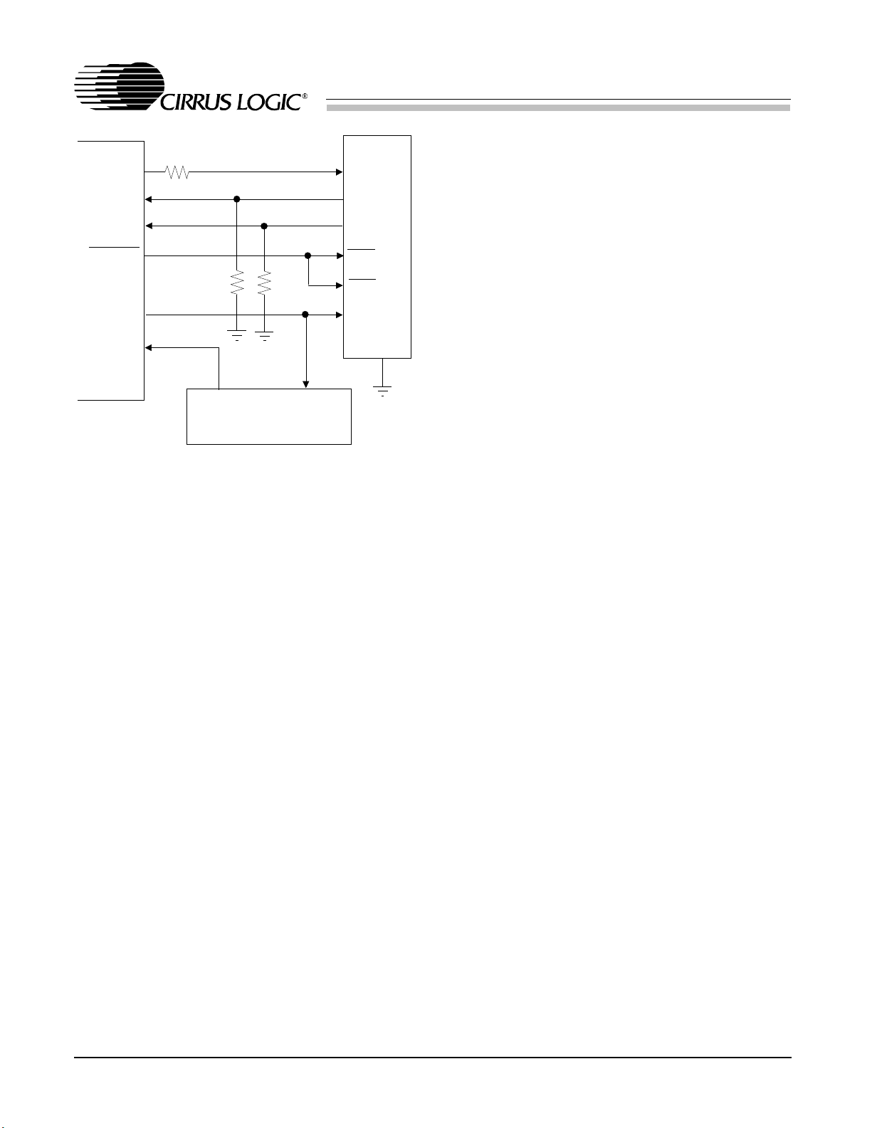
CrystalClear Low Cost ISA Audio System
TM
CS4235
Ω
100
MCLK
LRCLK
SDATA
BRESET
100k
Ω
MIDOUT
MIDIN
Joystick Connector
Figure 10. CS9236 Wavetable Serial Port Interface
100k
Midi OutMidi In
Ω
CS9236
MCLK5I
LRCLK
SOUT
RST
PDN
MIDI_IN
XTAL3I
The CS9236 data is sent to DAC2 which can be
summed into the input or output mixer. Volume
control for the serial port is supported through
I18 and I19 i n the WSS reg ister space.
The complet ion of calibration can be determin ed
by polling the Auto-Calibrate In-Progress bit in
the Error Status and Initialization register (ACI,
I11). This bit will be high whi le the cali bration is
in progress and low once completed. Transfers
enabled during calibration will not begin until
the calibration cycle has completed. Since the
part always operates at 44.1 kHz internally, all
calibration times are based on 44.1 kHz sample
periods.
The Calibratio n procedure i s as follows:
1) Place the WSS Codec in Mode Change
Enable usi ng the MCE b it of the Index Ad dress register (R0).
2) Set the CAL1,0 bits in the Interface Configuration register (I9).
3) Return fro m Mode Change Ena ble by resetting the MCE bit of the Index Addres s
register (R0).
WSS CODEC SOFTWARE DESCRIPTION
The WSS Codec must be in Mode Change Enable Mode (MCE=1) before any changes to the
Interface Configuration register (I9) or the Sample Frequency (lower four bits) in the Fs &
Playback Data Format registers (I8) are allowed.
The actual aud io data formats, which are th e upper four bits of I8 for playback and I28 for
capture, can be changed b y setting MCE (R0) or
PMCE/CMCE (I16) high. The exceptions are
CEN and PEN which can be changed "on-thefly" via programmed I/O wri tes. All outstanding
DMA transfers must be completed before new
values of CEN or PE N are recogniz ed.
Calibration
The WSS Codec has four different calibration
modes. The selected calibrat ion occurs whenever
the Mode Change Enable (MCE, R0) bit goes
form 1 to 0.
4) Wa it until 80h NOT return ed
5) Wa it until ACI (I11) cleared to proceed
NO CALIBRATION (CAL1,0 = 0 0)
This is the fastest mode since no calibration is
performed. This mode is useful for games which
require the sample frequency be changed
quickly. This mode is als o useful whe n the cod ec
is operating full-duplex and an ADC data format
change is desired. This is the only calibration
mode that does not affect the DACs (i.e. mute
the DACs). T he No Calibration mo de takes zero
sample periods.
CONVERTER CALIBRATION (CAL1,0 = 01)
This calibration mode calibrates the ADCs and
the DACs, b ut does not calibrate any o f the analog mixing channels. This is the second longest
calibration mode, taking 321 sample periods at
44.1 kHz. Because the analog mixer is not cali-
DS252PP2
67
Page 68

CrystalClear Low Cost ISA Audio System
TM
CS4235
brated in this mode, any signals fed through the
mixer will be unaffected. The calibration sequence is as fol lows:
The DACs are mut ed
The ADCs are calibrated
The DACs are cali brated
The DACs are unm uted
DAC CALIBRATION (CAL 1,0 = 10)
This calibration mode only clears the DACs
(playback) interpolation filters leaving the ADC
unaffected. This is the second fastest calibration
mode (no cal. is the fastest) taking 120 sample
periods at 44.1 kHz to co mplete. The calibra tion
sequence is as fol lows:
The DACs are mut ed
The DAC filter s are cleared
The DACs are unm uted
FULL CALIBRATION (CAL1, 0 = 11)
This calibration mode calibrates all offsets,
ADCs, DACs, and analog mixers. Full calibration will automatically be initiated on power up
or anytime the WSS Codec exits from a full
power down st ate. This is the longe st calibration
mode and takes 450 sample periods at 44.1 kHz
to complete. The calibration sequence is as follows:
All outputs are mut ed (DACs and mixer)
The mixer is calibrated
The ADCs are calibrated
The DACs are cali brated
All outputs are u nmuted
Changing Sampling Rate
The internal states of the WSS Codec are synchronized by the selected sampling frequency.
The sample freque ncy can be set in one of three
fashions. The standard WSS Code c method uses
the Fs & Playback Data Format register (I8) to
set the sampl e frequency. The changing of either
the clock source or the clock frequency divide
requires a special sequence for proper WSS
Codec operation:
1) Place the WSS Codec in Mode Change Enable using the MCE bit of the Index Addres s
register (R0).
2) During a s ingle write cycle, chang e the Clock
Frequency Divide Se lect (CFS) and/or
Clock 2 Base Select (C2SL) bits of th e Fs &
Playback Data Format register (I8) to the desired value. (The dat a format may also be
changed.)
3) The WSS Codec resynchronize s its internal
states to the new fre quency. During this time
the WSS Codec will be unable to respond.
Writes to the WSS Codec will not be recognized and reads will always retu rn the value
80 hex.
4) The host now poll s the WSS Codec’s Index
Address register (R0 ) until the v alue 80 hex
is no longer returned. On slow processor systems, 80h may go away faster than read
from software (the software would never see
it).
5) Once the WSS Code c is no longer respo nding
to reads with a va lue of 80 hex, n ormal operation can resume and the WSS Codec can
be removed from MCE.
A second method of changing the sample frequency is to di sable the sample frequency bits in
I8 (lower four b its) by setting SR E in I22. When
this bit is set, OSM1 and OSM0 in I10, along
with the rest of t he bits in I22, are used to set t he
sample frequency. Once enabled, these bits can
be changed wi thout doin g an MCE cycle.
The third method supports independent sample
frequencies (Fs) for capture and playback. The
independent sample frequency mode is enabled
by setting IFSE i n X11. Once enabled, the other
two methods for setting Fs (I8, I10, and I22) are
disabled. The capture (ADC) Fs is set in X12
and the play back (DAC) Fs is set in X13 .
68
DS252PP2
Page 69

Changing Audio Dat a Formats
In MODE 1, MCE must be used to select the
audio data format in I8. Since MCE causes a
calibration cycle, it is not ideal for full-duplex
operation. In MODE 2 and 3, individual Mode
Change Enab le bits for capture and pl ayback are
provided in register I16. MCE (R0) must still be
used to select the sample frequency, but PMCE
(playback) and CMCE (capture) allow changing
the respective data formats without causing a
calibration to occur. Setting PMCE (I16) clears
the playback FIFO and allows the upper four
bits of I8 to be changed. Setting CMCE (I16)
clears the capture FIFO and allows the upper
four bits of I28 to be changed.
Audio Data Formats
The sample frequency is always selected in the
Fs & Playback Data Format register (I8). In
MODE 1 the same register, I8, determines the
audio data format for bot h playback and capture ;
however, in MODE 2 and 3, I8 only selects the
playback dat a format and the capture data forma t
is independently selectable in the Capture Data
Format register (I28).
The WSS Codec always orders the left channel
data before the right channel. Note that these
definitions apply regardless of the specific format of the data. For example, the left sample
always comes first in the data stream regardless
of whether the sample is 16-bit or 8-bit in size.
CrystalClear Low Cost ISA Audio System
The 16-bit signed format (also called 16-bit 2’s
complement) is the standard method of representing 16-bit digital audio. This format gives
96 dB theoretical dynamic range and is the
standard for compact disk audio players. This
format uses the value -32768 (8000h) to represent maximum negative analog amplitude, 0 for
center scale, and 32767 (7FFFh) to represent
maximum positive analog amplitude.
8-BIT UNSIGNED
The 8-bit unsigned format is commonly used in
the personal computer industry. This format delivers a theoret ical dynamic range of 48 dB. This
format uses the va lue 0 (00h) to represent maximum negative analog amplitude, 128 for center
scale, and 255 (FFh) to represent maximum
positive an alog amplitude. The 16-bit signed and
8-bit unsigned transfer functions are shown in
Figure 11.
DMA Registers
The DMA registers allow easy integration of this
part into ISA systems. Peculiarities of the ISA
DMA controller require an external count
mechanism to notify the host CPU of a full
DMA buffer via interrupt. The programmable
DMA Base registers pro vide this servic e.
TM
CS4235
There are two data formats supported by the
WSS Codec: 16-bit signed (little Endian) and 8bit unsigned. See Fi gures 12-15.
16-BIT SIGNED
The 16-bit signed data format is "little Endian".
This format defines the byte orderi ng of a multibyte word as having the least significant byte
occupying th e lowest memory address. Lik ewise,
the most significant byte of a little Endian word
occupies the hi ghest memory addres s.
DS252PP2
Figure 11. Linear Transfer Functions
69
Page 70

CrystalClear Low Cost ISA Audio System
32-bit Word Time
sample 6 sam ple 5 sample 4 sample 3 sample 2 sample 1
TM
CS4235
MONO
MONOMONOMONO
0781516232431
Figure 12. 8-bit Mono, Unsigned Audio Data
32-bit Word Time
sample 3 sample 3 sample 2 sample 2 sample 1 sample 1
RIGHT
LEFTRIGHTLEFT
Figure 13. 8-bit Stereo, Unsigned Audio Data
32-bit Word Time
sample 6 sample 5 sample 4 sample 3 sample 2 sample 1
0781516232431
70
MONOMONO
0151631 2324 78
Figure 14. 16-bit Mono, Signed Little Endian Audio Data
32-bit Word Time
sample 3 sample 3 sample 2 sample 2 sample 1 sample 1
LEFTRIGHT
2324 78
Figure 15. 16-bit Stereo, Signed Little Endian Audio Data
0151631
DS252PP2
Page 71

The act of writing a value to the Upper Base
register causes both Base registers to load the
Current Count register. DMA transfers are enabled by setting the PEN/CEN bit while
PPIO/CPIO is clear. (PPIO/CPIO can only be
changed while the MCE bit is set.) Once transfers are enabled, each sample that is transferred
by a DMA cycle will decrement the Current
Count register until zero is reached. The next
sample after zero generates an interrupt and reloads the Cu rrent Count registers wi th the values
in the Base registe rs.
For all data formats the DMA Base registers
must be loaded with the number of samples, minus one, to be transferred between "DMA
Interrupts". A sample is one to four bytes wide
and is defined as all data taken at one instant in
time. Stereo and mono data contain the same
number of samples, and 8-bit data and 16-bit
data contain the same number of samples.
Symbolically:
DMA Base regist er
Where N
is the number of samples transferred
S
= NS - 1
16
between interrupts and the "DMA Base register
" consists of the concatenation of the upper
16
and lower DMA Base registers.
PLAYBACK DMA REGISTERS
The playback DMA registers (I14/15) are used
for sending playback data to the DACs in
MODE 2 and 3. In MODE 1, these registers
(I14/15) are u sed for both playback and cap ture;
therefore, full-duplex DMA operation is not possible.
CrystalClear Low Cost ISA Audio System
CAPTUR E DMA R EGIST ERS
The Capture DMA Base registers (I30/31) provide a second pair of Base registers that allow
full-duplex DMA operation. With full-duplex operation capture and playback can occur
simultaneously. These registers are provided in
MODE 2 and 3 only.
When the capture Current Count register rolls
under, the Capture Interrupt bit, CI, (I24) is set
causing the INT bit (R2) to be set. The interrupt
is cleared by a write of any value to the Status
register (R2), o r writing a "0" to the Capture Interrupt bit, CI (I24 ).
WSS Codec Interrupt
The INT bit of the Status register (R2) always
reflects the status of the WSS Codec’s internal
interrupt state. A roll-over from any Current
Count regi ster (DMA playback, DMA capture, or
Timer) sets the INT bit. This bit remains set until
cleared by a write of ANY value to Status regi ster (R2), or by clearing th e appropriate bit or bits
(PI, CI) in the Alternate Feature Status register
(I24).
The Interrupt Enable (IEN) bit in the Pin Control
register (I10) determines whether the interrupt
assigned to the WSS Codec responds to the interrupt event. When the IEN bit is low, the
interrupt is masked and the IRQ pin assigned to
the WSS Codec is held low. However, the INT
bit in the Sta tus register (R2) always respo nds to
the counter.
Error Conditions
TM
CS4235
When the playback Current Count register rolls
under, the Playback Interrupt bit, PI, (I24) is set
causing the INT bit (R2) to be set. The interrup t
is cleared by a write of any value to the Status
register (R2), or writing a "0" to the Playback
Interrupt bit, PI (I24).
DS252PP2
Data overrun or underrun could occur if data is
not supplied to or read from the WSS Codec in
an appropriate amount of time. The amount of
time for such data transfers depends on the frequency selected within the WSS Codec.
Should an overrun condition occur during data
capture, the last whole sample (before the over-
71
Page 72

CrystalClear Low Cost ISA Audio System
TM
CS4235
run condition) will be read by the DMA interface. A sample will not be overwritten while th e
DMA interface is in the process of transferring
the sample.
Should an underrun condition occur in a playback case the last valid sample will be output
(assuming DACZ = 0) to the di gital mixer. This
will mask short duration error conditions. When
the next complete sample arrives from the host
computer the data stream will resume on the
next sample clock .
The overrun and underrun erro r bits in the Alter-
nate Feature Status register, I24, are cleared by
first clearing the condition that caused the overrun or underrun error, followed by writing the
particular bit to a zero. As an example, to clear
the playback underrun bit PU, first a sample
must be sent t o the WSS C odec, and then the PU
bit must be written t o a zero.
trol pins affect the master vol ume control output
after the analog output mixer. The
UP and
DOWN pins, when low, increment and decrement the master volume. These two pins would
use SPST momentary switches. The
MUTE pin
can either be momentary or non-existent where
pressing up and down simultaneously mutes the
output volume. The circuit in Figure 16, contains
optional resistors for EMI and ESD protection;
however, the capacitors are required for switch
debounce.
UP
DOWN
MUTE
100
10 nF
Ω
Ω
100
10 nF
100
10 nF
Ω
Up
Down
Mute
GND
DIGITAL HARDWARE DESCRIPTION
The best example of hard ware connection for th e
different sections of this part is the Reference
Design Data Sheet. The Reference Design Data
Sheet contains all the schematics, layout plots
and a Bill o f Materials; ther eby providing a complete example.
Bus Interface
The ISA bus interface is capable of driving a
24mA data bus load and therefore does not require any external data bus buffering. See the
Reference Design Data Sheet for a typical connection diagram.
Volume Control In terface
Three hardware master volume control pins are
supported: volume up, volume down, and mute.
Hardware volume control is enabled by setting
the VCEN bit in the Hardware Configuration
data, byte 7 (Misc. Config. Byte). Once VCEN
is set, the XTAL1/
ACDCS/DOWN pin converts
to the volume down function. The volume con-
Figure 16. Volume Control Circuit
Pressing the up button, increments the volume.
Pressing the down button, decrements the volume. Holding either of these buttons in the low
state causes th e volume to to continue c hanging.
The formats are selected by the VCF1 bit, Hardware Configurat ion data, Glob al Config. byt e.
When VCF1 = 0, the mute funct ion is a momentary switch (similar to up and down). When
MUTE goes low the master out volume mutes if
it was un-muted and vise-versa (the mute button
alternates between mute and un-mute). If the
master volume is muted and up or down is
pressed, the vol ume automatica lly un-mutes.
When VCF1 = 1, the MUTE pin is not used.
This is a two-button format where pressing up
and down simultaneously mutes the master volume. If the master volume is muted and up or
down is individually pressed, the volume automatically un-mutes.
72
DS252PP2
Page 73

CrystalClear Low Cost ISA Audio System
TM
CS4235
The two formats listed above as illustrated in
Figure 17.
Up
Down
Mute
GND
VCF1 = 0
Figure 17. Volume Control Formats
Up
Down
Mute
GND
VCF1 = 1
Crystal / Cloc k
Tw o pins have been allocated t o allow the interfacing of a crystal oscillator: XTALI and
XTALO. The crystal should be designed as fundamental mode, parallel resonant, with a load
capacitor of between 10 and 20 pF. The capacitors connected t o each of the crystal pins should
be twice the load capacitance specified to the
crystal manufacturer.
An external CMOS clock may be connected to
the crystal input XTALI in lieu of the crystal.
When using an external CMOS clock, the
XTALO pin must be left floating with no trace
or external connec tion of any k ind.
General Purpose Output Pins
pullup resistor. VCEN has the highest precedence and will cause this pin to convert to the
DOWN function whenever VCE N is set.
Reset and Power Do wn
A RESDRV pin places the part into maximum
power conservation mode. When RESDRV goes
high, the PnP registers are reset - all logical devices are disabled, all analog outp uts are muted,
and the voltage reference then slowly decays to
ground. When RESDRV is brought low, an initialization procedure begins which causes a full
calibration cycle to occur. When initialization is
completed, the registers will contain their reset
value and the part will be isolated fr om the bus.
RESDRV is required whenever the part is powered up. The initialization time varies based on
whether an E
size of th e data in the E
2
PROM is present or not and the
2
PROM. After RESDRV
goes low, the part should not be written to for
approximately 200 ms to guarantee that the part
is ready t o respond to commands. The exact timing is spec ified in the Timing Section in t he front
of this data sheet.
Software low-power states are available through
bits in the Control or WSS logical device register space. See the CONTROL INTERFACE
section for more information.
Two ge neral purpose outputs are provided to enable control of external circuitry (i.e. mute
function). XCTL1 and XCTL0 in the WSS
Codec register I10 are output directly to the appropriate pin wh en enabled .
Pin XCTL1/
ACDCS/DOWN is initially controlled by the VCEN bit in the Hardware
Configuration data. If VCEN is zero, t his pin becomes XCTL1 if the SDOUT pin is sampled
high during a high-to-low transit ion of RESDRV.
This pin can also output
ACDCS if the SDOUT
pin is sampled low during a high-to-low transition of the RE SDRV pin. SDOUT has an int ernal
DS252PP2
Address Port Configuration
The part provides a method for motherboards to
hide the part from standard PnP (or traditional
Crystal Key) software. BIOSes can use this
method to set the part at a unique address, and
report the device as a System Dev. Node to the
operating system.
On the high to low transition of the RESDRV
pin, the pa rt samples the sta te of the APSEL and
SCL, which have internal 100 kΩ pullups to
+5 V. APSEL selects the Address Port used to
configure the p art. When APSEL is left high, the
Address Port is 0x279 and backwards compatible to previo us chips a nd standard PnP software.
73
Page 74

CrystalClear Low Cost ISA Audio System
TM
CS4235
When APSEL is externally tied to SGND, the
Address Port is moved to one of two locations,
selected by a strapping option on th e SCL pin. If
SCL is sampled high (d efault), then the Addre ss
Port is moved to 0x308. If SCL is strapped low
with an external 10 kΩ resistor to SGND, the
Address Port is moved to 0x388.
If the Address Port is moved (APSEL = 0) then
the device is no longer PnP compliant; however,
it will still respond to all the standard PnP com mands using the new Address Port. In addition,
the new Address Port supports the traditional
Crystal Key or the new Cry stal Key 2.
Multiplexed Pin Configur ation
On the high to low transition of the RESDRV
pin, the part samples the state of t he MCLK and
SDOUT which have internal 100 kΩ pullups to
+5 V.
The state of MCLK at the time RESDRV is
brought low determines the function of the
CDROM interface pins. If MCLK is sampled
high, then
CDCS, CDACK, CDINT, CDRQ are
used to input SA12, SA13, SA14, SA15 respectively. If MCLK is sampled low (external
pulldown) then
CDCS, CDACK, CDINT, C DRQ
become the standa rd CDROM interface pi ns.
The XCTL1/
ACDCS/DOWN pin state is first
determined by VCEN. If VCEN is set this pin is
forced to the
DOWN volume control pin. If
VCEN is zero, then a strapping option on
SDOUT determines the pin function. If SDOUT
is high (default) on power up, the pin is forced to
the XCTL1 general purpose output that tracks
the bit by the same name in I10 in the WSS
space. If SDOUT is externally pulled low
through a 10 kΩ resistor, then the pin is forced
to the alternate CDROM chip select function,
ACDCS.
ANALOG HARDWARE DESCRIPTION
The analog hardware consist of an MPC
Level 3-comp atible mixer. This section de scribes
the analog hardware needed to interface with
these pins.
Line-Le vel Inp uts
The analog inputs consist of three stereo analog
inputs, and one mono input. As shown in Figure 4, the input to the ADCs comes from the
Input Mixer that selects any combination of the
following: AUX1, AUX2, MIC, DAC1, DAC2,
and the output from the analog output mixer.
Unused analog inputs should be connected together and then connected through a capaci tor to
analog groun d.
The analog input interface is designed to acco mmodate two stereo inputs and two mono inputs.
Three of these sources are mixed to the ADC.
These inputs are: a mono microphone input
(MIC), a stereo CD-ROM input (AUX2), and a
stereo auxiliary line-level input (AUX1). The
MIC, AUX1, and AUX2 inputs have paths after
their volume controls, to the output mixer. The
output mixer has the additional inp ut of a mono
input chann el. All audio inpu ts should be capacitively coupled .
Since some analog inputs can be as large as
2 V
used to attenuate the analog input to 1 V
, the circuit shown in Figure 18 can be
RMS
RMS
which is the maximum voltage allowed for the
line-level i nputs.
6.8 k
Ω
6.8 k
Ω
6.8 k
Ω
Figure 18. Line Inputs
1.0 µF
1.0
6.8 k
R
µ
F
L
Ω
74
DS252PP2
Page 75

CrystalClear Low Cost ISA Audio System
TM
CS4235
The AUX2 line-level inputs have an extra pin,
CMAUX2, which provides a pseudo-differential
input for both LAUX2 and RAUX2. This pin
takes the common-mode noise out of the AUX2
inputs when connected to the ground coming
from the AUX2 analog source. Connecting the
AUX2 pins as shown in Figure 19 provides extra
noise attenuation coming from the CDROM
drive, thereby producing a higher quality signal.
Since the better the r esist ors match, t he bett er the
common-mode attenuation, one percent resistors
are recommended. If CMAUX2 is not used, it
should be connected thro ugh an AC cap to analog ground.
(All resistors 1%)
Ω
6.8 k
Ω
3.4 k
6.8 k
Ω
Ω
6.8 k
Figure 19. Differential CDROM In
3.4 k
1.0 µF
2.0 µF
Ω
1.0
6.8 k
µ
F
Ω
RAUX2
CMAUX2
LAUX2
Microphone Level Input
Ω
2 k
47 k
Ω
MC33078 or
Ω
+
MC33178
4.7 k
2.7 nF
NPO
10 µF
0.1 µF
600
Figure 20 . Mi crop hone I nput
+
Ω
1 µF
0.33 µF
X7R
47 k
Ω
VREF
MIC
MIMR bits support muting the input to the left
and right channels respectively. Figure 21 illustrates a typical input circuit for the Mono In. If
MIN is driven from a CMOS gate, the 4.7 kΩ
should be tied to AGND instead of VA+. Although this input is described for a low-quality
beeper, the input is of the same high-quality as
all other anal og inputs a nd may be used for other
purposes.
+5VA (Low Noise) or
AGND - if CMOS Source
The microphone level input, MIC, include a selectable -22.5 dB to +22.5 dB gain stage for
interfacing to an external microphone. An additional 20 dB gain block is also available. The
20 dB gain block can be switched off to provide
another mono line-level input. Figure 20 illustrates a single-ended microphone input buffer
circuit that wi ll support lowe r gain mics. The circuit in Figure 20 supports dynamic mics and
phantom-powered mics that use the ring portion
of the jack for power.
Mono Input
The mono input, MIN, is useful for mixing the
output of the "beeper" (timer chip), provided in
all PCs, with the rest of the audio signals. The
MIN pin can be mixed into the output mixer
with at a 0 or -9 dB level. Also, the MIM and
DS252PP2
4.7 k
Ω
1
47 k
Ω
0.1 µF
2.7 nF
Figure 21. Mono Input
MIN
Line Level Outputs
The analog output section provides a st ereo linelevel output. The other output types (headphone
and speaker) can be implemented with external
circuitry. LOUT and ROUT outputs should be
capacitively coupled to external circuitry. Both
LOUT and ROUT need 1000 pF NPO capacitors
between the pin and AGND.
75
Page 76

Miscellaneous Analog Signals
The VREF pin is typically 2.2 V and provides a
common mode signal for single-supply external
circuits. VREF onl y supports light DC loads and
should be b uffered if AC loading is nee ded. For
typical use, a 0. 1 µF in parallel with a 10 µF capacitor shou ld be connected to VREF.
CrystalClear Low Cost ISA Audio System
the digital ground plane to minimize coupling
into the analog section. Figure 24 s hows the recommended positioning of the decoupling
capacitors. The capacitors must be on the same
layer as, and close to, the part. The vias shown
go through to the ground and power plane layers. Vias and power supply traces should be as
large as possible to minimize the impedance.
TM
CS4235
GROUNDING AND LAYOUT
Figure 22 is a suggested layout for motherboard
designs and Figure 23 is a suggested layout for
add-inn cards. For optimum noise performance,
the device should be located across a split analog/digital ground plane. The digital ground
plane should extend across the ISA bus pins as
well as the internal digital interface pins.
DGND1 is ground for the data bus and should
be electrically connected to the digital ground
plane which will mini mize the effects of the bus
interface due to transient currents during bus
switching. SGND1-4 sh ould also be c onnected to
POWER SUPP LIES
The power supply providing analog power
should be as clean as possible t o minimize coupling into the analog section and degrading
analog perf ormance.
The VD1 is isolated from the rest of the power
supply pins and provide digital power for the
asynchronous parallel ISA bus. The VD1 pin can
be connecte d directly to the system di gital power
supply.
Di
g
i
t
a
l
G
r
o
Crystal
Part
u
n
d
N
o
ise
Analog
Ground
1
76
Digital
Ground
Figure 22. Suggested Motherboard Layout
Digital Ground Noise
o
r
G
l
a
t
i
g
i
D
N
d
n
u
e
s
i
o
Power
Connector
DS252PP2
Page 77

CrystalClear Low Cost ISA Audio System
TM
CS4235
PIN 1
PIN 98
VDF3
Speaker Out
CD-ROM
Speaker In
Analog Ground
1
Digital Ground
Figure 23. Suggested Add-In Card Layout
1
PIN 80
PIN 97
.1
µ
F
SGND3
PIN 81
VA
AGND
.1
µ
F
µ
.1
Crystal
Part
F
+
PIN 79
REFFLT
F
µ
PIN 17
VDF1
.1
µ
F
PIN 18
SGND1
Analog
Digital
vias through to
=
power/ground plane
PIN 45
VD1
Figure 24. Recommended Decoupling Capacitor Positions
PIN 46
DGND1
.1
F
µ
PIN 71
TEST
PIN 66
SGND2
PIN 65
VDF2
PIN 53
SGND4
µ
F
.1
DS252PP2
77
Page 78

VDF1 through VDF3 provide power to internal
digital sections of the codec and should be quieter than VD1. This can be achieved by using a
ferrite bead to the VD1 su pply.
VA provides power to the sensitive analog sections of the chip and should have a clean,
regulated supp ly to minimize power supply coupled noise i n the analo g inputs and o utputs.
ADC/DAC FILTER RESPONSE PL OTS
Figures 25 through 30 show the overall frequency response, passband ripple, and transition
band for the ADCs an d DACs. Figure 31 shows
the DACs’ deviation from linear pha se. Since th e
filter response scales ba sed on sample frequency
selected, all frequency response plots x-axis are
shown from 0 to 1, where 1 is equivalent to Fs.
Therefore, for any gi ven sample frequency, multiply the x-axis values by the sample frequency
selected to get the actual frequency.
CrystalClear Low Cost ISA Audio System
10
0
-
10
-
20
-
30
-
40
-
50
-
60
Magnitude (dB)
-
70
-
80
-
90
-
100
0
.
00.10.20.30.40.50.60.70.80.91.0
TM
Input Freque nc y ( x Fs)
CS4235
0.2
0.
1
0
.
0
-0.
1
-0.
2
3
-0.
-0.
4
Magnitude (dB)
-0.
5
-0.
6
-0.
7
-0.
8
0
.
00 0.05 0.10 0.15 0.20 0.25 0.30 0.350.40 0.45 0.50
Input Frequency ( x Fs)
Figure 26. ADC Passband Ripple
78
Figure 25. ADC Filter Response
0
1
0
2
0
3
0
4
0
-
5
0
-
-60
Magnitude (dB)
7
0
-
-80
9
0
-
10
0
-
0.40 0.45 0.50 0.55 0.60 0.65 0.70
Input Frequency ( x Fs)
Figure 27. ADC Transition Band
DS252PP2
Page 79
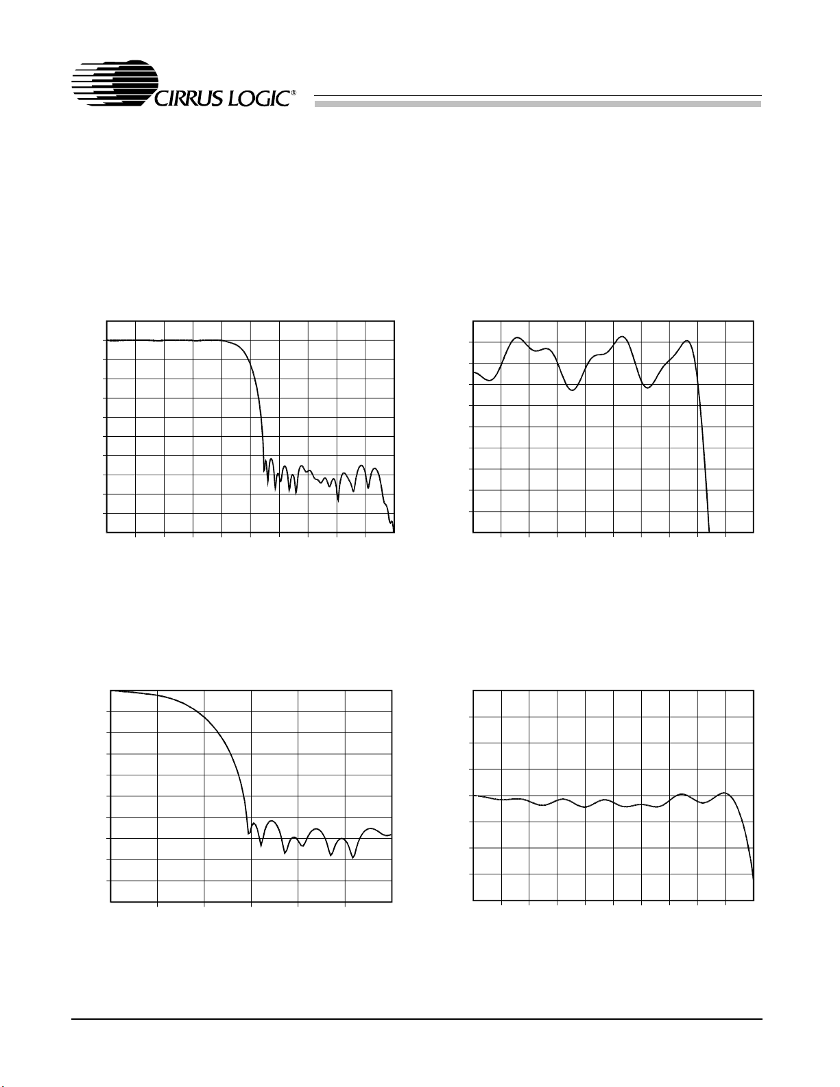
CrystalClear Low Cost ISA Audio System
TM
CS4235
10
0
-
10
-
20
-
30
-
40
-
50
-
60
Magnitude (dB)
-
70
-
80
-
90
-
100
0
.
00.10.20.30.40.50.60.70.80.91.0
Input Frequency ( x Fs)
Figure 28. DAC Filter Response
0
-
10
-
20
-
30
-
40
50
-
-
60
Magnitude (dB)
70
-
-
80
-
90
-
100
0.40 0.45 0.50
Input Frequency ( x Fs)
0.55 0.60 0.65 0.70
0.2
.
1
0
.
0
0
-0.
1
-0.
2
-0.
3
-0.
4
Magnitude (dB)
-0.
5
-0.
6
-0.
7
-0.
8
0
.
00 0.05 0.10 0.15 0.200.25 0.300.35 0.400.45 0.50
Input Frequency ( x Fs)
Figure 29. DAC Passband Ripple
2.0
1
.
5
1
.
0
0
.
5
0.0
-0.
5
Phase (degrees)
∆
-1.
0
-1.
5
-2.
0
.
00 0.05 0.10 0.150.20 0.250.30 0.350.40 0.45 0.50
0
Input Frequency ( x Fs)
DS252PP2
Figure 30. DAC Transition Band
Figure 31. Deviation from Linear Phase
79
Page 80

PIN DESCRIPTIONS
CS4235
82
81
TM
T
L
D
F
F
N
F
G
E
A
A
V
R
79
80
78
I
O
E
T
T
R
L
L
F
V
F
76
77
CrystalClear Low Cost ISA Audio System
K
T
S
C
D
2
C
X
99
3
O
3
L
F
A
D
T
V
X
97
98
I
L
A
T
X
100
/
*
U
E
D
2
T
A
N
1
U
M
G
A
M
C
S
S
94
95
96
C
A
D
C
/
*
3
1
A
93
Q
N
I
R
D
D
V
C
C
/
*
4
1
A
S
S
92
91
L
R
/
*
D
5
S
1
E
A
R
S
90
89
D
E
3
S
T
N
I
P
L
A
M
F
87
88
86
85
2
2
X
X
U
U
C
I
A
A
R
M
L
83
84
SDATA
LRCLK
MCLK
FSYNC
SDOUT
SDIN
SCLK
SDA
UP
XCTL0
SCL
BRESET
XCTL1*/ACDCS/DOWN
VDF1
SGND1
(INT15*) IRQF
(INT12*) IRQE
(INT11*) IRQD
(INT9*) IRQC
(INT7*) IRQB
(INT5*) IRQA
SA0
10
11
12
3
4
5
6
7
8
9
13
14
15
16
22
23
1
2
17
18
19
20
21
24
25
(TOP VIEW)
28
26
27
3031323334
29
TQFP
100-PIN
35
36
CS4235
37
383940
41
42
434445
46
47
48
49
50
59
56
55
54
53
52
51
LAUX1
75
74
RAUX1
73
LOUT
72
R
71
70
69
68
67
66
65
64
63
62
61
60
58
57
O
TEST
JAB1
JBB1
JACX
JBCX
SGND2
VDF2
JBCY
JACY
JBB2
JAB2
MIDOUT
MIDIN
DACKA (DACK0*)
DACKC (DACK3*)
DACKB (DACK1*)
DRQA (DRQ0*)
IRQG (INT10)
SGND4
DRQC (DRQ3*)
DRQB (DRQ1*)
U
T
6
7
1
3
2
4
5
6
A
S
A
A
A
S
A
A
S
S
S
S
0
7
8
9
R
1
A
A
A
O
I
A
S
S
S
S
IOW
SA11
0
Y
N
D
E
D
S
A
R
H
C
O
I
3
1
2
1
D
S
D
D
D
V
S
S
5
4
1
D
N
G
D
D
D
D
D
S
S
S
S
* Defaults - See i ndividual pin descri ptions for more details
80 DS252PP2
Page 81

ISA Bus Interface Pins
SA<11:0 > - System Address Bus, Inputs
These signals are decoded during I/O cycles to determine access to the various functional
blocks within the part as defined by the configuration data written during a Plug and Play
configuration sequence.
SA<15:12> - Upper System Address Bus, Inputs
These signals are multi-function pins, shared with the CDROM, that default to the upper
address bits SA12 through SA15. These pins are generally used for motherboard designs that
want to eliminat e address decode ali asing. Using the se pins as upper address bits forces the part
to only acc ept valid address de codes when A12-A15 = 0. If these pins are not used for address
decodes or for CDROM support, they should be tied to SGND. These pins are forced to the
CDROM interface when a 10 kΩ resistor is placed on pin MCLK to SGND.
SD<7:0> - System Data Bus, Bi-directional, 24 mA drive
These signal s are used to transfer data to and f rom the p art.
CrystalClear Low Cost ISA Audio System
TM
CS4235
AEN - Address Enable, Input
This signal i ndicates whether t he current bus c ycle is an I/O cycle or a DMA cycle . This signal
is low during an I/O c ycle and hi gh during a DMA cycle.
IOR - Read Command Strobe, Input
This active low signal defines a read cycle to the part. The cycle may be a register read or a
read from the part’s DMA registers.
IOW - Write Command Strobe, Input
This active low signal indicate s a write cycle to the pa rt. The cycle may be a write to a control
register or a DMA register.
IOCHRDY - I/O Channel Ready, Open Drain Output, 8 mA drive
This signal is driven low by the part during ISA bus cycles in which the part is not able to
respond within a minimum cycle time. IOCHRDY is forced low to extend the current bus
cycle. The bus cycle is ext ended unti l IOCHRDY is brought high.
DRQ<A,B,C> - DMA Requests, Outputs, 24 mA drive
These active h igh outputs are ge nerated when the part is requesting a DMA transfer. This signal
remains high until all the bytes have been transferred as defined by the current transfer data
type. The DRQ<A, B,C> outputs mus t be connected to 8 -bit DMA ch annel request signals only.
The defaults on the ISA bus are DRQA = DRQ0, DRQB = DRQ1, and DRQC = DRQ3. The
defaults can be c hanged by mod ifying the Hardware Resource data .
DS252PP2 81
Page 82

DACK<A,B,C> - DMA Acknowl edge, Inputs
The assertion of these active low signals indicate that the current DMA request is being
acknowledged and the part will respond by either latching the data present on the data bus
(write) or putting data on the bus (read). The
DACK<A,B,C> input s must be connected to 8-bit
DMA channel acknowledge lines only. The defaults on the ISA bus are
DACKB = DACK1, and DACKC = DACK3. The defaults can be changed by modifying the
Hardware Resource data.
IRQ <A:G>- Host Interrupt Pins, Outputs, 24 mA drive
These sign als are used to notify the host o f events which n eed servicin g. They are connected to
specific interrupt lines on the ISA bus. The IRQ<A:G> are individually enabled as per
configuration data that i s generated duri ng a Plug and Play configu ration sequen ce. The defau lts
on the ISA bus are IRQA = INT5, IRQB = INT7, IRQC = INT9, IRQD = INT11,
IRQE = INT12, IRQF = INT15. IRQG is new to the CS4235 and defaults to unconnected for
compatibility reasons. For new designs, IRQG is typically connected to IRQ10. The defaults
can be changed by modifying the Hardware Configurat ion data lo aded from the E
RESDRV - Reset Drive, Input
Places the part in l owest power consumption mode. All sections of the part are shut down and
consuming minimal power. The part is reset and in power down mode when this pin is logic
high. Th e falling edge also latch es the state of MC LK and SCLK t o determine the functionalit y
of dual mode pins , and SCL to determin e the Address Po rt. This sig nal is typi cally conn ected to
the ISA bus signal RESDRV. RESDRV must be asserted whenever the part is powered up to
initialize the internal registers to a known state. Th is pin, when high, also drives the
pin low.
CrystalClear Low Cost ISA Audio System
TM
DACKA = DACK0,
2
PROM.
BRESET
CS4235
Analog Inputs
MIC - Mic Input
Microphone input c entered around VREF. A programmable gain block provides volume contro l
and is located i n X2 with mutes located in X2 an d X3.
LAUX1 - Left Auxiliary #1 Input
Nominally 1 V
max analog input for the Left AUX1 channel, centered around VREF. A
RMS
programmable gain block provides volume control and is located in I2. Typically used for an
external Left lin e-level inp ut.
RAUX1 - Right Auxiliary #1 Input
Nominally 1 V
max analog input for the Right AUX1 channel, centered around VREF. A
RMS
programmable gain block provides volume control and is located in I3. Typically used for an
external Righ t line-level in put.
82 DS252PP2
Page 83

LAUX2 - Left Auxiliary #2 Input
Nominally 1 V
max analog input for the Left AUX2 channel, centered around VREF. A
RMS
programmable gain block provides volume control and is located in I4. Typically used for the
Left channel CDROM i nput.
RAUX2 - Right Auxiliary #2 Input
Nominally 1 V
max analog in put for the Right AUX2 cha nnel, centered around VR EF. A
RMS
programmable gain block provides volume control and is located in I5. Typically used for the
Right channel CDR OM input.
CMAUX2 - Common Mode Auxiliary #2 Input
Common mode ground input for the LAUX2 and RAUX2 inputs. Typically connected to the
CDROM ground input to provide common-mode noise rejection. The impedance on this pin
should be one half th e impedance o n the LAUX2 and RAUX2 inputs.
MIN - Mono Input
Nominally 1 V
max analog input, centered around VREF, that goes through a
RMS
programmable gai n stage (I2 6) into both channels of the outpu t mixer. This is a general purp ose
mono analog input that is no rmally used to mix the typical "beeper" signal o n most computers
into the audi o system.
CrystalClear Low Cost ISA Audio System
TM
CS4235
REFFLT - Reference Filter, Input
Voltage reference used internal to the part . A 0.1 µF and a 1 µF capac itor with short fat traces
must be conne cted between this pin a nd AGND. No other connection s should be made to this
pin.
Analog Outputs
LOUT - Left Line Level Output
Analog output from the mixer for the left channel. Nominally 1 V
VREF. A 1000 pF NPO cap acitor must be at tached from t his pin to AGND.
ROUT - Right Line Level Output
Analog output from the mixer for the Right chan nel. Nominally 1 V
VREF. A 1000 pF NPO cap acitor must be at tached from t his pin to AGND.
FLT3D - 3D Filter
A 0.01 µF capacitor must be at tached from this pin to AGND.
FLTO - Filter Output
A 1000 pF NPO cap acitor must b e attached between thi s pin and FLTI.
max centered around
RMS
max centered ar ound
RMS
DS252PP2 83
Page 84

FLTI - Filter Input
A 1000 pF NPO cap acitor must b e attached between thi s pin and FLTO.
VREF - Voltage Reference, Output
All analog inputs and outputs are centered around VREF which is nominally 2.1 Volts. This
pin may be used to le vel shift externa l circuitry, although any AC loads should be buffered.
MIDI Interfa ce
MIDOUT - MIDI Out Transmit Data, Output, 4 mA drive
This output is used to send MIDI data serially out to a external MIDI device. Normally
connected to pin 12 of the joy stick connec tor for use with bre akout boxes.
MIDIN - MIDI In Receive Data, Input - Internal Pullup
This input i s used to rece ive serial MIDI data from an ext ernal MIDI device. This pin shou ld be
connected to pin 15 of the joy stick connec tor for use with bre akout boxes.
CrystalClear Low Cost ISA Audio System
TM
CS4235
External Peripher al Signals
SDA - E
2
PROM Data Pin, Bi-directional, Open Drain, 4 mA sink
This open-drain pin must have an ext ernal pullup (3.3 kΩ) and is used in conjunction with SCL
2
PROM. When an E2PROM is used, the SDA pin should be
2
PROM device and provides a bi-directional data port. The
SCL - E
to access an external serial E
connected to the data pin of the E
2
E
PROM is used to set the Pl ug and Play reso urce data.
2
PROM Serial Clock, Output, 4 mA drive (Address Port Selection)
When E
output to the E
2
PROM access is enabled, via EEN in CTRLbase+1, then SCL is used as a clock
2
PROM. At power-up, th is pin is an inp ut (with an intern al 100 kΩ pullup) tha t
selects between two alternate addresses for the Address Port used to configure the chip.
Assuming APSEL is strapped low, SCL hig h selects 308h a s the Address Port, and when SCL is
tied low (with a 1 0 kΩ resistor to ground), the Address Port is 388h.
XCTL0 - External Control, Output, 4 mA drive
This pin is a general purpose out put pin controlled by t he XCTL0 bit in the WSS register I10.
BRESET - Buffered Reset, Output, 4 mA drive
This active low signal goes low wh enever the RESDRV pin goes high. This pin is also software
controllable through the BRES bit in register C8 in the Control Logical Device space. BRES
provides a so ftware power down and reset control over d evices connected to the CS42 35 such
as the CS9236 Singl e-Chip Wavetable Music Synth esizer.
84 DS252PP2
Page 85

CrystalClear Low Cost ISA Audio System
Joystick Inter face
JACX, JACY - Joystick A Coordinates, Input
These pins are the X/Y coordinates for Joystick A. They should have a 5.6 nF capacitor to
ground and a 2. 2 kΩ resistor to the joystic k connecto r pins 3 and 6, respectiv ely.
JAB1, JAB2 - Joystick A Butto ns, Input - Internal Pullups
These pins are the switch input s for Joy stick A. They shou ld be con nected to jo ystick conn ector
pins 2 and 7, resp ectively; a s well as have a 1 nF capacitor to gro und.
JBCX, JBCY - Joystick B Coordinates, Input - Internal Pullups
These pins are the X/Y coordinates for the second joystick, Joystick B. They should have a
5.6 nF capacitor to ground and a 2.2 kΩ resistor to the joystick connector pins 11 and 13,
respectively.
JBB1, JBB2 - Joystick B Buttons, Input
These pins are the s witch inputs for the second joystick, Joystick B. They should be conne cted
to joystick con nector pins 10 and 14, respe ctively; as we ll as have a 1 nF cap acitor to gro und.
TM
CS4235
CS4610 DSP Serial Port Interface
FSYNC - Frame Sync, Output, 4 mA drive
When the serial port is enabled, SPE = 1 in I16, this pin is the serial frame sync output .
SCLK - Serial Clock, Output, 4 mA drive
When the serial port is enabled, SPE = 1 in I16, th is pin is the serial clock outp ut.
SDOUT - Serial Data Output, Output, 4 mA drive (Alternate CDROM Chip Select Enable)
When the serial port is enabled, SPE = 1 in I16, this pin is the se rial data output. At po wer-up,
this pin is an input (with an internal 100 kΩ pullup) that, when pulled low with a 10 kΩ
resistor to SGND, enables the alternate CDROM chip select pin
ACDCS. Loading must be
limited to CMOS inp uts if this pi n has the 10 kΩ re sistor at tached .
SDIN - Serial Data Input, Input
When the serial port is enabled, SPE = 1 in I16, th is pin is the serial data input .
CS9236 Wavetab le Seri al Port Inte rface
A digital interface to the CS9236 Single-Chip Wavetable Music Synthesizer is provided that
allows the CS9236 PCM audio data to be summed on the CS4235 without the need for an
external DAC. This serial port is enabled via the WTEN bit which is located in the Global
Configuration byte in the E
2
PROM Hardware Configuration data, or C8.
DS252PP2 85
Page 86

CrystalClear Low Cost ISA Audio System
SDATA - Wave table Serial Audio Data , Input
This input sup plies the serial aud io PCM data to be mixed to the stereo DAC2 of the CS4235.
The data consist s of left and righ t channel 1 6-bit data deli neated by LRC LK. This pin shou ld be
connected to t he SOUT output pin on the CS9236. This pi n should also ha ve a weak pull-down
resistor of approx . 100 kΩ to min imize power-down currents and allow for stuffing options .
LRCLK - Wavetable Serial Left/Right Clock, Input
This input sup plies the serial data alignment sign al that delineates l eft from right data. T his pin
should be connected to the LRCLK output pin on the CS9236. This pin should also have a
weak pull-down resistor of approx. 100 kΩ to minimize power-down currents and allow for
stuffing options.
MCLK - Wav etable Master Clock, Output (CDROM enable)
This output supp lies the 16.9344 MHz mas ter clock that control s all the timing on the CS9236.
This pin shoul d be connect ed to the MCLK5I input pin on the CS9236. MCLK c an be disabled
in software usi ng the DMCLK bit in C8 in the Control l ogical device spa ce. DMCLK provides
a partial softwa re power-down mode for th e CS9236. At p ower-up, this pin is an input (with an
internal 100 kΩ pullup) that, when pulled low with a 10 kΩ resistor to SGND, enables the
CDROM interface (over the upper four ISA address pins).
TM
CS4235
CDROM Interface
The four CDROM pins are multi-function and default to ISA upper address bits SA12-SA15.
To enable the CDROM port, an external 10 kΩ resistor must be tied between MCLK and
SGND. MCLK is sampled on the falling edge of RE SDRV. The alternate CDROM chip select
has its own strapping option to enable
2
E
PROM to support the Plug-and-Play dat a as well as firmware pat ch data.
ACDCS. Use of the CDROM interface requires a 1 k
CDCS - CDROM Chip Select, Output, 4 mA drive
This output g oes low whenever an addre ss is decoded that match es the value programmed int o
the CDROM base address register.
ACDCS - Alternate CDROM Chip Select, Output, 4 mA driv e
This pin, XCTL1 /
ACDCS/DOWN, is multiplex ed with two other functions, and defaults to the
XCTL1 output which is controlled by the XCTL1 bit in the WSS I10. This pin can also be
configured at a second CDROM Chip Select,
ACDCS, to support the alternate IDE CDROM
decode. To force this pin to the CDROM alternate c hip select, an exte rnal 10 kΩ resistor must
be tied between SDOUT and SGND.
ACDCS output then goes low whenever an address is
decoded that matches the value programmed into the CDROM alternate base address register,
ACDbase. This pin can also be used as the volume up pin
register C0 or the Hardware Configuration data. VCEN has the highest precedence over the
other pin function s.
DOWN by setting VCEN in Control
86 DS252PP2
Page 87

CrystalClear Low Cost ISA Audio System
CDINT - CDROM Interrupt, Input
This pin is used to input an interrupt signal from the CDROM interface. The part can be
programmed, through the plug-and-play resource data, to output this signal to the appropriate
ISA bus interrupt line. The polarity if this input can be programmed through CTRLbase+1
register, bit ICH, or the Hardware Configurati on data; the de fault is activ e high.
CDRQ - CDROM DMA Request, Input
This pin can be used to in put the DMA request signal from the CDROM interface. The part can
be programmed, through the plug-and-play resource data, to output this signal to the
appropriate I SA bus DRQ line.
CDACK- CDROM DMA Acknowledge, Output, 4 mA drive
This pin c an be used to outpu t the ISA bus-generated DMA acknowledge signal to the C DROM
interface.
Volume Contr ol
The volume control pins are enabled by setting VCEN in the Hardware Configuration data,
Misc. Hardware Config. byte. The VCF1 bit in the Hardware Configuration data, Global
Configuration byte, set th e format for the vo lume control p ins. Ty pically a 100 Ω series resi stor
and a 10 nF capacitor (required) to ground, capacitor on the switch side of the series resistor,
would be included on each pin for ESD protection and to help with EMI emissions.
TM
CS4235
UP - Volume Up, Input - Internal Pullup
This pin is enabled when VCEN is set. When
incremented. A 10 nF capacitor to ground is requ ired for switch deboun ce.
DOWN - Volume Down, Input - Internal Pullup
The XCTL1/
ACDCS/DOWN is a multiplexed pin that can be used as XCTL1, the alternate
CDROM chip select, or the Volume Down pin. This pin is switched to the
when VCEN is set. When
DOWN is low, the master volume output is decremented. A 10 nF
capacitor to gr ound is require d for switch debo unce.
MUTE - Volume Mute, Input - Internal Pullup
The
MUTE pin function ca n be momentary, or non-existent based on the VCF1 bit. The MUTE
function is enabled when VCEN is set. A 10 nF capacitor to ground is required for switch
debounce.
Miscellaneous
XTALI - Crystal Input
This pin will accept either a crystal, with the other pin attached to XTALO, or an external
CMOS clock. XTAL must have a crystal or clock source attached for proper operation. The
crystal frequency mus t be 16.9344 MHz and designed for fundament al mode, parallel resonanc e
operation.
UP is low, the master volume output is
DOWN function
DS252PP2 87
Page 88

XTALO - Crystal Output
This pin is u sed for a crystal placed between this pin and XTALI. If an external clock is u sed
on XTALI, this pin must be le ft floating with n o traces or compon ents connect ed to it.
APSEL - Address Port Select, Input
This pin has an internal pull-up of approximately 100 kΩ. Leaving this pin in its default
condition, p laces the PnP/Crystal Key Address Port at the standard PnP address of 279h (hex).
For Motherboard applications, APSEL can be tied to SGND, which will change the Address
Port to one of two other add resses, chosen by a strapping option on pin SCL . When RESDRV
goes inactiv e, pin SCL is forced to an input and sampled. Whe n SCL is sampled high (defau lt),
the Address Port ch anges to addre ss 308h. When SCL is sampled low, the Address Port changes
to 388h. Add-i n cards shoul d leave APSEL unconnected
TEST - Test
This pin must be tied to ground for prop er operation.
Power Supplies
CrystalClear Low Cost ISA Audio System
TM
CS4235
VA - Analog Supply Voltage
Supply to the a nalog section of t he codec.
AGND - Analog Ground
Ground reference to the analog section of the codec. This pin should be placed on an analog
ground pin separate fro m other chip gro unds.
VD1 - ISA Dig ital Supply Voltage
Digital supply fo r the ISA parallel data bus pins.
DGND1 - ISA Digita l Ground
Digital ground reference for the ISA parallel data bus pins. These pins are isolated from the
other grounds and should be connected to the digital ground section of the board (see
Figure 24).
VDF1, VDF2, VDF3 - Digita l Filtered Supply Vo ltage
Digital supply for the internal digital section of the codec (except for the parallel data bus).
These pins should be filtered, using a ferrite bead, from VD1.
SGND1, SGND2, SGND3, SGND4 - Internal Digital Grounds
Ground reference for the internal digital portion of the codec. Optimum layout is achieved by
placing SGND1/2/3/4 on the digi tal ground plan e with the DGND pin as shown in Figure 24.
88 DS252PP2
Page 89

PARAMETER DEFINITIONS
Frequency Response
Frequency Response is the deviation in signal l evel verses freq uency. The 0 dB reference p oint
is 1 kHz. Th e amplitude co rner, Ac, lists the maximu m deviation in amplitude abov e and below
the 1 kHz reference point. The listed minimum and maximum fre quencies are guaranteed t o be
within the Ac from mi nimum frequenc y to maximum freq uency inclusiv e.
Total Dynamic Range
TDR is the ratio of the RMS sum of the lowest obtainable noise floor, in the presence of a
signal, divi ded by the RMS full-scale si gnal level. The lowest obtain able noise floor is define d
as the noise flo or measured with th e attenuation bit s for the volume contro l at full attenuation without muting. Mea sured over a 20 Hz to 2 0 kHz bandwidth with u nits in dB FS A. (dB FS is
defined as d B relativ e to full-scal e. The "A" in dicates an A weighting filte r was used. )
Instantaneous Dynamic Range or Dynamic Range
IDR or DR is the ratio of the RMS sum of the nois e floor, in the pres ence of a signal, divided
by the RMS full-scale signal le vel, available at an y instant in time (n o change in gain setti ngs
between measurements). Measured over a 20 Hz to 20 kHz band width with units in dB FS A.
(dB FS is defined as dB relative to full-scale. The "A" indicates an A weighting filter was
used.)
CrystalClear Low Cost ISA Audio System
TM
CS4235
Total Harmonic Distorti on plus Noise
THD+N is the ratio of th e RMS sum of all non-fundamental frequency components, div ided by
the RMS ful l-scale si gnal lev el. Tested using a -3 dB FS in put signa l. Measure d over a 20 Hz t o
20 kHz bandwidth with units in dB FS A. (dB FS is defined as dB relative to full-scale. The
"A" indicates an A weighting filter was used.)
Interchannel Isolation
The ratio of signal le vel on the tested channel divided by the stimu lus channel level. For input s,
the tested input channel is terminated with 50 Ω. For outpu ts, the tested channel is fed digital
zeros. Units in dB.
Interchannel Gain Mismatch
For the ADCs, the difference in input voltage to get an equal code on both channels. For the
DACs, the difference in output voltages fo r each channel when both channels are fed the same
code. Units in d B.
PATHS:
A-D-PC: Analog in, thro ugh ADC, onto PC bus
PC-D-A: PC bus, throug h DAC, to analog out
A-A: Analog in to An alog ou t (analog ou tput mixe r)
Detailed information on audio testing and paths can be found in Personal Computer Audio Quality
Measurements doc ument by Dr. Steven Harris and Cl if Sanchez, locate d at the followin g web addres s:
http://www.cirrus.c om/products/papers/mea s/meas.html.
DS252PP2 89
Page 90

PACKAGE PARAMETERS
D
D1
E
E1
CrystalClear Low Cost ISA Audio System
TM
100-pin TQFP - Packag e Co de ’Q’
Symbol Description
N
A
A1
b
c
D
D1
E
E1
e1
L1
T
Lead Co unt
Overall Height
Stand Off
Lead Width
Lead Thickness
Terminal Dim e ns ion
Package Body
Terminal Dim e ns ion
Package Body
Lead Pitch
Foot Length
Lead Angle
MIN NOM MAX
100
0.00
0.14
0.077
15.70
0.20
0.127
16.00
14.0
15.70
16.00
14.0
0.40
0.30
0.50
0.50
0.0° 12.0°
CS4235
1.66
0.26
0.177
16.30
16.30
0.60
0.70
Notes:
1) Dimensions in millimeters.
100
1
L1
e1 b
T
A1
A
2) Package body dimensions do not include mold protrusion,
which is 0.25 mm.
3) Coplanarity is 0.004 in.
4) Lead frame material is AL-42 or copper, and lead finish
is solder plate.
5) Pin 1 identification may be either ink dot or dimple.
6) Package top dimensions can be smaller than bottom
dimensions by 0.20 mm.
7) The "lead width with plating" dimension does not include
a total allowable dambar protrusion of 0.08 mm (at
maximum material condition ).
c
8) Ejector pin marks in molding are present on every package.
90 DS252PP2
Page 91

CrystalClear Low Cost ISA Audio System
APPENDIX A: DEFAULT PnP DATA
; EEPROM Vali dation Bytes
DB 055H, 0BBH ; EEPROM Validation Byte s: CS4235
DB 001H ; EEPR OM data length upper byte
DB 014H ; lowe r byte, Listed Size = 276
; Hardware Co nfiguration Data
DB 000H ; ACDb ase Addr. Mask Length = 1 b ytes
DB 003H ;
DB 080H ; MCB: IHCD
DB 080H ; GCB1: IFM
DB 005H ; Code Base Byte
DB 020H ; FM Scaling 0 dB
DB 004H ; RESERVED
DB 008H ; RESERVED
DB 010H ; RESERVED
DB 080H ; M+DSP: MIM
DB 000H ;
DB 000H ; GCB2: No Bits Set
TM
CS4235
; Hardware Ma pping Data
DB 004H ; CDbase Length = 4
DB 048H ; RESERVED
DB 075H ; IRQ s election A & B - B= 7, A=5
DB 0B9H ; IRQ s election C & D - D=11, C=9
DB 0FCH ; IRQ s election E & F - F=15, E=12
DB 010H ; DMA s election A & B - B= 1, A=0
DB 003H ; DMA C ,IRQ G select. - G= 0, C=3
; PnP Resourc e Header - PnP ID for CS423 6 IC, OEM ID = 42
DB 00EH, 063H , 042H, 036H, 0FFH,0FFH, 0FFH,0FFH,0A9H ; CSC 4236 FFFFFFFF
DB 00AH, 010H , 005H ; PnP version 1.0, V endor version 0.5
DB 082H, 00EH , 000H, ’Crystal Codec’, 000H ; ANSI ID
; LOGICAL DEV ICE 0 (Windows Sound Syst em & SBPro)
DB 015H, 00EH , 063H, 000H, 000H, 000H ; EISA ID: CSC0000
DB 082H, 007H , 000H, ’WSS/SB’, 000H ; A NSI ID
DB 031H, 000H ; DF Best Choice
DB 02AH, 002H , 028H ; DMA: 1 - WSS & SBPro
DB 02AH, 009H , 028H ; DMA: 0,3 - WSS & SBP ro capture
DB 022H, 020H , 000H ; IRQ: 5 Interrupt S elect 0
DB 047H, 001H , 034H, 005H, 034H, 005H, 004H, 004H ;16b WSSba se: 534
DB 047H, 001H , 088H, 003H, 088H, 003H, 008H, 004H ;16b SYNba se: 388
DB 047H, 001H , 020H, 002H, 020H, 002H, 020H, 010H ;16b SBbas e: 220
DB 031H, 001H ; DF Acceptable Choice 1
DB 02AH, 00AH , 028H ; DMA: 1,3 - WSS & SBP ro
DB 02AH, 00BH , 028H ; DMA: 0,1,3 - WSS & S BPro capture
DB 022H, 0A0H , 09AH ; IRQ: 5,7,9,11,12 ,15 Interrupt Select 0
DS252PP2 91
Page 92

CrystalClear Low Cost ISA Audio System
DB 047H, 001H , 034H, 005H, 0FCH, 00FH, 004H, 004H ;16b WSSba se: 534-FFC
DB 047H, 001H , 088H, 003H, 088H, 003H, 008H, 004H ;16b SYNba se: 388
DB 047H, 001H , 020H, 002H, 060H, 002H, 020H, 010H ;16b SBbas e: 220-260
DB 031H, 002H ; DF Suboptimal Choice 1
DB 02AH, 00BH , 028H ; DMA: 0,1,3 - WSS & S BPro
DB 022H, 0A0H , 09AH ; IRQ: 5,7,9,11,12 ,15 Interrupt Select 0
DB 047H, 001H , 034H, 005H, 0FCH, 00FH, 004H, 004H ;16b WSSba se: 534-FFC
DB 047H, 001H , 088H, 003H, 0F8H, 003H, 008H, 004H ;16b SYNba se: 388-3F8
DB 047H, 001H , 020H, 002H, 000H, 003H, 020H, 010H ;16b SBbas e: 220-300
DB 038H ; End o f DF for Logical Device 0
; LOGICAL DEV ICE 1 (Game Port)
DB 015H, 00EH , 063H, 000H, 001H, 000H ; EISA ID: CSC0001
DB 082H, 005H , 000H, ’GAME’, 000H ; ANS I ID
DB 031H, 000H ; DF Best Choice
DB 047H, 001H , 000H, 002H, 000H, 002H, 008H, 008H ;16b GAMEb ase: 200
TM
CS4235
DB 031H, 001H ; DF Acceptable Choice 1
DB 047H, 001H , 008H, 002H, 008H, 002H, 008H, 008H ;16b GAMEb ase: 208
DB 038H ; End o f DF for Logical Device 1
; LOGICAL DEV ICE 2 (Control)
DB 015H, 00EH , 063H, 000H, 010H, 000H ; EISA ID: CSC0010
DB 082H, 005H , 000H, ’CTRL’, 000H ; ANS I ID
DB 047H, 001H , 020H, 001H, 0F8H, 00FH, 008H, 008H ;16b CTRLb ase: 120-FF8
; LOGICAL DEV ICE 3 (MPU-401)
DB 015H, 00EH , 063H, 000H, 003H, 000H ; EISA ID: CSC0003
DB 082H, 004H , 000H, ’MPU’, 000H ; ANSI ID
DB 031H, 000H ; DF Best Choice
DB 022H, 000H , 002H ; IRQ: 9 Interrupt S elect 0
DB 047H, 001H , 030H, 003H, 030H, 003H, 008H, 002H ;16b MPUba se: 330
DB 031H, 001H ; DF Acceptable Choice 1
DB 022H, 000H , 09AH ; IRQ: 9,11,12,15 I nterrupt Select 0
DB 047H, 001H , 030H, 003H, 060H, 003H, 008H, 002H ;16b MPUba se: 330-360
DB 031H, 002H ; DF Suboptimal Choice 1
DB 047H, 001H , 030H, 003H, 0E0H, 003H, 008H, 002H ;16b MPUba se: 330-3E0
DB 038H ; End o f DF for Logical Device 3
DB 079H, 09AH ; End of Resource Data, Re source Size = 280
92 DS252PP2
Page 93

CrystalClear Low Cost ISA Audio System
APPENDIX B: DIFFERENCES BETWEEN THE CS4 23xB DEVICES AND THE CS423 5
This part is designed to be hardware backwards compatible with some CS423xB designs, primarily
motherbaord applica tions. New driv ers will be need ed to support t his part.
Hardware Pin Di fferences :
1. RFILT and LFILT capacitors are no longer neede d and should b e removed. On the C S4235, the se
pins are renamed FLTI an d FLTO and sho uld have a capa citor placed be tween them. The y are used
for the Crystal 3D Sou nd circuitry . Not populati ng this capac itor will not have any advers e affects
on the part, but wi ll result in no n-optimum 3D Sound.
2. The exte rnal L/RL INE analog i nputs are n o longer supported . LLINE i s now FLT3 D and is used
for the 3D Sound fun ction. A 0.01 µF ca pacitor shoul d be placed bet ween this pin a nd analog
ground. When ex ternal analog wa vetable is desi red, the AUX1 anal og inputs shoul d be used.
3. The analog mic rophone inp uts are now mono. LMIC is changed to MIC, and RMIC has been removed.
4 Mono Out, MOUT, ha s been removed. The pin is redefin ed as APSEL and us ed to change th e Ad-
dress Port. APSEL has an internal pullup, setting the Ad dress Port to 0x279 for backwards
compatibil ity.
TM
CS4235
5. VDF4 has been chang ed to IRQG - a seventh i nterrupt (typica lly used for INT 1 0). The default is
disabled to prov ide backwards c ompatibility.
6. The Modem Logi cal Device has been removed. Th is includes
7. Support for an ext ernal synthesizer ha s been removed. Th is includes
8. The periphera l port has been removed. This inc ludes XD<7:0>,
MCS and MINT.
SCS and SINT.
XIOR, XIOW, XA<0:2>. CDROM
application s must now dri ve the ISA bu s directly or t hrough b uffers.
9. The hardware strap enable for th e CDROM has been mov ed. CS423xB de signs have a pul ldown on
XIOR. To support t he CDROM interface o n the CS4235 , the pull down must be moved t o the
MCLK pin. Also, to enable t he alternat e CDROM chip sele ct pin
ACDCS, a pulldown mus t be
added to pin SDOUT.
10. The DSP serial port is no long er supported as an option on t he 2nd Joystick connector. The DSP
port is still lo cated on pins 4 through 7.
11. There is no 3. 3 V ISA support.
12. The consu mer IEC-958 (S/PDIF) ou tput, supported on the CS423 7B and CS423 8B, has been removed.
13. Only two modes o f Hardware Volume Contro l are supported : 2-button, an d 3-button with momen tary mute. In additi on, a 10 nF c apacitor to grou nd is required fo r switch deboun ce on the CS4 235.
14. Pullup resis tors have been ad ded to the 4 Joystick Bu tton pins, 3 Hardware Volume Contro l pins,
and the MIDIN pin.
DS252PP2 93
Page 94

 Loading...