

Digital Audio Conversion System
CS4225
Features
l
Stereo 16-bit A/D Converters
l
Quad 16-bit D/A Converters
l
Sample Rates From 4 kHz to 50 kHz
l
>100 dB DAC Signal-to-Noise Ratio
l
Variable Bandwidth Auxiliary 12-bit A/D
l
Programmable Input Gain & Output
Attenuation
l
+5V Power Supply
l
On-chip Anti-aliasing and Output Smoothing
Filters
l
Error Correction and De-Emphasis
I
AD2/CDIN/CKF1
Serial Audio Data Interface
MUX
SDA/CDOUT/CKF0
Control Port
Digital Filters
with De-Emphasi s
Digital
Filters
Clock Osc/
Divider
DAC#1
DAC#2
DAC#3
DAC#4
Left
ADC
Right
ADC
PLL
DEM
RST-PDN
LRCK
SCLK
SDIN1
SDIN2
SDOUT1
SDOUT2
DIF/HOLD
AINAUX
SCL/CCLK/IF0
12-Bit
ADC
Description
The CS4225 is a single-chip, stereo analog-to-digital
and quad digital-to-analog converter using delta-sigma
conversion techniques. Applications include CD-quality
music, FM radio quality music, telephone-quality
speech. Four D/A converter s make the CS42 25 ideal for
surround sound and automotive appl ications.
The CS4225 is supplied in a 44-pin plastic package with
J-leads (PLCC) or as a die.
ORDERING INFORMATION
CS4225-KL 0° to 70° C 44-pin PLCC
CS4225-BL -40° to 85° C 44-pin PLCC
CS4225-YU -40° to 85° C die
CDB4225 Evaluation Board
AD3/CS/IF1
Reference
Volume
Control
Volume
Control
Volume
Control
Volume
Control
Input
Gain
Auxiliary Digital Input
CMOUTVREF
Voltage
Output Stage
Analog Low Pass and
VD+
VA+
H/S
AOUT1
AOUT2
AOUT3
AOUT4
2
IS0/AD0,
IS1/AD1
AIN1L
AIN1R
MUX
Input
AIN2L
AIN2R
AIN3L
AIN3R
AGND2
OVL
CLKOUT XTI XTO
Preliminary Product Information
Cirrus Logic, Inc.
Crystal Semiconductor Products Division
P.O. Box 17847, Austin, Texas 78760
(512) 445 7222 FAX: (512) 445 7581
http://www.crystal.com
FILT
This document contains information for a new product.
Cirrus Logic reserves the right to modify this product without notice.
CL CR DAT AUX
Copyright Cirrus Logic, I nc. 1997
(All Rights Reserv ed)
SCLKAUX AGND1 DGND
LRCKAUX
NOV ‘93
DS86PP8
1
CS4225
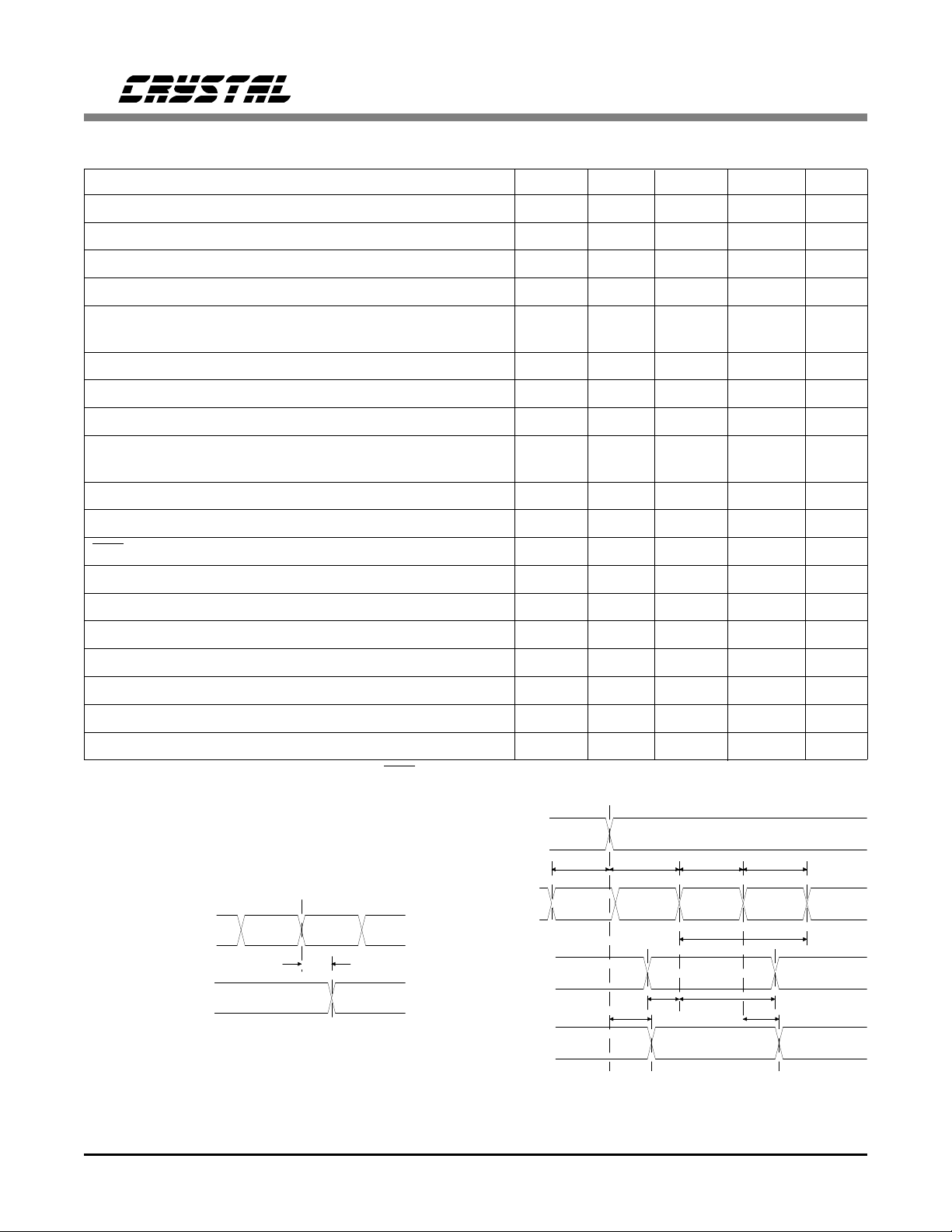
ANALOG CHARACTERISTICS( T
Word Clock = 48 kHz (PLL in use); Measurement Bandwidth is 20 Hz to 20 kHz; Local components as shown
in "Recommended Connection Diagram"; SPI mode, Format 0, unless otherwise specified.)
Parameter * Symbol Min Typ Max Units
Analog Input Characteristics
ADC Resolution Audio channels 16 - - Bits
ADC Differential Nonlinearity - - ±0.9 LSB
Dynamic Range Audio channels(A weighted): 82 85 - dB
Total Harmonic Distortion + Noise (A weighted) THD+N - -85 -82 dB
Interchannel Isolation - 85 - dB
Interchannel Gain Mismatch - - .1 dB
Frequency Response Audio channels(0 to 0.454 Fs): -3.0 - +0.2 dB
Programmable Input Gain -0.2 - 46.7 dB
Gain Step 1.3 1.5 1.7 dB
Offset Error - 10 - LSB
Full Scale Input Voltage (Auxiliary and Audio channels): 2.66 2.8 2.94 V
Gain Drift - 100 - ppm/°C
- Minimum gain setting (0 dB); unless otherwise specified.
= 25°C; VA+, VD+ = +5V; Full Scale Input Sine wave, 1 kHz;
A
Auxiliary channel 12 Bits
pp
Input Resistance (Note 1) 10 - - kΩ
Input Capacitance - - 15 pF
CMOUT Output Voltage 1.9 2.1 2.3 V
Notes: 1. Input resistance is for the input selected. Non-s elected inputs have a very high (>1MΩ) input
resistance. The input resistance will vary with gain value selected, but will always be greater
than the min. value specified.
Parameter definitions are given at the end of this data sheet.
*
Specifications are subject to change without notice.
2 DS86PP8
ANALOG CHARACTERISTICS (Continued)
Parameter * Symbol Min Typ Max Units
CS4225
Analog Output Characteristics
DAC Resolution 16 - - Bits
DAC Differential Nonlinearity - - ±0.9 LSB
Total Dynamic Range (DAC muted,A weighted) 100 - - dB
Total Harmonic Distortion (Note 2) THD - - 0.01 %
Instantaneous Dynamic Range 85 88 - dB
(DAC not muted, Note 2, A weighted)
Interchannel Isolation (Note 2) - 85 - dB
Interchannel Gain Mismatch - - 0.2 dB
Frequency Response (0 to 0.476 Fs) -3.0 - +0.2 dB
Programmable Attenuation (All Outputs) 0.2 - -117 dB
Attenuation Step 0.88 1.0 1.12 dB
Offset Voltage - 10 - mV
Full Scale Output Voltage (Note 2) 2.66 2.8 2.94 V
Gain Drift - 100 - ppm/°C
Deviation from Linear Phase - - 5 Degrees
Out of Band Energy (Fs/2 to 2Fs) - -60 - dB
- Minimum Attenuation; Unless Otherwise Specified.
pp
Analog Output Load Resistance: 8 - - kΩ
Capacitance: - - 100 pF
Power Supply
Power Supply Current Operating - 120 TBD mA
Power Down - 1 TBD mA
Power Supply Rejection (1 kHz) - 40 - dB
Notes: 2. 10 k Ω, 100 pF load.
DS86PP8 3
CS4225
16-Bit Audio A/D Decimation Filter Characteristics (See graphs towards the
end of this data sheet)
Parameter Symbol Min Typ Max Units
Passband ( to -3 dB cor ner) (Fs is conversion freq.) 0 - 0.454Fs Hz
Passband Ripple - - ±0.1 dB
Transition Band 0.40Fs - 0.60Fs Hz
Stop Band ≥ 0.60Fs - - Hz
Stop Band Rejection 75 - - dB
Group Delay - 10/Fs - s
Group Delay Variation vs. Frequency - - 0.0 µs
D/A Interpolation Filter Characteristics (See graphs toward the end of this data sheet)
Parameter Symbol Min Typ Max Units
Passband (to -3 dB corner) (Fs is conversion freq.) 0 - 0.476Fs Hz
Passband Ripple - - ±0.1 dB
Transition Band 0.442Fs - 0.567Fs Hz
Stop Band ≥0.567Fs - - Hz
Stop Band Rejection 50 - - dB
Stop Band Rejection 57 - - dB
with Ext. 2Fs RC filter
Group Delay - 12/Fs - s
Group Delay Variation vs. Frequency - - TBD µs
4 DS86PP8
CS4225
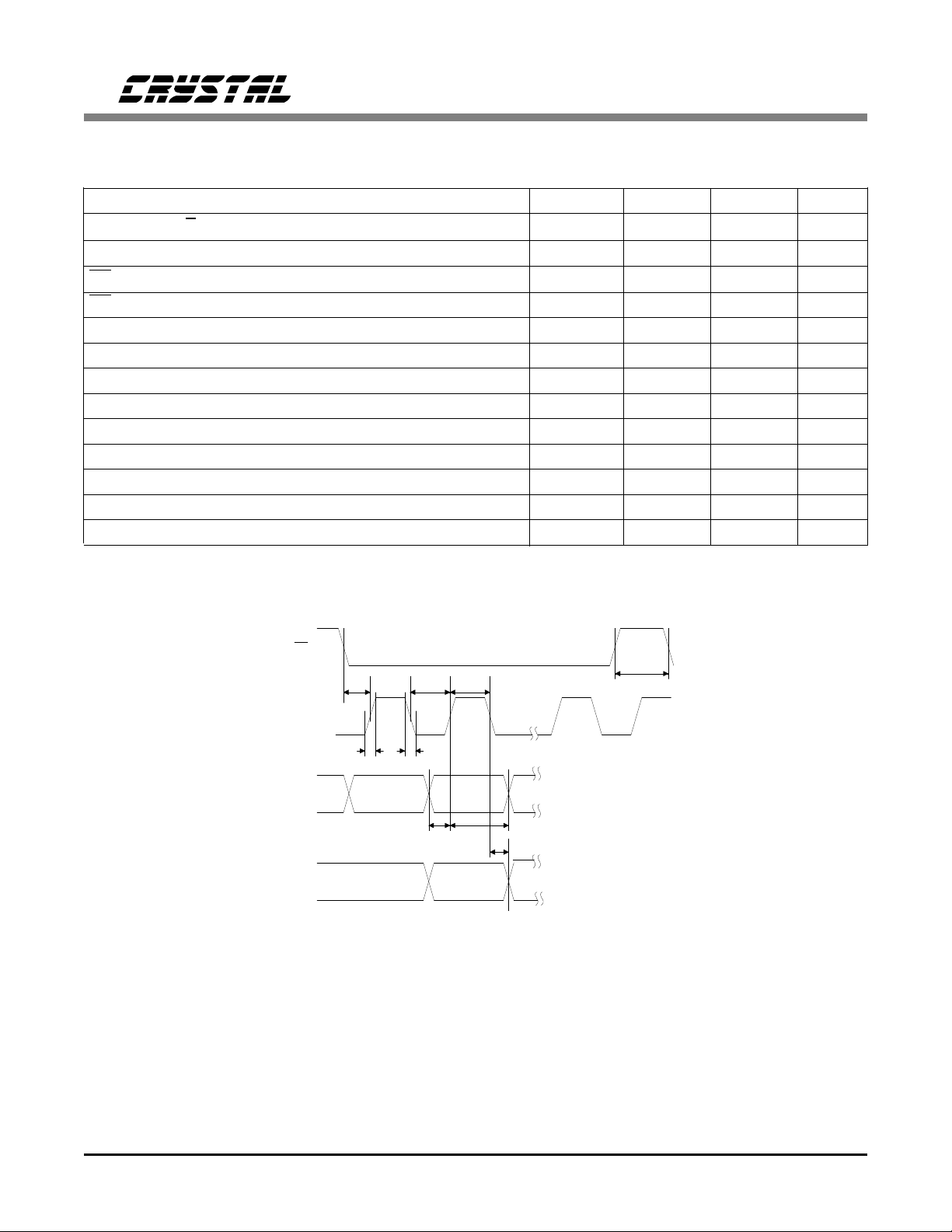
SWITCHING CHARACTERISTICS (T
= 25°C; VA+, VD+ = +5V, outputs loaded with 30pF)
A
Parameter Symbol Min Typ Max Units
SCLK period t
SCLK high time t
SCLK low time t
sckw
sckh
sckl
80 - - ns
25 - - ns
25 - - ns
Input Transition Time 10% to 90% points - - 10 ns
Input Clock Frequency Crystals 32 - 26000 kHz
XTI 32 - 26000 kHz
Input Clock (XTI) low time 30 - - ns
Input Clock (XTI) high time 30 - - ns
Input clock jitter tolerance - 500 - ps
PLL clock recovery frequency LRCK, LRCKAUX 32 - 50 kHz
SCLK, SCLKAUX 2.048 - 3.200 MHz
CLKOUT duty cycle 45 50 55 %
Audio ADC’s & DAC’s sample rate Fs 4 - 50 kHz
RST-PDN low time (Note 5) 500 - - ns
MSB output from LRCK edge (Format 1 and 3) t
SDOUT output from SCLK edge t
SDIN setup time before SCLK edge t
SDIN hold time after SCLK edge t
LRCK to SCLK delay (slave mode) t
LRCK to SCLK setup (slave mode) t
LRCK to SCLK alignment (master mode) t
Note: 5. After Powering up the CS4225,
RST-PDN should be held low for 50 ms to allow the voltage
lrpd
dpd
ds
dh
lrckd
lrcks
mslr
- - 50 ns
- - 50 ns
- - 35 ns
- - 35 ns
35 - - ns
35 - - ns
-20 - 20 ns
reference to settle.
LRCK
LRCKAUX
SCLK*
SCLKAUX*
(output)
t
mslr
LRCK
LRCKAUX
(output)
Audio Ports Master Mode Timing
(input)
SCLK*
SCLKAUX*
(input)
SDIN1
SDIN2
DATAUX
SDOUT1
SDOUT2
*Active edge of SCLK, SCLKAUX depends on selected format.
t
lrckd
t
lrpd
t
lrcks
t
t
sckh
t
t
ds
dh
MSB MSB-1
t
sckw
sckl
t
dpd
Audio Ports Slave Mode and Data I/O timing
DS86PP8 5
SWITCHING CHARACTERISTICS - CONTROL PORT
(TA = 25oC VD+, VA+ = 5V±10%; Inputs: logic 0 = DGND, logic 1 = V D+, CL = 30pF)
Parameter Symbol Min Max Units
(H/
SPI Mode
CCLK Clock Frequency f
CS High Time Between Transmissions t
CS Falling to SCK Edge t
CCLK Low Time t
CCLK High Time t
CDIN to CCLK Rising Setup Time t
CCLK Rising to DATA Hold Time CDIN (Note 9) t
CCLK Falling to CDOUT stable t
Rise Time of CDOUT t
Fall Time of CDOUT t
Rise Time of CCLK and CDIN t
Fall Time of CCLK and CDIN t
Notes: 9. Data mus t be held for sufficient time to bridge the transition time of CCLK.
S=0)
sck
csh
css
scl
sch
dsu
dh
01MHz
1.0 µs
20 ns
500 ns
500 ns
250 ns
50 ns
pd
r1
f1
r2 100 ns
f2
CS4225
250 ns
25 ns
25 ns
100 ns
CS
CCLK
CDIN
CDOUT
t
css
t
r2
t
t
sch
scl
t
t
f2
dsu
t
t
dh
pd
t
csh
6 DS86PP8
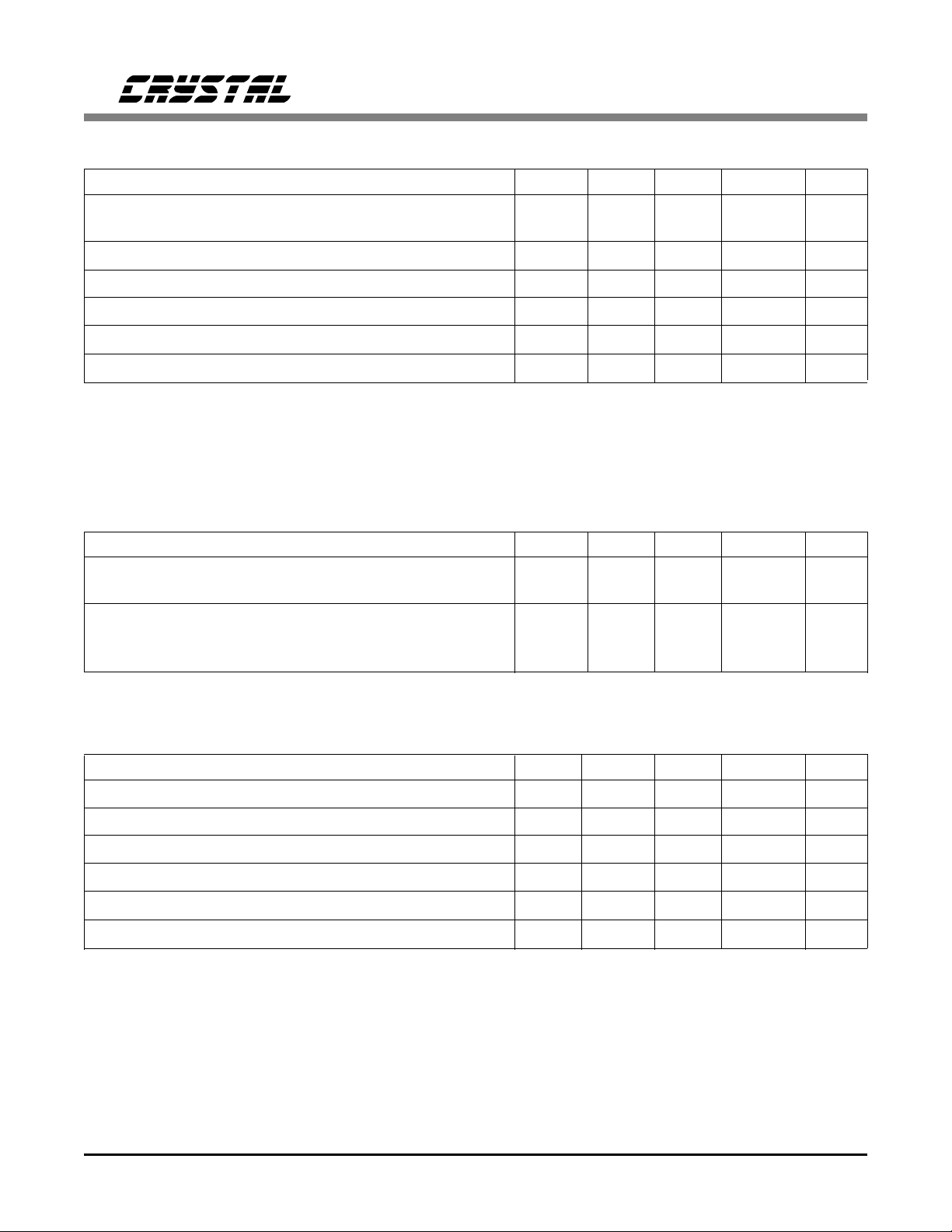
SWITCHING CHARACTERISTICS - CONTROL PORT
(TA = 25oC; VD+, VA+ = 5V±10%;Inputs: logic 0 = DG ND, logic 1 = VD+, CL = 20pF)
Parameter Symbol Min Max Units
(H/
I2C® Mode
S = floating) Note 10
CS4225
SCL Clock Frequency f
Bus Free Time Between Transmissions t
Start Condition Hold Time (prior to first clock pulse) t
Clock Low Time t
Clock High Time t
Setup Time for Repeated Start Condition t
SDA Hold Time from SCL Falling Note 11 t
SDA Setup Time to SCL Rising t
Rise Time of Both SDA and SCL Lines t
Fall Time of Both SDA and SCL Lines t
Setup Time for Stop Condition t
2C®
Notes: 10. Use of the I
2C®
is a registered trademark of Philips Semiconductors.
I
bus interface requires a license from Philips.
11. Data mus t be held for sufficient time to bridge the 300ns transition time of SCL.
scl
buf
hdst
low
high
sust
hdd
sud
r
f
susp
0 100 kHz
4.7 µs
4.0 µs
4.7 µs
4.0 µs
4.7 µs
0 µs
250 ns
1 µs
300 ns
4.7 µs
Repeated
Start
t
sust
t
hdst
Stop
t
f
t
r
t
susp
SDA
SCL
Stop Start
t
buf
t
hdst
t
low
t
hdd
t
high
t
sud
DS86PP8 7
CS4225
ABSOLUTE MAXIMUM RATINGS (AGND, DGND = 0V, all voltages with respect to 0V.)
Parameter Symbol Min Typ Max Units
Power Supplies: Digital VD -0.3 - 6.0 V
Analog VA -0.3 - 6.0 V
Input Current (Except Supply Pins) - - ±10.0 mA
Analog Input Voltage -0.3 - (VA+)+0.3 V
Digital Input Voltage -0.3 - (VD+)+0.3 V
Ambient Temperature (Power Applied) -55 - +125 °C
Storage Temperature -65 - +150 °C
Warning: Operation at or beyond these limits may result in permanent damage to the device.
Normal operation is not guaranteed at these extremes.
RECOMMENDED OPERATING CONDITIONS (AGND, DGND = 0V, all voltages with
respect to 0V.)
Parameter Symbol Min Typ Max Units
Power Supplies: Digital VD 4.6 5.0 5.4 V
Analog VA 4.6 5.0 5.4 V
Operating Ambient Temperature CS4225-KL 0 25 70 °C
CS4225-BL T
CS4225-YU -40 25 +85 °C
DIGITAL CHARACTERISTICS (T
Parameter Symbol Min Typ Max Units
High-level Input Voltage V
Low-level Input Voltage V
High-level Output Voltage at I0 = -2.0 mA V
Low-level Output Voltage at I0 = 2.0 mA V
Input Leakage Current (Digital Inputs) - - 10 µA
Output Leakage Current (High-Z Digital Outputs) - - 10 µA
= 25°C; VA+, VD+ = 5V)
A
A
IH
IL
OH
OL
-40 25 +85 °C
(VD+)-1.0 - (VD+)+0.3 V
-0.3 - 1.0 V
(VD+)-0.3 - - V
--0.1V
8 DS86PP8
CS4225
+5V
Supply
To Optional
Inp u t Bu ffe rs
0.01 µF
NPO
0.47 µF
Fe rrite B e a d
150
0.01
µ
NPO
Digital
Audio
Source
Mode
Setting
and
Hardware
Controls
1 µF
+
0.47 µF
1.0 µF
1.0 µF
1.0 µF
1.0 µF
1.0 µF
1.0 µF
0.01 µF
NPO
F
38
33
39
37
13
12
2.0
0.1 µF
1 µF
+
3
23
CMOUT
19
AIN1L
18
AIN1R
16
AIN2L
17
AIN2R
15
AIN3L
CS4225
14
AIN3R
21
CR
22
20
4
5
6
CL
AINAUX
DATAUX
LRCKAUX
SCLKAU X
SCL/CCLK/IF0
SDA/CDOUT/CKF0
AD3/CS/IF1
AD2/CDIN/CKF1
DIF/HOLD
RST-PDN
H/S
DEM
IS0/ADO
IS1/AD1
AGND1,2
DGND
FILT
25 31 2 32 35 34
0.2 µF
F
0.1
µ
26
VAVD
AOUT1
AOUT2
AOUT3
AOUT4
VREF
SDIN1
SDIN2
SDOUT1
SDOUT2
LRCK
SCLK
CLKOUT
OVL
XTO XTI
C2C1
+5V Analog (optional)
If a separate +5V an alog supply
is available, attach here and
remove the 2.0 resistor
600
27
µ
0.0022
28
0.0022
29
0.0022
NPO
600
NPO
600
F
F
µ
F
µ
NPO
600
30
µ
0.0022
24
F
NPO
0.1 µF
7
9
10
8
43
42
1
44
41
40
36
11
External
Clock
Input
+
> 1.8 µF
>
+
> 1.8 µF>
+
>
> 1.8
+
> 1.8 µF
>
+
MicroController
Audio
DSP
10
47 k
47k
47 k
F
µ
47 k
F
µ
All unused inputs
should be tied to 0V.
All NC pins should
b e left flo ating .
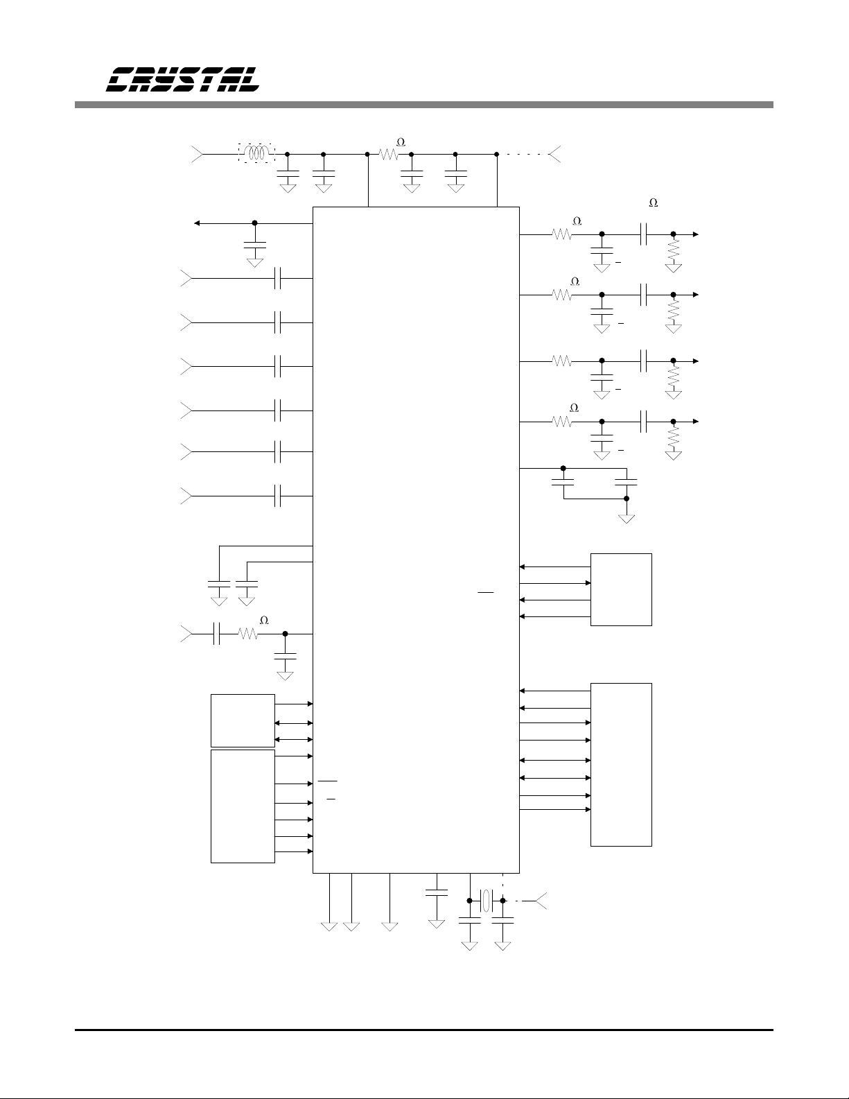
Figure 1 - Recommended Connection Diagram
DS86PP8 9

CS4225
FUNCTIONAL DESCRIPTION
Overview
The CS4225 has 2 channels of 16-bit analog-todigital conversion and 4 channels of 16-bit
digital-to-analog conversion. An auxiliary 12-bit
ADC is also provided. The ADCs and the DACs
are delta-sigma type converters. The ADC inputs
have adjustable input gain, while the DAC outputs have adjustable output attenuation.
Digital audio data for the DACs and from the
ADCs is communicated over a serial port. Separate pins for input and output data are provided,
allowing concurrent writing to and reading from
the device. Control for the functions available on
the CS4225 are communicated over a serial microcontroller style interface, or may be set via
dedicated mode pins. Figure 1 shows the recommended connection diagram for the CS4225.
Analog Inputs
Line Level Inputs
AIN1R, AIN1L, AIN2R, AIN2L, AIN3R, AIN3L
and AINAUX are the line level input pins (See
Figure 1). These pins are internally biased to the
CMOUT voltage (nominally 2.1V). A 1µF DC
blocking capacitor allows signals centered
around 0V to be input. Figure 2 shows an optional dual op amp buffer which combines level
shifting with a gain of 0.5 to attenuate the standard line level of 2V
rms
to 1V
. The CMOUT
rms
reference level is used to bias the op amps to
approximately one half the supply voltage.
Series DC blocking capacitors eliminate the contribution of signal offset to the A/D converters.
The CS4225 offset calibration scheme yields
minimum DC offset values assuming that the inputs are AC coupled (DC blocking capacitor
present). If a DC blocking capacitor is not used,
a greater DC offset will occur. This offset could
be as high as + 70 codes, with no gain.
56 pF
Line In
Right
Example
Op-Amps
MC34074
Line In
Left
1.0 uF
are
1.0 uF
Op-amps are run
from VA+ (+5V)
and AGND.
Figure 2 - Optional Line Input Buffer
20 k
0.47 uF
20 k
_
+
+
_
10 k
5 k
10 k
1.0 uF
AINxR
CMOUT
0.47 uF
1.0 uF
AINxL
56 pF
The input pair for the 16-bit ADCs is selected by
IS0 and IS1, which are accessible in the Input
Selection Byte in software mode or dedicated
pins in the hardware mode. Antialiasing filters
follow the input mux, providing antialiasing for
the input channels. These filters consist of internal resistors and external capacitors attached to
the CR and CL pins. The CR and CL capacitors
must be low voltage coefficient type, such as
NPO.
The analog signal is input to the 12-bit ADC via
the AINAUX pin. An antialiasing filter of 150Ω
with 0.01µF to ground is required (See Figure 1)
along with a series DC blocking capacitor. The
AINAUX signal is normally routed to the 12-bit
ADC. This signal may also be routed to the Left
16-bit ADC (replacing the selected left input),
under control of the AIM bit in the 12-bit ADC
Mode Byte. In this mode, the input antialiasing
filters and gain adjustment operates on the
AINAUX signal.
Adjustable Input Gain
The signals from the line inputs are routed to a
programmable gain circuit which provides up to
10 DS86PP8

CS4225
46.5dB of gain in 1.5dB steps. The gain is adjustable only by software control. Level changes
only take effect on zero crossings to minimize
audible artifacts. If there is no zero crossing,
then the requested level change will occur after a
time-out of 511 frames (10.6ms at 48kHz frame
rate). There is a separate zero crossing detector
for each channel.
Analog Outputs
Line Level Outputs
AOUT1, AOUT2, AOUT3 and AOUT4 output a
1V
level for full scale, centered around
rms
+2.1V. Figure 1 shows the recommended 1.0µF
dc blocking capacitor with a 40kΩ resistor to
ground. When driving impedances greater than
10kΩ, this provides a high pass corner of 20Hz.
These outputs may be muted.
Output Level Attenuator
The DAC outputs are each routed through an attenuator, which is adjustable in 1dB steps.
Output attenuation is available via software control only. Level changes are implemented such
that the noise is attenuated by the same amount
as the signal (equivalent to using an analog attenuator after the signal source), until the
residual output noise is equal to the noise floor
in the mute state. Level changes only take effect
on zero crossings to minimize audible artifacts.
If there is no zero crossing, then the requested
level change will occur after a time-out of 511
frames (10.6ms at 48kHz frame rate). There is a
separate zero crossing detector for each channel.
Each output can be independently muted via
mute control bits. In addition, the CS4225 has an
optional mute on consecutive zeros feature,
where each DAC output will mute if it receives
512 consecutive zeros. A single non-zero value
will unmute the DAC output.
ADC and DAC Coding
The CS4225 converters use 2’s complement coding. Table 1 shows the ADC and DAC transfer
functions.
16-bit ADC/DAC 12-bit ADC
Input/ 2’s 2’s Input
Output Complement Complement Voltage*
Voltage* Code Code
+1.400000 7FFF 7FF +1.40000
+1.399957 7FFE 7FE +139864
+0.000064 0001 001 +0.00204
+0.000021 0000 000 +0.00068
-0.000021 FFFF FFF -0.00068
-0.000064 FFFE FFE -0.00204
-1.399957 8001 801 -1.39864
-1.400000 8000 800 -1.40000
*Nominal voltage relative to CMOUT (Typ 2.1V), no
gain or attenuation. Actual measured voltage will be
modified by the gain error and offset error specifications.
Table 1 - ADC/DAC Input and Output Coding Table
Calibration
Both output offset voltage and input offset error
are minimized by an internal calibration cycle.
At least one calibration cycle must be invoked
after power up. A calibration will occur any time
the part comes out of reset, including the powerup reset. For the most accurate calibration, some
time must be allowed between powering up the
CS4225, or exiting the power-down state, and initiating a calibration cycle, to allow the voltage
reference to settle. This is achieved by holding
RST/PDN low for at least 50ms after power up
or exiting power-down mode. Input offset error
will be calibrated for all inputs and outputs.
A calibration takes 192 frames to complete,
based on the frequency of the VCO of the inter-
DS86PP8 11

CS4225
nal PLL. The calibration that occurs following a
reset will proceed at a rate determined by the
free running VCO in software mode (which will
be at a Fs of about 40kHz), or the selected clock
input in hardware mode.
The CS4225 can be calibrated whenever desired.
A control bit, CAL, in the Control Byte, is provided to initiate a calibration. The sequence is:
1) Set CAL to 1, the CS4225 sets CALD to 1
and begins to calibrate.
2) Wait for CALD to go to 0. CALD will go to 0
when the calibration is done.
3) Set CAL to 0 for normal operation.
Clock Generation
The master clock to operate the CS4225 may be
generated by using the on-chip crystal oscillator,
by using the on-chip PLL, or by using an external clock source. If the active clock source stops
for 5µs, the CS4225 will enter a power down
state to prevent overheating. In all modes it is
desirable to have SCLK & LRCK synchronous
to the selected master clock.
Clock Source
The CS4225 requires a high frequency (256 Fs)
clock to run the internal logic. The Clock Source
bits, CS0/1/2, in the Clock Mode Byte determine
the source of the clock. A high frequency crystal
can be attached to XTI and XTO, or a high frequency clock can be input into XTI. In both
these cases, the internal PLL is disabled, with
the VCO shut off. The externally supplied high
frequency clock can be 256 Fs, 384 Fs or
512 Fs. The CI0/1 bits in the Clock Mode Byte
must be set accordingly. When using the on-chip
crystal oscillator, external loading capacitors are
required (see Figure 1). High frequency crystals
(> 8 MHz) should be parallel resonant, fundamental mode and designed for 20pF loading
(equivalent to 40pF to ground on each leg). An
example crystal supplier is CAL crystal
(714) 991-1580.
Alternatively, the on-chip PLL may be used to
generate the required high frequency clock. The
PLL input clock is either 1 Fs, 32 Fs or 64 Fs
and may be input from the Auxiliary Port, (either
LRCKAUX or SCLKAUX), the DSP port,
(either LRCK or SCLK), or from XTI/XTO. In
this last case, a 1 Fs clock may be input into
XTI, or a 1 Fs crystal attached across XTI/XTO.
The gain of the internal inverter is adjusted for
the low crystal frequency. Using a clock at 64 Fs
will result in less PLL clock jitter than a clock at
1 Fs. The PLL will lock onto a new 1 Fs clock
within 5,000 Fs periods. If the PLL input clock
is removed, the VCO will drift to the low frequency end of its frequency range.
In software mode, bits CS2/1/0 in the Clock
Mode Byte establish the clock source and frequency. In Hardware mode, either LRCKAUX is
the clock reference, at 1 Fs, or the clock may be
input to XTI.
Master Clock Output
CLKOUT is a master clock output provided to
allow synchronization of external components.
Available CLKOUT frequencies of 1 Fs, 256 Fs,
384 Fs, and 512 Fs, are selectable by the CO0/1
bits of the Clock Mode Byte. When switching
between clock sources, CLKOUT will always remain low or high for > 10ns.
Synchronization
In normal operation, the DSP port and Auxiliary
port operate synchronously to the CS4225 clock
source. It is advisable to mute the DACs when
changing from one synchronization source to another to avoid the output of undesirable audio
signals as the CS4225 resynchronizes. If data
which is not synchronous to the clock source is
input to the CS4225, then samples will be
dropped or repeated, which will cause audible
artifacts. Under such conditions, the CS4225
may not meet all data sheet performance specifications.
12 DS86PP8

CS4225
FORMAT 0:
FORMAT 1:
FORMAT 2:
FORMAT 3:
LRCK
SCLK
SDIN
LRCK
SCLK
SDIN
LRCK
SCLK
SDIN
LRCK
SCLK
Left
MSB
MSB LSB MSB LSB MSB
LSB
LSB
Left
Left
MSB LSB MSB
Left
MSB LSB
Right
Right
Right
Right
MSB
LSB
FORMAT 0
FORMAT 1
FORMAT 2
FORMAT 3
SDIN
MSB LSB MSB LSB MSB
Figure 3 - Audio DSP and Auxiliary Port Data Input Formats.
LRCK
SCLK
SDOUT
LRCK
SCLK
SDOUT
LRCK
SCLK
SDOUT
LRCK
SCLK
SDOUT
LSB
Left
MSB LSB
MSB
MSB
MSB
Left
Left
Left
LSB
LSB
MSB
MSB
LSB
MSB
Right
Right
Right
MSB
Right
LSB
LSB
LSB
MSB
MSB
LSB
MSB
Figure 4 - Audio DSP Port Data Output Formats.
DS86PP8 13

LRCK
SCLK
CS4225
LSB
MSB
DAC #2
MSB
Right ADC
SDIN1
SDOUT1
MSB LSB
DAC #1
MSB
Left ADC
Figure 5 - One data line mode (Forma t 4)
Digital Interfaces
There are 3 digital interface ports: the audio DSP
port, the auxiliary digital audio port and the control port. In hardware mode (H/S pin high) the
control port is disabled, and various modes can
be set via pins. In hardware mode, control of the
input gain, output level and some modes are not
possible.
Audio DSP Serial Interface Signals
The serial interface clock, SCLK, is used for
transmitting and receiving audio data. SCLK can
be generated by the CS4225 (master mode) or it
can be input from an external SCLK source
(slave mode). The number of SCLK cycles in
one system sample period is programmable to be
32, 48, or 64. When SCLK is an input, 32
SCLK’s per system sample period is not recommended, due to potential interference effects; 64
SCLK’s per sample period should be used instead.
LSB
LSB
MSB
DAC #3
MSB
AUX ADC
12-Bits
LSB MSB
MSB
0
12-Bits
DAC #4
4 0's4 0's AUX ADC
LSB
0
MSB
MSB
data is for DAC #4. SDOUT1 carries the data
from the 2 16-bit ADCs. SDOUT2 carries the
data from the 12-bit ADC. The audio DSP port
may also be configured so that all 4 DAC’s data
is input on SDIN1, and all 3 ADC’s data is output on SDOUT1.
Audio DSP Serial Interface Formats
The audio DSP port supports 5 alternate formats,
shown in Figures 3, 4, and 5. These formats are
chosen through the DSP Port Mode Byte in software mode. In hardware mode, four formats are
available as selected by the DIF and IF0 pins.
The 12-bit ADC data format is similar to the 16bit data format. The 12-bit data is positioned to
the most significant end of a 16-bit field, with
the lower 4 bits set to zero. The resulting 16-bit
value is output on SDOUT2 in both the left and
right channel positions. The format will be the
same as the selected SDOUT1 format.
Figure 5 shows the timing for format 4, where
The Left/Right clock (LRCK) is used to indicate
left and right data, also the start of a new sample
period. It may be output from the CS4225, or it
all 4 DAC data words are presented on SDIN1,
and the 3 ADC data words are presented on
SDOUT1.
may be generated from an external controller.
The frequency of LRCK is equal to the system
sample rate, Fs.
Format 5 is a combination mode. The data output is as in Format 1, on the SDOUT1 and
SDOUT2 pins. The data input is as in Format 4
SDIN1 and SDIN2 are the data input pins, each
of which drives a pair of DACs. SDIN1 left data
on SDIN1. In both format 4 and 5, LRCK duty
cycle is 50% if it is an output.
is for DAC #1, SDIN1 right data is for DAC #2,
SDIN2 left data is for DAC #3, and SDIN2 right
14 DS86PP8

CS
CCLK
CDIN
CHIP
ADDRESS
AD0
AD1
0
R/W
MAP
MSB
byte 1
DATA
LSB
byte n
CHIP
ADDRESS
AD0
AD1
0
CS4225
R/W
CDOUT
MAP = Memory Address Pointer
Figure 6 - Control Port Timing, SPI mode
Auxiliary Audio Port Signals
The auxiliary port provides an alternate way to
input digital audio signals into the CS4225, and
allows the CS4225 to synchronize the system to
an external digital audio source. This port consists of clock, data and left/right clock pins
named, SCLKAUX, DATAAUX and
LRCKAUX. These signals are fed through to the
SCLK, SDOUT1 and LRCK pins. There is a two
frame delay from DATAAUX to SDOUT1.
When the auxiliary port is used, the frequency of
LRCKAUX must equal to the system sample
rate, Fs, but no particular phase relationship is
required.
Auxiliary Audio Port Formats
Input data on DATAAUX is clocked into the part
by SCLKAUX using the format selected in the
Auxiliary Port Mode Byte. In hardware mode,
the auxiliary port format is the same as the DSP
port format and is determined by the DIF pin.
The auxiliary audio port supports the same 4 formats as the audio DSP port in 2 data line mode.
LRCKAUX is used to indicate left and right data
samples, and the start of a new sample period.
SCLKAUX and LRCKAUX may be output from
the CS4225, or they may be generated from an
external source, as set by the AMS control bit in
Software mode or IF1 in Hardware mode.
High Z
MSB
LSB
MSB
LSB
Control Port Signals
The control port has 2 modes: SPI and I2C®,
with the CS4225 as a slave device. The SPI
mode is selected by setting the H/S pin low.
I2C mode is selected by floating the H/S pin.
If the H/S pin is floated, add a 0.1µF capacitor
to ground on the H/S pin to minimize noise
pickup.
SPI Mode
In SPI mode, CS is the CS4225 chip select signal, CCLK is the control port bit clock, (input
into the CS4225 from the microcontroller),
CDIN is the input data line from the microcontroller, CDOUT is the output data line to the
microcontroller, and AD0 and AD1 form the
chip address.
The pins AD0, AD1 must be tied to one of 4
possible chip addresses. To write to a particular
CS4225, the AD0, AD1 bits must match the state
of the AD0, AD1 pins for that chip. This allows
up to 4 CS4225 devices to co-exist on one control port bus.
Figure 6 shows the operation of the control port
in SPI mode. To write to a register, bring CS
low. The first 5 bits on CDIN must be zero. The
next 2 bits form the chip address. The eighth bit
is a read/write indicator (R/W), which should be
DS86PP8 15

SDA
SCL
Note 1 Note 2
001
ADDR
AD3-0
R/W
ACK
DATA
1-8
ACK
DATA
1-8
CS4225
ACK
Start
Note 1: The first 3 address bits for the CS4225 must be 001.
Note 2: If operation is a write, this byte contains the Memory Address Pointer, MAP.
Figure 7 - Control Port Timing, I2C® Mode
low to write. The next 8 bits form the Memory
Address Pointer (MAP), which is set to the address of the register that is to be updated. The
next 8 bits are the data which will be placed into
register designated by the MAP. During writes,
the CDOUT output stays in the Hi-Z state. It
may be externally pulled high or low with a
47kΩ resistor.
The CS4225 has a MAP auto increment capability, enabled by the INCR bit in the MAP register.
If INCR is a zero, then the MAP will stay constant for successive reads or writes. If INCR is
set to a 1, then MAP will auto increment after
each byte is read or written, allowing block reads
or writes of successive registers.
To read a register, the MAP has to be set to the
correct address by executing a partial write cycle
which finishes (CS high) immediately after the
MAP byte. The auto MAP increment bit (INCR)
may be set or not, as desired. To begin a read,
bring CS low, send out the chip address and set
the read/write bit (R/W) high. The next falling
edge of CCLK will clock out the MSB of the
addressed register (CDOUT will leave the high
impedance state). If the MAP auto increment bit
is set to 1, the data for successive registers will
appear consecutively.
Stop
clock, SCL, with the clock to data relationship as
shown in Figure 7. There is no CS pin. Pins
AD0, AD1, AD2, AD3 form the chip address.
The upper 3 bits of the 7 bit address field must
be 001. To communicate with a CS4225, the
LSBs of the chip address field, which is the first
byte sent to the CS4225, should match the settings of the AD0, AD1, AD2, AD3 pins. The
eighth bit of the address bit is the R/W bit (high
for a read, low for a write). If the operation is a
write, the next byte is the Memory Address
Pointer which selects the register to be read or
written. If the operation is a read, the contents of
the register pointed to by the Memory Address
Pointer will be output. Setting the auto increment bit in MAP, allows successive reads or
writes of consecutive registers. Each byte is
separated by an acknowledge bit. Use of the I2C
bus®compatible interface requires a license from
Philips. I2C bus® is a registered trademark of
Philips Semiconductors.
Control Po rt Bit Defi nitions
All registers can be written and read back, except the status report byte, which is read only.
See the following bit definition tables for bit assignment information.
I2C ®Mode
In I2C® mode, SDA is a bidirectional data line.
Data is clocked into and out of the part by the
16 DS86PP8

CS4225
Memory Address Pointer (MAP)
B7 B6 B5 B4 B3 B2 B1 B0
INCR 0 0 0 MAP3 MAP2 MAP1 MAP0
MAP3-MAP0 Register Function
0 - Reserved
1 - Output Attenuator 1
2 - Output Attenuator 2
3 - Output Attenuator 3
4 - Output Attenuator 4
5 - Input Gain 1
6 - Input Gain 2
7 - Auxiliary Port Mode
8 - DSP Port Mode
9 - Clock Mode
10 - Control Byte
11 - Status Repor t Byte
12 - Input Channel Select
13 - Aux Control Byte
14 - Reser ved
15 - Reser ved
INCR Auto Increment Control Bit
0 - No auto increment
1 - Auto increment on
Auxiliary Port Mode Byte (7)
B7 B6 B5 B4 B3 B2 B1 B0
0 0 0 AMS ACK1 ACK0 ADF1 ADF0
ADF1 - ADF0 Sets Digital Interface Format
0 - Format 0 - I
1 - Format 1
2 - Format 2
3 - Format 3
ACK1 - ACK0 Sets number of bit clocks per Fs period
0 - 64
1 - 48 - gated 64Fs
2 - 32 - gated 64Fs
3 - 32 - continuous
AMS AUX Master /Slave control bit
0 - port is master (SCLKAUX and
LRCKAUX are outputs).
1 - port is slave (SCLKAUX and
LRCKAUX are inputs).
2
S
DSP Port Mode Byte (8)
B7 B6 B5 B4 B3 B2 B1 B0
0 0 DMS DCK1 DCK0 DDF2 DDF1 DDF0
Output Attenuator Data Byte (1, 2, 3, 4)
B7 B6 B5 B4 B3 B2 B1 B0
0 ATT6 ATT5 ATT4 ATT3 ATT2 ATT1 ATT0
ATT6 to Sets Attenuator Level
ATT0 0 - No attenuation
127 - 127 dB attenuation
ATT0 represents 1.00 dB
Input Gain Setting Data Byte (5, 6)
B7 B6 B5 B4 B3 B2 B1 B0
0 0 0 GN4 G N3 GN2 GN1 GN0
GN4 to Sets Input Gain
GN0 0 - No gain
31 - 46.5 dB gain
GN0 represents 1.5 dB
DDF2 - DDF0 Sets Digital Interface Format
0 - Format 0 - I
1 - Format 1
2 - Format 2
3 - Format 3
4 - One data pin in, One data pin out
mode (Format 4).
5 - Output is Format 1 on SDOUT1
and SDOUT2, input is Format 4
on SDIN1.
DCK1 - DCK0 Set number of bit clocks per Fs period
0 - 64
1 - 48 - gated 64 Fs
2 - 32 - gated 64 Fs
3 - 32 - continuous
DMS DSP Master /Slave control bit
0 - port is master (SLCK and LRCK
are outputs).
1 - port is slave (SLCK and LRCK
are inputs).
2
S
DS86PP8 17

CS4225
Clock Mode Byte (9)
B7 B6 B5 B4 B3 B2 B1 B0
0 CO1 CO0 CI1 CI0 CS2 CS1 CS0
CS1 - CS0 Sets the source of the master clock
which runs the CS4225.
0 - Crystal Os cillator or XTI (PLL D isabled)
1 - PLL driven by LRCKAUX at 1 Fs
2 - PLL driven by LRCK at 1 Fs
3 - PLL driven by XTI/XTO (XTI at 1 Fs)
4 - PLL driven by SCLK at 32 Fs
5 - PLL driven by SCLK at 64 Fs
6 - PLL driven by SCLKAUX at 32 Fs
7 - PLL driven by SCLKAUX at 64 Fs
Cl1 - CI0 Determines frequency of XTI
when PLL is disabled.
0 - 256 Fs
1 - 384 Fs
2 - 512 Fs
3 - Reserved
CO1-CO0 Determines CLKOUT frequency
0 - 256 Fs
1 - 384 Fs
2 - 512 Fs
3 - 1 Fs
Control Byte (10)
B7 B6 B5 B4 B3 B2 B1 B0
MUTC CAL DEMC DEM MUT4 MUT3 MUT2 MUT1
MUT4 to Mute Control Bits
MUT1 0 - Nor mal Output Level
1 - Selected DAC output muted
DEM Selects De-Emphasis
0 - Normal Flat DAC frequency response
1 - CD De-Emphasis Selected
DEMC Selects De-Emphasis Contr ol Source
0 - De-emphasis is controlled by DEM
pin. DEM bit is ignored.
1 - De-emphasis is controlled by DEM bit.
DEM pin is ignored.
CAL 0 - Normal Operation
1 - Initiate Calibration
MUTC Controls mute on consecutive zeros
function
0 - 512 consecutive zeros will mute DAC
1 - DAC output will not mute on zeros.
Status Report Byte (11)
B7 B6 B5 B4 B3 B2 B1 B0
OVL1 OVL0 OV12 ACK 0 LOCK CALD 0
OVL1 to 16 - bit ADC overload bits.
OVL0 00 - Nor mal ADC input levels
01 - -6 dB level
10 - -3 dB level
11 - Clipping
Indicates one of the ADC’s has been
overdriven. These bits are "sticky".
They will stay set until read, when they
will return to 00 if the overload is no
longer present.
OV12 12-bit ADC overload bit
0 - normal input
1 - clipped input
This bit is also "sticky"
ACK C ontrol port data check bit
0 - Multiple of 8 clocks received
last word (SPI Mode)
1 - Error, not multiple of 8 clocks received.
LOCK PLL lock indicator
0 - PLL not locked. If PLL is selected,
DAC outputs will mute
1 - PLL locked
CALD 0 - Calibration done
1 - Calibration in progress
Input Selection Byte (12)
B7 B6 B5 B4 B3 B2 B1 B0
000000IS1IS0
IS1 - IS0 Select input channel
0 - Select AIN1
1 - Select AIN2
2 - Select AIN3
3 - Select Auxiliary Digital Input Port
Aux Control Byte (13)
B7 B6 B5 B4 B3 B2 B1 B0
AIM0000000
AIM Auxiliary Input Mode Control Bit
0 - AINAUX signal is routed to 12-bit ADC
1 - AINAUX routed to AINL of 16-bit ADC
18 DS86PP8

CS4225
Reset
RST-PDN going low causes all the internal control registers, used in software mode, to be set to
the states indicated in Table 1. The reset states
are different for hardware mode, see the section
on Hardware Mode. RST-PDN must be brought
low and high at least once after power up. RSTPDN returning high causes the CS4225 to
execute an offset calibration cycle. RST-PDN returning high should occur at least 50ms after the
power supply has stabilized.
Power Down Mode
Placing the RST-PDN pin into a high impedance
state (floating) puts the CS4225 into the power
down mode. This may be done by driving the
RST-PDN pin with a three-state buffer, and setting the buffer to the hi-z state. In power-down
mode CMOUT and VREF will not supply cur-
ATT6 → ATT0 = 127 CS2, CS1,CS0 = 3
GN4 → GN0 = 0 CI1, CI0 = 0
ADF1, ADF0 = 0 CO1, CO0 = 0
ACK1 , ACK 0 = 0 M UT 4 →MUT1 = 1111
AMS = 1 DEM = 0
DDF2 → DDF0 = 0 DEMC = 0
DCK1, DCK1 = 0 MUTC = 0
DMS = 1 IS1, IS0 = 0
MAP = 0 AIM = 0
CAL = 0
Table 1 - Reset State (S oftware Mode )
rent. If the master clock source stops, the
CS4225 will power down after 5µs. Power down
will change all the control registers to the reset
state shown in Table 1.
After returning to normal operation from power
down, an offset calibration cycle must be executed. To leave the power-down state, pull
RST-PDN low for at least 50ms to allow the internal voltage reference time to settle, then high
to initiate an offset calibration cycle.
De-Emphasis
Figure 8 shows the de-emphasis curve. De-emphasis may be enabled under hardware control,
using the DEM pin, or by software control using
the DEM bit. In software mode, either hardware
or software control of de-emphasis may be selected.
The de-emphasis corner frequencies are as
shown in Figure 8 for a sample rate of 44.1kHz.
Selection of de-emphasis at other sample rates
will cause the filter to be applied, but with corner frequencies scaled proportionally to the
sample rate.
Hold Function (Software Mode only)
If the digital audio source has an invalid data
output pin, then the CS4225 may be configured
to cause the last valid analog output level to be
held constant. (This sounds much better than a
potentially random output level.) HOLD is sampled on the active edge of SCLK. If HOLD is
driven high any time during the stereo sample
period, both pairs of DAC’s hold their current
output level, and reject the data currently being
input. SDIN input data is ignored while the
HOLD pin is high. For normal operation, the
HOLD pin must be low.
Gain
dB
(0.072 Fs)
T1=50us*
0dB
(0.241 Fs)
T2 = 15us*
-10dB
F1 F2
* with Fs = 44.1 kHz
Figure 8 - De-emphasis Curve.
Frequency
DS86PP8 19

CS4225
Hardware Mode
Hardware mode is selected by connecting the
H/S pin to VD. In hardware mode, only certain
functions are available:
- de-emphasis,
- digital interface formats 0, 1 and 2, and DSP
format 4,
- auxiliary audio port master/slave selection,
- CLKOUT and XTI frequencies are restricted,
- use of PLL is tied to master/slave selection,
- the PLL locks to L RCKAUX only,
- will mute on consecutive zeros.
In addition, the input gain is set to 0dB (no
gain), and the attenuator is set to 0dB (no attenuation). The DAC mute bits are set to 0 (not
muted). The DSP port and Auxiliary port serial
clocks are set to 64 bits per Fs period.
In hardware mode, the DSP port is always in
slave mode. The IF1 pin selects the Auxiliary
port to be master or slave (low for master, high
for slave). When the Auxiliary port is a master,
XTI is the clock source and the PLL is off.
CKF0 and CKF1 pins define both XTI and
CLKOUT frequencies as follows:
CKF1 CKF0 XTI CLKOUT
0 0 256 Fs 256 Fs
0 1 384 Fs 256 Fs
1 0 512 Fs 256 Fs
1 1 512 Fs 512 Fs
Functions only available in software mode include:
- input gain adjust & output level adjust,
- digital interface format 3, DSP format 5,
- more clocking flexibility,
- DAC muting,
- setting of number of bit clocks per Fs period,
- turn off mute upon consecutive zeros function,
- 12-bit ADC clipping indicator,
- PLL lock flag,
- routing the AINAUX signal to a 16-bit ADC,
- hold last sample on error.
Power Supply and Grounding
The CS4225, along with associated analog circuitry, should be positioned near to the edge of
your circuit board, and have its own, separate,
ground plane (see Figure 9). Preferably, it should
also have its own power plane. The +5V supply
must be connected to the CS4225 via a ferrite
bead, positioned closer than 1" to the device. A
single connection between the CS4225 ground
and the board ground should be positioned as
shown in Figure 9. Figure 10 shows the recommended decoupling capacitor layout. Also see
Crystal’s layout Applications Note, and the
CDB4225 evaluation board data sheet for recommended layout of the decoupling components.
The CS4225 will mute the analog outputs if the
supply drops below approximately 4 volts.
ADC and DAC Filter Response Plots
When the Auxiliary port is a slave, LRCKAUX
is the clock source at 1 Fs, the PLL is enabled.
CKF1 and CKF0 determine CLKOUT as follows:
Figures 11 through 18 show the overall frequency response, passband ripple and transition
band for the CS4225 ADC’s and DAC’s. Figure
17 shows the DAC’s deviation from linear phase.
CKF1 CKF0 CLKOUT
0 0 256 Fs
0 1 384 Fs
1 0 512 Fs
11 1 Fs
The 12-bit ADC output is fully decimated to Fs,
but is not filtered. Figure 18 shows the noise
floor of the output, along with a low frequency
full scale signal. External digital filtering is necessary to achieve the desired trade off between
measurement bandwidth and dynamic range.
20 DS86PP8

CS4225
1/8">
Digital
Supply
Digital
Ground
Plane
+5V
Ferrite
Bead
Ground
Connection
CPU & Digital
Logic
Figure 9. Suggested Lay out Guideline
1.0 uF
0.1 uF
1
CS4225
Codec
digital
signals
Analog
Ground
Plane
Codec
analog
signals &
components
Digital
Supply
0.1 uF
Note that the CS4225
is oriented with its
digital pins towards the
digital end of the board.
1.0 uF
1
1.0 uF
FILT
0.2 uF
Analog
Supply
= vias through to
ground plane
0.1 uF
1.0 uF
FILT
0.2 uF
0.1 uF
1.0 uF
Analog
Supply
= vias through to
ground plane
0.1 uF
1.0 uF
0.1 uF
Figure 10. Recommended Decoupling Capacitor Layout
DS86PP8 21

CS4225
10
0
-10
-20
-30
-40
-50
-60
Magnitude (dB)
-70
-80
-90
-100
0.0 0.1 0.2 0.3 0.4 0.5 0.6 0.7 0.8 0.9 1.0
Input Frequency (Fs)
Figure 11. 16-bit ADC Filter Response.
0.2
0.1
-0.0
-0.1
-0.2
-0.3
-0.4
Magnitude (dB)
-0.5
-0.6
-0.7
-0.8
0.00 0.05 0.10 0.15 0.20 0.25 0.30 0.35 0.40 0.45 0.50
Input Frequency (Fs)
10
0
-10
-20
-30
-40
-50
-60
Magnitude (dB)
-70
-80
-90
-100
0.0 0.1 0.2 0.3 0.4 0.5 0.6 0.7 0.8 0.9 1.0
Input Frequency (Fs)
Figure 14. DAC Frequency Response.
0.2
0.1
-0.0
-0.1
-0.2
-0.3
-0.4
Magnitude (dB)
-0.5
-0.6
-0.7
-0.8
0.00 0.05 0.10 0.15 0.20 0.25 0.30 0.35 0.40 0.45 0.50
Input Frequency (Fs)
Figure 12. 16-bit ADC Passband Ripple.
0
-10
-20
-30
-40
-50
-60
Magnitude (dB)
-70
-80
-90
-100
0.40 0.43 0.46 0.49 0.52 0.55 0.58 0.61 0.64 0.67 0.70
Input Frequency (Fs)
Figure 13. 16-bit ADC Transition Band.
0
-10
-20
-30
-40
-50
-60
Magnitude (dB)
-70
-80
-90
-100
Figure 15. DAC Passband Ripple.
0.40 0.42 0.44 0.46 0.48 0.50 0.52 0.54 0.56 0.58 0.60
Input Frequency (Fs)
Figure 16. DAC Transition Band.
22 DS86PP8

2.5
2.0
1.5
1.0
0.5
-0.0
-0.5
Phase (degree)
-1.0
-1.5
-2.0
-2.5
0.00 0.05 0.10 0.15 0.20 0.25 0.30 0.35 0.40 0.45 0.50
Input Frequency (Fs)
Figure 17. DAC Phase Response.
0.00
-15.00
-30.00
-45.00
-60.00
-75.00
-90.00
Magnitude (dB)
-105.00
-120.00
-135.00
-150.00
0.00 0.05 0.10 0.15 0.20 0.25 0.30 0.35 0.40 0.45 0.50
Input Frequency (Fs)
CS4225
Figure 18. 12-bit ADC Noise with a Low Frequency
Full Scale Sine wave input signal.
DS86PP8 23

PIN DESCRIPTIONS
SCL CCLK IF0 H/
AD2 CDIN CKF1 DIF HOLD
SDA CDOUT CKF0 DEM
AD3
AD1 AD1 IS 1 XTI
AD0 AD0 IS 0
CS IF1 CLKOUT
SDOUT1
DGND SDOUT2
VD SDIN1
DATAUX SDIN2
LRCKAUX LRCK
SCLKAUX SCLK
S
7
8
9
OVL XTO
AIN3R FILT
AIN3L AGND2
AIN2L AOUT4
10
11
12
13
14
15
16
17 29
18 20 22 24 26 28
1246404244
top
view
39
38
37
36
35
34
33
32
31
30
RST-PDN
AIN2R AOUT3
AIN1R AOUT2
AIN1L AOUT1
AINAUX VA
CR AGND1
CL VREF
CMOUT
CS4225
Power Supply
VA - Analog Power Input
+5 V analog supply.
AGND1, AGND2 - Analog Ground
Analog grounds.
VD - Digital Power Input
+ 5 V digital supply.
DGND - Digital Ground
Digital ground.
Analog Inputs
AIN1L, AIN1R - Left and Right Channel Mux Input 1
Analog signal input connections for the right and left channels for multiplexer input 1.
24 DS86PP8

AIN2L, AIN2R - Left and Right Channel Mux Input 2
Analog signal input connections for the right and left channels for multiplexer input 2.
AIN3L, AIN3R - Left and Right Channel Mux Input 3
Analog signal input connections for the right and left channels for multiplexer input 3.
AINAUX - Auxiliary Line Level Input
Analog signal input for the 12-bit A/D converter. In software mode, setting the AIM bit causes
AINAUX to replace the left analog input at the multiplexer input.
Analog Outputs
AOUT1, AOUT2, AOUT3, AOUT4 - Audio Outputs
The analog outputs from the 4 D/A converters. Each output can be independently controlled for
output amplitude.
CMOUT - Common Mode Output
This common mode voltage output may be used for level shifting when DC coupling is desired.
The load on CMOUT must be DC only, with an impedance of not less than 25kΩ. CMOUT
should be bypassed with a 0.47µF to AGND.
CS4225
VREF - Voltage Reference Output, Pin 21
The on-chip generated ADC/DAC reference voltage is brought out to this pin for decoupling
purposes. This output must be bypassed with a 10µF capacitor in parallel with a 0.1µF
capacitor to the adjacent AGND pin. No other external load may be connected to this output.
Digital Interface Signals
SDIN1 - Serial Data Input 1
Digital audio data for the DACs 1 and 2 is presented to the CS4225 on this pin.
SDIN2 - Serial Data Input 2
Digital audio data for the DACs 3 and 4 is presented to the CS4225 on this pin.
SDOUT1- Serial Data Output 1
Digital audio data from the 16-bit audio ADCs is output from this pin. When selected,
DATAAUX is output on SDOUT1.
SDOUT2 - Serial Data Output 2
Digital audio data from the 12-bit audio ADC is output from this pin.
SCLK - DSP Serial Port Clock I/O
SCLK clocks digital audio data into the DACs via SDIN1/2, and clocks data out of the ADCs
on SDOUT1/2. Active clock edge depends on the selected format.
DS86PP8 25

LRCK - Left/Right Select Signal I/O
The Left/Right select signal. This signal has a frequency equal to the sample rate. The
relationship of LRCK to the left and right channel data depends on the selected format.
RST-PDN - Reset and Power-Down Input
The CS4225 must be reset after power up by bringing this pin low, then high. To select power
down mode, float this pin, or drive this pin with a three-state buffer, and place t he buffer in the
Hi-Z state. Low-to-high rise time should be less than 10µs.
DEM - De-emphasis Control
When high, DEM causes the standard Compact Disk de-emphasis frequency response for Fs =
44.1kHz to be applied to the DACs. If H/S is high, this pin is active. If H/S is low, then this pin
is enabled by setting the DEMC control bit to 0, and disabled by setting the DEMC control bit
to 1.
HOLD/DIF - Digital Interface Format Select Pin / HOLD Control
In software mode, when HOLD is high any time during the sample period, SDIN1 and SDIN2
data is ignored, and the previous "good" sample is presented to the DACs.
In hardware mode, DIF becomes a selection pin which selects audio data I/O formats 0, 1 and 2
(when IF0 is low) using a 3-level selection. Low selects format 0. High selects format 1.
Floating selects format 2. Float DIF by tying a 0.01µF capacitor from DIF to ground. In
hardware mode, both the auxiliary audio data port and the audio DSP port are set to the same
audio format.
CS4225
SCL/CCLK/IF0 - Serial Control Interface Clock / DSP Interface Mode Select.
In software control mode, SCL/CCLK is th e serial control interface clock, and is used to clock
control bits into and out of the CS4225.
In hardware control mode, when IF0 is low, the data for DACs 1 and 2 is input on SDIN1, and
for DACs 3 and 4 is input on SDIN2. The data from the audio ADCs is presented on SDOUT1
and the data from the 12-bit auxiliary ADC is presented on SDOUT2. In hardware control
mode, when IF0 is high, the data for all 4 DACs is input on the SDIN1 pin, and the data from
the audio ADCs and the 12-bit auxiliary ADC is output on the SDOUT1 pin. This mode allows
a DSP which has only 1 serial input and 1 serial output port to access all the DACs and ADCs.
AD3/CS/IF1 - Control Port Chip Select / Interface Control
In I2C® software control mode, AD3 is a chip address bit. In SPI software control mode, CS is
used to enable the control port interface on the CS4225.
In hardware control mode, IF1 low sets the auxiliary digital audio input port to be master and
IF1 high sets the auxiliary digital audio input port to be slave. In slave mode, the PLL is used
to generate the internal 256 Fs clock from LRCKAUX, and to generate CLKOUT.
AD2/CDIN/CKF1 - Serial Control Data In / Interface Control
In I2C® mode, AD2 is a chip address bit. In SPI software control mode, CDIN is the input data
line for the control port interface.
In hardware control mode, CKF0 and CKF1 controls the clock frequency of CLKOUT.
26 DS86PP8

SDA/CDOUT/CKF0 - Serial Control Data Out / Clock Select
In I2C® mode, SDA is the control data I/O line. In SPI software control mode, CDOUT is the
output data from the control port interface on the CS4225.
In hardware control mode, CKF0 and CKF1 controls the clock frequency of CLKOUT.
DATAUX - Auxiliary Data Input
DATAUX is the auxiliary audio data input line, usually connected to an external digital audio
source.
LRCKAUX - Auxiliary Word Clock Input or Output
In auxiliary slave mode, LRCKAUX is a word clock (at Fs) from an external digital audio
source. LRCKAUX can be used as the clock reference for the internal PLL. In auxiliary master
mode, LRCKAUX is a word clock output (at Fs) to clock an external digital audio source.
SCLKAUX - Auxiliary Bit Clock Input or Output
In auxiliary slave mode, SCLKAUX is the serial data bit clock from an external digital audio
source, used to clock in data on DATAAUX. SCLKAUX can be used as the clock reference for
the internal PLL. In auxiliary master mode, SCLKAUX is a serial data bit clock output.
CS4225
AD0/IS0, AD1/IS1 - Input Select Control Pins
In software mode, these pins are part of the chip address.
In hardware mode, IS0 and IS1 select the audio input source from between 4 pairs of signals
(AIN1, AIN2 and AIN3) and DATAUX.
H/S - Hardware or Software Control
Setting H/S high puts the CS4225 into hardware control mode, where many functions are
controlled by dedicated pins. When H/S is low, many chip functions are controlled via the
control port in SPI mode. When H/S is open circuit, then software mode I2C® protocol is
selected for the control port. When floating H/S, a 100pF capacitor should be connected from
the H/S pin to ground, to reduce the possibility of external interference influencing the pin.
OVL - Overload Indicator
If either of the 2 16-bit audio ADCs, or the 12-bit ADC, is clipped, then this pin goes high.
Clock and Crystal Pins
XTI, XTO - Crystal connections
Input and output connections for the crystal which may be used to operate the CS4225.
Alternatively, a clock may be input into XTI.
CLKOUT - Master Clock Output
CLKOUT allows external circuits to be synchronized to the CS4225. Alternate output
frequencies are selectable by the control port or via hardware pins.
DS86PP8 27

Miscellaneous Pins
FILT - PLL Loop Filter Pin
A 0.22 µF capacitor should be connected from FILT to AGND.
PARAMETER DEFINITIONS
Resolution
The number of bits in the input words to the DACs, and in the output words in the ADCs.
Differential Nonlinearity
The worst case deviation from the ideal codewidth; expressed in LSBs.
Total Dynamic Range
The ratio between the DAC full scale output and the noise floor with the DAC muted. Units are
in dB.
Total Harmonic Distortion + Noise (THD+N)
THD+N is the ratio of the rms value of the input signal to the rms sum of all other spectral
components within the measurement bandwidth (10Hz to 20kHz). THD+N is expressed in dB.
CS4225
Total Harmonic Distortion (THD)
THD is the ratio of the test signal amplitude to the rms sum of all the in-band harmonics of the
test sign al.
Instantaneous Dynamic Range
The S/(N+D) with a 1kHz, -60dB input signal, with 60dB added to compensate for the small
input signal. Use of a small input signal reduces the harmonic distortion components of the
noise to insignificance. Units are in dB.
Interchannel Isolation
The amount of 1kHz signal present on the output of the grounded input channel with 1kHz,
0dB signal present on the other channel. Units are in dB.
Interchannel Gain Mismatch
For the ADCs, the difference in input voltage that generates the full scale code for each
channel. For the DACs, the difference in output voltages for each channel with a full scale
digital input. Units are in dB.
Frequency Response
Worst case variation in output signal level versus frequency over 10Hz to 20kHz. Units in dB.
Offset Error
For the ADCs, the deviation in LSB’s of the output from mid-scale with the selected input
grounded. For the DAC’s, the deviation of the output from zero with mid-scale input code.
Units are in volts.
28 DS86PP8

D1
D
E1
44 pin
PLCC
NO. OF TERMINALS
E
DIM
A
A1
B
D/E
D1/E1
D2/E2
e
MILLIMETERS INCHES
NOM
2.29 0.090
17.53
16.59
15.50
1.19 1.35 0.047 0.053
MAXMIN MAXMIN
4.45
2.79
0.41
4.574.20 0.1800.165
3.04 0.120
0.530.33 0.0210.013
17.6517.40 0.685
16.6616.51 0.650 0.656
16.0014.99 0.590 0.630
1.27
NOM
0.175
0.110
0.016
0.690
0.653
0.610
0.050
0.695
D2/E2
e
A1
A
B

 Loading...