

Page 1
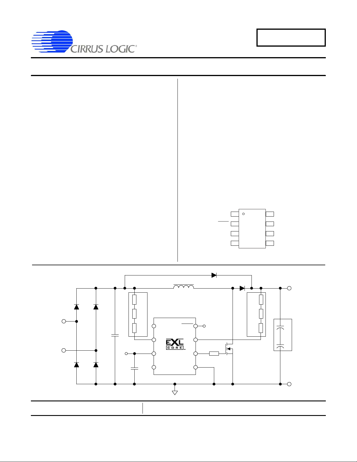
CS1600
8-lead SOIC
NC
STBY
IAC
FB
NC
VDD
GD
GND
1
2
3
4
8
7
6
5
D6
C1
D5
C2
BR1
BR1
BR1
BR1
AC
Mains
+12V
L1
Q1
R3
CS1600
IAC
NC
FB
STBY
VDD
GND
NC
GD
2
3
1
7
8
6
4
5
R1a
R1b
R2b
R2a
C3a
C3b
R2c
R1c
R
AC
R
FB
C
link
Low-cost PFC Controller for Electronic Ballasts
Features & Description
Lowest PFC System Cost for Electronic Ballasts
Variable Frequency Discontinuous Conduction Mode
Improved Efficiency Due to Variable Switching Frequency
EMI Signature Reduction from Digital Noise Shaping
Integrated Feedback Compensation
Overvoltage Protection with Hysteresis
Overpower Protection with Shutdown
UVLO with Wide Hysteresis
Thermal Shutdown with Hysteresis
Description
CS1600 is a high-performance Variable Frequency Discontinuous Conduction Mode (VF - DCM), active Power Factor
Correction (PFC) controller, optimized to deliver the lowe st PFC
system cost for electronic ballast applications.
A variable ON time / variable frequency algorithm is used to
achieve near unity power factor. This algorithm spreads the EMI
frequency spectrum, which reduces the conducted EMI filtering
requirements. The feedback loop is closed through an integrated
compensation network within the IC, eliminating the need for
additional external components. Protection features such as
overvoltage, overcurrent, overpower, open- and short-circuit protection, overtemperature, and brownout help protect the device
during abnormal transient conditions.
Pin Assignments
Advance Product Information
Cirrus Logic, Inc.
http://www.cirrus.com
This document contains information for a product under development.
Cirrus Logic reserves the right to modify this product without notice.
Copyright Cirrus Logic, Inc. 2010
(All Rights Reserved)
JUN ‘10
DS904A6
Page 2
1. PIN DESCRIPTIONS
NC
STBY
IAC
FB
NC
VDD
GD
GND
1
2
3
4
8
7
6
5
CS1600
Table 1. Pin Descriptions
Pin Name Pin # I/O
NC
STBY
IAC
FB
GND
GD
VDD
1, 8 -
2IN
3IN
4IN
5–
6OUT
7IN
Description
No Connect — Connect these pins to VDD to prevent any leakage path that could
arise from leaving them unterminated.
Standby — This is an active-low pin. Shorting this pin to GND disables PFC switching. The input has a pull-up resistor and should be driven with an open-collector
device. Leave this pin unterminated when not in use.
Rectified Line Voltage Sense — The IAC pin is used to sense the rectified line voltage. This signal, in conjunction with the signal on the FB pin, is used in the Power
Factor Correction (PFC) algorithm
A filter capacitor of up to 2.2 nF may be added between this pin and VDD to provide
noise immunity.
Feedback Voltage Sense — The FB pin is used to sense the output voltage of the
PFC stage. This signal, in conjunction with the signal on the IAC pin, is used in the
Power Factor Correction (PFC) algorithm.
A filter capacitor of up to 2.2 nF may be added between this pin and VDD to provide
noise immunity.
Ground — GND is a common reference for all the functional blocks in this device.
Gate Drive — GD is the output of the device with a source capability of 0.5 A and a
current sink capacity of 1 A.
IC Supply Voltage — VDD is the input used to provide bias to the device. This pin
has an internal shunt to ground. An external bias needs to be applied for steadystate operation. A low-ESR ceramic decoupling capacitor at this pin is recommended
for reliable operation of this device.
2 DS904A6
Page 3
CS1600
2. CHARACTERISTICS AND SPECIFICATIONS
2.1 Absolute Maximum Ratings
Pin Symbol Parameter Value Unit
7
2,3,4 V
3,4 I
V
DD
IN
IC Supply Voltage
Input Voltage -0.5 to V
IN
Input Current 50 mA
1
6VGDGate Drive Voltage -0.3 to V
6I
GD
Gate Drive Current -1.0 / +0.5 A
1,2,3,4,5,6,8 ESD Human Body Model 2000 V
1,2,3,4,5,6,8 ESD Machine Model 200 V
1,2,3,4,5,6,8 ESD Charged Device Model 500 V
-P
-T
-T
Stg
D
Total Power Dissipation at 50° C
Junction Temperature Operating Range -40 to +125 ºC
J
Storage Temperature Range -65 to +150 ºC
2
Notes: 1. The CS1600 has an internal shunt regulator that controls the nominal operating voltage on the VDD pin.
2. Long term operation at the maximum junction temperature will result in reduced product life. Derate internal power
dissipation at the rate of 50 mW / ºC for variation over temperature.
V
z
DD
DD
600 mW
V
V
V
2.2 Electrical Characteristics
Recommended operating conditions (unless otherwise specified): TA = TJ = -40º to +125º C, VDD = 10 to 15 V, GND = 0 V.
Typical values are at T
Parameter Condition Symbol Min Typ Max Unit
Supply Voltage
V
DD
Turn-on Threshold Voltage
V
DD
V
Turn-off Threshold Voltage
DD
UVLO Hysteresis V
Zener Voltage
Supply Current Section
Start-up Supply Current V
Standby Supply Current STBY
Operating Supply Current C
PFC Gate Drive Section
Maximum Operating Frequency
Minimum Operating Frequency
Minimum Duty Cycle V
Maximum Duty Cycle
Minimum On Time VDD=13V t
Output Source Resistance I
Output Sink Resistance I
Rise Time C
= 25º C.
A
3,4
3,4
3,4
V
increasing V
DD
decreasing V
V
DD
=20mA V
I
DD
< V
DD
th(St)
< 0.8V I
= 1nF, fsw = 70 kHz I
L
Normal mode, VDD=13V f
Normal mode, VDD=13V f
= 13 V, STBY < 0.8 V t
DD
VDD=13V D
=100 mA, VDD=13V R
GD
=-200mA, VDD=13V R
GD
=1 nF, VDD=13V t
L
th(St)
th(Stp)
Hys
Z
I
ST
SB
DD
SW(max)
SW(min)
DC_min
max
on_min
OH
OL
r
8.4 8.8 9.3 V
7.1 7.4 7.9 V
-1.3-V
17.0 17.9 18.5 V
-6880μA
-80112μA
-1.71.9mA
62 66 70 kHz
20 22 23 kHz
--0%
64 66 68 %
0.45 0.5 0.55 μs
-9-Ω
-6-Ω
-3245ns
DS904A6 3
Page 4

Parameter Condition Symbol Min Typ Max Unit
Fall Time C
Output Voltage Low I
Output Voltage High I
=1 nF, VDD=13V t
L
GD =-200mA,VDD =13V V
GD =100mA,VDD =13V V
Feedback and Protection
Reference Current I
Overvoltage Protection Threshold I
Overvoltage Protection Current Hysteresis I
Undervoltage Protection Threshold
OVP/Iref
OVP(Hy)
I
UVP/Iref
OL
OH
ref
CS1600
f
-1525ns
-0.91.3v
11.3 11.8 - v
127 130 133 μA
105 107 110 %
-4-%
83 85 87 %
Undervoltage Protection Current Hysteresis I
3,4
3,4
% of full load as defined by Eq. 3
7
7
V
= 460V, GDRV turns off V
out
V
= 460V, GDRV turns on V
out
Overpower Protection Threshold
Overpower Protection Recovery
Input Brownout Protection Threshold
Input Brownout Recovery Threshold
UVP(Hy)
BP(th)
BR
-10-%
123 125 127 %
35 49 60 %
82 86 90 Vrms
94 97 100 Vrms
Thermal Protection
Thermal Shutdown Threshold
3
Thermal Shutdown Hysteresis T
T
SD
SD(Hy)
130 143 155 ºC
-9-ºC
STBY Input
Logic Threshold
5
Low
High
-
VDD – 0.8
-
-
0.8
-
2.3 Thermal Characteristics
Symbol Parameter Value Unit
θ
R
JA
Thermal Resistance (Junction to Ambient)6.
R
θ
JC
Thermal Resistance (Junction to Case)6.
3. Specifications guaranteed by design & characterization.
4. Specifications measured as an instantaneous quantity NOT as a time-averaged quantity.
5. STBY
is designed to be driven by an open-collector device. The input is internally pulled up with a 600 kΩ resistor.
6. The package thermal impedance is calculated in accordance with JESD 51.
7. For an output voltage, V
, other than 460V, the threshold scales by a factor of V
out
out
159 ºC / W
39 ºC / W
/460
V
4 DS904A6
Page 5
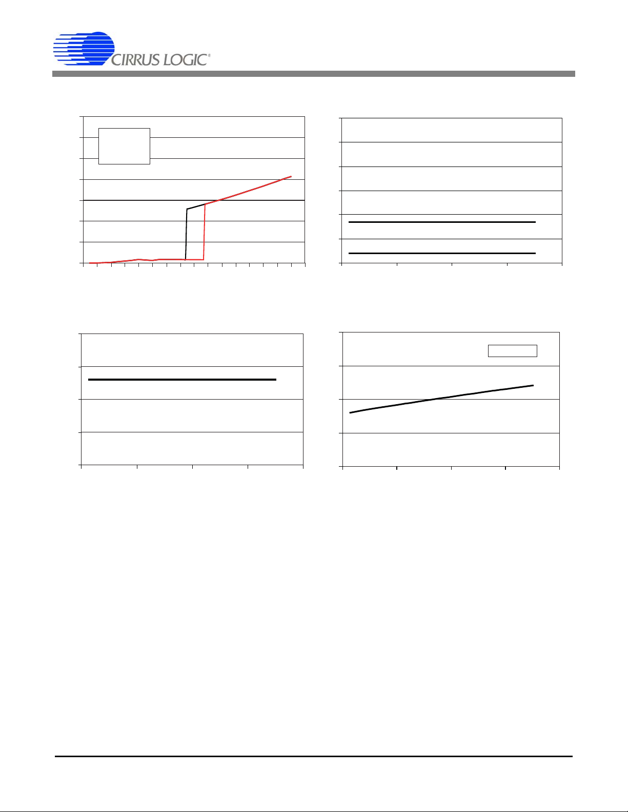
3. TYPICAL ELECTRICAL PERFORMANCE
0
0.5
1
1.5
2
2.5
3
3.5
0 1 2 3 4 5 6 7 8 9 10111213141516
VDD (V)
I
DD
(mA)
CL = 1 nF
f
SW
= 70 kHz
T
A
= 25 °C
Falling
Rising
7
8
9
10
11
12
13
-50 0 50 100 150
TEMP (oC)
V
DD
(V)
Startup
UVLO
Figure 2. Start-up & UVLO vs. Te mperat ure
Figure 3. UVLO Hysteresis vs. Temperature Figure 4. VDD Zener Voltage vs. TemperatureFigure 3. UVLO Hysteresis vs. Temperature
Figure 1. UVLO Characteristics
0
0.5
1
1.5
2
-50 0 50 100 150
TEMP (oC)
UVLO Hysteresis (V)
17
17.5
18
18.5
19
-50 0 50 100 150
TEMP (oC)
V
Z
(V)
IDD = 20 mA
CS1600
DS904A6 5
Page 6
CS1600
0
2
4
6
8
10
12
14
-60 -40 -20 0 40 100 120 140
Gate Resistor (ROH, ROL) Temp (oC)
Z
out
(Ohm)
Source
Sink
VDD = 13 V
I
source
= 100 mA
I
sink
= 200 mA
20 60 80
-50 0 50 100 150
TEM P (oC)
Supply Current (mA)
Start-up
Standby
0
0.2
0.4
0.6
0.8
1.0
1.2
1.4
1.6
1.8
Operating
VDD = 13 V
C
L
= 1 nF
f
SW
= 70 kHz
Start-up
Standby
Figure 5. Supply Current (ISB, IST, IDD) vs. T emperature Figure 6. Gate Resistance (ROH, ROL) vs. Temperature
6 DS904A6
Page 7

4. INTRODUCTION
Rectified Line Voltage Phase (Deg.)
% of Max
0 45 90 135 180
0
20
40
60
80
100
120
Line Voltage (% of Max)
Switching Frequency (% of Max)
CS1600
CS1600 is a digitally controlled Power Factor Correction
(PFC) controller that operates in the Variable Frequency
Discontinuous Conduction Mode (VF - DCM). The CS1600
uses a proprietary digital algorithm to optimize control of the
power switch to deliver highly efficient performance for
electronic ballast applications. With this control scheme, the
total number of external components needed is minimized in
comparison to conventional control techniques, thus reducing
the overall system cost.
Digital control is achieved by constantly monitoring two voltages
– the PFC output voltage (V
voltage (V
) at pin IAC. This is done by measuring the currents
rect
) at pin FB and the rectified AC line
link
that flow into the respective pins. These currents are then fed to
the inputs of two analog-to-digital converters (ADCs) and are
compared against an internal target current, I
.
ref
The digital outputs of the two ADCs are then processed in a
control algorithm which determines the behavior of the
CS1600 during start-up, normal operation, and under fault
conditions such as brownout, overvoltage, overcurrent,
overpower, and over-temperature. Details of operation during
these conditions are discussed in later sections of this
document.
Some of the key features of the CS1600 are as follows:
• Discontinuous Conduction Mode with Continuously
Variable Switching Frequency
The PFC switching frequency is varied every switching
cycle. This allows for a spread spectrum which minimizes
the conducted EMI peaks at any given frequency, thereby
minimizing the size and cost of the EMI filter required at
the front-end.
During start-up, the control algorithm limits the maximum
ON time and adjusts the frequency to avoid inductor saturation and provides a near-trapezoidal envelope for the
input current during every half cycle. During normal operation, as the line voltage changes over half of a line cycle,
the frequency varies approximately 2:1 as shown in
Figure 7 below.
Figure 7. Switching Frequency vs. Phase Angle
Maximum power transfer occurs at the peak of the AC line
voltage, at which time, the frequency reaches its maximum value. Switching losses are minimized during periods of low power transfer by switching at lower
frequencies near the zero-crossing of the AC line.
This switching frequency profile helps reduce total BOM
cost through savings in the size of the boost inductor and
the EMI filter components, while at the same time, improving overall system efficiency.
• Integrated Feedback Control
No external feedback compensation components are required for the CS1600. The internal digital control engine
self-compensates the feedback error signal using an
adaptive control algorithm.
• Protection Features
The CS1600 provides various protection features such as
undervoltage, overcurrent, overpower, open and short
circuit protection and brownout. It also provides the user
with the option of using the STBY
pin to disable switching
of the device.
DS904A6 7
Page 8

CS1600
PO [W]
f
SW
[kHz]
Max f
SW
50%
100
100%5%
Burst Mode
70
35
Min f
SW
PO [W]
f
SW
[kHz]
Max f
SW
50%
60
100%5%
Burst Mode
48
24
Min f
SW
DCM
Quasi
CRM
DCM
Quasi
CRM
DCM
I
LB
t [ms]
100%
90%
Startup Mode
Normal Mode
Startup Mode
Normal Mode
4.1 PFC Implementation
The PFC switching frequency profile over the line period has
been discussed in detail in Section 4. In addition, the dig ital
control algorithm tracks changes the AC input and operates in
different frequency bands at different line voltages as
illustrated in Figure 8 and Figure 9 below.
Figure 8. Switching Frequency vs. Output Power
< 165 VAC
V
in
Figure 9. Switching Frequency vs. Output Power
> 165 VAC
V
in
The CS1600 primarily operates in the DCM mode with a
properly sized inductor. However, it will move into a quasi-
CRM mode near the peaks of the input line, in order to enable
maximum power delivery, as illustrated in Figure 10 below.
Figure 10. DCM and quasi-CRM Operation with CS1600
4.1.1 Start-up Mode vs. Normal Mode
CS1600 operates in two discrete states:
Start-up mode:
When the output voltage of the PFC stage, V
nominal value, the device operates in the start-up mode. It
continues operating in this mode till the nominal V
is reached. The start-up algorithm provides an ON time which
is varied in proportion to the sensed rectified voltage, while
changing the switching frequency to provide maximum power.
During this start-up phase of operation, the switching
frequency could be significantly lower than the normal
operating frequency, and the input current waveform is forced
into following a trapezoidal envelope in phase with the line
voltage, to maximize energy transfer. The ON time and the
switching frequency of the IC ensure that peak currents are
kept controlled to prevent saturation of the boost inductor
during this period.
Normal mode:
Once V
reaches its nominal value, the chip operates in the
link
normal mode. Here, the frequency follows the profile shown in
Figure 7, and the ON time is varied to achieve PFC. Any drop
to below its undervoltage threshold, as defined in
in V
link
Section 2.2. Electrical Characteristics re-triggers the start-up
mode of operation. A simplified illustration of operation in
these two modes is shown below in Figure 11.
, is <90% of its
link
voltage
link
8 DS904A6
Figure 11. Start-up and Normal Modes
Page 9
4.1.2 Burst Mode
V
in
[V]
t [ms]
FET V
gs
Burst Mode
Active
V
in
P
O
[W]
t [ms]
5%
PFC
Disable
R
FB
V
linkVDD
–
I
ref
-----------------------------
=
[Eq.1]
R
AC
RFB=
[Eq.2]
R
FB
I
FB
FB
VDD
ADC
7
R
IFB
15k
4
V
link
R
FB
I
FB
FB
VDD
ADC
7
R
IFB
15k
4
V
link
T
on
0.001126
V
rect
------------------------ -
≤
In addition to the start-up mode and normal mode of operation,
the controller enters the burst mode of operation when the
estimated output power (P
During this stage, the PFC driver is disabled intermittently over
a full line cycle period, as shown in Figure 12. The period of
time for which the PFC drive is disabled depends on the level
of loading present..
) is < 5% of its nominal value.
O
I
= Target Reference current used for feedback
ref
Figure 13. Output Feedback
CS1600
Figure 12. Burst Mode of Operation
4.2 Input Feedforward and Output
Figure 14. Input Feedforward
Regulation
The CS1600 continuously monitors the rectified AC line and
the PFC output voltage through sense resistors tied to the IAC
and the FB pins to monitor the voltages, scaled as currents.
The rectified AC line sense resistor R
size of the resistor R
used for current feedback from the
FB
needs to be the same
AC
PFC output voltage. These currents are effectively compared
against an internal reference current to provide adaptive PFC
control. The resistor values are calculated as follows:
where
R
= Feedback resistor used to sense the PFC output
FB
voltage
RAC = Feedforward resistor used to sense the rectified line
voltage
V
= PFC Output Voltage
link
V
= IC Supply Voltage
DD
DS904A6 9
4.3 Protection Features
4.3.1 Overvoltage Protection
If the PFC output voltage, V
threshold, as scaled by the current monitored by the sense
resistors, the CS1600 provides protection by disabling the
gate drive. A nominal hysteresis is provided to allow the
system to recover from the fault condition, before switching is
resumed.
4.3.2 Overcurrent Protection
The CS1600’s digital controller algorithm limits the ON
time of the Power MOSFET by the following equation:
Where T
turned on and V
event of a sudden line surge or sporadic, high dv/dt line
voltages, this equation may not limit the ON time appropriately. For this type of line disturbance, additional protection mechanisms, such as fusible resistors, fast-blow
fuses, or other current-limiting devices, are recommended.
is the max time that the power MOSFET is
on
is the rectified line voltage. In the
rect
, exceeds the overvoltage
link
Page 10

CS1600
P
o
αη
V
in min()
()×2×
V
link
V
in min()
2×()–
2f
maxLBVlink
×××
---------------------------------------------------------
×=
[Eq.3]
α
V
link
400V
------------- -
90V
V
in min()
--------------------
×
2
V
link
V
link
400V
------------- -
90V× 2×
–
V
link
V
in min()
2×–
-------------------------------------------------------------------- -
×=
56 ms
56 ms
Start
Timer
Enter Standby Exit Standby
Upper
Lower
Brownout
Thresholds
Start Timer
T
Brownout
<1 nF
600 kΩ
See Text
CAP
STBY
GND
CS1600
4.3.3 Overpower Protection
The nominal output power is estimated internally by the
CS1600 from the following equation
where
Po = rated output power of the system
η = efficiency of the boost converter = estimated as 100% by
the internal PFC algorithm
V
= minimum RMS line voltage for operation
in(min)
= PFC output voltage
V
link
f
= maximum switching frequency
max
L
= boost inductor used in the application
B
Operation estimated to be at power levels higher than that
calculated by Eq. 3 above is tracked by the IC as an
overpower condition. During this phase, the PFC output
voltage, V
power draw increases. When V
, is reduced and will continue to decrease as the
link
reaches its undervoltage
link
threshold, it goes into the start-up mode as explained in
section 4.1.1.
At this point, the overpower protection timer is activated. If this
condition continues to exist for 112 ms, the gate drive is
disabled for a period of about 3 seconds. This “hiccup” mod e
of operation continues until the fault is removed.
If a value of the boost inductor other than that obtained from
Eq. 3 above is used, the total output power capability as well
as the thresholds for the different operating conditions will
scale accordingly.
4.3.4 Open/short circuit protection
The CS1600 protects the system in case the feedforward
resistor tied to the IAC pin or the feedback resistor tied to the
FB pin is open or shorted to ground.
A fault seen on the resistor going into the FB pin would i mply
no current being fed into the pin, which would trigger the V
undervoltage algorithm as described in Section 4.3.1.
A fault detected on the IAC pin would trigger the brownout
condition discussed in Section 4.3.5 below.
link
for the output voltage, drops to 49% of its nominal value.
Detection of brownout for a period of 56 ms disables the gate
drive. The device continues to monitor the input voltage while
in this condition. The CS1600 exits the brownout mode when
the input current scales up to, and stays above 56.4% of its
nominal value for a period of 56 ms.
To minimize false detects, the brownout detection circuit
increases the brownout detection time by a factor of 1.6 mS/V
for every volt differential between the minimum operating
voltage and the brownout threshold, following half of a line
cycle of exceeding the brownout threshold. The following
diagram illustrates the brownout sequence whereby the
CS1600 enters standby, and upon recovery from brownout,
enters normal operation..
Figure 15. Brownout
4.3.6 Over-temperature Protection
Over-temperature protection is activated and PFC switching is
disabled when the die temperature of the device exceeds
125°C. There is a hysteresis of about 30°C before resumption
of normal operation.
4.4 Standby (STBY) Function
The standby (STBY) pin may be used as a means to force the
CS1600 into a non-operating, low-power state. The STBY
input should be driven by an open-collector/open-drain
device. Internal to the pin, there is a pull-up resistor connected
to the VDD pin as shown in Figure 16. A filter capacitance of
about 1000 pF is recommended while this pin is being used.
4.3.5 Brownout Protection
Brownout occurs when the current representing the rectified
input voltage, nominally 100% of the reference current used
10 DS904A6
Figure 16. STBY
Pin Connection
Page 11
CS1600
D6
C1
D5
C2
BR1
BR1
BR1
BR1
AC
Mains
+12V
L1
Q1
R3
CS1600
IAC
NC
FB
STBY
VDD
GND
NC
GD
2
3
1
7
8
6
4
5
R1a
R1b
R2b
R2a
C3a
C3b
R2c
R1c
R
AC
R
FB
C
link
Figure 17. CS1600 Basic Application Circuit
R
FB
V
linkVdd
–
I
ref
--------------------------- -
=
R
FB
460 12–
130 10
6–
×
--------------------------- -
=
R
FB
3.45MΩ=
[Eq.4]
R
ACRFB
=
R
AC
3.45MΩ=
[Eq.5]
5. FLUORESCENT BALLAST APPLICATION EXAMPLE
The following section gives an example for a front-end PFC stage design for an electronic ballast application. The equations that
follow may be used as guidelines for any other requirements using the CS1600.
5.1 Component Selection Guidelines
The following design example is for a wide-input-voltage
fluorescent ballast application using 2 T5 lamps in series for a
total nominal power of 108W.The target specifications for the
PFC portion of the design, assuming a 94% efficient second
stage, are as follows:
V
in(min)
V
in(max)
V
P
link
o
108 VAC
305 VAC
460 V
115 W
η 95%
5.1.1 IAC and IFB Sense Resistors
The rectified line voltage, VAC, and the output voltage of the
PFC boost converter, V
sense resistors, whose values are estimated based on the
equations below:
DS904A6 11
, are scaled as currents by using
link
where
= Feedback resistor used to reflect the PFC output
R
FB
voltage
R
= Feedforward resistor used to reflect the rectified line
AC
voltage
V
= PFC Output Voltage
link
V
= IC Supply Voltage
DD
I
= Target reference current used for feedback
ref
1% or lower tolerance resistors are recommended to
maximize the tightly toleranced system behavior provided by
the unique digital controller in the CS1600. Resistors may be
separated into two or more series elements if voltage
breakdown and/or regulatory compliance is of concern.
5.1.2 PFC Input Filter Capacitor
For a typical 115 W PFC output stage required to pow er up a
108 W fluorescent ballast, an input filter capacitance of
0.33 μF is recommended. Capacitor tolerances and the value
of the EMI filter capacitor need to be considered when
selecting the value of the capacitor to be used in this
application.
Page 12

CS1600
α
V
link
400V
------------- -
90V
V
in min()
--------------------
×
2
V
link
V
link
400V
------------- -
90V× 2×
–
V
link
V
in min()
2×–
-------------------------------------------------------------------- -
×=
[Eq.6]
α
V
link
400V
------------- -
90V
V
in min()
--------------------
×
2
V
link
V
link
400V
------------- -
90V× 2×
–
V
link
V
in min()
2×–
-------------------------------------------------------------------- -
× 0.937==
L
B
αη
V
in min()
()
2
××
V
link
V
in min()
2×()–
2f
maxPOVlink
×××
---------------------------------------------------------
×=
[Eq.6]
LB0.937 0.95 108×
2
×
460 108 2×–()
27010
3
× 115 460×××
----------------------------------------------------------------
× 431μH==
I
LB rms()
P
O
V
in min()
2×η×
------------------------------------------- -
β×=
I
LB rms()
1.07A=
I
LB rms()
115
1082× 0.95×
-----------------------------------------
1.35×=
[Eq.7]
I
LB pk()
4 P
O
×
η V×
in min()
2×
------------------------------------------- -
=
I
LB pk()
3.17 A=
I
LB pk()
4 115×
0.95 108× 2×
-----------------------------------------
=
[Eq.8]
I
FET rms()
P
O
V
in min()
2×η×
------------------------------------------- -
γ×=
I
LB rms()
0.91A=
I
LB rms()
115
1082× 0.95×
-----------------------------------------
1.15×=
[Eq.9]
I
Dpk()ILB pk()
=
I
Dpk()
3.17 A=
[Eq.10]
I
Davg()
P
O
V
link
----------- -
=
I
Davg()
0.25A=
I
Davg()
115
460
--------- -
=
[Eq.11]
[Eq.12]
C
out
P
O
2π f
line min()
× V
link
×ΔV
link rip()
×
-------------------------------------------------------------------------------------- -
=
5.1.3 PFC Boost Inductor
Equation 3 can be rewritten to calculate the PFC boost
Inductor, L
The RMS current rating for the inductor is estimated using an
scaling factor used to account for variations in the input
current shape across the AC line cycle, over and above the
nominally calculated value. The nominal value before using
the scaling factor is as follows:
, as follows:
B
5.1.4 PFC MOSFET
The peak voltage stress on the PFC MOSFET is a diode drop
above the output voltage. Accounting for leakage spikes, for
the 460 V output application, a 600 V FET is recommended.
The FET should be able to handle the same peak current as
that seen through the inductor. This would amount to 3.96 A.
The scaling factor to determine the RMS current through the
MOSFET for a 108 V input is about 1.15, and the minimum
RMS current rating, I
, required for the FET is
FET(rms)
calculated as follows:
where
γ = FET scaling factor
5.1.5 PFC Diode
The PFC diode peak current is equal to the inductor peak
current:
where
β = inductor scaling factor
The peak inductor current, I
following equation:
Inductor tolerances should be considered when estimating the
peak currents present in the application.
The internal control algorithm of the controller dictates that the
peak inductor current seen in the application could be as high
as a pre-defined threshold of 0.001984 time s the inverse of
the inductor, which in this example amounts to 4.72 A. Care
needs to be taken to ensure that the saturation current rating
of the PFC boost inductor factors in this threshold used for the
protection schemes.
For a 40 V ripple and minimum line frequency of 45 Hz, the
12 DS904A6
, may be estimated using the
LB(pk)
The PFC diode average current is calculated as follows:
5.1.6 PFC Output Capacitor
The output capacitor needs to be designed to meet the voltage
ripple and hold-up time requirements. In the case of a costsensitive ballast application, the hold-up requirement is not a
key requirement.
To address the output ripple requirements, the following
equation may be used as a guide:
where
= Output Capacitance value
C
out
P
= Output Power
o
f
line(min)
V
ΔV
= Minimum Line Frequency
= PFC Output Voltage
link
= Peak-Peak Voltage Ripple on the PFC Output
link
Page 13

CS1600
C
out
115
2π 45× 460× 40×
------------------------------------------------ -
22.1μF==
output capacitance needed is calculated as: The voltage rating on the capacitor needs to account for the
operation of the device before it hits the overvoltage protection
threshold. This is typically 105% of nominal value, which is
483 V. With the ripple voltage factored in, 22 μF of
capacitance rated at 500 V would suffice for this application.
DS904A6 13
Page 14

5.2 Bill of Materials (for Application Example shown in Figure 17)
Designator Value Description/Part Number
R1a 1.5 MΩ
R1b 1.5 MΩ
R1c 1.5 MΩ
R2a 1.5 MΩ
R2b 1.5 MΩ
R2c 1.5 MΩ
R3 24.9Ω
C1 0.47μF
C2 4.7μF
C3a
C3b
BR1 4A, 600V Bridge diode - GBU4J-BP
D5 1 A, 600 1N4005
D6 3A, 600V MURS360
L1 360μH (max) TBD (Premier Magnetics)
Q1 9A, 600V FCP9N60N
CS1600 - CS1600-FSZ
23.5μF2 47μF, 250V caps in series
CS1600
14 DS904A6
Page 15

5.3 Summary of Equations
R
FB
V
linkVDD
–
I
ref
-----------------------------
=
R
AC
RFB=
P
O
αη
V
in min()
()×
2
×
V
link
V
in min()
2×()–
2f
maxLBVlink
×××
---------------------------------------------------------
×=
I
LB rms()
P
O
V
in min()
2×η×
------------------------------------------- -
β×=
I
LB pk()
4P
O
×
η V×
in min()
2×
------------------------------------------- -
=
I
FET rms()
P
O
V
in min()
2×η×
------------------------------------------- -
γ×=
I
Dpk()ILB pk()
=
I
Davg()
P
O
V
link
----------- -
=
C
out
P
O
2π f
line min()
× V
link
×ΔV
link rip()
×
-------------------------------------------------------------------------------------- -
=
Eq. # Equation
1, 4
2, 5
3, 6
7
CS1600
8
9
10
11
12
DS904A6 15
Page 16
6. PACKAGE DRAWING
8L SOIC (150 MIL BODY) PACKAGE DRAWING
D
H
E
e
b
A1
A
c
L
∝
SEATING
PLANE
1
CS1600
DIM MIN MAX MIN MAX
INCHES MILLIMETERS
A 0.053 0.069 1.35 1.75
A1 0.004 0.010 0.10 0.25
B 0.013 0.020 0.33 0.51
C 0.007 0.010 0.19 0.25
D 0.189 0.197 4.80 5.00
E 0.150 0.157 3.80 4.00
e 0.040 0.060 1.02 1.52
H 0.228 0.244 5.80 6.20
L 0.016 0.050 0.40 1.27
∝
0° 8° 0° 8°
JEDEC # : MS-012
16 DS904A6
Page 17

CS1600
7. ORDERING INFORMATION
Part # Temperature Range Package Description
CS1600-FSZ -40 °C to +125 °C 8-lead SOIC, Lead (Pb) Free
8. ENVIRONMENTAL, MANUFACTURING, & HANDLING INFORMATION
Model Number Peak Reflow Temp MSL Rating
CS1600-FSZ 260 °C 2 365 Days
a. MSL (Moisture Sensitivity Level) as specified by IPC/JEDEC J-STD-020.
b. Stored at 30 °C, 60% relative humidity.
a
Max Floor Life
b
DS904A6 17
Page 18

9. REVISION HISTORY
Contacting Cirrus Logic Support
For all product questions and inquiries contact a Cirrus Logic Sales Representative.
To find one nearest you go to http://www.cirrus.com
IMPORTANT NOTICE
“Advance” product information describes products that are in development and subject to development changes.
Cirrus Logic, Inc. and its subsidiaries (“Cirrus”) believe that the information contained in this document is accurate and reliable. However, the information is subject
to change without notice and is provided “AS IS” without warranty of any kind (express or implied). Customers are advised to obtain the latest version of relevant
information to verify, before placing orders, that information being relied on is current and complete. All products are sold subject to the terms and conditions of sale
supplied at the time of order acknowle dgment, including tho se pertaining to wa rranty, indemnification, an d limitation of liability. No responsibility is assumed by Cirrus
for the use of this information, including use of this inform ation a s the basis for m anufactur e or sale of an y items, or for i nfringement of patents or other rights of third
parties. This document is the property of Cirrus and by furnishing this information, Cirrus grants no license, express or implied under any patents, mask work rights,
copyrights, trademarks, trade secrets or other intellectual pro perty rights. Cirrus owns the copyr ights associated with the information con tained here in and gives consent for copies to be made of the information only for use within your organization with respect to Cirrus inte grated circuits or other products of Cirrus. This consent
does not extend to other copying such as copying for general distribution, advertising or promotional purposes, or for creating any work for resale.
CERTAIN APPLICATIONS USING SEMICONDUCTOR PRODUCTS MAY INVOLVE POTENTIAL RISKS OF DEATH, PERSONAL INJURY, OR SEVERE PROPERTY OR ENVIRONMENTAL DAMAGE (“CRITICAL APPLICATIONS”). CIRRUS PRODUCTS ARE NOT DESIGNED, AUTHORIZED OR WARRANTED FOR USE
IN PRODUCTS SURGICALLY IMPLANTED INTO THE BODY, AUTOMOTIVE SAFETY OR SECU RITY DEVICES, LIFE SUPPOR T PRODUCTS OR OTHE R CRITICAL APPLICATIONS. INCLUSION OF CIRRUS PRODUCTS IN SUCH APPLICATIONS IS UNDERSTOOD TO BE FULLY AT THE CUSTOMER'S RISK AND CIRRUS DISCLAIMS AND MAKES NO WARRANTY, EXPRESS, STATUTORY OR IMPLIED, INCLUDING THE IMPLIED WARRANTIES OF MERCHANTABILITY AND
FITNESS FOR PARTICULAR PURPOSE, WITH REGARD TO ANY CIRRUS PRODUCT THAT IS USED IN SUCH A MANNER. IF THE CUSTOMER OR CUSTOMER'S CUSTOMER USES OR PERMITS THE USE OF CIRRUS PRODUCTS IN CRITICAL APPLICATIONS, CUSTOMER AGREES, BY SUCH USE, T O FULLY
INDEMNIFY CIRRUS, ITS OFFICERS, DIRECTORS, EMPLOYEES, DISTRIBUTORS AND OTHER AGENTS FROM ANY AND ALL LIABILITY, INCLUDING ATTORNEYS' FEES AND COSTS, THAT MAY RESULT FROM OR ARISE IN CONNECTION WITH THESE USES.
Cirrus Logic, Cirrus, and the Cirrus Logic logo designs are trade m ar ks of Cirr us Lo gi c, Inc. All othe r br an d an d pr od uct na m e s in this document may be trademarks
or service marks of their respective owners.
Revision Date Changes
A1 OCT 2009 Initial Advance Information release.
CS1600
A2 MAR 2010
Revised feature list, product description and p arametric table to r eflect
the C0 version of silicon.
A3 MAR 2010
Revised to reflect the update in switching frequency and variation of
frequency over line.
A4 APR 2010
Revised parametric table and equations to reflect the C1 version of
silicon.
A5 MAY 2010 Updated with additional test bench da ta for EP level.
A6 JUN 2010 Added
Rθ
JA and RθJC
in electrical specifications section.
18 DS904A6
 Loading...