

Page 1
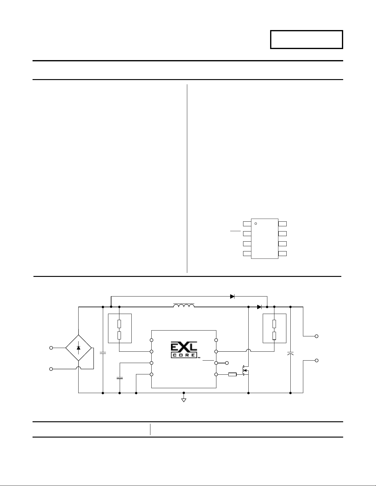
NC
STBY
IAC
FB
NC
VDD
GD
GND
1
2
3
4
8
7
6
5
8-lead SOIC
D2
C1
D1
CS1500
C2
L
B
C3
Q1
6
2
8
5
7
3
1
R1a
R1b
R2a
R2b
R3
FB
GD
NC
STBY
GND
VDD
IAC
NC
R
AC
R
FB
BR1
AC
Mains
Regulated
DC Outp u t
4
May ?$shortyear>
CONFIDENTIAL
Digital Power Factor Correction IC
CS1500
Features & Description
Digital EMI Noise Shaping
Excellent Efficiency Under All Load Conditions
Minimal External Devices Required
Optimized Digital Loop Compensation
Comprehensive Safety Features
• Undervoltage Lockout (UVLO)
• Output Overvoltage Protection
• Input Current Limiting
• Output Overpower Protection
• Input Brownout Protection
• Open/short Loop Protection for IAC & FB Pins
• Thermal Shutdown
Description
The CS1500 is a high-performance power factor correction (PFC)
controller for universal AC input, which uses a proprietary digital
algorithm for discontinuous conduction mode (DCM) with variable
on-time and variable frequency control, ensuring unity power factor.
The CS1500 incorporates all the safety features necessary for
robust and compact PFC stages. In addition, it has burst mode
control to lower the light-load/standby losses to a minimum.
Protection features such as overvoltage, overcurrent, overpower,
open- and short-circuit protection, overtemperature, and brownout
help protect the device during abnormal transient conditions.
The digital controller optimizes the system stability and transient
performance, simplifies the PFC design, reduces the external
component count and BOM costs. The simple design and
minimum cost makes CS1500 the ideal choice for PFC up to 300
watts.
Pin Assignments
Advance Product Information
Cirrus Logic, Inc.
http://www.cirrus.com
This document contains information for a product under development.
Cirrus Logic reserves the right to modify this product without notice.
Copyright Cirrus Logic, Inc. 2010
(All Rights Reserved)
MAY ‘10
DS849A6
Page 2

May ?$shortyear>
CONFIDENTIAL
Table 1. Pin Descriptions
CS1500
Pin Name Pin # I/O
NC
STBY
1, 8 -
2IN
IAC
FB
GND
GD
3IN
4IN
5-
6OUT
VDD
7IN
Description
NC — No connections
Remote On/Off Control — A voltage below 0.8 V shuts down the IC (not latched) and
brings the device into low power consumption mode. The input has an internal 600 kΩ
pull-up resistor to the VDD pin and should be driven with an open-collector device.
Rectifier Voltage Sense — A current proportional to the rectified line voltage (V
fed into this pin. The current is measured with an A/D converter.
Link Voltage Sense — A current proportional to the output link voltage (V
PFC is fed into this pin. The current is measured with an A/D converter.
Ground — Current return for both the input signal portion of the IC and the gate driver.
Gate Driver Output — The totem pole stage is able to drive the power MOSFET with a
peak current of 0.5 A source and 1.0 A sink. The high-level voltage of this pin is
clamped at V
IC Supply Voltage — Supply voltage of both the input signal portion of the IC and the
gate driver.
to avoid excessive gate voltages.
Z
link
rect
) of the
) is
2 DS849A6
Page 3
May ?$shortyear>
CONFIDENTIAL
1. CHARACTERISTICS AND SPECIFICATIONS
1.1 Absolute Maximum Ratings
Pin Symbol Parameter Value Unit
7V
DD
1,2,3,4,8 - Analog Input Maximum Voltage -0.5 to V
3,4 - Analog Input Maximum Current 50 mA
6V
GD
6IGDGate Drive Output Current -1.0 / +0.5 A
-P
- θ
T
-T
-T
Stg
IC Supply Voltage V
Z
Gate Drive Output Voltage -0.3 to V
Total Power Dissipation @ TA=50° C 600 mW
D
Junction-to-Ambient Thermal Impedance 107 ºC / W
JA
A
Operating Ambient Temperature Range
Junction Temperature Operating Range -40 to +125 ºC
J
1
-40 to +125 ºC
Storage Temperature Range -65 to +150 ºC
CS1500
Z
Z
V
V
V
1.2 Electrical Characteristics
(TA = 25º C, VDD = 13V, -40º < TJ < +125º C, CL=1nF between pin GD and GND, all voltages are measured with respect to
GND; all current are positive when flowing into the IC; unless otherwise specified). Recommended V
Parameter Condition Symbol Min Typ Max Unit
VDD Supply Voltage
Turn-on Threshold Voltage V
Turn-off Threshold Voltage (UVLO) V
Increasing V
DD
Decreasing V
DD
UVLO Hysteresis V
Zener Voltage I
=20mA V
DD
DD(on)
DD(off)
Hys
Z
8.4 8.8 9.3 V
7.1 7.4 7.9 V
-1.3-V
17.0 17.9 18.5 V
VDD Supply Current
Start-up Supply Current V
DD=VDD(on)
Standby Supply Current STBY
Operating Supply Current C
=1nF, fsw=70kHz I
L
<0.8V I
I
ST
SB
DD
-6880μA
-80112μA
-1.71.9mA
PFC Gate Drive
Maximum Operating Frequency
Minimum Operating Frequency
Maximum Duty Cycle
6
6
6
Output Source Resistance I
Output Sink Resistance I
Rising Time C
Falling Time C
Output Voltage Low State I
Output Voltage High State I
VDD = 13V f
VDD = 13V f
VDD = 13V D
=100mA,VDD = 13V R
GD
= -200mA,VDD = 13V R
GD
=1nF,VDD = 13V t
L
=1nF,VDD = 13V t
L
= -200mA,VDD = 13V Vol - 0.9 1.3 V
GD
=100mA,VDD = 13V Voh 11.3 11.8 - V
GD
SW(max)
SW(min)
max
OH
OL
r
f
62 66 70 kHz
20 22 23 kHz
64 66 68 %
-9-Ω
-6-Ω
-3245ns
-1525ns
= 10 – 15 V.
DD
DS849A6 3
Page 4
May ?$shortyear>
CONFIDENTIAL
Parameter Condition Symbol Min Typ Max Unit
Feedback & Protection
Reference Current I
Output Voltage at Startup Mode 25º C, 115 VAC V
Output Voltage at Normal Mode V
Overvoltage Protection Threshold 25º C, 115 VAC V
Overvoltage Protection Hysteresis V
Overpower Protection Threshold
Overpower Protection Recovery
Input Brownout Protection Threshold 25º C, GDRV turns off V
Input Brownout Recovery Threshold 25º C, GDRV turns on V
Thermal Protection
Thermal Shutdown Threshold T
Thermal Shutdown Hysteresis T
STBY Input
5
Logic Threshold Low - - 0.8 V
Logic Threshold High Vdd-0.8 - - V
2,3
REF
O(startup)
O(nom)
OVP
OVP(Hy)
2,4
2,4
1
25º C, 115 VAC - 125 - %
25º C, 115 VAC - 100 - %
BP(th)
BR
SD
SD(Hy)
-129-μA
-360-V
-400-V
415 418 421 V
-4-V
62 65 68 Vrms
77 80 83 Vrms
130 143 155 ºC
-9-ºC
CS1500
NOTES:
1. Specifications guaranteed by design & characterization and correlation with statistical process controls.
2. Specification are based upon a PFC system configured for AC input of 90-265 VAC (Sine), 45/65 Hz, V
R
=3x1.0 MΩ, RFB=3x1.0 MΩ, C3 = 180 μF, LB= 360 μH, 90 W. For othe r V
AC
Application Example.
3. Detailed Calculation See Section 4 Application Example.
4. Overpower protection is scaled to rated power.
5. STBY
is designed to be driven by an open collector. The input is internally pulled up with a 600 kΩ resistor.
6. Normal operation mode, see Section 3.2.
voltages, refer to Section 4
link
=400V,
link
4 DS849A6
Page 5
May ?$shortyear>
0
0.5
1
1.5
2
2.5
3
3.5
0 1 2 3 4 5 6 7 8 9 10111213 141516
VDD (V)
I
DD
(mA)
CL = 1 nF
f
SW
= 70 kHz
T
A
= 25 °C
Falling
Rising
7
8
9
10
11
12
13
-50 0 50 100 150
TEMP (oC)
V
DD
(V)
Startup
UVLO
0
0.5
1
1.5
2
-50 0 50 100 150
TEMP (oC)
UVLO Hysteresis (V)
17
17.5
18
18.5
19
-50 0 50 100 150
TEMP (oC)
V
Z
(V)
IDD = 20 mA
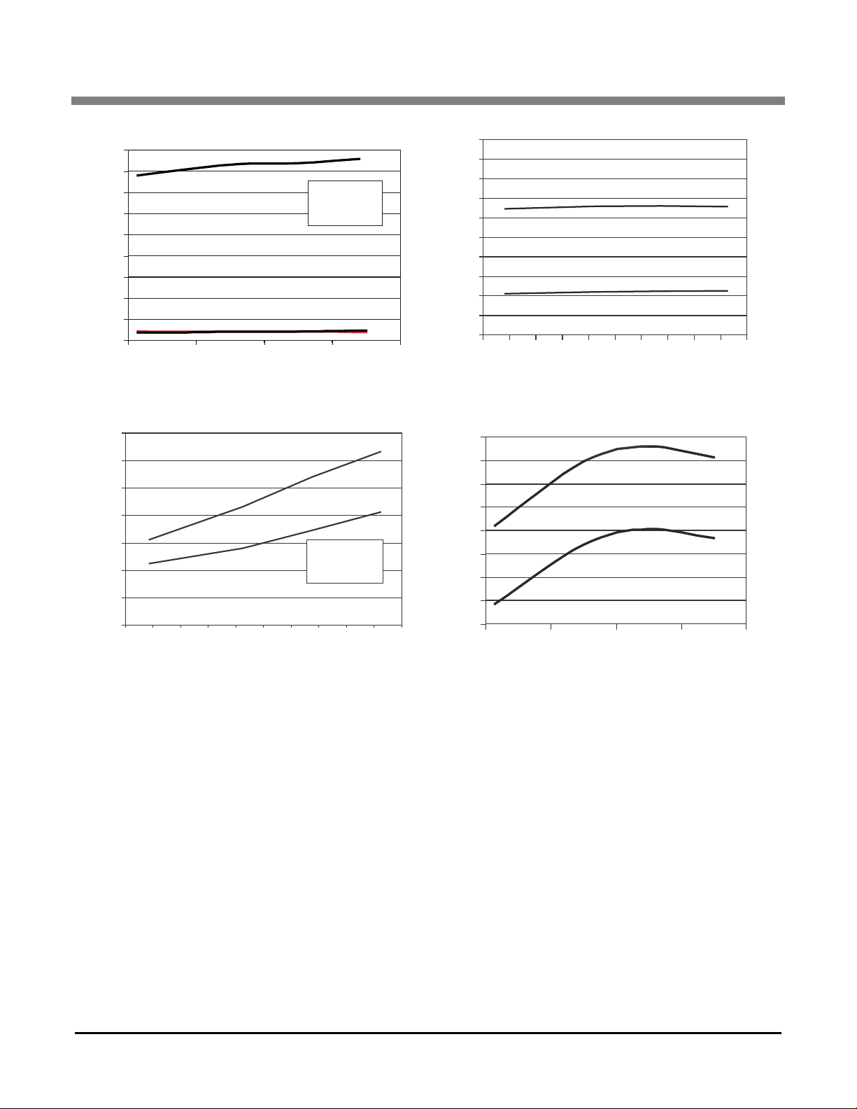
Figure 1. Supply Current vs. Supply Voltage Figure 2. Start-up & UVLO vs. Temp
Figure 3. UVLO Hysteresis vs. Temp Figure 4. VDD Zener Voltage vs. Temp
CONFIDENTIAL
2. TYPICAL ELECTRICAL PERFORMANCE
CS1500
DS849A6 5
Page 6
May ?$shortyear>
385
390
395
400
405
410
415
420
425
-50 0 50 100 150
Temperature (°C)
V
link
(V)
OVP
Normal
Frequency (kHz)
Min Freq
Max Freq
TEMP (oC)
0
10
20
30
40
50
60
70
80
90
100
-60 -40 -20 0 20 40 60 80 100 120 140
0
2
4
6
8
10
12
14
-60 -40 -20 0 40 100 120 140
Gate Resistor (ROH, ROL) Temp (oC)
Z
out
(Ohm)
Source
Sink
VDD = 13 V
I
source
= 100 mA
I
sink
= 200 mA
20 60 80
-50 0 50 100 150
TEM P (oC)
Supply Current (mA)
Start-up
Standby
0
0.2
0.4
0.6
0.8
1.0
1.2
1.4
1.6
1.8
Operating
VDD = 13 V
C
L
= 1 nF
f
SW
= 70 kHz
Start-up
Standby
Figure 5. Supply Current (ISB, IST, IDD) vs. Temp Figure 6. Min/Max Operating Frequency vs. Temp
Figu r e 7 . Gate Resistance (R
OH
, ROL) vs. Temp Figure 8. OVP vs. Temp
CONFIDENTIAL
CS1500
6 DS849A6
Page 7
IAC
FB
STBY
3
4
2
CS1500
GD
6
VDD
7
NC
8
GND
5
Processor
Logic
NC
1
PWM
Driver
Oscillator
Protection
ADC
T
on
0.001126
V
rect
------------------------ -
≤
May ?$shortyear>
CONFIDENTIAL
3. INTRODUCTION
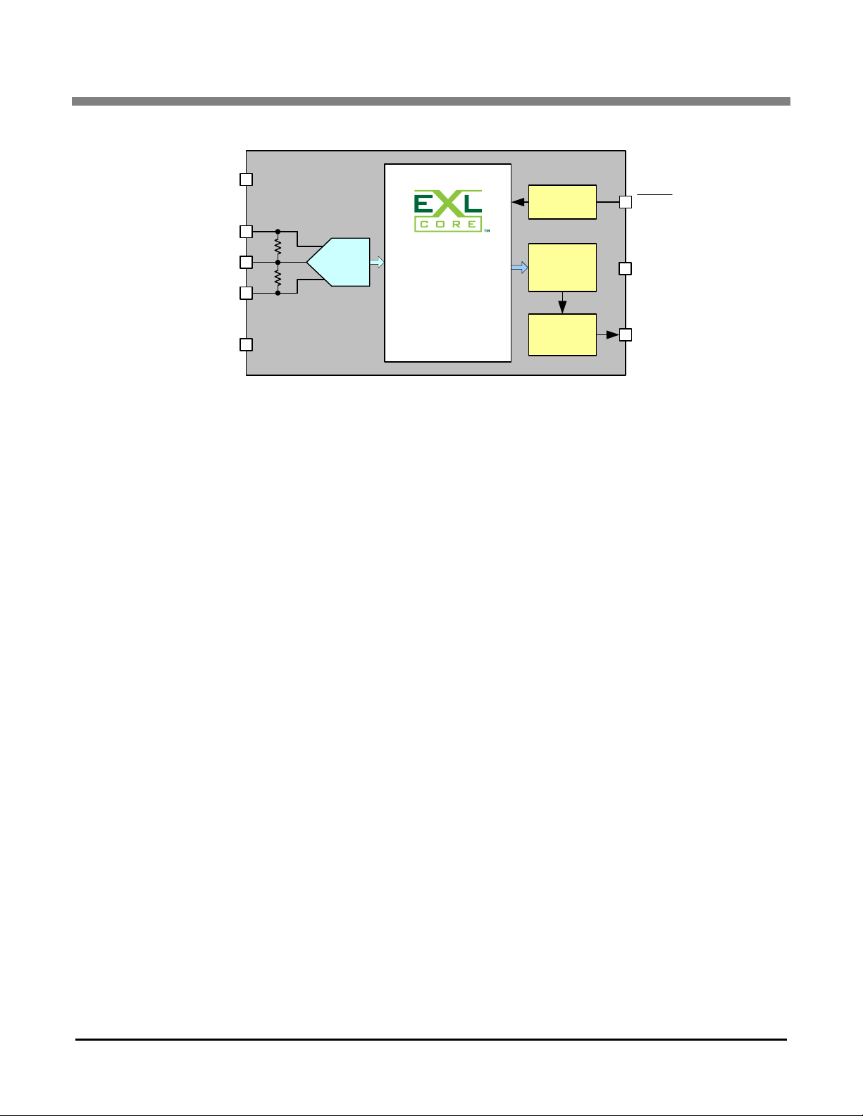
Figure 9. CS1500 Block Diagram
The CS1500 digital power factor controller operates in variable
on-time, variable frequency, discontinuous conduction mode
(DCM). The CS1500 uses a proprietary digital algorithm to
maximize the efficiency and reduce the conductive EMI.
The analog-to-digital converter (ADC) shown in the CS1500
block diagram in Figure 9 is used to sense the PFC output
voltage ( V
) and the rectified AC line voltage ( V
link
rect
) by
measuring currents through their respective resistors. The
magnitudes of these currents are measured as a proportion of a
reference current (I
) that functions as the reference for the
REF
ADCs. The digital signal is then processed in a control algorithm
which determines the behavior of the CS1500 during start-up,
normal operation, and under fault conditions, such as brownout,
overvoltage, overcurrent, overpower, and over-temperature
conditions.
• DCM with Variable On-Time, Variable Switching Frequency
The CS1500 PFC switching frequency varies with the
on a cycle-by-cycle basis, and its digital algorithm
V
rect
calculates the on-time accordingly for unity power factor.
Unlike traditional Critical Conduction Mode (CRM) PFC
controller, CS1500 operates at its low switching frequency near the zero-crossing point of the AC input voltage,
even no switching at all, and it operates at its high switching frequency at the peak of its AC input voltage (this is
the opposite of the switching frequency profile for a CRM
PFC controller), thus CS1500 reduces switching losses
especially under light-load conditions, spreads conducted
EMI energy peaks over a wide frequency band and increases overall system efficiency.
• Optimized Digital Loop Compensation
The proprietary digital control engine optimizes the feedback error signal using an adaptive control algorithm, im-
DS849A6 7
proves system stability and transient response. No
external feedback error signal compensation components
are required.
• Overcurrent Mitigation
The CS1500s digital controller algorithm limits the ON
time of the Power MOSFET by the following equation:
Where T
turned on and V
is the max time that the power MOSFET is
on
is the rectified line voltage. In the
rect
event of a sudden line surge or sporadic, high dv/dt line
voltages, this equation may not limit the ON time appropriately. For this type of line disturbance, additional protection mechanisms such as fusible resistors, fast-blow
fuses, or other current-limiting devices are recommended.
• Over Voltage Protection
Under steady-state conditions, the voltage loop keeps
PFC output voltage close to its nominal value. Under light
load startup or feedback loop open conditions, the output
voltage may pass the overvoltage protection threshold.
The digital control engine initiates a fast response loop to
shut down gate driving signal to reduce the energy delivered to the output for PFC capacitor protection. When the
link voltage drop below V
normal operation.
OVP-VOVP(Hy)
, PFC resumes
CS1500
Page 8

May ?$shortyear>
0
20
40
60
80
100
120
04590135180
Rectified Line Voltage Phase (Deg.)
% of Max
Switching Freq. (% of Max.)
Line Voltage (% of Max.)
% P
O max
F
SW max
(kHz)
Vin < 150 VAC
20
70
50
60
40
405
Burst Mode
20
0
60 80 100
Vin > 150 VAC
46
56
DCM Quasi CRM DCM Quasi CRM DCM
I
LB
t [ms]
I
AC
Inductor Current
t [ms]
V
link
[V]
100%
90%
Startup Mode
Normal
Mode
Startup Mode
Normal
Mode
CONFIDENTIAL
CS1500
3.1 PFC Operating Frequency
One key feature of the CS1500 is its operating frequency
profile. Figure 10 illustrates how the frequency varies over half
cycle of the line voltage in steady-state operation. When
power is first applied to the CS1500, it first examines the line
voltage and adapts its operating frequency to the exposed line
voltage as shown in Figure 11. The operating frequency is
varied in about a 2-to-1 ratio from the peak to the trough.
During start-up the control algorithm limits the maximum ontime, provides nearly square-wave envelop current within
every half line cycle by adjusting the operating frequency for
fast startup behavior.
Figure 10. Switching Frequency vs. Phase Angle
The CS1500 is designed to function as a DCM (discontinuous
conduction mode) controller, however it may operate in a
quasi-CRM operation mode near the peak periods. For
90~265VAC main input applications, PFC can be also
designed in quasi-CRM at a peak of 90VAC and full load as
shown in Figure 12.
Figure 12. DCM and quasi-CRM Operation with CS1500
3.2 Start-up vs. Normal Operation Mode
CS1500 has two discrete operation modes: Start-up and
Normal. Start-up mode will be activated when V
90% of nominal value and remains active until V
100% of nominal value, as shown in Figure 13. Startup mode
is activated during initial system power-up. Any V
less than 90% of nominal value, such as load change, can
cause the system to enter Start-up Mode until V
back into regulation.
is less than
link
reaches
link
drop to
link
is brought
link
Figure 11. Switching Frequency vs. Output Power
Figure 11 illustrates how the operating frequency (as a
percentage of maximum frequency) changes with output
power and the peak of the line voltage. Burst mode (when P
below 5%) will be discussed in a later section.
8 DS849A6
Figure 13. Start-up and Normal Modes
3.3 Burst Mode
Burst mode is utilized to improve system efficiency when the
system output power (P
implemented by intermittently disabling the PFC over a full
half-line period cycle under light load conditions, a s shown in
o
Figure 14.
) is < 5% of nominal. Burst mode is
o
Page 9

May ?$shortyear>
V
in
[V]
t [ms]
FET
V
gs
Burst Mode
Active
V
in
P
o
[W]
t [ms]
PFC
Disable
Burst Thres h o ld
P
o
αη
V
in min()
()×2×
V
link
V
in min()
2×()–
2f
maxLBVlink
×××
---------------------------------------------------------
×=
[Eq.1]
L
B
αη
V
in min()
()×
2
×
V
link
V
in min()
2×()–
2f
max
PoV
link
×××
---------------------------------------------------------
×=
[Eq.2]
R
FB
V
linkVdd
–
I
ref
--------------------------- -
=
[Eq.3]
R
FB
I
FB
VDD
ADC
V
link
7
FB
4
R
AC
I
AC
IAC
VDD
ADC
7
3
V
rect
R
AC
RFB=
[Eq.4]
CONFIDENTIAL
CS1500
Figure 14. Burst Modes
3.4 Output Power and PFC Boost Inductor
Maximum output power in normal mode is defined by the
following equation:
where, V
application requirements and maximum operating switching
frequency f
rated power (Po) against tolerances and transients. α is
typically set to 0.9.
The PFC Boost Inductor (LB in Figure 21) value can be
calculated using Equation 1 as follows:
, V
in(min)
max
, and LB are user defined based on
link
= 70kHz. α is a margin factor to guarantee
Resistor R
(shown as R2a & R2b in Figure 21) sets the
FB
feedback current and is calculated as follows:
Figure 15. Feedback Input Pin Model
The ADC is used to measure the magnitude of the I
current
FB
through resistor RFB. The magnitude of the IFB current is then
compared to an internal reference current, I
ref
.
By using digital loop compensation, the voltage feedback
signal does not require an external compensation network.
It is recommended that a ceramic capacitor of up to 2.2 nF be
placed between the FB pin and the VDD pin to filter noise in
the layout.
3.7 IAC Signal
where V
is volts RMS, V
in(min)
is volts DC, and α is set to
link
0.9.
3.5 PFC Output Capacitor
The value of the PFC output capacitor should be chosen
based upon voltage ripple and hold-up requirements. This is
described in more detail in the application section 4.1.6 PFC
Output Capacitor on page 13. To ensure system stability with
the digital controller, the recommended value of the capacitor
is within the range of 0.5 μF / watt to 2.0 μF/watt.
3.6 Output Feedback & Regulation
A current proportional to the PFC output voltage, V
supplied to the IC on pin FB and is used as a feedback control
signal. This current is compared against a fixed-value internal
reference current, I
DS849A6 9
.
ref
, is
link
A current proportional to the AC input voltage is supplied to the
IC on pin IAC and is used by the PFC control algorithm.
Resistor R
current and is calculated as follows:
For optimal performance, resistor RAC, RFB should use less
than 1% tolerance resistor. Resistors can be separated in two
Figure 16. IAC Input Pin Model
(shown as R1a & R1b in Figure 21) sets the IAC
AC
Page 10

May ?$shortyear>
116.8 ms=
[Eq.5]
T
Brownout
8ms
8ms
5V
------------
128V V
BP th()
–()56ms++=
8=
8
5
-- -
128 95–()56++
56 ms
56 ms
Start
Timer
Enter Standby Exit Standby
Upper
Lower
Brownout
Thresholds
Start Timer
T
Brownout
t [ms]
V
link
[V]
100%
90%
t
0
t0 + t
ovrpwr
Overpower
Startup Mode
Normal Mode
Startup Mode
Startup Mode
Normal Mode
Normal Mode
V
AC(rms )
90 265
P
o
P
o(max)
P
o
/ α
L = L
B
/ α
L = L
B
L < L
B
CONFIDENTIAL
CS1500
or more series elements if voltage breakdown or regulatory
compliance is of concern.
It is recommended that a ceramic capacitor of up to 2.2 nF be
placed between the IAC pin and the VDD pin to filter noise in
the layout.
3.8 Brownout Protection
Figure 17 illustrates the brownout protection mechanism
whereby the CS1500 enters standby, and upon recovery from
brownout, enters normal operation mode. In order to avoid the
fault trigger, a digital filter is added for line voltage detection.
The measured peak of the line voltage will be clamped to a
threshold (128 V) set by the IC within half of a line cycle if it is
higher than the threshold. It then decreases the voltage with a
slew rate of 5 V / trough (8 ms). The CS1500 initiates a timer
when the measured voltage falls below the lower brownout
threshold. The IC asserts the brownout protection and stops
the gate drive only if the timer reaches more than 56 ms,
which is set by the algorithm based on minimum line
frequency.
During the brownout state, the device continues monitoring
the input line voltage. The device exits the brownout state
when the input voltage peak value exceeds the brownout
upper threshold for at least 56 ms.
The maximum response time of the brownout protection
normally happens at light load conditions. It can be calculated
by the following equation:
protection is asserted, the IC stops gate drive, goes into a lowpower state, and restarts every 3 seconds. In the case of an
intermittent or minor fault, the device will continue to regulate the
output voltage (V
) to its nominal value.
link
If the PFC remains in startup mode for longer than a given
time, set by the digital controller, it senses an overload
condition and initiates the overpower protection.
The CS1500 has the ability to ensure nearly constant
overpower constraint over a wide range of line voltages, as
shown in Figure 19.
Figure 18. Overpower Protection Mechanism
In the brownout state, the PFC gate driver will restart every 3
seconds, trying to regulate V
to nominal value.
link
Figure 19. Maximal Output Power vs. Line Voltage
3.10 Overvoltage Protection
The overvoltage protection will trigger immediately and stop
the gate drive when the current into the FB pin (I
105% of the reference current value (I
gate drive switching when the link voltage drops below
Figure 17. Brownout Sequence
3.9 Overpower Protection
During normal operation, if the load is increased beyond the
overpower threshold, the output voltage starts falling. When the
output voltage is below the startup threshold voltage, the CS1500
switches to startup mode and the output voltage will rise back
again to the nominal value and will operate in normal mode if the
load is reduced to a normal level. Otherwise, the PFC oscillates
between startup mode and normal mode and the digital engine
declares the overpower condition. When the overpower
10 DS849A6
V
OVP–VOVP(HY)
3.11 Open/short Loop Protection
If the PFC output sense resistor RFB fails (open or short to
GND), the measured output voltage decreases at a slew rate
of about 2V / μs, which is determined by ADC sampling rate.
The IC stops the gate drive when the measured output voltage
is lower than the measured line voltage. The IC resumes gate
drive switching when the current into the FB pin becomes
larger than or equal to the current into the IAC pin and V
.
). The IC resumes
ref
) exceeds
OVP
link
is
Page 11
May ?$shortyear>
<1 nF
600 kΩ
See Te xt
VDD
STBY
GND
CS1500
CONFIDENTIAL
CS1500
greater than the peak of the line voltage (V
maximum response time of open/short loop protection for R
is about 150 μs in the CS1500.
If the PFC input sense resistor RAC fails (open or short to
GND), the current reference signal supplied to the IC on pin
IAC falls to zero. This failure is equivalent to a brownout
condition and will be handled by the brownout protection
mechanism described in Section 3.8.
rect(pk)
). The
FB
3.12 Overcurrent Limiting
Boost inductor saturation is a fatal condition for a PFC
converter. To prevent inductor current saturation conditions,
the IC utilizes a proprietary digital algorithm that keeps the
boost inductor current away from its saturation current. The
boost inductor should be designed for full load, minimal line
voltage, maximum switching frequency, and with enough
margin to prevent saturation in normal operation mode.
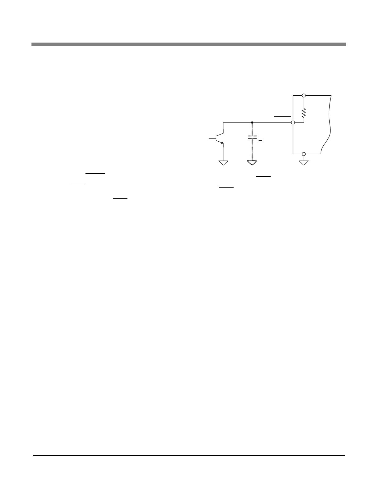
3.13 Standby (STBY) Function
The standby (STBY) pin provides a means by which an
external signal can cause the CS1500 to enter into a nonoperating, low-power state. The STBY
driven by an open-collector/open-drain device. Internal to the
pin, there is a pull-up resistor connected to the VDD pin as
input is intended to be
shown in Figure 20. Since the pull-up resistor has a high
impedance, the user may need to provide a filter capacitor (up
to 1000 p F) on this pin.
Figure 20. STBY Pin Connection
When the STBY
be tied to VDD (pulled high).
pin is not used, it is recommended that the pin
DS849A6 11
Page 12

May ?$shortyear>
D2
C1
D1
CS 1500
C2
L
B
C3
Q1
6
2
8
5
7
3
1
R1a
R1b
R2a
R2b
R3
FB
GD
NC
STBY
GND
VDD
IAC
NC
R
AC
R
FB
BR1
AC
Mains
Regulated
DC Output
4
Figure 21. CS1500 Basic Application Circuit
R
FB
V
linkVdd
–
I
ref
--------------------------- -
=
R
FB
400 12–
129 10
6–
×
--------------------------- -
=
R
FB
3.0MΩ=
[Eq.6]
R
AC
RFB=
R
AC
3.0MΩ=
[Eq.7]
PR
FB
()
V
link
2
R
FB
-------------- -
=
PR
FB
()
400
2
310
6
×
------------------
=
PR
FB
()53.3mW=
[Eq.8]
PRAC()max
265
2
310
6
×
------------------ -
=
PR
AC
()max
V
in max()
[]
2
R
AC
-----------------------------
=
PR
AC
()max 23.4mW=
[Eq.9]
4. APPLICATION EXAMPLE
CONFIDENTIAL
CS1500
The following sections describe an example application. The
example is based upon the typical connection diagram
illustrated in Figure 21.
4.1 PFC for Power Supply Application
The following design example is for a universal main inpu t,
front-end PFC converter with the following parameters:
V
in(min)
V
in(max)
V
P
link
o
90 VAC
265 VAC
400 V
90 W
Equations are provided to demonstrate how a user would
calculate the values for the components shown in the diagram.
Maximum power dissipation in each sense resistor is
calculated as follows (the equation ignores the voltage drop
& R
across R
IAC
IFB
):
4.1.1 IAC and IFB Sensing Inputs
The rectified AC input voltage (V
voltage (V
) are sensed as currents into the IC. The sensing
link
currents are set by resistors R
12 DS849A6
) and boosted PFC output
rect
and RFB, respectively:
AC
Page 13

May ?$shortyear>
C13.3
nF
W
------ -
P
o
×≥
C
1
3.3 120×≥
C
1
390nF≥ 0.39μF=
[Eq.10]
L
B
αη
V
in min()
()×2×
V
link
V
in min()
2×()–
2f
max
PoV
link
×××
---------------------------------------------------------
×=
LB0.9 0.95× 90
2
×
400 90 2×()–
27010
3
×()× 90× 400×
------------------------------------------------------------------ -
×=
LB374μ H=
[Eq.11]
I
LB pk()
4P
o
×
αη× V×
in min()
2×
----------------------------------------------------- -
=
I
LB pk()
3.3A=
I
LB pk()
490×
0.9 0.95× 90×
2
×
---------------------------------------------------- -
=
[Eq.12]
I
sat
0.001126
L
------------------------ -
≤
[Eq.13]
I
FET pk()ILB pk()
=
I
FET pk()
3.3A=
[Eq.14]
I
Dpk()ILB pk()
=
I
Dpk()
3.3A=
[Eq.15]
I
Davg()
P
o
V
link
----------- -
=
I
Davg()
0.225A=
I
Davg()
90
400
--------- -
=
[Eq.16]
[Eq.17]
C
out rip()
P
O
2π f
line min()
× V
link
×ΔV
link rip()
×
-------------------------------------------------------------------------------------- -
=
C
out rip()
90
2π 45× 400× 10×
------------------------------------------------ -
80μ Fu
useu100μF==
CONFIDENTIAL
4.1.2 PFC Input Filter Capacitor
To achieve unity power factor, a DCM PFC circuit needs an
input filtering circuit to bypass the high-frequency current so
that the input current consists of the low-frequency portion
only. There are two main factors on PFC input filter capacitor
selection: its voltage ripple and phase lag, which both will
worsen power factor. The filtering capacitance is proportional
and it is suggested as follows:
to P
o
Use 0.47 μF for tolerance.
If a PI filter used for suppression of conducted EMI is located
on the DC side of the input rectifier, the V
to be moved to the second capacitor.
4.1.3 PFC Boost Inductor
The value of the inductor in normal mode can be calculated by
the following equation, with α = 0.9 as a derating factor to
ensure the inductor is sized to guarantee DCM operation and
provide a slightly higher power than required by the load:
sense point has
rect
CS1500
4.1.4 PFC MOSFET
In normal mode, the PFC MOSFET peak current is equal to
the peak current in the PFC boost inductor:
4.1.5 PFC Diode
The PFC diode peak current in normal mode is the equal to the
inductor peak current:
The PFC Diode average current is calculated as follows:
Choose a 360 μH inductor.
η is the efficiency.
The inductor should be designed so that its saturation current
meets the following requirement, where 0.001126 is a predefined threshold for the current protection algorithm:
where L is the inductance in Henrys.
DS849A6 13
4.1.6 PFC Output Capacitor
The value of the output capacitor is determined by several
requirements. It must meet the voltage ripple and hold-up time
requirements and the RMS current in the capacitor should not
exceed its RMS current rating.
The following equation defines the size of the output capacitor
to meet the output voltage ripple requirements:
is the minimum line frequency the design is required
f
line(min)
to support, V
is the output voltage ripple requirement in volts peak-to-peak.
The equation will provide the value of the output capacitor
needed to meet the ripple requirement.
For 10 V of ripple and minimum line frequency of 45 Hz, the
equation becomes:
A second requirement that the output capacitor may be
required to meet is hold-up time. The value of the ca pacitor
is the output voltage from the PFC, ΔV
link
link(rip)
,
Page 14

May ?$shortyear>
C
out hold()
2P
O
× t×
hold
V
link
ΔV
out rip()
2
------------------------ -
–
2
V
link min()
()
2
–
------------------------------------------------------------------------------------------
=
[Eq.18]
C
out hold()
290× 0.010×
400
10
2
------
–
2
300()
2
–
------------------------------------------------------
27μ F==
V
ovp
V
link
1.05×=
V
ovp
400 1.05×=
V
ovp
420V=
[Eq.19]
CONFIDENTIAL
CS1500
needed to meet the hold-up time required is defined by the
following equation:
t
is the magnitude of the hold-up time in seconds. For
HOLD
10 ms of hold-up time and V
of 300 V, the equation
link(min)
becomes:
Choose a 100 μF capacitor.
4.1.7 Overvoltage Protection
Overvoltage protection is activated when V
of the nominal value:
While in overvoltage protection mode, gate drive output is
disabled. GD output is re-enabled when V
nominal value.
exceeds 105%
link
falls below its
link
14 DS849A6
Page 15

May ?$shortyear>
CONFIDENTIAL
4.1.8 Summary of Component Values
Designator Value Description
R1a 1.5 MΩ SFR25 axial film res - 0.4W-1%
R1b 1.5 MΩ SFR25 axial film res - 0.4W-1%
R2a 1.5 MΩ SFR25 axial film res - 0.4W-1%
R2b 1.5 MΩ SFR25 axial film res - 0.4W-1%
R3 4.7 Ω SFR25 axial film res - 0.4W-1%
C1 0.47 μF ECQ2W474KH
C2 0.47 μF 50V Ceramic cap - X7R
C3 100 μF, 450V LLS2W101MELA
BR1 4A, 600V GBU4J-BP
D1 1 A, 600 V 1N4005
D2 1 A, 600 V STTH1R06
LB 360 μH Premier Magnetics
CS1500
Q1 12 A, 500 V STP12NM50FP
CS1500 PFC Controller CS1500
DS849A6 15
Page 16
5. PERFORMANCE PLOTS
0
10
20
30
40
50
60
70
80
90
100
0102030405060708090100
Load (%)
THD(%)
Vin = 230
Vin = 115
Load (%)
Efficiency
70
75
80
85
90
95
100
0 102030405060708090100110
Vin=230V
Vin=115V
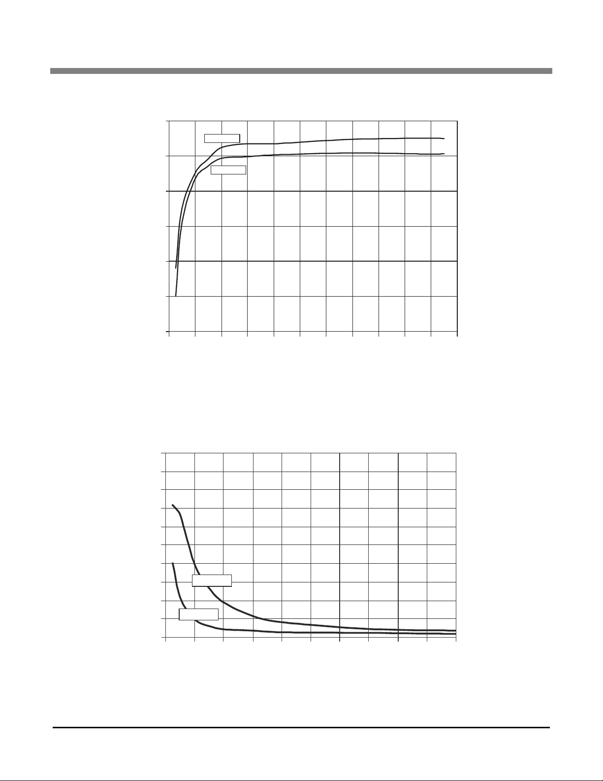
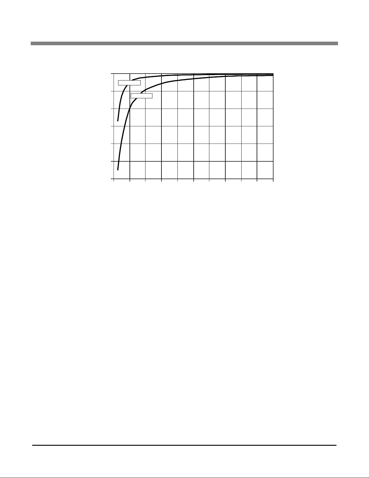
Figure 22. Efficiency vs. Load, Typi cal
Figure 23. Distortion vs. Load, Typical
May ?$shortyear>
CONFIDENTIAL
CS1500
16 DS849A6
Page 17
May ?$shortyear>
10
0.4
0.5
0.6
0.7
0.8
0.9
1
0 2030405060708090100
Load (%)
Power Factor
Vin = 115
Vin = 230
Figure 24. Power Factor vs. Load, Typica l
CONFIDENTIAL
CS1500
DS849A6 17
Page 18

May ?$shortyear>
Figure 25. Load Transient — 20% to 80% (60 mA to 240 mA), 0.8 A/μsec Slew, 90 VAC
Figure 26. Load Transient — 20% to 80% (60 mA to 240 mA), 0.8 A/μsec Slew, 260 VAC
CONFIDENTIAL
CS1500
18 DS849A6
Page 19

May ?$shortyear>
Figure 27. Overload — 240 mA to 500 mA, 90 VAC
Figure 28. Overload — 240 mA to 500 mA, 265 VAC
CONFIDENTIAL
CS1500
DS849A6 19
Page 20

May ?$shortyear>
CONFIDENTIAL
6. DEFINITIONS
Variable Definition
η The efficiency factor.
α A margin factor to guarantee rated power against tolerances and transient s.
f
line(min)
I
AC
I
FB
I
FET(pk)
I
rms
I
sat
I
st
I
ST
L
P
P
o(max)
R
AC
R
V
in(min)
V
link
V
link(min)
ΔV
link(rip)
V
rect
B
o
FB
The minimum AC line frequency.
The current generated by V
The current generated by V
The PFC MOSFET peak current, which is equal to the peak current in the PFC boost inductor.
that flows into the IAC pin.
rect
that flows into the FB pin.
link
The magnitude of the RMS current.
The boost inductor LB saturation current.
The sum of the current into the IAC and FB pins.
The startup current of the chip.
The PFC boost inductor .
The nominal output power from the CS1500 PFC circuit.
The maximum value of the output power from the CS1500 PFC circuit.
The sense resistor used to measure current into the IAC pin.
The sense resistor used to measure current into the FB pin.
The minimum specified line voltage for proper operation (volts RMS).
The magnitude of the output voltage from the PFC.
The magnitude of the output voltage from the PFC.
ΔV
, is the output voltage ripple requirement in volts peak-to-peak
link(rip)
The instantaneous value of the rectified line voltage (volts).
CS1500
20 DS849A6
Page 21

7. PACKAGE DRAWING
8L SOIC (150 MIL BODY) PACKAGE DRAWING
D
H
E
e
b
A1
A
c
L
∝
SEATING
PLANE
1
May ?$shortyear>
CONFIDENTIAL
CS1500
DIM MIN MAX MIN MAX
A 0.053 0.069 1.35 1.75
A1 0.004 0.010 0.10 0.25
B 0.013 0.020 0.33 0.51
C 0.007 0.010 0.19 0.25
D 0.189 0.197 4.80 5.00
E 0.150 0.157 3.80 4.00
e 0.040 0.060 1.02 1.52
H 0.228 0.244 5.80 6.20
L 0.016 0.050 0.40 1.27
∝
INCHES MILLIMETERS
0° 8° 0° 8°
JEDEC # MS-012
8. ORDERING INFORMATION
Part # Temperature Range Package Description
CS1500-FSZ -40 °C to +125 °C 8-lead SOIC, Lead (Pb) Free
9. ENVIRONMENTAL, MANUFACTURING, & HANDLING INFORMATION
Model Number Peak Reflow Temp MSL Rating
CS1500-FSZ 260 °C 2 365 Days
a. MSL (Moisture Sensitivity Level) as specified by IPC/JEDEC J-STD-020.
b. Stored at 30 °C, 60% relative humidity.
DS849A6 21
a
Max Floor Life
b
Page 22

Jun ?$shortyear>
Contacting Cirrus Logic Support
For all product questions and inquiries contact a Cirrus Logic Sales Representative.
To find one nearest you go to http://www.cirrus.com
IMPORTANT NOTICE
"Advance" product information describes products that are in development and subject to development changes.
Cirrus Logic, Inc. and its subsidiaries ("Cirrus") believe that the information contained in this document is accurate and reliable. However, the information is subject
to change without not ice and is provi ded "AS IS" wi thout warran ty of any kind (express or implied). Customers are advised to obtain the latest version of relevant
information to verify, before placing orders, that information being relied on is current and complete. All products are sold subject to the terms and conditions of sale
supplied at the time of order acknowle dgment, including tho se pertaining to warra nty, indemnification, and l imitation of liability. No responsibility is assumed by Cirrus
for the use of this information, including use of this inform ation as the b asis for ma nufacture or sale of any item s, or for infringement of patents or other rights of third
parties. This document is the property of Cirrus and by furnishing this information, Cirrus grants no license, express or implied under any patents, mask work rights,
copyrights, trademarks, trade secrets or other intellectual p roperty rights. Cirrus owns the copyr ights associated with the information con tained herein and gives consent for copies to be made of the information only for use within your organization with respect to Cirrus inte grated circu its or other products of Cirrus. This consent
does not extend to other copying such as copying for general distribution, advertising or promotional purposes, or for creating any work for resale.
CERTAIN APPLICATIONS USING SEMICONDUCTOR PRODUCTS MAY INVOLVE POTENT IAL RISKS OF DEATH, PERSONAL INJURY, OR SEVERE PROPERTY OR ENVIRONMENTAL DAMAGE ("CRITICAL APPLICATIONS"). CIRRUS PRODUCTS ARE NOT DESIGNED, AUTHORIZED OR WARRANTED FOR USE
IN PRODUCTS SURGICALLY IMPLANTED INTO THE BODY, AUTOMO TIVE SAFETY OR SECU RITY DEVICES, LIFE SUPPO RT PRODUCTS OR OTHE R CRITICAL APPLICATIONS. INCLUSION OF CIRRUS PRODUCTS IN SUCH APPLICATIONS IS UNDERSTOOD TO BE FULLY AT THE CUSTOMER'S RISK AND
CIRRUS DISCLAIMS AND MAKES NO WARRANTY, EXPRESS, STATUTORY OR IMPLIED, INCLUDING THE IMPLIED WARRANTIES OF MERCHANTABILITY
AND FITNESS FOR PARTICULAR PURPOSE, WITH REGARD TO ANY CIRRUS PRODUCT THAT IS USED IN SUCH A MANNER. IF THE CUSTOMER OR
CUSTOMER'S CUSTOMER USES OR PERMITS THE USE OF CIRRUS PRODUCTS IN CRITICAL APPLICATIONS, CUSTOMER AGREES, BY SUCH USE, TO
FULLY INDEMNIFY CIRRUS, ITS OFFICERS, DIRECTORS, EMPLOYEES, DISTRIBUTORS AND OTHER AGENTS FROM ANY AND ALL L IAB I LI TY, I NCLUDING ATTORNEYS' FEES AND COSTS, THAT MAY RESULT FROM OR ARISE IN CONNECTION WITH THESE USES.
Cirrus Logic, Cirrus, the Cirrus Logic logo designs, EXL CORE, and the EXL CORE logo designs are trademarks of Cirrus Logic, Inc. All other brand and product
names in this document may be trademarks or service marks of their respective owners.
CONFIDENTIAL
10.REVISION HISTORY
Revision Date Changes
A1 APR 2009 Initial Advance Information release.
A2 JUN 2009 No substantive changes. Document number incremented to avoid
confusion among previous, pre-released versions.
A3 DEC 2009 Revised feature list & product description. Revised electrical charac-
teristics to include brownout & open-loop protection. Modified defini-
tion table. Modified data sheet format.
A4 MAR 2010 Updated to correspond to C1 silicon.
A5 MAY 2010 Updated performance data.
A6 MAY 2010 Updated with additional test bench data for EP leve l.
CS1500
22 DS849A6
 Loading...