

Page 1
CRD5381
Audio A/D Converter w/ Asynchronous Decimation Filter
Reference Design
Features
Analog Performance
Advanced Multi-bit Delta-sigma Architecture
24-bit Conversion
120 dB Dynamic Range
-110 dB THD+N
Performance insensitivity to Input Clock Jitter
Digital Filter Characteristics
125 dB Stop-band Rejection
Phase-Matched Outputs
CS5381 A
LEFT
RIGHT
Quad Speed
Slave Mode
SDOUT
System Features
Output Sample Rate Determined by Input
Word, Left/Right, or Fsync Clock
No External Master Clock Required
Easily Scalable for Additional Channels
Sample Rates from 27 kHz to 192 kHz
Four-Channel Time-Division Multiplexed
Output
Two Independent Stereo, Left-Justified
Outputs
SDIN
CS8421 A
Master Input
Slave Ouput
SDOUT
Differential Analog
Inputs 1-4
http://www.cirrus.com
2
2
TDM ENABLE
SDOUT A
PCM Data Ouput/
Serial Clock Input
22
TDM IN
LEFT
RIGHT
CS5381 B
Quad Speed
Slave Mode
SDOUT
Copyright © Cirrus Logic, Inc. 2005
(All Rights Reserved)
CS8421 B
Master Input
Slave Output
SDOUTSDIN
TDM/SDOUT B
Header, J4
LRCK INPUT SCLK INPUT
MAY ‘05
DS563RD1
Page 2
CRD5381
Description
The combination of the CS5381 Analog-to-Digital Converter and CS8421 Asynchronous Sample Rate Converter
creates an analog-to-digital conversion system with an asynchronous digital decimation filter that is virtually
immune to interface or network jitter. In addition, the CS8421 adds a multi-channel Time Division Multiplexed
(TDM) output format option. These unique features address many of the issues and design challenge s associated
with networked audio systems and other high-performance applications. In addition to the standard 24-bit audio
data, the CS8421 adds the functionality to output properly dithered 32, 20, or 16-bit data.
The CRD5381 was designed as a platform for easy evaluation of the jitter rejection, sample rate conversion, and
time-division multiplexing capabilities of the CS8421 in the context of a A/D conversion system with an asynchronous decimation filter. The CRD5381 accepts four channels of balanced, analog audio input and provides four
channels of PCM data output. The data output can be either a four-channe l TDM format o r two indep end en t stereo
left-justified data outputs. The PCM data output is synchronous to the serial left-right clock and bit clock that the user
supplies. The CRD5381 also provides status indicators including ADC overflow and SRC unlock, and it accepts an
external reset signal. The only system power requirements for the design include +/- 12 Volts and +3.3 Volts. The
required input signals are a left/right or word clock and serial clock for the audio data output.
This document includes operational instructions and schematics for the CRD5381 and is a comp anion document to
the Cirrus Logic applications note AN270, “Audio A/D conversion with Asynchronous Decimation Filter” [1]. Please
also refer to the CS5381 and CS8421 data sheets for specific product information and specifications [2,3]. Both d ocuments, as well as AN270, are available online at http://www.cirrus.com
The CRD5381 schematic set is shown in Figures 9 through 14 and the board layout is shown in Figures 15
through 19. A block diagram of the CRD5381 is shown in Figure 8.
ORDERING INFORMATION
Product Description Order#
CRD5381 Audio A/D Converter w/ Asynchronous Decimation Filter Reference Design CRD5381
2 DS563RD1
Page 3

TABLE OF CONTENTS
1. SYSTEM OVERVIEW ................................................................................................................ 4
1.1 Sample Clock Domain ..................................... ... ....................................... ... .... ... ... ... ........ 4
1.1.1 CS8421 Input Operational Mode .......................................................................... 4
1.1.2 CS5381 Operational Mode . ... ... .... ... ... ... .... .......................................... ... ... ... ... ..... 4
1.1.3 Master Clock Frequency Generation .................................................................... 4
1.1.4 Maximum Sample Rate ................. ... ... ... ....................................... ... .... ... ... ... ... .... . 4
1.1.5 Synchronization of Multiple Sections .................................................................... 4
1.2 CS8421 Output and the Interface Clock Domain .............................................................. 5
1.2.1 CS8421 Output System Clocking .................................................... .... ... ... ... ... .... . 5
1.2.2 Serial Audio Output Port Options and Selection of Data Resolution and Dither ... 5
1.2.3 Clocking ........................................................... ... .... ... ...................................... .... . 5
1.2.4 SRC Locking and Varispeed ................................... ... ... ... ... .... ... ... ... .... ... ... ... ... .... . 5
1.2.5 Latency or Group Delay ............................................................. ... ... ..................... 6
1.2.6 Phase Matching Between Multiple Sections ......................................................... 6
1.3 Filter Response ................................................................................................................. 7
2. OPERATION .............................................................................................................................. 9
2.1 Sample Rate ............. .... ... ... ... ....................................... ... .... ... ... ........................................ 9
2.2 Audio Data Output Format Selection ......................... ........................................................ 9
2.3 System Clocking and Data I/O .......................................................................................... 9
2.4 System Status Indicators ................................................................................................. 10
2.5 System Reset ........ ... .... ...................................... .... ... ... ... .... ... ......................................... 10
2.6 Analog Inputs ......... ... .... ... ....................................... ... ... ... .... ... ......................................... 11
2.7 Power ........................................... ... ....................................... ... ... ... .... ... ......................... 11
2.8 Grounding and Power Supply Decoupling ....................................................................... 11
3. BLOCK DIAGRAM .................................................................................................................. 12
4. SCHEMATICS ......................................................................................................................... 13
5. LAYOUT .................................................................................................................................. 19
6. REFERENCES ......................................................................................................................... 24
7. REVISION HISTORY ............................................................................................................... 24
CRD5381
LIST OF FIGURES
Figure 1. Transitional Band, 48 kHz Out.........................................................................................7
Figure 2. Transitional Band, 96 kHz Out.........................................................................................8
Figure 3. Transitional Band, 192 kHz Out....................................................................................... 8
Figure 4. Left-Justified Serial Audio Interface.................................................................................9
Figure 5. TDM Audio Interface........................................................................................................ 9
Figure 6. Clock and Data Header Connections, J4....................................................................... 10
Figure 7. Status Indicator and Reset Header, J16........................................................................ 11
Figure 8. Block Diagram................................................................................................................ 12
Figure 9. Analog Inputs 1 & 2........................................................................................................ 13
Figure 10. Analog Inputs 3 & 4...................................................................................................... 14
Figure 11. CS5381 & CS8421 Pair A............................................................................................ 15
Figure 12. CS5381 & CS8421 Pair B............................................................................................ 16
Figure 13. I/O Header and Miscellaneous..................................................................................... 17
Figure 14. Power........................................................................................................................... 18
Figure 15. Silk Screen................................................................................................................... 19
Figure 16. Top Layer..................................................................................................................... 20
Figure 17. Bottom Layer................................................................................................................ 21
Figure 18. Power Plane................................................................................................................. 22
Figure 19. Ground Plane............................................................................................................... 23
DS563RD1 3
Page 4

1. SYSTEM OVERVIEW
1.1 Sample Clock Domain
1.1.1 CS8421 Input Operational Mode
Serial Audio Interface - Left-Justified. The selection of the serial audio interface format is arbitrary, assuming
the serial input format of the CS8421 is in agreement with the serial output format of the CS5381. The selection of the serial audio format is done by connecting a resistor (1.96 k Ω in this application) to either ground
or the VL supply.
System Clocking - Master mode, LRCK = MCLK/128. In this mode, the CS8421 generates the Serial and
Left/Right clocks within the sampling clock domain. This mode is selected by the resistor connected to the
MS_SEL pin of the CS8421. In this application the MS_SEL pin is connected to ground (equivalent to connecting a 1 kΩ resistor to ground).
1.1.2 CS5381 Operational Mode
Serial Audio Interface - Left-Justified. The selection of the serial audio interface format is arbitrary, assuming
the input format of the CS8421 is in agreement with the output format of the CS5381.
System Clocking - Slave mode. In this application the CS8421 generates the serial and Left/Right clocks
within the sampling clock domain.
CRD5381
Operational Mode or Sample Rate Range - Configured for Quad-Speed Mode to support sample rates
above 100 kHz.
High Pass Filter - Enabled
Master Clock Divide - Enabled to divide the master clock by 2.
1.1.3 Master Clock Frequency Generation
The CS8421 uses the clock supplied through its XTI pin as its master clock (MCLK). The CS5381 also uses
this signal as its master clock (through the MCLK pin). Alternatively, the CS8421 can generate a master
clock (via the MCLK_OUT pin) by connecting a crystal across its XTI-XTO pins, which can supply a MCLK
to the CS5381.
In this application, MCLK_OUT pin is not being used and is pulled high through a 47 kΩ resistor to VL to
disable it. If a crystal is not being used, as with the crystal oscillator in this application, XTO should be left
unconnected or pulled low through a 47 kΩ resistor to ground
1.1.4 Maximum Sample Rate
The maximum sample rate is limited by the maximum allowable master clock frequency of the CS8421,
which is 27 MHz. The sample rate is this clock frequency divided by 128. This corresponds to a maximum
sample rate of 210.937 kHz within the sample clock domain. In this application, we have chosen a master
clock frequency of 25 MHz, which corresponds to a sample rate of approximately 195.312 kHz
.
1.1.5 Synchronization of Multiple Sections
In this application multiple CS8421 inputs are set to master mode, and it is important that their serial ports
be aligned in time, with minimum possible phase error. To achieve this, their reset sign als are tied to gether
and routed for minimum skew. The amount of deviation between ILRCKs generated by the respective parts
is typically either 0 or 1 master clock period, or between 0 and 40 ns.
4 DS563RD1
Page 5

CRD5381
1.2 CS8421 Output and the Interface Clock Domain
1.2.1 CS8421 Output System Clocking
The CS8421 serial output is configured as a system clock slave. The advantages are:
• Output sample rate is dependent on the frequency o f the incoming word clock ( OLRCK), set by the user.
• Outputs of multiple CS8421 devices are synchronous.
• Multiple devices can be configured in a Time Division Multiplexed (TDM) multi-ch annel interface format.
As mentioned in “CS8421 Input Operational Mode” on page 4, the input of the CS8421 is configured as a
master, with the master clock frequency = 128*Fsi (or ILRCK). To accommodate this serial input mode, and
to set the serial output to slave, the MS_SEL pin is connected to +3.3 V.
1.2.2 Serial Audio Output Port Options and Selection of Data Resolution and Dither
The CS8421 provides multiple options for the serial audio output port. These options include:
• Output Data Format of Left-Justified, Right-Justified, I²S or TDM
• Audio output data resolution of the SRC can be set to 16, 20, 24, or 32-bits. Dithering is applied and is
automatically scaled to the selected output word length. This dither is not correlated between left and
right channels.
Output word-length and serial data format are selected with either a pull- up or pull down re sistor connected
to the SAOF pin of the CS8421. Please refer to Table 3 in the CS8421 data sheet for details [3].
The serial audio output of the CRD5381 is configured to operate in either dual 24-bit Left-Justified formats
or a 4-channel 24-bit TDM output.
1.2.3 Clocking
In order to ensure proper op eration of the CS8 421, the clo ck or crys tal attach ed to XTI m ust simult aneously
satisfy the requirements of LRCK for both the input and output as follows:
• If the input is set to master, Fsi ≤ XTI/128 and Fso ≤ XTI/130.
• If the output is set to master, Fso ≤ XTI/128 and Fsi ≤ XTI/130.
• If both input and output are set to slave, XTI ≥ 130*[maximum(Fsi,Fso)], XTI/Fsi < 3750, and XTI/Fso <
3750.
In the example application in this data sheet, the input serial port is set to master, and generates serial
clocks for a sampling rate of XTI/128. The output serial port is set as slave, and can receive a left-right clock
that is ≤ XTI/130. The serial bit-clock frequency is always 64*left-right clock.
1.2.4 SRC Locking and Varispeed
The SRC calculates the ratio between the input sample rate and the output sample rate, and uses this information to set up various parameters inside the SRC block. The SRC takes approximately 4200/Fso
(8.75 ms at Fso of 48 kHz) to make this calculation.
The SRC_UNLOCK pin is used to indicate when the SRC is not locked. When RST
is a change in Fsi or Fso, SRC_UNLOCK will be set high. The SRC_UNLOCK pin will continue to be high
until the SRC has reacquired lock and settled, at which point it will transition low. When the SRC_UNLOCK
pin is set low, SDOUT is outputting valid audio data. This can be used to signal a DAC to u n-mute its output.
DS563RD1 5
is asserted, or if there
Page 6
1.2.5 Latency or Group Delay
The system latency, or group delay, is the sum of the CS5381 group delay and the CS8421 group delay.
The latency of the CS5381 is 5 samples (5/Fs), and the latency o f the CS8421 depends on input and output
sample rates, and can be found in the CS8421 data sheet [3]. Table 1 shows the combined group delay for
typical output sample rates with a fixed input sampling rate of 195.3125 kHz.
.
Output Sample Rate Group Delay
48 kHz 1.48 ms
96 kHz .895 ms
192 kHz .605 ms
Table 1. System Latency
1.2.6 Phase Matching Between Multiple Sections
This phase delay is equal across multiple parts. Therefore, when multiple parts oper ate at the same Fsi and
Fso and use a common XTI/XTO clock, their output data is phase matched.
CRD5381
6 DS563RD1
Page 7
CRD5381
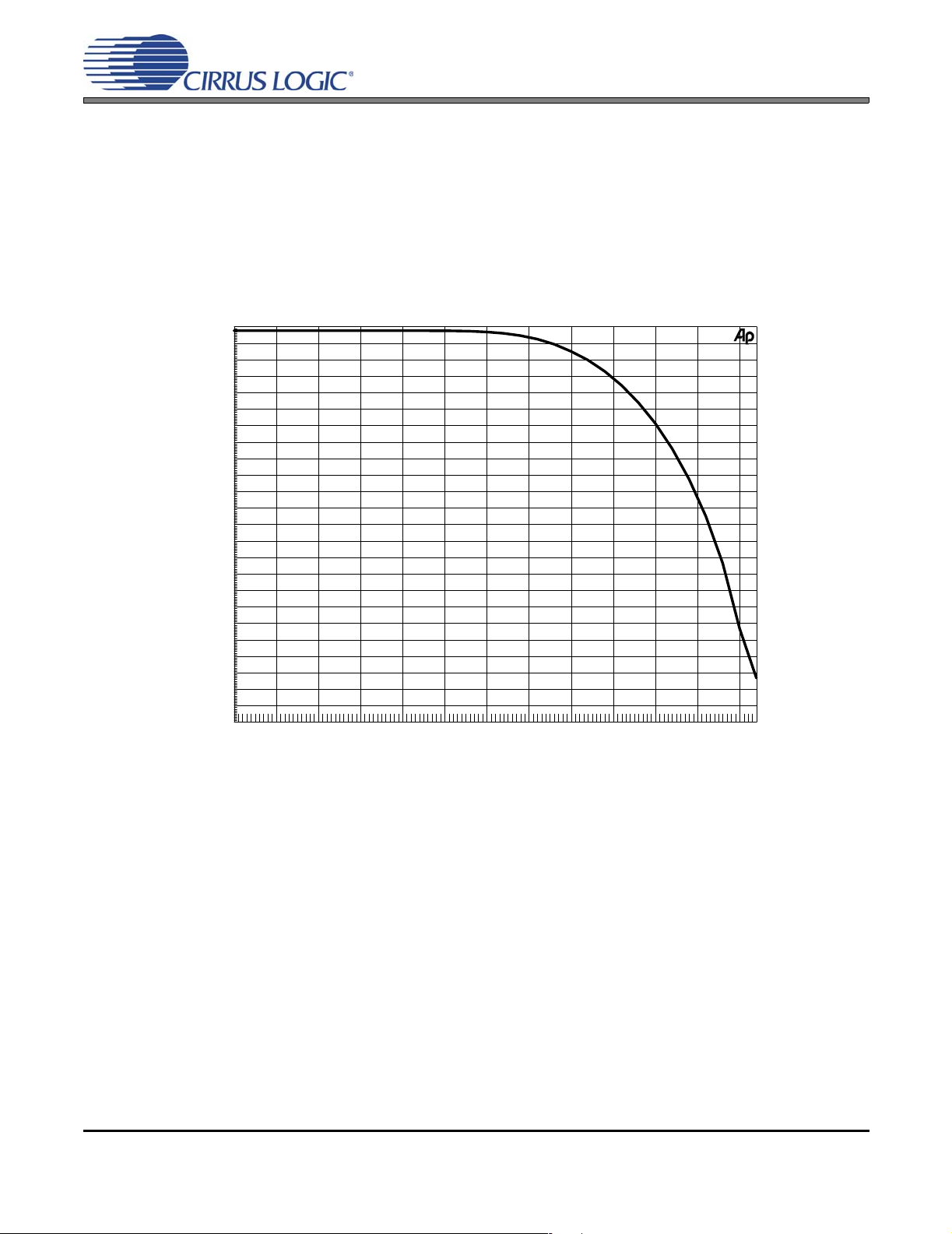
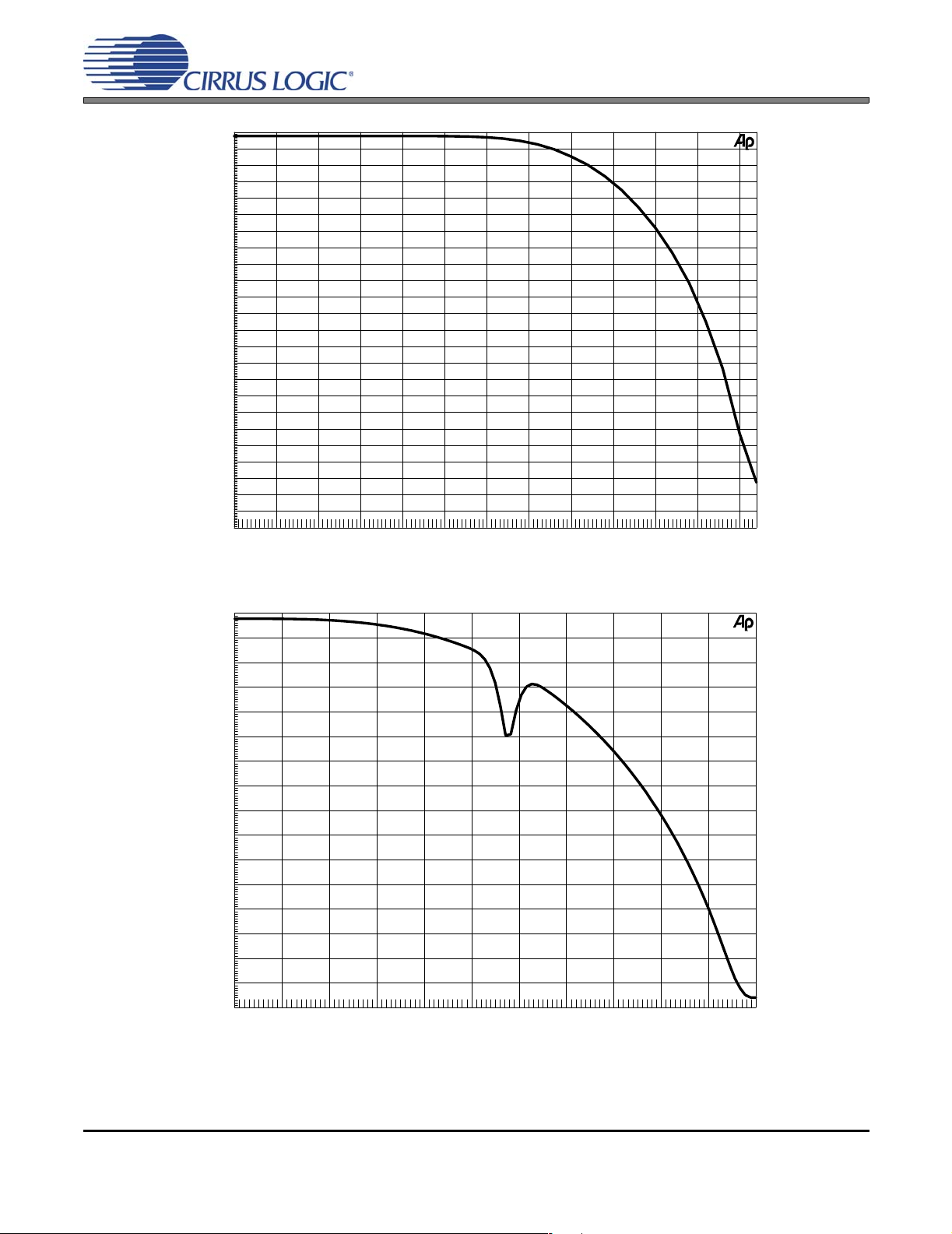
1.3 Filter Response
The transition-band response of the CRD5381 is due to the combination of the digital filtering performed by both th e
CS5381 and the CS8421. Due to the superior stop-band rejection of the CS8421, the combination of the two parts
yields a better stop-band rejection then the CS5381 alone. When the output sample rate is close to that of the
CS5381, signals that fall within the transition-band spectrum will already have been aliased down into the pass-band
prior to the CS8421’s output filter. This can be seen in Figure 3 on page 8, where the signals above the notch at
approximately 97.5 kHz represent signals that have been aliased downward prior to th e action of the CS8421 output
filter.
+0
-5
-10
-15
-20
-25
-30
-35
-40
-45
-50
-55
d
B
-60
F
S
-65
-70
-75
-80
-85
-90
-95
-100
-105
-110
-115
-120
20k 26k20.5k 21k 21.5k 22k 22.5k 23k 23.5k 24k 24.5k 25k 25.5k
Hz
Figure 1. Transitional Band, 48 kHz Out
DS563RD1 7
Page 8
+0
-5
-10
-15
-20
-25
-30
-35
-40
-45
-50
-55
d
B
-60
F
S
-65
-70
-75
-80
-85
-90
-95
-100
-105
-110
-115
-120
40k 52k41k 42k 43k 44k 45k 46k 47k 48k 49k 50k 51k
Hz
CRD5381
Figure 2. Transitional Band, 96 kHz Out
+0
-5
-10
-15
-20
-25
-30
-35
d
B
-40
F
S
-45
-50
-55
-60
-65
-70
-75
-80
40k 150k50k 60k 70k 80k 90k 100k 110k 120k 130k 140k
Hz
Figure 3. Transitional Band, 192 kHz Out
8 DS563RD1
Page 9

2. OPERATION
2.1 Sample Rate
Sampling Clock Domain - The Sampling clock domain includes the CS5381 A/D converter and the serial
audio input to the CS8421 SRC. The sampling frequency in this clock domain is dictated by the ILRCK frequency of each CS8421, and is derived from the system master clock Y2. The sample rate within this clock
domain is fixed at 195.312 kHz.
Interface Clock Domain - The Interface clock domain includes the output of the CS8421 SRC. The sample
rate of this domain is dictated by the frequency of the Le ft/Right or Word clock. This signal is an input to the
system and must be applied by the user through header J4.
2.2 Audio Data Output Format Selection
The CRD5381 allows selection of either a standard Left-Justified 3-wire serial audio interface with separate data lines for each ADC / SRC pair or a 4-channel TDM interface. Selectio n of either mode is accomplished via jumper J8. The two possible serial audio output formats are shown in Figures 4 and 5.
CRD5381
LRCK INPUT
SCLK INPUT
SDOUT
MSB MSBLSB LSB MSB
Channel A Channel B
Figure 4. Left-Justified Serial Audio Interface
LRCK
INPUT
SCLK
INPUT
TDM/
SDOUT B
MSB MSB MSB
SDOUT B (Left) SDOUT B (Right)
32 clks 32 clks 32 clks
Figure 5. TDM Audio Interface
2.3 System Clocking and Data I/O
Serial Clock - The Serial Clock must be applied by the user through header J4 in b oth L eft-J ustified an d
TDM mode. In TDM mode, Serial Clock must be 128*Left/Right Clock.
Left /Right or Word Clock - The Left/Right Clock must be app lied by the u ser th rough he ader J4 in both
Left-Justified and TDM mode. The output sample rate is determined by the frequency of this clock.
Serial Data Output - The serial data is output on J4. Separate stereo data outputs are available as
SDOUT A and TDM/SDOUT B when the Left-Justified form at is selected. Four-channel TDM data is available on TDM/SDOUT B (J4) when the TDM mode is selected.
SDOUT A (Left)
MSB
SDOUT A (Right)
32 clks
Figure 4 and Figure 5 illustrate Left-Justified and TDM data structures. Please refer to the “Slave Mode
Switching Specifications” on page 8 of the CS8421 data sheet for the timing require ments of both the LeftJustified and TDM modes[3].
Figure 6 illustrates the clock and data connections to J4.
DS563RD1 9
Page 10

CRD5381
Table 2 indicates the jumper options for J8 with the associated output data formats and some common
clock frequencies.
J8 SDOUT A Data Format
TDM/SDOUTB Data
Format
LRCK INPUT
Frequency
SCLK INPUT
Frequency
LJ 24-bit Left-Justified 24-bit Left-Justified 48 kHz 3.072 MHz
LJ 24-bit Left-Justified 24-bit Left-Justified 96 kHz 6.144 MHz
LJ 24-bit Left-Justified 24-bit Left-Justified 192 kHz 12.288 MHz
TDM - 4-Channel TDM 48 kHz 6.144 MHz
TDM - 4-Channel TDM 96 kHz 12.288 MHz
TDM - 4-Channel TDM 192 kHz 24.576 MHz
Table 2. Clock and Data Formatting Options
.
J4
Signal Ground
TDM/SDOUT B
LRCK INPUT
SCLK INPUT
SDOUT A
Figure 6. Clock and Data Header Connections, J4
2.4 System Status Indicators
ADC Overflow - Overflow indic ators are provided for each CS5381. Overflow is indicated by the LED la-
beled ADC OVERFLOW A (D4) or ADC OVERFLOW B (D5) being lit. These control signals are also av ailable as outputs on header J16, labeled OVERFLOW A
11.
SRC Unlock - SRC unlock indicators are provided for each CS8421. SRC unlock is indicated by the LED
labeled SRC UNLOCK A (D3) or SRC U NLOCK B (D2) being lit. These control signals are also available
as outputs on header J16, labeled SRC UNLOCK A and SRC UNLOCK B as shown in Figure 7 on page 11.
2.5 System Reset
The CRD5381 provides an on-board reset and a connection for a user-app lied reset signal thr ough head er
J16.
On-board Reset - The on-board reset signal is activated either upon power-up or by pressing push-button
S1. The reset signal is active-low, and is held low for approximately 350 ms after S1 has been pressed, or
power has been applied to the CRD5381.
External Reset - A connection is provided for a user to apply an external reset to the CRD5381 through
header J16 as shown in Figure 7 on page 11. The external reset should be an active-low, +3.3 V signal.
When an external reset signal is connected to the CRD5381, the on-board reset is the logical OR of the
power-up reset, the push-button reset, and the external reset.
and OVERFLOW B as shown in Figure 7 on page
10 DS563RD1
Page 11

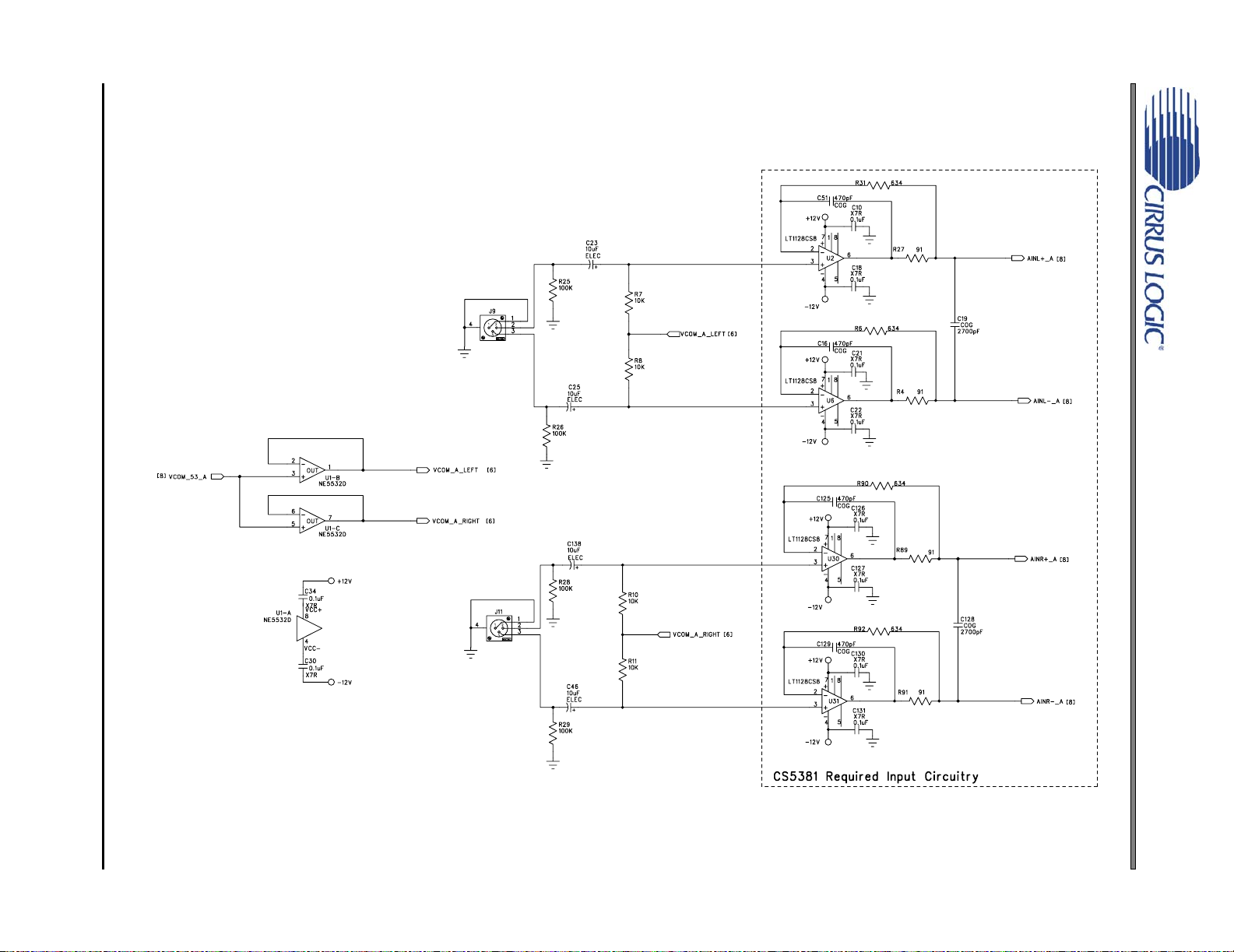
2.6 Analog Inputs
The CRD5381 provides four fully differential analog inputs via J9, J11, J7, and J12; shown in Figure 9 and
Figure 10. Each analog input has the required analog circuitry to optimize the per formance of each CS5381.
The input buffer to each CS5381 device has unity gain, and the CRD5381 differential input amplitude required to generate a full-scale digital output is typically 5.65 Vpp.
If extra analog input circuitry is required in the user’s design, it should drive a buffer equivalent to the contents of the dotted boxes shown in Figure 9 and in Figure 10 labeled “CS5381 Required Input Circuitry”. In
this case, all components outside the dotted boxes in Figure 9 and Figure 10 should be removed from the
design.
CRD5381
J16
Signal Ground
RESET
OVERFLOW A
OVERFLOW B
SRC UNLOCK A
SRC UNLOCK B
Figure 7. Status Indicator and Reset Header, J16
2.7 Power
The CRD5381 requires the user to supply +3.3 V (J6) and ±12 V (J2 and J1) to the board. Onboard regulators supply the required +5 V and +2.5 V. All voltage inputs must be referenced to the single black bananatype ground connector (J5). Zener Diodes Z1 and Z2 (shown in Figure 14) are used to protect the CRD5381
circuitry from accidental connection of a reversed polarity supply or a supply of over ± 13 V to J1 and J2.
WARNING:Please refer to the CS5381 and CS8421 data sheet for allowable voltage levels.
2.8 Grounding and Power Supply Decoupling
The CS5381 and CS8421 require careful attention to power supply and grounding arrangements in order
to optimize performance. Figure 8 provides an overview of the connections on the CRD5381; Figure 15
shows the component placement. Figure 16 shows the top layout, Figure 17 shows the bottom layout, Fig-
ure 18 shows the power plane, and Figure 19 shows the ground plane. The decoupling capacitors are lo-
cated as close to the CS5381 and CS8421 as possible. Extensive use of ground plane fill in the evaluation
board yields large reductions in radiated noise.
DS563RD1 11
Page 12

12 DS563RD1
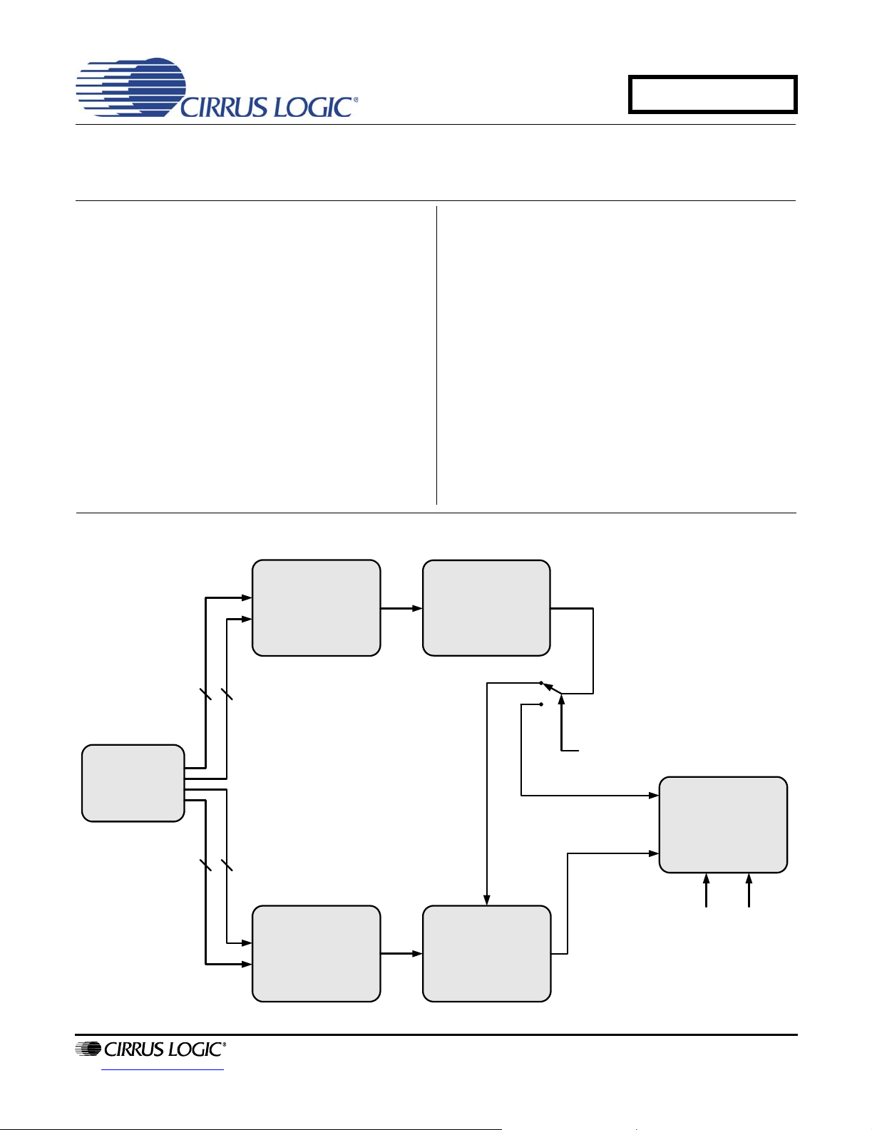
3. BLOCK DIAGRAM
Figure 9 on page 13 &
Figure 10 on page 14
Differential Analog
Inputs 1-4
Figure 11 on page 15
LEFT
CS5381 A
Quad Speed
RIGHT
Slave Mode
2
2
SCLK
LRCK
SDOUT
Figure 11 on page 15
ISCLK
ILRCK
SDIN
CS8421 A
Master Input
Slave Ouput
ENABLE
OSCLK
OLRCK
SDOUT
TDM
Figure 13 on page 17
INPUT SCLK
INPUT LRCK
PCM Data Ouput/
Serial Clock Input Header
SDOUT A
TDM/SDOUT B
22
LEFT
RIGHT
CS5381 B
Quad Speed
Slave Mode
Figure 12 on page 16
SCLK
LRCK
ISCLK
ILRCK
CS8421 B
Master Input
Slave Output
SDOUT
SDIN
Figure 12 on page 16
Figure 8. Block Diagram
TDM IN
OSCLK
OLRCK
SDOUT
CRD5381
Page 13
DS563RD1 13
4. SCHEMATICS
Figure 9. Analog Inputs 1 & 2
CRD5381
Page 14

14 DS563RD1
Figure 10. Analog Inputs 3 & 4
CRD5381
Page 15

DS563RD1 15
Figure 11. CS5381 & CS8421 Pair A
CRD5381
Page 16

16 DS563RD1
Figure 12. CS5381 & CS8421 Pair B
CRD5381
Page 17

DS563RD1 17
Figure 13. I/O Header and Miscellaneous
CRD5381
Page 18

18 DS563RD1
Figure 14. Power
CRD5381
Page 19

5. LAYOUT
CRD5381
Figure 15. Silk Screen
DS563RD1 19
Page 20

CRD5381
Figure 16. Top Layer
20 DS563RD1
Page 21

CRD5381
Figure 17. Bottom Layer
DS563RD1 21
Page 22

CRD5381
Figure 18. Power Plane
22 DS563RD1
Page 23

CRD5381
Figure 19. Ground Plane
DS563RD1 23
Page 24

6. REFERENCES
[1] AN270- Audio A/D Conversion w/ Asynchronous Decimation Filter web page:
http://www.cirrus.com
[2] CS5381 - 120 dB, 192 kHz Stereo A/D Converter web page:
http://www.cirrus.com/en/products/pro/detail/P1024.html
[3] CS8421 - 32-bit, 192 kHz, Asynchronous, Stereo Sa mple Rate Converter web page:
http://www.cirrus.com/en/products/pro/detail/P1082.html
7. REVISION HISTORY
Release Date Changes
DB1 MAY 2005 1st Release
Table 3. Revision History
CRD5381
Contacting Cirrus Logic Support
For all product questions and inquiries contact a Cirrus Logic Sales Representative.
To find the one nearest to you go to
IIMPORTANT NOTICE
Cirrus Logic, Inc. and its subsidiaries (“Cirrus”) believe that the information contained in this document is accurate and reliable. However, the information is subject
to change without noti ce and is pro vided “AS I S” without warranty of any kind (express o r impli ed). Cust omers are adv ised to ob tain the latest version of relevant
information to verify, before placing orde rs, that i nforma tion b ein g re lied on is curren t a nd com plete. All p roducts are so ld s ubject to the terms and conditions of sale
supplied at the time of order acknowledgment, including those pertaining to warranty, indemnification, and limitation of liability. No responsibility is assumed by Cirrus
for the use of this information, including use of this information as the basis for manufacture or sale of any items, or for infringement of patents or other rights of third
parties. This document is the property of Cirrus and by furnishing this information, Cirrus grants no license, express or implied under any patents, mask work rights,
copyrights, trademarks, trade secrets or other inte llectual property rights. Cirrus owns the copyrights associated with the information contained herein and gives consent for copies to be made of the information only for use within your organization with respect to Cirrus integrated circuits or other products of Cirrus. This consent
does not extend to other copying such as copying for general distribution, advertising or promotional purposes, or for creating any work for resale.
CERTAIN APPLICATIONS USING SEMICONDUCTOR PRODUCTS MAY INVOLVE POTENTIAL RISKS OF DEATH, PERSONAL INJURY, OR SEVERE PROPERTY OR ENVIRONMENTAL DAMAGE (“CRITICAL APPLICATIONS”). CIRRUS PRODUCTS ARE NOT DESIGNED, AUTHORIZED OR WARRANTED FOR USE
IN AIRCRAFT SYSTEMS, MILITARY APPLICATIONS, PRODUCTS SURGICALLY IMPLANTED INTO THE BODY, AUTOMOTIVE SAFETY OR SECURITY DEVICES, LIFE SUPPORT PRODUCTS OR OTHER CRITICAL APPLICATIONS. INCLUSION OF CIRRUS PRODUCTS IN SUCH APPLICATIONS IS UNDERSTOOD
TO BE FULLY AT THE CUSTOMER’S RISK AND CIRRUS DISCLAIMS AND MAKES NO WARRANTY, EXPRESS, STATUTORY OR IMPLIED, INCLUDING THE
IMPLIED WARRANTIES OF MERCHANTABILITY AND FITNESS FOR PARTICULAR PURPOSE, WITH REGARD TO ANY CIRRUS PRODUCT THAT IS USED
IN SUCH A MANNER. IF THE CUSTOMER OR CUSTOMER’S CUSTOMER USES OR PERMITS THE USE OF CIRRUS PRODUCTS IN CRITICAL APPLICATIONS, CUSTOMER AGREES, BY SUCH USE, TO FULLY I NDEMNIFY CIRRUS , ITS OFFI CERS, DIRECTORS, EMPLOYEES, DISTRIBUTORS AND OTHER
AGENTS FROM ANY AND ALL LIABILIT Y, INCLUDING ATTORNEYS’ FEES AND COSTS, THAT MAY RESULT FROM OR ARISE IN CONNECTION WITH
THESE USES.
Cirrus Logic, Cirrus, and the Cirrus Logic logo design s ar e tra de m a rks of Cir rus Lo gic, Inc. A ll oth er bra nd an d p ro du c t names in this document may be trademarks
or service marks of their respective owners.
www.cirrus.com
24 DS563RD1
 Loading...