

Page 1
CS48L10
32-Bit Audio DSP Product
CRD48L10-4in4out
Board Manual
http://www.cirrus.com
Copyright Cirrus Logic, Inc. 2012
(All Rights Reserved)
NOV 2012
DS998DB1
Page 2
Contacting Cirrus Logic Support
For all product questions and inquiries, contact a Cirrus Logic Sales Representative.
To find the one nearest you, go to www.cirrus.com.
IMPORTANT NOTICE
Cirrus Logic, Inc. and its subsidiaries (“Cirrus”) believe that the information contained in this document is accurate and reliable. However, the information is subject to change
without notice and is pr ov i de d “A S I S” wi t hou t war r an ty of a ny k i nd ( ex p res s o r impl i ed ). Cus to mer s ar e adv ise d to obtain the l at est ver sion of relev ant inf orma tion to veri fy,
before placing orders, that information being relied on is current and complete. All products a r e sold subject to the terms and conditions of sal e suppl i ed at t he ti me of or de r
acknowledgment, including those pertaining to warranty, indemnification, and limitation of liability. No responsibility is assumed by Cirrus for the use of th is information,
including use of this information as the b asis fo r manufacture or sale of any items, or for infringement of patents or other rights of third parties. This document is the property
of Cirrus and by furnishi ng thi s i nformation, Cirrus gran ts no license, express or implied under any patents, mask work rights, copyrights, trademarks, tr a de se cr et s or ot he r
intellectual proper ty rig hts. Cirr us owns t he co pyri ght s ass ociat ed with the i nf ormati on c onta ine d here in a nd giv es c onse nt f or copies to be made of the information only for
use within your organiz ation with respect to Cirrus integrated circuits or other products of Cirrus. This consent does not extend to other copying such as copying for general
distribution, advertising or promotional pu rp oses, or for creating any work for resale.
CERTAIN APPLICATIONS USING SEMICONDUCTOR PR ODUCTS MAY INVOLVE POTENTIAL RISKS OF DEATH, PERSONAL INJURY, OR SEVERE PROPERTY OR
ENVIRONMENTAL DAMAGE (“CRITICAL APPLICATI ONS”). CIRRUS PRODUCTS ARE NOT DESIGNED, AUTHORIZED OR WARRANTED FOR USE IN PRODUCTS
SURGICALLY IMPLANTED INTO THE BODY, AUTOMOTIVE SAFETY OR SECURITY DEVICES, LIFE SUPPORT PRODUCTS OR OTHER CRITICAL APPLICATIONS.
INCLUSION OF CIRRUS PRODUCTS IN SUCH APPLICATIONS IS UNDERSTOOD TO BE FULLY AT THE CUSTOMER’S RISK AND CIRRUS DISCLAIMS AND MAKES
NO WARRANTY, EXPRESS, STATUTORY OR IMPLIED, INCLUDING THE IMPLIED WARRANTIES OF MERCHANTABILITY AND FITNESS FOR PARTICULAR
PURPOSE, WITH REGARD TO ANY CIRRUS PRODUCT THAT IS USED IN SUCH A MANNER. IF THE CUSTOMER OR CUSTOMER’S CUSTOMER USES OR PER MITS
THE USE OF CIRRUS PRODUCTS IN CRITICAL APPLICATION S, CUSTOMER AGRE ES, BY SUCH USE, TO FULLY INDEMNIFY CIRRUS, ITS OFFICERS, DIRECTORS,
EMPLOYEES, DISTRIBUTORS AND OTHER AGENTS FROM ANY AND ALL LIABILITY, INCLUDING ATTORNEYS’ FEES AND COSTS, THAT MAY RESULT FROM OR
ARISE IN CONNECTION WITH THESE USES.
Cirrus Logic, Cirrus, and the Cirrus Logic logo designs are trademarks of Cirrus Logic, Inc. All other brand and product names in this document may be trademarks or service
marks of their respective owners.
I²C is a trademark of Philips Semiconductor.
Bluetooth is a registered trademark of the Bluetoo th Special Interest Group (SIG).
CS48L10
ii CRD48L10-4in4out Board Manual
Page 3

CS48L10
Chapter 1
Introduction to the CRD48L10-4in4out Board
1.1 Requirements ..................................................................................................................................................... 1-1
1.2 CRD48L10-4in4out Main Board Description ...................................................................................................... 1-1
1.3 Introduction to the CRD48L10 Kit ....................................................................................................................... 1-2
Chapter 2
Input/Output Specifications
2.1 Audio Inputs ........................................................................................................................................................2-1
2.1.1 Analog Line Input ......................................................................................................................................2-1
2.1.2 Analog Microphone Input .......................................................................................................................... 2-1
2.1.3 Optical Digital Input ................................................................................................................................... 2-1
2.1.4 Coaxial Digital Input ..................................................................................................................................2-1
2.1.5 Digital Microphone Inputs .......................................................................................................................... 2-1
2.1.6 I2S Digital Inputs ....................................................................................................................................... 2-1
2.2 Audio Outputs ..................................................................................................................................................... 2-2
2.2.1 Analog Line-level Outputs ......................................................................................................................... 2-2
2.2.2 Headphone Output .................................................................................................................................... 2-2
2.2.3 Ear Speaker Output ................................................................................................................................... 2-2
2.2.4 Speakerphone Left Output ........................................................................................................................2-2
2.2.5 Speakerphone Right Output ...................................................................................................................... 2-2
2.2.6 I2S Digital Output ...................................................................................................................................... 2-2
2.3 Digital Control Probe Points ............................................................................................................................... 2-3
2.3.1 DSP Control .............................................................................................................................................. 2-3
2.3.2 DSP Debug ............................................................................................................................................... 2-3
2.3.3 DSP Interrupts ........................................................................................................................................... 2-3
2.3.4 Codec Reset .............................................................................................................................................. 2-3
2.3.5 Codec I2C ................................................................................................................................................. 2-3
2.3.6 Codec Interrupt .......................................................................................................................................... 2-3
2.3.7 Main Clock ................................................................................................................................................. 2-4
2.4 DSP Composer Control Header ......................................................................................................................... 2-4
2.5 USB Power Input ................................................................................................................................................ 2-4
2.6 Input Button (S1) ............... ... ... ... .... ... ... .......................................... .................................................................... 2-4
2.7 MCU USER INTERFACE Header ............................................... .......................................... ... ... ....................... 2-4
2.8 Buttons and Knobs ............................................................................................................................................. 2-4
2.9 MCU DEBUG C-2 Programming Header ........................................................................................................... 2-5
2.10 Current Measurement Points ............................................................................................................................ 2-5
Chapter 3
Standalone Modes
3.1 S1 Button Control (No LCD) ............................................................................................................................... 3-1
3.1.1 Powering Up Board ...................................................................................................................................3-1
3.1.2 Selecting Input Audio Source ............................. ....................................................................................... 3-2
3.1.3 MP3 Decode from FLASH (U9) .................................................................................................................3-4
3.1.4 LINE IN ...................................................................................................................................................... 3-5
3.1.5 MIC 1 & 2 ..................................................................................................................................................3-6
3.1.6 S/PDIF ....................................................................................................................................................... 3-7
3.2 MCU UI Controlled ............................................................................................................................................. 3-7
3.2.1 Powering Up the Board ............................................................................................................................. 3-7
3.2.2 Project Menu ............................................................................................................................................. 3-8
3.2.3 Snapshot Menu ....................................................................................................................................... 3-11
3.2.4 AudioIn Source Menu ............................ ... ... ... .... ... ... ... .... ... ... ....................................... ........................... 3-11
3.2.5 Clock Source Menu ................................................................................................................................. 3-11
3.2.6 I2C Control Source Menu ........................................................................................................................ 3-12
Chapter 4
Quick Start for the CRD48L10-4in4out
4.1 Jumper Settings ..................................................................................................................................................4-1
CRD48L10-4in4out Board Manual 1
Page 4

4.2 Powering Board .................................................................................................................................................. 4-1
4.3 Monitoring Audio ................................................................................................................................................. 4-2
4.4 Selecting Audio Input Source ............................................................................................................................. 4-2
4.5 USB Control of CRD48L10-4in4out ......................... .............................................. ............................................. 4-2
CS48L10
Chapter 5
Using DSP Composer™ with CRD48L10-4in4out
Chapter 6
Updating the MCU Image
6.1 Checking the Revision of MCU Code in the Board ............................................................................................. 6-1
6.2 Checking the Revision of MCU Code Included in the SDK ............................................ .... ... ... ... ... .... ... .............6-1
6.3 Programming the MCU ....................................................................................................................................... 6-1
Chapter 7
Using Micro-Condenser to Create and Load a FLASH Image
7.1 Generate Deliverables ........................................................................................................................................ 7-1
7.2 Creating the Flash Image, and Programming the CRD48L10 ............................................................................ 7-1
Chapter 8
Programming MP3 FLASH
Chapter 9
Master Boot Usage
9.1 SPI Master Boot ................................................................................................................................................. 9-1
9.2 I2C Master Boot ..................................................................................................................................................9-2
Chapter 10
External Control of CRD48L10-4in4out
10.1 External Control of CS48L10 .......................................................................................................................... 10-1
10.2 External Control of CRD48L10-4in4out Board ............................................................................................... 10-1
Chapter 11
Measuring Power
Chapter 12
Using Analog MEMS Microphones
Chapter 13
Interfacing to Telit GSM Module
Chapter 14
Schematic, Layout, BOM
Chapter 15
Revision History
2 CRD48L10-4in4out Board Manual
Page 5
Chapter 1
Introduction to the CRD48L10-4in4out Board
Table 1-1. CRD48L10 Kit Contents
Item Quantity
Cirrus Logic CRD48L10 Board 1
Cirrus Logic CRD48L10 MCU USER INTERFACE Bo ard 1
Cirrus Logic CDB-MCU-DEBUG Board 1
USB cable A-Mini 2
Stereo audio cables RCA female, 3.5 mm male 1
5x2 ribbon cable 1
7x2 ribbon cable 1
15x2 ribbon cable 1
TOSLINK female to TOSLINK mini male adapter 2
Doc card universal DSP 1
Doc evaluation board disclaimer notice 1
1.1 Requirements
1.1 Requirements
This section lists the requirements for the CRD48L10-4in4out evaluation board:
• PC requirements
•Microsoft
• USB 2.0 support
• Software requirements
• Cirrus DSP Software Development Kit (available from your local Cirrus Logic representative)
• Support hardware requirements
• Digital or analog audio source (for example, DVD player, PC with a digital audio card/device)
• Speakers for audio playback (for example, powered PC speakers, AVR/amp + speakers, stereo speakers) or
headphones
• Cabling requirements
• Digital audio inputs—TOSLINK optical or coaxial cable with 1/8” plug (connect to digital audio card or DVD
player); audio stream input/output (ASIO) card.
• Digital audio output—TOSLINK optical cable
• Analog Audio Inputs—1/8” stereo plug microphone or line in cable (connect microphone or line in to ADC)
• Analog Audio Outputs—1/8” stereo plug for lineout and headphones, speaker/speakerphone outputs use 2x1
headers.
®
Windows XP™ or Windows 7™ operating system.
1.2 CRD48L10-4in4out Main Board Description
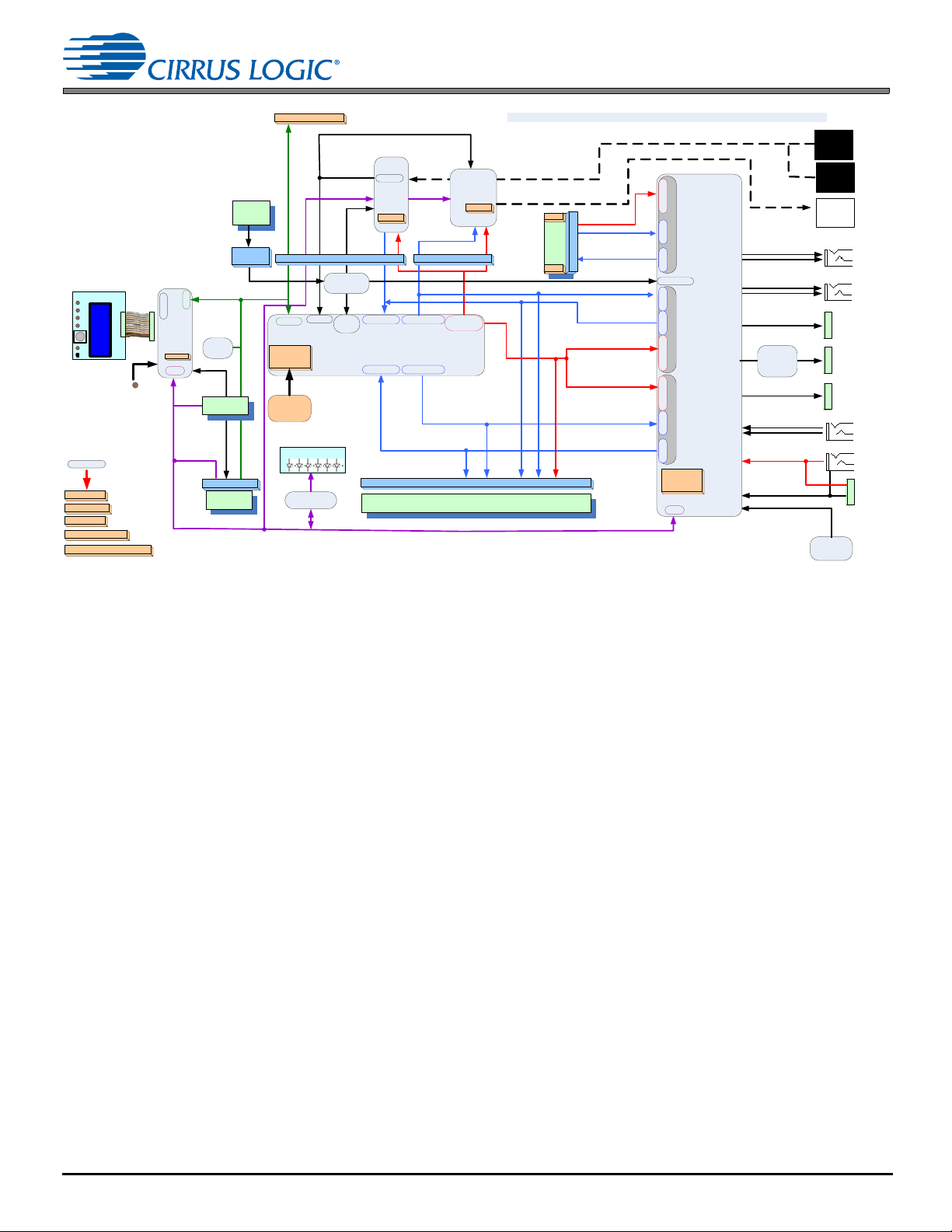
Fig. 1-1 shows a detailed block diagram of the CRD48L10-4in4out board.
1
Page 6
SiLab
MCU
SPI
I2C
HP
EAR
SPKR-L
+1v8
DSP
FLASH
SCP Probe H DR
(SPI, I2C )
+5V -> +4v0
+3v3 -> +1v 8
+3v3 -> +1v0 / +1v2
Control & MP3
USB
Digital MIC
Header
Line
Out
HEADER
MIC1
MIC2
CS42L73
CODEC
ASP
SDI
CHAS
CS48L10
DSP
I2S DAI2
I2C
I2S
Clocks
SCP
+1v0 / +1v2
+1v8
+1v8
+5v0
Current
Sense
Header
JP2 CTRL HDR
I2S DAO2
MCLK
REF
CLK
Line In
SDO
XSP
CLOCKS
SDI
I2S DAI1 I2S DAO1
CS8416
CS8406
RMCK
+3v3
+3v3
Mini -
OPTICAL
RX
Mini-
OPTICAL
TX
CRD48L10 – 4IN4OUT
Level Transl at ion
HEADER
SPKR-R
CS35L01
VSP
CLOCKS
SDI SDO
GSM Tellit HDR
+3v3 -> +1v8 (Translator VL)
I2S Probe HDR (DAI[2:1], DAO[2:1], Clocks)
Level Translation
+5V -> +3v3 (SPDIF)
12.288 MHz
OSC
MCLK1
Level Transl at ion
CLOCKS
SDO
Level Translation
Dongle Active
+4v0 -> +3.3V
+4v0
+3v0
Level Translation
c
USB +5V
c
INPUT MODE
SELECT
LCD
LCD Button board
JP6
JP1
INPUT SOURCE DISPLAY
I/O Expander
HEADE R
uHDMI
Level
Translation
CLK HDR
Coax
RX
1.3 Introduction to the CRD48L10 Kit
The main components to be familiar with on the board are:
The main purpose of this board is to allow a customer to evalua te the Cirru s Lo gic CS4 8L 10 DSP a nd othe r Cir rus Log ic
analog semiconductors in a complete audio subsystem.
The Silicon Labs MCU handles the SPI, I²C, and GPIO to control the board components. USB control of the DSP is
possible by connecting the CDB-MCU-DEBUG dongle to the JP2 header.
1.3 Introduction to the CRD48L10 Kit
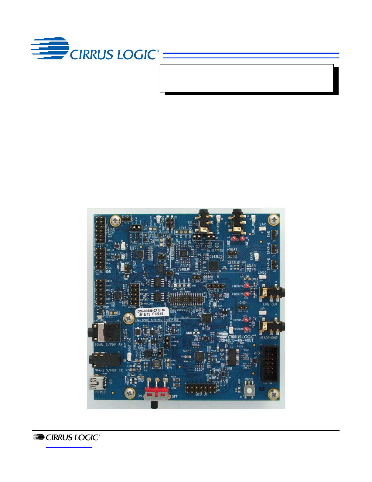
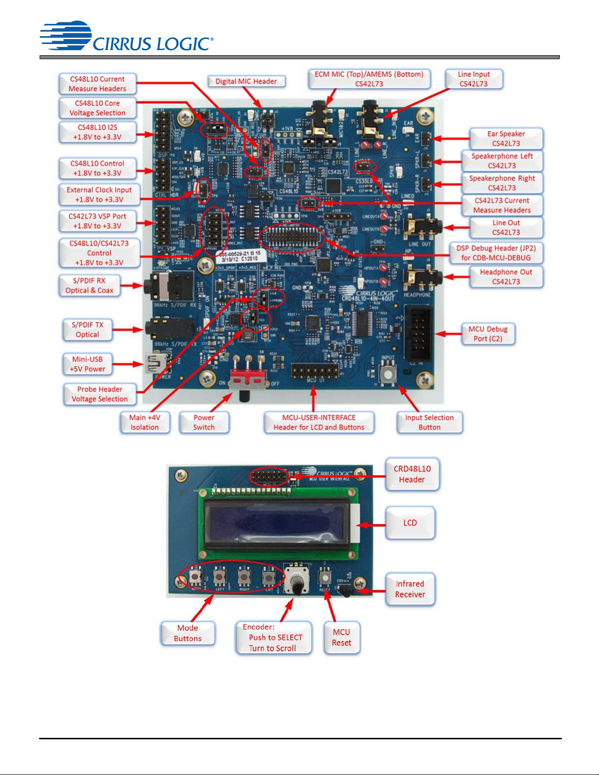
Fig. 1-2 shows a picture of the CRD48L10-4in4out with labels on the important connections. Fig. 1-3 shows a picture of
the CRD48L10 MCU-USER-INTERFACE board. Fig. 1-4 shows a picture of the CDB-MCU-DEBUG board. Fig. 1-5 shows
a picture of the supplied ribbon cables. Fig. 1-6 shows a pictur e of the supplied mini-USB and 1/8 ” to RCA cables. Fig.1-7
shows a picture of the TOSLINK to mini TOSLINK adapter.
2
Figure 1-1. CRD48L10-4in4out Bloc k Diagram
• CS48L10 DSP
• CS42L73 Ultra Low-power CODEC
• CS35L01 Mono Class-D Amplifier
• CS8416 S/PDIF Rx
• CS8406 S/PDIF Tx
™
C8051F930 MCU
• Silicon Labs
Page 7
1.3 Introduction to the CRD48L10 Kit
Figure 1-2. CRD48L10-4in4out
Figure 1-3. MCU-USER-INTERFACE Board
3
Page 8
1.3 Introduction to the CRD48L10 Kit
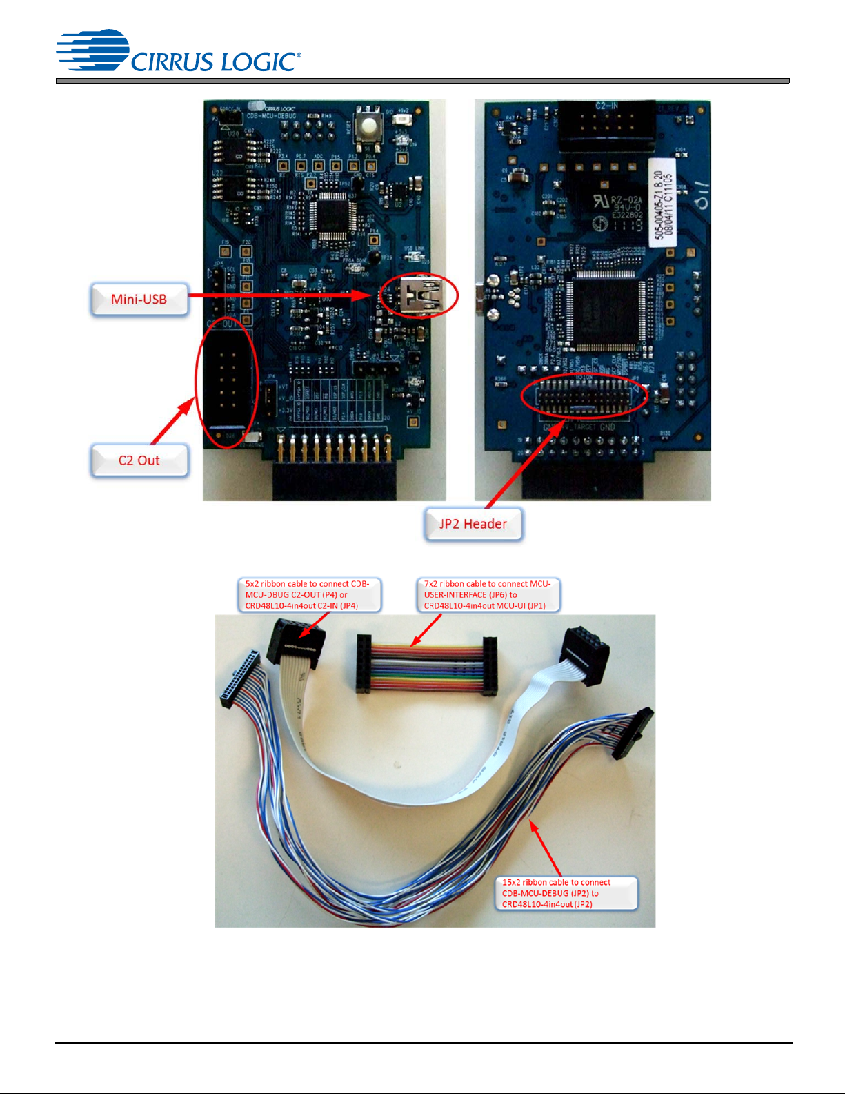
Figure 1-4. CDB-MCU-DEBUG Board
Figure 1-5. Ribbon Cables
4
Page 9
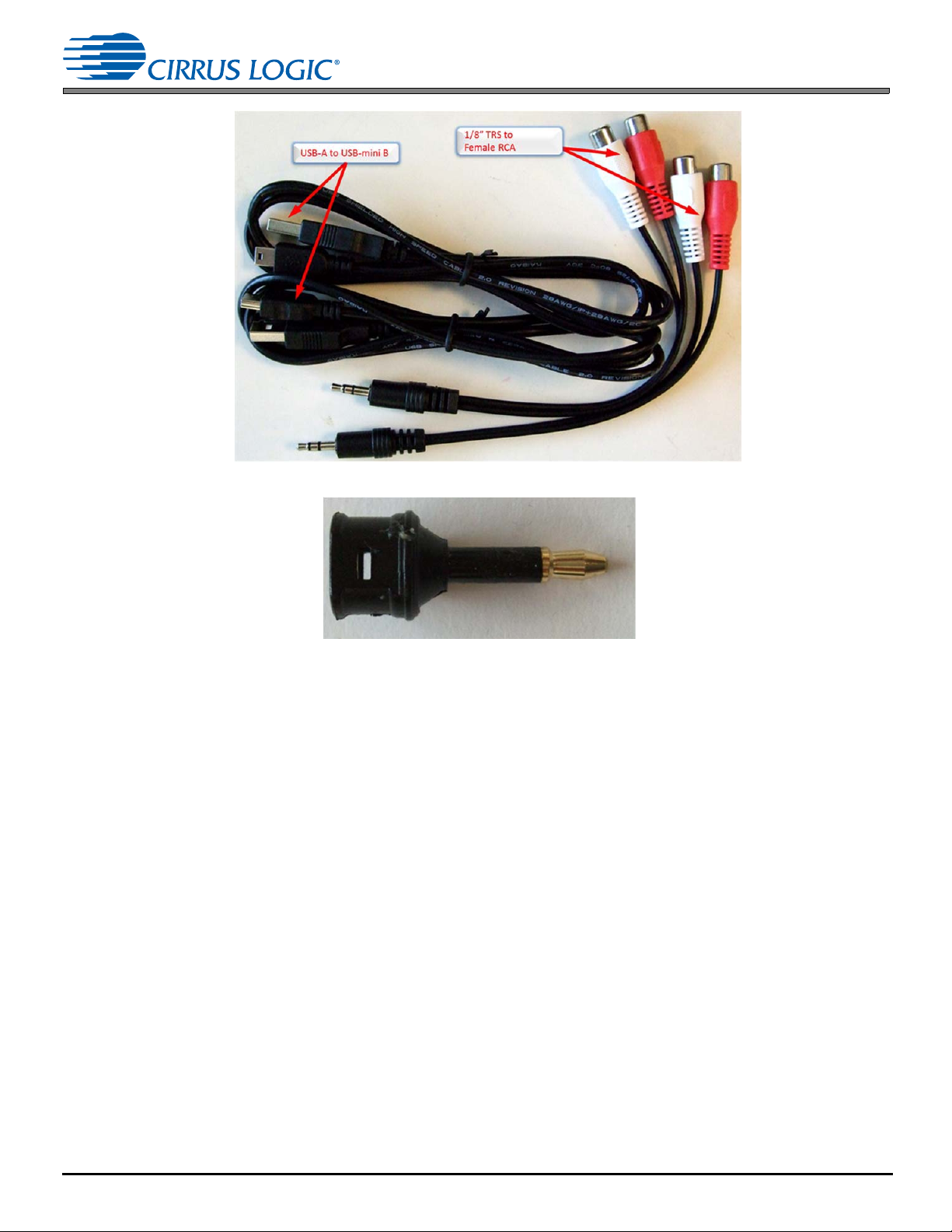
Figure 1-6. USB and 1/8” to RCA Cables
1.3 Introduction to the CRD48L10 Kit
Figure 1-7 . TO SLINK to Mini Male Adapter
5
Page 10

Chapter 2
Input/Output Specifications
2.1 Audio Inputs
2.1.1 Analog Line Input
• Connector Type: 1/8 inch (3.5mm) stereo Female
• Absolute Maximum Signal Level: +2.1 V
• Absolute Minimum Signal Level: –0.3 V
• Full Scale Amplitude (PGA VOL = 0 dB): 1.44 Vpp
• Reference Designators: J2 (LINE IN)
2.1.2 Analog Microphone Input
• Connector Type: 1/8 inch (3.5mm) stereo Female
• Absolute Maximum Signal Level: +2.1 V
• Absolute Minimum Signal Level: –0.3 V
• Full Scale Amplitude (PGA VOL = 0 dB/MIC PREAMP = +10 dB): 464 mVpp
• Full Scale Amplitude (PGA VOL = 0 dB/MIC PREAMP = +20 dB): 144 mVpp
• Reference Designators: J1 (MIC 1 & 2)
2.1 Audio Inputs
2.1.3 Optical Digital Input
• Connector Type: Fiber Optic Mini TOSLINK RX for Digital Audio
• Reference Designators: J4 (OPTICAL)
2.1.4 Coaxial Digital Input
• Connector Type: 1/8 inch (3.5mm) stereo Female
• Absolute Maximum Signal Level: +3.6 V
• Absolute Minimum Signal Level: –0.3 V
• Reference Designators: J4 (COAXIAL)
2.1.5 Digital Microphone Inputs
• Connector Type: 0.1 inch Male Header
• Absolute Maximum Signal Level: +2.1 V
• Absolute Minimum Signal Level: –0.3 V
• Reference Designators: J13 (DMIC)
2.1.6 I2S Digital Inputs
• Connector Type: 0.1 inch Male Header
• Absolute Maximum Signal Level: +6.5 V
• Absolute Minimum Signal Level: –0.5 V
• Reference Designators: TP3 (DSP), TP14 (VSP)
1
Page 11

2.2 Audio Outputs
2.2.1 Analog Line-level Outputs
• Connector Type: 1/8 inch (3.5mm) stereo Female
• Full Scale Output: 2.9 Vpp
• Reference Designators: J3 (LINE OUT)
2.2.2 Headphone Output
• Connector Type: 1/8 inch (3.5mm) stereo Female
• Full Scale Output: 1.5 Vpp
• Power: 2 x 17 mW (at THD+N = –60 dB)
• Minimum Load: 16 ohms
• Reference Designator: J5 (HEADPHONE)
Note: This output has the same data as J3 (LINE OUT).
2.2.3 Ear Speaker Output
• Connector Type: 100-MIL Male Header (2x1)
• Full Scale Differential Output: 2.3 Vpp (Digital Volume = –2.5 dB)
• Power: 0.51 W (at THD+N = –60 dB)
• Minimum Load: 16 ohms
• Reference Designator: J10 (EAR)
2.2 Audio Outputs
2.2.4 Speakerphone Left Output
• Connector Type: 100-MIL Male Header (2x1)
• Full Scale Differential Output: 5.8 Vpp (Digital Volume = –5.5 dB)
• Power: 0.53 W (at THD+N = –62 dB)
• Minimum Load: 8 ohms
• Reference Designator: J11 (SPKR-L)
2.2.5 Speakerphone Right Output
• Connector Type: 100-MIL Male Header (2x1)
• Full Scale Differential Output: 7.2 Vpp (Digital Volume = –3.5 dB)
• Power: 1.0 W (at THD+N = –74 dB)
• Minimum Load: 4 ohms
• Reference Designator: J12 (SPKR-R)
2.2.6 I2S Digital Output
• Connector Type: 100-MIL Male Header (6x2)
• Maximum Signal Level: +V_PROBE
• Reference Designators: TP3 (DSP), TP14 (VSP)
2
Page 12

2.3 Digital Control Probe Points
2.3.1 DSP Control
• Connector Type: 100-MIL Male Header (5x2)
• Absolute Maximum Input Signal Leve l: + 6. 5 V
• Absolute Minimum Input Signal Level: –0.5 V
• Maximum Signal Output Level: +V_PROBE
• Reference Designators: JP3 (CTRL HDR), TP15
2.3.2 DSP Debug
• Connector Type: 100-MIL Male Header (4x1)
• Absolute Maximum Input Signal Leve l: + 2. 0 V
• Absolute Minimum Input Signal Level: –0.5 V
• Maximum Signal Output Level: +1.8 V
• Reference Designators: TP10
2.3.3 DSP Interrupts
• Connector Type: 100-MIL Male Header (4x1)
• Absolute Maximum Input Signal Leve l: + 2. 0 V
• Absolute Minimum Input Signal Level: –0.5 V
• Maximum Signal Output Level: +1.8 V
• Reference Designators: TP1
2.3 Digital Control Probe Points
2.3.4 Codec Reset
• Connector Type: 100-MIL Male Header (5x2)
• Absolute Maximum Input Signal Leve l: + 6. 5 V
• Absolute Minimum Input Signal Level: –0.5 V
• Maximum Signal Output Level: +V_PROBE
• Reference Designators: TP15
2.3.5 Codec I2C
• Connector Type: 100-MIL Male Header (4x1)
• Absolute Maximum Input Signal Leve l: + 2. 0 V
• Absolute Minimum Input Signal Level: –0.5 V
• Maximum Signal Output Level: +1.8 V
• Reference Designators: TP11
2.3.6 Codec Interrupt
• Connector Type: 100-MIL Male Header (5x2)
• Absolute Maximum Input Signal Leve l: + 2. 0 V
• Absolute Minimum Input Signal Level: –0.5 V
• Maximum Signal Output Level: +1.8 V
• Reference Designators: TP15
3
Page 13

2.3.7 Main Clock
• Connector Type: 100-MIL Male Header (2x1)
• Absolute Maximum Input Signal Leve l: + 6. 0 V
• Absolute Minimum Input Signal Level: –0.5 V
• Reference Designators: TP4 (CLKIN)
2.4 DSP Composer Control Header
• Connector Type: 50-MIL Male Header (15x2)
• Absolute Maximum Input Signal Leve l: + 2. 0 V
• Absolute Minimum Input Signal Level: –0.5 V
• Maximum Signal Output Level: +1.8 V
• Reference Designators: JP2
2.5 USB Power Input
The USB power input has the following characteristics and is switched by S8:
• Voltage Range: +4.75 VDC to +5.25 VDC
• Minimum Power: +5 V supply (0.5 A)
• Connector Type: USB Mini-B
• Reference Designator: USB1
2.4 DSP Composer Control Header
2.6 Input Button (S1)
The button S1 (located near JP4) is used to change the audio input source.
2.7 MCU USER INTERFACE Header
• Connector Type: 100-MIL Male Header (7x2)
• Absolute Maximum Input Signal Leve l: + 3. 6 V
• Absolute Minimum Input Signal Level: –0.5 V
• Maximum Signal Output Level: +1.8 V
• Reference Designators: JP1
2.8 Buttons and Knobs
The buttons S9–S14 (located on MCU-USER-INTERFACE board) are used to control the MCU.
• S9 (Rotary Encoder)—Turn this knob to navigate u p/down thr oug h men u page . Press do wn o n the kno b to sele ct
an item
• S10 (Menu)—This button displays the CRD48L10 board configuration options.
• S11 (Left)—This button takes you back one level in the menu system.
• S12 (Right)—This button takes you one level deeper in the men u system.
• S13 (Exit)—This button exits the CRD48L10 board configuration menu.
• S14 (Reset)—This button executes a hard reset of the on-board MCU.
4
Page 14

2.9 MCU DEBUG C-2 Programming Header
2.9 MCU DEBUG C-2 Programming Header
This header is used to program the MCU from a CDB-MCU-DEBUG dongle (P4/C2-OUT connector) OR the Silicon Labs
programming dongle.
• Connector Type: Shrouded 100-MIL Male Header (5x2)
• Absolute Maximum Input Signal Leve l: + 3. 6 V
• Absolute Minimum Input Signal Level: –0.5 V
• Maximum Signal Output Level: +1.8 V
• Reference Designators: JP4
2.10 Current Measurement Points
• Connector Type: 100-MIL Male Header (1x2)
• Reference Designators: TP20–TP23, P16
5
Page 15

Dig ital MIC
MIC1
MIC2
Line In (L)
Line In (R)
ASP OUT
XSP OUT
DAI1
DAI2
Level
Translation
DAO1
DAO2
Level
Translation
SPDIF TX
(CS8406 )
ASP IN
XSP IN
Speakerphone (L)
Speakerphone (R)
AMP
(CS3501 )
EAR
Headphone Outputs (L&R)
Line Outputs (L& R)
(CS42L73 )
Min i Opt i c al RX
Mini Optical TX
VSP OUTVSP IN
Level Translation
GS M Telit HDR
MCU
(C8051 F930)
1MB SPI FLASH
(SST25WF080)
1MB SPI FLASH
(SST25WF080)
JP2 H DRI2C
SPI
SCP
6 r esi s tor ladder
buttons
5 gr een LE D s
1 SPDIF ON LED
(CS48 L10)
(For DSP Master Boot )
(For DSP Slave Boot )
Level
Translation
I2C to 8-bit
I/O Expander
(PCF8574 )
8 blue LEDs for audio
I/O active indications
TP11(JP3 H DR)
ADC
DAC
DAC
SPDIF RX
(CS8416 )
3.1 S1 Button Control (No LCD)
Chapter 3
Standalone Modes
The CRD48L10-4in4out has multiple audio input and output ports. All available data flo w paths are shown in the diagr am
in Fig. 3-1.
Figure 3-1. Data Flow Paths
The data path can be selected using either the mode select button S1 on the CRD48L10-4in 4out or with the
MCU-USER-INTERFACE board. The data path opt ion s ava ila ble usin g on ly S 1 are a sub se t of th os e ava ila ble with th e
MCU-USER-INTERFACE board. The two modes will be described in separate sections below.
It is worth noting that the VSP port of the CS42L73 is always available for external audio through TP14, but not with the
default MCU code provided with the CRD48L10-4in4out. An external MCU must configure the CS42L73 to utilize audio
data from the VSP.
3.1 S1 Button Control (No LCD)
3.1.1 Powering Up Board
When powering on the CRD48L10 board, the power LEDs D5–D9 should illuminate indicating that all power rails are good
and the output connector LEDs D4, D8, D10, D11, and D20 should illuminate to show that the MCU has configured the
codec to drive audio out of the board. No input mode LEDs are illuminated since default input mode is from on-board
FLASH. Power up state of the CRD48L10 is shown in Fig. 3-2.
1
Page 16

3.1 S1 Button Control (No LCD)
Figure 3-2. CRD48L10-4in4out S1 Control Only
3.1.2 Selecting Input Audio Source
Input selection is controlled with the S1 button, as shown in Fig 3-3, on the CRD48L10 board. By default, the Input will
DSP play back an MP3 from on-board FLASH U9. There is an LED next to each input to indicate which input is active,
except when in FLASH playback where no input LED will be illuminated.
Figure 3-3. S1 Input Selection Button
2
Page 17

3.1 S1 Button Control (No LCD)
The MCU will cycle through the inputs when the button S1 is pressed from FLASH > LINE IN > MIC 1 & 2 > S/PDIF >
FLASH. LED locations are shown in Fig. 3-4 to Fig. 3-6.
If the MCU-USER-INTERFACE board is attached, the LCD also displays the active input.
Figure 3-4. LINE IN Active
Figure 3-5. MIC 1 & 2 Active
3
Page 18

Digital MIC
MIC1
MIC2
Line In (L)
Line In (R)
ASP OUT
XSP OUT
DAI1
DAI2
DAO1
DAO2
ASP IN
XSP IN
Speakerphone (L)
Speakerphone (R)
AMP
(CS3501 )
EAR
Headphone Outputs (L&R)
Line Outputs (L&R)
(CS42 L73)
VSP OUTVSP IN
SCP
(CS48 L10)
ADC
DAC
DAC
FLASH
U9
MCU
C8051
3.1 S1 Button Control (No LCD)
Figure 3-6. S/PDIF OPTICAL Active
Each of the input modes is described in the following sections.
The MCU configures the data paths shown feeding the DSP in the following data path dia grams. Inactive paths are shown
in gray. The DSP project determines how the audio is processed and which audio goes out each DAO port. The default
DSP projects programmed into the CRD48L10 are configured to process the audio paths shown in blue.
3.1.3 MP3 Decode from FLASH (U9)
Figure 3-7. Data Path for FLASH Playback
4
Page 19

(CS48L 10)
(CS42L73 )
CLOCK
MCLK1
MCLK
SCLK LRCLK
SCLK ( ASP/XSP )
LRC LK (ASP/XSP)
OSCILLATOR
12.288 M Hz
Digital MIC
MIC1
MIC2
Line In (L)
Line In (R)
ASP OUT
XSP OUT
DAI1
DAI2
DAO1
DAO2
ASP IN
XSP IN
Speakerphone (L)
Speakerphone (R)
AMP
(CS3501 )
EAR
Headphone Outputs (L&R)
Line Outputs (L&R)
(CS42 L73)
VSP OUTVSP IN
SCP
(CS48L10 )
ADC
DAC
DAC
Level
Translation
(CS48L10)
(CS42L73)
SPDIF RX
(CS8416 )
CLOCK
MCLK1
MCLK
SCLK LRCLK
SCLK (ASP/XSP)
LRC LK ( ASP /XSP)
SCLK
LRCLK
OSCILLATOR
12 .288 M H z
Mini Optical RX
Or
1/8" Coax
3.1 S1 Button Control (No LCD)
Figure 3 -8. Clocking for FLASH Playback–DSP Master
This is the default configuration after power up of the CRD48L10-4in4out. Power up and connect headphones to the
HEADPHONE jack or a speaker to the LINE OUT jack, and you will hear audio playing in a continuous loop.
3.1.4 LINE IN
Figure 3-9. Data Path for LINE IN Audio
Figure 3-10. Clocking for LINE IN Audio–DSP MCLK Slave
5
Page 20

Digital MIC
MIC1
MIC2
Line In (L)
Line In (R)
ASP OUT
XSP OUT
DAI1
DAI2
DAO1
DAO2
ASP IN
XSP IN
Speakerphone (L)
Speakerphone (R)
AMP
(CS3501 )
EAR
Headphone Outputs (L&R)
Line Outputs (L&R)
(CS42 L73)
VSP OUTVSP IN
SCP
(CS48L10 )
ADC
DAC
DAC
Level
Translation
(CS48L10)
(CS42L73)
SPDIF RX
(CS8416 )
CLOCK
MCLK1
MCLK
SCLK LRCLK
SCLK (ASP/XSP)
LRC LK ( ASP /XSP)
SCLK
LRCLK
OSCILLATOR
12 .288 M H z
Mini Optical RX
Or
1/8" Coax
3.1 S1 Button Control (No LCD)
The S/PDIF receiver is configured to automatically switch between the on-board oscillator and the clock recovered from
an incoming S/PDIF stream.
In the previous diagram, any time a valid S/PDIF stream is presented to the CS8416, the system audio clock will be locked
to the Fs of the incoming stream. The S/PDIF cable should be removed when the on-board oscillator (or TP4) is meant to
master audio clocks.
3.1.5 MIC 1 & 2
Figure 3-11. Data Path for MIC 1 & 2 Audio
The S/PDIF receiver is configured to automatically switch between the on-board oscillator and the clock recovered from
an incoming S/PDIF stream.
In the previous diagram, any time a valid S/PDIF stream is presented to the CS8416, the system audio clock will be locked
to the Fs of the incoming stream. The S/PDIF cable should be removed when the on-board oscillator (or TP4) is meant to
master audio clocks.
6
Figure 3-12. Clocking fo r MIC 1 & 2 Audio–DSP MCLK Slave
Page 21

3.1.6 S/PDIF
Digital MIC
MIC1
MIC2
Line In (L)
Line In (R)
ASP OUT
XSP OUT
DAI1
DAI2
SPDIF RX
(CS8416)
Level
Translation
DAO1
DAO2
Level
Translation
SPDIF TX
(CS8406 )
ASP IN
XSP IN
Speakerphone (L)
Speakerphone (R)
AMP
(CS3501 )
EAR
Headphone Outputs (L&R)
Line Outputs (L&R)
(CS42L73)
Mini Optical RX
Or
1/8" Coax
Mini Optical TX
VSP OUTVSP IN
SCP
(CS48L10)
ADC
DAC
DAC
Level
Translation
(CS48L10)
(CS42L73)
SPDIF RX
(CS8416 )
CLOCK
MCLK1
MCLK
SCLK LRCLK
SCLK (ASP/XSP)
LRC LK ( ASP /XSP)
SCLK
LRCLK
OSCILLATOR
12 .288 M H z
Mini Optical RX
Or
1/8" Coax
3.2 MCU UI Controlled
Figure 3-13. Data Path for S/PDIF Audio
Both the Mini-Optical and 1/8” Coax inputs are connected to the S/PDIF Receiver, but only on e can be active at any time
(there is only one physical plug). If both the optical and coax were active, the S/PDIF Receiver would be unable to recover
clock or data.
3.2 MCU UI Controlled
3.2.1 Powering Up the Board
When powering on the CRD48L10 board, the power LEDs D5-D9 should illuminate indicating that all power rails are good
and the output connector LEDs D4, D8, D10, D11, and D20 should illuminate to show that the MCU has configured the
codec to drive audio out of the board. No input mode LEDs are illuminated since default input mode is from on-board
FLASH. Power up state of the CRD48L10 is shown in Fig. 3-15.
Figure 3-14. Clocking for S/PDIF Audio–DSP MCLK Slave
7
Page 22

3.2 MCU UI Controlled
Figure 3-15. CRD48L10-4in4out MCU UI Control
1. The LCD will then display the current revision of the on board C8051F930 MCU, as shown below:
2. The MCU will attempt to read a micro_condenser image from the SPI FLASH. If it fails you will get the following
error:
3. The MCU will cycle through displays showing the status of the Audio Source, Project:, and Snapshot:
4. Using the buttons and rotary encoder knob on the MCU User Interface board it is possible to configure the
CRD48L10 in more ways than is possible just using button S1.
5. Push the “Menu” button to bring up the con figur ation me nu on th e LCD. Turn the encoder knob to choose different
sub-menus, and press the encoder knob down to select an option.
3.2.2 Project Menu
A project is a collection of firmware modules and configurations downloaded to the DSP to process audio in a specific way.
For the CRD48L10-4in4out, the Project also defines how the board is configured and data is routed to/from the CS48L1 0.
The Project menu selection on the LCD appears as shown in Fig. 3-16.
Figure 3-16. Project Menu
8
Page 23

3.2 MCU UI Controlled
There are four projects available in the default MCU code shipped with the CRD48L10:
• MP3 Decode from FLASH
• LINE IN
• MIC IN
•S/PDIF IN
Each project is described in the following sections.
3.2.2.1 MP3 Decode from FLASH (U9) Project
This project is selected, as shown in Fig. 3-17.
Figure 3-17. MP3 Decode from FLASH
This project is the same as described in Section 3.1.3. There is only one snapshot available for this project.
3.2.2.2 LINE IN Project
This project is selected, as shown in Fig. 3-18.
Figure 3-18. LINE IN Project
This project is the same as described in Section 3.1.4. There is only one snapshot available for this project.
3.2.2.3 MIC 1 & 2 Project
This project is selected, as shown in Fig. 3-19.
Figure 3-19. MIC IN Project
This project is the same as described in Section 3.1.5. There is only one snapshot available for this project.
3.2.2.4 S/PDIF Project
This project is selected, as shown in Fig. 3-20.
Figure 3-20. S/PDIF IN Project
The S/PDIF project available through the MCU User Interface is more flexible than that described in Section 3.1.6. This
project allows the mixing of the S/PDIF Input and the Line Input according to three snapsh ots:
• LINE IN
•S/PDIF IN
• LINE + S/PDIF
9
Page 24

Digit al MIC
MIC1
MIC2
Line In (L)
Line In (R)
ASP OUT
XSP OUT
DAI1
DAI2
SPDIF RX
(CS8416)
Level
Translation
DAO1
DAO2
Level
Translation
SP DI F TX
(CS8406)
ASP IN
XSP IN
Speakerphone (L)
Speakerphone (R)
AMP
(CS3501 )
EAR
Headphone Outputs (L&R)
Line Outputs (L&R)
(CS42 L73)
Mini Optical TX
VSP OUTVSP IN
SCP
(CS48L10)
ADC
DAC
DAC
Mini Optical RX
Or
1/8" Coax
Digital MIC
MIC1
MIC2
Line In (L)
Line In (R)
ASP OUT
XSP OUT
DAI1
DAI2
SPDIF RX
(CS8416)
Level
Transl ation
DAO1
DAO2
Level
Translation
SP DI F TX
(CS8406 )
ASP IN
XSP IN
Speakerphone (L)
Speakerphone (R)
AMP
(CS3501 )
EAR
Headphone Outputs (L&R)
Line Outputs (L&R)
(CS42 L73)
Mini Optical RX
Or
1/8" Coax
Mini Optical TX
VSP OUTVSP IN
SCP
(CS48L10 )
ADC
DAC
DAC
Digital MIC
MIC1
MIC2
Line In (L)
Line In (R)
ASP OUT
XSP OUT
DAI1
DAI2
SPDIF RX
(CS8416)
Level
Transl ation
DAO1
DAO2
Level
Translation
SP DI F TX
(CS8406 )
ASP IN
XSP IN
Speakerphone (L)
Speakerphone (R)
AMP
(CS3501 )
EAR
Headphone Outputs (L&R)
Line Outputs (L&R)
(CS42 L73)
Mini Optical TX
VSP OUTVSP IN
SCP
(CS48L10 )
ADC
DAC
DAC
Mini Optical RX
Or
1/8" Coax
Figure 3-21. LINE IN Snap shot
3.2 MCU UI Controlled
Figure 3-22. S/PDIF IN (Same as Initial) Snapshot
Figure 3-23. LINE IN + S/PDIF Snapshot
The clocking topology is the same as used in Section 3.1.6.
10
Page 25

Level
Translation
(CS48L10)
(CS42L73)
SPDIF RX
(CS8416 )
CLOCK
MCLK1
MCLK
SCLK LRCLK
SCLK (ASP/XSP)
LRC LK ( ASP /XSP)
SCLK
LRCLK
OSCILLATOR
12 .288 M H z
Mini Optical RX
Or
1/8" Coax
Figure 3-24. Clocking for All S/PDIF Snapshots–DSP MCLK Slave
3.2 MCU UI Controlled
3.2.3 Snapshot Menu
A project defines the firmware modules downloaded to th e DSP, and th e d ata rou ting on th e b oard. A sn ap shot is simply
a reconfiguration of the DSP using the same firmware and data routing. The default code released on the
CRD48L10-4in4out has snapshots for the S/PDIF project as described in Section 3.2.2.4. The snapshot menu selection
on the LCD appears as shown in Fig. 3-25.
Figure 3-25. Snapshot Menu
3.2.4 AudioIn Source Menu
The CRD48L10-4in4out has an on-board codec for processing analog audio and an S/PDIF transceiver section which
allows digital audio in and out. Using the AudioIn Source selection on the LCD menu, the user can configure the
CRD48L10 to accept I
The following are menu choices under AudioIn Source:
• On–board
• External audio via TP3
2
S data through the TP3 header. The AudioIn Source menu is shown in Fig. 3-26.
Figure 3-26. AudioIn Source Menu
3.2.5 Clock Source Menu
The CRD48L10-4in4out has a 12.288 MHz oscillator which is used to drive the REFCLK input of the CS48L10 and can be
used as accurate MCLK source. In some scenarios, it may be useful to use a different clock freq uency on the CRD48L10
when attempting to emulate a particular system configuration. This can be accomplished using the “Clock Source” menu
of the MCU User Interface board. The snapshot menu selection on the LCD appears as shown in Fig. 3-27.
Figure 3-27. Clock Source Menu
11
Page 26

The following are menu choices under Clock Source:
• Default 12.288 MHz oscillator
• CLK IN header TP4
• TP4 supports voltages from +1.8 V to +5 V.
• A shunt must be installed on TP30 only when using TP4.
3.2.6 I2C Control Source Menu
3.2 MCU UI Controlled
An I2C bus is used to configure the CS42L73 codec, S/PDIF Rx, and S/PDIF Tx. By default, the MCU configures all
components on the board for data flow selected. If the user choose s EXT MCU, then the local C8051 releases the I
and the external MCU is completely responsible for configuring the board.
Figure 3-28. I2C Control Source Menu
Menu choices under I2C Ctrl Source:
• On-board MCU
• EXT (–SPDIF)—Buffer U23 is tristated by on-board MCU.
• EXT (+SPDIF)—Buffer U23 is enabled by on-board MCU, providing S/PDIF audio to CS48L10.
2
C bus,
12
Page 27

4.1 Jumper Settings
Chapter 4
Quick Start for the CRD48L10-4in4out
The easiest use case of the CRD48L10-4in4out requires power (via the mini-USB connector) and some method of
listening to audio. The CRD48L10 is configured for USB power from a PC in Fig. 4-1, and the audio can be monitored
using headphones.
Figure 4-1. CRD48L10-4in4out Powered by PC, Configured for MP3 Playback over SPI
When the power switch, S8, is in the “ON” position, the board will be powered, and the MCU will initially configure the
system for MP3 playback over the SPI interface. Different input modes can be selected using input selection button S1,
as documented in Chapter 3.
4.1 Jumper Settings
Some of the 100-MIL Male Headers need to have shunts installed for the board to operate properly.
Table 4-1. Default Jumper Settings
Header Description Reference Designators Default Configuration
Main Board Power P16 Installed
Probe Header Power P15 +1v8
CS48L10 Core Power P2 +1v0
Microphone Bias Power J8, J9 Installed
4.2 Powering Board
The CRD48L10 is powered through connector USB1 . Use USB-A to USB Mini-B cable to power the board from either a
PC or a USB charging adapter. The USB1 connector does not provide USB control of the CRD48L10-4in4out.
1
Page 28

4.3 Monitoring Audio
4.3 Monitoring Audio
By default, all audio outputs of the CRD48L10 are active. Any of the outputs listed in Section 2.2 can be connected to a
speaker or headphones with compatible impedance characteristics.
4.4 Selecting Audio Input Source
The S1 button or rotary encoder knob can be used to select an audio source. Input options are described in Section 3.1.
4.5 USB Control of CRD48L10-4in4out
The USB1 connector does not provide USB control of the CRD48L10-4in4out. The CDB-MCU-DEBUG board must be
connected to JP2 to give USB control of the CRD48L10-4in4out.
2
Page 29

Chapter 5
Using DSP Composer
The CRD48L10-4in4out can be controlled using the DSP Composer™ application through the CDB-MCU-DEBUG board.
A detailed description of how to connect to the PC and configure the CDB-MCU-DEBUG for use with DSP Composer can
be found in the CDB-MCU-DEBUG Controller User's Manual.
The CDB-MCU-DEBUG must be connected to JP2 as shown in Fig. 5-1.
™
with CRD48L10-4in4out
Figure 5-1. CDB-MCU-DEBUG Connected to JP2 of CRD48L10-4in4out
The CRD48L10-4in4out has three .cpa starter projects:
• An analog pass-thru project is shown in Fig. 5-2.
Figure 5-2. Analog Pass-thru
• An S/PDIF-only pass-thru project is shown in Fig. 5-3.
1
Page 30

Figure 5-3. S/PDIF Pass-thru
• An S/PDIF + LINE-IN project is shown in Fig. 5-4.
Figure 5-4. S/PDIF + LINE-IN
2
Page 31

6.1 Checking the Revision of MCU Code in the Board
Chapter 6
Updating the MCU Image
The CRD48L10 MCU is not automatically updated to the latest version. The user must compare the revision of the MCU
code on the board to the revision that is included in the SDK and manually perform the update.
6.1 Checking the Revision of MCU Code in the Board
When powering on the CRD48L10 board, the MCU disp lays the revision of its code for three seconds. The user must have
the MCU-USER-INTERFACE connected. View the LCD while powering on or resetting the board, as shown in Fig. 6-1.
Figure 6-1. LCD Display of MCU Revision
6.2 Checking the Revision of MCU Code Included in the SDK
Access the Start menu, and go to Start > All Programs > CirrusDSP > CS48LXX > CRD48L10. There is a batch file labeled
“Program crd48l10_rev_0xHHHH.hex”, as shown in Fig. 6-2.
Figure 6-2. Start Menu Revision
Compare this revision to the one on the LCD.
6.3 Programming the MCU
Program the MCU by clicking on Start > All Programs > CirrusDSP > CS48LXX > Program crd48l10_rev_0xHHHH.hex.
This launches a batch file.
The 5x2 ribbon cable must be connected between the CDB-MCU-DEBUG and CRD48L10 as specified in the batch file.
Then, press any key. Verify the programming was successful, as shown in Fig. 6-3.
1
Page 32

6.3 Programming the MCU
Figure 6-3. Program ming Successful
Power cycle the CRD48L10-4in4out board, and then the LCD will indicate the new revision of MCU code, as shown in
Fig. 6-4.
Figure 6-4. LCD Displays New Revision
2
Page 33

7.1 Generate Deliverables
Chapter 7
Using Micro-Condenser to Create and Load a FLASH Image
This section describes how to create a standalone binary image using micro-condenser that can be loaded into the
CRD48L10. Different projects and snapshots can be chosen using the buttons, rotary switch, and LCD on the board in
standalone mode using DSP Composer.
7.1 Generate Deliverables
Use the following process to generate deliverables:
1. Open the desired .cpa file in
<SDK Install Directory>\CS48LXX\apps\CRD48L10-4IN4OUT\micro_condenser_image\cpa_files,
press “Go!”, and verify the audio output.
2. Select Tools > Generate Deliverables, and generate to the following folder:
<SDK Install Directory>\CS48LXX\apps\CRD48L10-4IN4OUT\micro_condenser_image\deliverables
3. Repeat Steps 1 and 2 for all desired .cpa files.
4. The flash_image.xml file specifies the deliverables to be included in the micro_condenser image.
5. The flash_image.xml file is set to use deliverables from three example projects:
a) analog_in.cpa (project[0])
b) spdif_in_line_in.cpa (project[2])
c) mp3_44khz (no .cpa, pre-generated deliverables)
7.2 Creating the Flash Image, and Programming the CRD48L10
1. Open the CDM by double-clicking the CDM icon in the toolbar.
2. In the Active devices tab, right-click the CS48L10_CUSTOM Board, and select “Start Console”. Navigate to:
<SDK Install Directory>\CS48LXX\apps\CRD48L10-4IN4OUT\micro_condenser_image\.
3. The flash_image.xml file has already been created to expect the three projects mentioned in Section 7.1. Modify
flash_image.xml if you are using your own projects.
4. In the console window, run create_flash_image.bat. This creates flash_image.txt and flash_image.h files.
5. Run program_flashB_for_micro_condenser.bat, and verify success by ensuring that the console window reads
“Image validated by read/compare”.
6. Unplug the JP2 15x2 cable, and follow the instructions in Chapter 3.
1
Page 34

Chapter 8
Programming MP3 FLASH
1. Configure CRD48L10 as described in CDB-MCU-DEBUG Controller User’s Manual, and launch a comman d
console window.
2. Within command console, CD to the CS48Lxx\apps\crd48l10-4in-4out\ board directory.
3. Run the script “program_spi_flashA.bat <filename>” where <filename> is the name of the image for the FLASH.
4. When programming is complete, the console window should read “ Image valid ated by re ad/comp are” as shown in
Fig. 8-1.
Figure 8-1. Programming MP3 FLASH
5. If the correct message is not displayed, power down the CRD48L10-4in4out, and check cable JP2 connection
between CDB-MCU-DEBUG Dongle and CRD48L10. Then, try again.
Note: Programming the MP3 flash erases the Master Boot image.
1
Page 35

9.1 SPI Master Boot
Chapter 9
Master Boot Usage
Note: Master boot usage is only supported in SDK 6.6.x or later versions of the SDK.
9.1 SPI Master Boot
1. For any CS48L10 .cpa file, in DSP Composer, access File > Properties.
2. Set the “Board comm mode” to “Master SPI”.
Figure 9-1. Board Comm Mode
3. Select the post boot comm mode by selecting the appropriate mode from the “SCP mode” dropdown menu.
Figure 9-2. SCP Mode
4. Ensure that the “Use JP2 board control header” checkbox is selected.
5. Select the flash type, as shown in Fig. 9-3, by clicking the “Advanced” button.
Figure 9-3. Flash Type
6. Press “OK”, and press “OK” again.
7. Press “Go”.
8. DSP Composer will program the flash and perform the master boot.
9. If the “SCP mode” is set to “Master/SPI” or “Master I
2
C”, then Composer cannot be connected to the board.
1
Page 36

Note: Programming the Master Boot image erases the MP3 content.
9.2 I2C Master Boot
I2C master boot is not supported on CRD48L10_4in4out.
9.2 I2C Master Boot
2
Page 37

10.1 External Control of CS48L10
Chapter 10
External Control of CRD48L10-4in4out
External control of the CRD48L10 can be viewed as two different components:
• External Control of CS48L10 DSP
• External Control of CRD48L10-4in4out Audio Subsystem
Some evaluations of the CS48L10 using an external controller may r equire on ly configuration of the DSP wh ile using the
built-in audio paths of the CRD48L10-4in4out. For this reason, we have split external control options into two parts. The
customer can choose to configure the audio paths of the board as described in Chapter 3 and then control the DSP
externally.
The user also has the option to configure any of the components on the I
flexibility to define different audio paths than the defaults programmed into the local MCU.
2
C bus of the CRD48L10. This gives the user
10.1 External Control of CS48L10
The CS48L10 is configured via its SPI port and the INT/BSY/RESET pins. The control interface for the CS48L10 is
released by the on-board MCU when pin 9 of TP15 is pulled low. This is handled by the CDB-MCU-DEBUG automatically
when plugging into JP2 and using the Cirrus tools.
In order to use an external MCU to configure the DSP, short together pins 9 and 10 of TP15. This can be accomplished
with a 2-pin shunt, or it can be built into a cable harness.
Table 10-1. DSP External Control Signals
Header Voltage Signals
JP3 +VPROBE SPI Bus
TP15 +VPROBE Dongle_Active*—DSP Control Tri-state
TP15 +VPROBE DSP_RESET*, DSP_INT*, DSP_BSY*
The interface voltage level on TP15 and JP3 is controlled by the +VPROBE voltage rail. By de fault, the board is configured
for +1.8 V on the interface, but this can be changed to +3.3 V by moving the shunt on jumper J15. If a voltage other than
+1.8 V or +3.3 V is desired, the U13 regulator can be reconfigured to provide a different voltage. The schematic of the
CRD48L10-4in4out shows a configuration table next to U13 explaining how to generate +2.5 V, +2.7 V, +3.0 V.
10.2 External Control of CRD48L10-4in4out Board
The other components on the CRD48L10 that can be configured are the CS42L73, CS8416, CS8406, and on-board
oscillator. The oscillator is enabled/disabled via a GPIO from the on-board MCU. The rest of the board is configured using
2
an I
C bus. Section 3.2.6 explains how to configure the I2C bus for external control mode. Section 3.2.5 explains how to
disable the on-board oscillator via the LCD menu.
Table 10-2. Other CRD48L10-4in4out Board Control Signals
Header Voltage Signals
2
JP3 +VPROBE I
TP4 +1.8 V – +5 V System CLKIN
TP30 +1.8 V Oscillator bypass. Install shunt only when Y1 is disabled.
C Bus (EXT_SCL, EXT_SDA)
1
Page 38

Chapter 11
Measuring Power
Current measurement points are available for the CS48L10, CS42L73, and for the entire CRD48L10 using the provided
current measurement headers.
Table 11-1. Power Measurement Headers
Header Vo ltage Signal Bypass Resistor
TP20 +1.0 V – +1.2 V CS48L10 Core Power Rail R170
TP21 +1.8 V CS48L10/O Power Rail R171
TP22 +4.0 V Battery Voltage for CS42L73 R180
TP23 +1.8 V CS48L73 + 1.8 V Power Rail R192
P16 +4.0 V Main Power Rail for CRD48L10-4in4out N/A
Figure 11-1. Cur ren t Measurement Points for CS42L73 and CS48L10
Figure 11-2. Current Measurement Point for CRD48L10 Main Power
When shipped, each header has a bypass resistor (either 0.5O or 0.1O) to eliminate the need for shunts. This also allows
the user to make voltage measurements across the pins of each header and use the follo wing for mulae to con vert those
readings to current.
Measurement Method:
• TP20—Measure voltage across header and multiply by 2 to get current
• TP21—Measure voltage across header and multiply by 2 to get current
• TP23—Measure voltage across header and multiply by 2 to get current
• TP22—Measure voltage across header and multiply by 10 to get current
• P16—Remove shunt; insert current meter in series and measure current
1
Page 39

Accuracy of these measurements depends on the DMM used for performing the current/voltage measurements. DMM’s
tend to have more accuracy with small values when measuring current than when measuring voltage. For that reason,
when measuring standby current, it may be necessary to remove the bypass resistors and measure current directly
between the pins of the headers.
Table 11-2. Typical Standby Current Measurements
Header Vo ltage Typical Current
TP20 +1.0 V – +1.2 V 11 µA
TP21 +1.8 V 0.8 µA
TP22 +4.0 V 1.0 µA
TP23 +1.8 V 6.0 µA
2
Page 40

Chapter 12
Using Analog MEMS Microphones
When shipped, the CRD48L10-4in4out is configured to work with ECM microphones. The CS472L73 provides a bias
voltage of +2.0 V to +2.75 V to the MIC1 and MIC2 inputs through the J8 and J9 jumpers. The exact bias voltage is
configurable through the MIC_BIAS_CTRL bit within the CS42L73 registers. The AMEMS microphone provides its own
bias level, so J8 and J9 need to be removed to use the AMEMS Microphone module.
Figure 12-1. MIC Bias Jumpers
T able 12-1. MIC Bias Jumpers
Header Voltage Signal
J8 +2.0 V – +2.75 V MIC1 Bias Voltage from CS42L73 (PIN1), MIC1 (PIN2)
J9 +2.0 V – +2.75 V MIC2 Bias Voltage from CS42L73 (PIN1), MIC2 (PIN2)
The CRD48L10-4in4out includes two styles of Analog MEMS daughter cards. AMEMS BRD 1 and AMEMS BRD 2 are
footprint compatible with the ADMP504. AMEMS BRD 3 and AMEMS BRD 4 are footprint compatible with the ADMP401.
The AMEMS daughter cards are shown in Fig. 12-2.
Figure 12-2. AMEMS Daughter Cards
Microphones are not mounted on these boards. The customer can attach any microphone matching the footprints
provided. Once microphones have been mounted on daughter cards, they can be wired to the AMEMS HDMI daughter
card, as shown in Fig. 12-3, and then connected to the CRD48L10-4in4out using a stan dard HDM I Type A > HDMI Type
D (Micro) cable, as shown in Fig. 12-4.
1
Page 41

Figure 12-3. AMEMS HDMI Board Wired to MIC Boards
Figure 12-4. AMEMS Cabled to CRD48L10-4in4out
The AMEMS can then be used with the standard MIC-IN project on the CRD48L10-4in4out.
2
Page 42

Chapter 13
Interfacing to Telit GSM Module
A special adapter board is available from Cirrus to connect the VSP port from the CRD48L10 to a Telit wireless module to
emulate cell phone communication.
1
Page 43

Chapter 14
Schematic, Layout, BOM
The design files for the CRD48L10_4in4out are included in the crd48l10 _4in_4out.exe installer. When installed in the SDK
install directory, the schematic can be found in the following directory:
<SDK_install_directory>\schematics\crd48l10_4in4out_Rev_X
Because each revision of a board has its own directory, the ‘X’ in the file name above indicates the board revision that
matches the revision of the board being used. The board revision is etched in copper on the bottom side of the board.
The schematics directory will contain:
• The schematic in a smart PDF format
• The schematic in PADS 9.2 format
• The layout in PADS 9.2 format
• The gerber layers in PDF format
• The BOM in XLS format
1
Page 44

Chapter 15
Revision History
Revision Date Changes
DB1 November, 2012 Initial release.
1
 Loading...