

Page 1
CRD44600-PH-FB
Stereo 100 W PWM Amplifier Reference Design
Features
z Two full-bridge channels, 100 W each
z 106 dB Dynamic Range - both channels
z 0.015% THD+N at 1 W
z Power Supply Rejection (PSR) feedback
allowing amplifier to operate from low cost
linear unregulated power supplies
z Spread Spectrum Modulation - Reduces
Modulation Energy
z Passes CISPR and FCC requirements for
radiated and power line conducted
emissions
z Independent peak signal limiting per channel
z Thermal and over-current protection
z > 85% amplifier efficiency
z Works with GUI to configure the board
z Demonstrates recommended layout and
grounding arrangements
Description
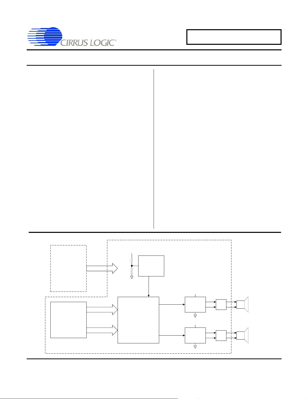
The CRD44600-PH-FB PWM Amplifier demonstrates
the CS44600, Cirrus’ multi-channel pure digital PWM
I
controller. This reference design implements a twochannel amplifier which delivers 100 W per full-bridge
channel into 8 Ω loads using a single +50 V supply (at
1% THD+N). A 155 W unregulated linear power supply
is used to power the CRD44600-PH-FB.
As shown below, the CS44600 IC takes two stereo digital audio PCM inputs and converts them to PWM
outputs. This 64-pin LQFP PWM controller provides an
integrated sample rate converter for 32 kHz-192 kHz input sample rate support, volume up/down, speaker load
compensation, peak limiting to prevent amplifier clipping,
power supply ripple compensation, and AM frequency
interference elimination.
This reference design uses the the Philips TDA8939, an
integrated power stage back end for digital amplifiers
(two TDA8939 parts configured as full-bridges are used
for this two-channel design). Current limiting and thermal protection are provided by the TDA893 9.
The inductor/capacitor 2
nd
order low pass filter (LPF) removes high frequency components from the output
signal effectively converting it from digital to analog.
ORDERING INFORMATION
CRD44600-PH-FB Reference Design
155W Unregulated
Linear Power Supply
Audio Inputs and GUI
Cirrus Logic, Inc.
www.cirrus.com
Interface
+50 V
PCM Clocks & Data
I2C Host Control
PSR Circuitry
+50 V
CS4461 ADC
Channel 1
CS44600
(PWM Controller)
Channel 2
Copyright © Cirrus Logic, Inc. 2005
(All Rights Reserved)
+50 V
Philips
TDA8939
+50 V
Philips
TDA8939
LPF
LPF
8Ω
8Ω
MAR '05
DS633RD1
1
Page 2

TABLE OF CONTENTS
1. SYSTEM OVERVIEW ............................................................................................................... 3
1.1 CS44600 PWM Modulator ................................................................................................. 3
1.2 CS4461 PSR Feedback ADC ................................. ... ... ... .... ... ... ... ... .... ... ... ........................3
1.3 TDA8939 Power Stage ....................... ... .... ... .......................................... ... ... .... ... ... ...........3
1.4 CS8416 Digital Audio Receiver .......................................................................................... 3
1.5 CS5341 Analog to Digital Converter ..................................................................................3
1.6 Control Port Interface and GUI .......................................................................................... 4
1.7 Unregulated Linear Power Supply ..................................................................................... 4
2. GUI CONTROL ......................................................................................................................... 5
2.1 CS44600 Dialog Tab .......................................................................................................... 5
2.2 Advanced Register Debug Tab .. ... ... ... ... .... .......................................... ... ... ... .... ... ... ... ... .... . 6
3. POWER SUPPLY ..................................................................................................................... 8
3.1 Power Supply Ratings ................................... ... ... .... ... ... ... .... ... ... ... .....................................8
3.2 Power Supply Decoupling ...... .... ... ... ... ... .... .......................................... ... ... ... .... ... ... ... ... .... . 8
4. ELECTROMAGNETIC INTERFERENCE (EMI) ....................................................................... 9
4.1 Suppression of EMI at the Source ..................................................................................... 9
4.2 EMI Testing ......... .......................................... ... ... .......................................... .... ... ... ...........9
5. CRD44600-PH-FB SCHEMATICS .........................................................................................14
6. CRD44600-PH-FB POWER SUPPLY SCHEMATICS ........................................................... 19
7. CRD44600-PH-FB LAYOUT ...................................................................................................20
8. CRD44600-PH-FB BILL OF MATERIALS ....................................................................... 23
9. TYPICAL PERFORMANCE PLOTS ....................................................................................... 25
10. REVISION HISTORY ............................................................................................................30
CRD44600-PH-FB
LIST OF FIGURES
Figure 1. CS44600 Dialog Tab........................................................................................................ 5
Figure 2. Advanced Register Debug Tab - CS44600......................................................................6
Figure 3. Advanced Register Debug Tab - CS8416........................................................................7
Figure 4. EMI Testing Setup..........................................................................................................11
Figure 5. EMI Testing Setup, Close-up .........................................................................................11
Figure 6. Radiated EMI Testing Results- 30 MHz to 200 MHz.......................................... ... ... ... ... 12
Figure 7. Radiated EMI Testing Results- 200 MHz to 1 GHz........................................................12
Figure 8. Conducted Power Line Testing Results.........................................................................13
Figure 9. Audio Inputs...................................................................................................................14
Figure 10. CS44600......................................................................................................................15
Figure 11. PSR Feedback.............................................................................................................16
Figure 12. Left/Right Channels......................................................................................................17
Figure 13. Control Port and Power................................................................................................18
Figure 14. Power Supply...............................................................................................................19
Figure 15. Silk Screen Top............................................................................................................ 20
Figure 16. Topside Layer .............................................................................................................. 21
Figure 17. Bottomside Layer .........................................................................................................22
Figure 18. Frequency Response...................................................................................................25
Figure 19. THD+N vs. Frequency at 1 W, 10 W, and 50 W ..........................................................26
Figure 20. THD+N vs. Power at 1 kHz..........................................................................................27
Figure 21. FFT at -60 dBFS and 1 kHz .........................................................................................28
Figure 22. FFT at -1 dBFS and 1 kHz. Red = PSR Feedback Off. Blue = PSR Feedback On .....29
LIST OF TABLES
2 MAR '05 DS633RD1
Page 3

CRD44600-PH-FB
Table 1. Bill of Materials................................................................................................................ 23
Table 2. Revision History.............................................................................................................. 30
MAR '05 DS633RD1 3
Page 4

CRD44600-PH-FB
1. SYSTEM OVERVIEW
The CRD44600-PH-FB reference design is an excellent means for evaluating the CS44600 sixchannel Class-D PWM modulator. It incorporates a digital Class-D PWM modulator, two fullbridge power stages, and power supply rejection (PSR) circuitry, all on a two-layer board.
The CRD44600-PH-FB schematic set is shown in Figures 9 through 13 and the board layout is
shown in Figures 15 through 17.
1.1 CS44600 PWM Modulator
A complete description of the CS44600 is included in the CS44600 product data sheet.
The CS44600 converts linear PCM data to pulse width modulated (PWM) output. It uses a
Sample Rate Converter (SRC) to eliminate serial audio interface jitter effects and maintains
a constant PWM switch rate of 384 kHz, resulting in high-quality sound output.
PCM data and clocks are input from either the CS8416 (S/PDIF Receiver), CS5341 (Stereo
ADC), or J19 (PCM Input Header).
1.2 CS4461 PSR Feedback ADC
A complete description of the CS4461 is included in the CS4461 product data sheet.
The CS4461 is connected to the CS44600 to provide power supply rejection (PSR) for the
VP supply voltage connected to J17. Resistors R41 and R42 are set for VP = +50 V. See the
CS4461 data sheet for equations to determine the resistor values.
1.3 TDA8939 Power Stage
A complete description of the Philips TDA8939 is included in the TDA8939 product data
sheet.
The TDA8939 is a high-voltage PWM amplifier power stage. It integrates two half-bridge drivers and fault protection. For the CRD44600-PH-FB, each of the two TDA8939’s are configured as full-bridges. Care should be taken to not connect the full bridge black speaker
connectors to ground as these outputs are driven.
1.4 CS8416 Digital Audio Receiver
The operation of the CS8416 receiver and a discussion of the digital audio interface are described in the CS8416 data sheet.
The CS8416 converts the input S/PDIF data stream into PCM data for the CS44600. The
CS8416 operates in master mode with RMCK = 256*Fs. The digital Interface format is set to
Left Justified (24-bit).
D20 (RERR) indicates a receiver error, such as loss of lock.
S/PDIF input is through OPT1 or J33.
1.5 CS5341 Analog to Digital Converter
The operation of the CS5341 ADC is described in the CS5341 data sheet.
4 MAR '05 DS633RD1
Page 5

CRD44600-PH-FB
The CS5341 converts analog audio into PCM data for the CS44600. The CS5341 operates
in slave mode and the digital Interface format is set to Left Justified (24-bit).
Analog input is through J5 and J6.
1.6 Control Port Interface and GUI
The CS44600 and CS8416 are controlled through the provided control port interface. Connection to the control port is made through J37 (RS-232 Serial). A Windows based GUI provides control over all the individual registers of the CS44600 and the CS8416.
1.7 Unregulated Linear Power Supply
The power supply used for the CRD44600-PH-FB is a linear 155 W supply. The supply provides an unregulated +50 V for the TDA8939 power stages. The power supply consists of a
transformer, diode bridge rectifier, and bulk capacitor. Schematics are shown in Figure 14.
MAR '05 DS633RD1 5
Page 6
CRD44600-PH-FB
2. GUI CONTROL
The CRD44600-PH-FB is shipped with a Microsoft Windows® based GUI, which allows control
over the CS8416 and CS44600 registers. Interface to the CDB44600 control port is provided using an RS-232 serial cable. The GUI requires no installation and can be run directly from the CD
or copied to a local directory and run from there. Once the serial port cable is connected between
the CRD44600-PH-FB and the host PC, load the FlexLoader.exe from the CRD44600-PH-FB directory. Once loaded, all registers are set to their default reset state. The GUI File menu provides the ability to save and restore (load) register settings. Sample script files are provided for
basic functionality. The GUI serial port interface is setup by default for 115.2 Kbps operation on
COM1. To change these settings, edit the “CRD44600-PH-FBCommunications” section of the
flexconfig.ini file or change the system communications setting in the Windows® control panel.
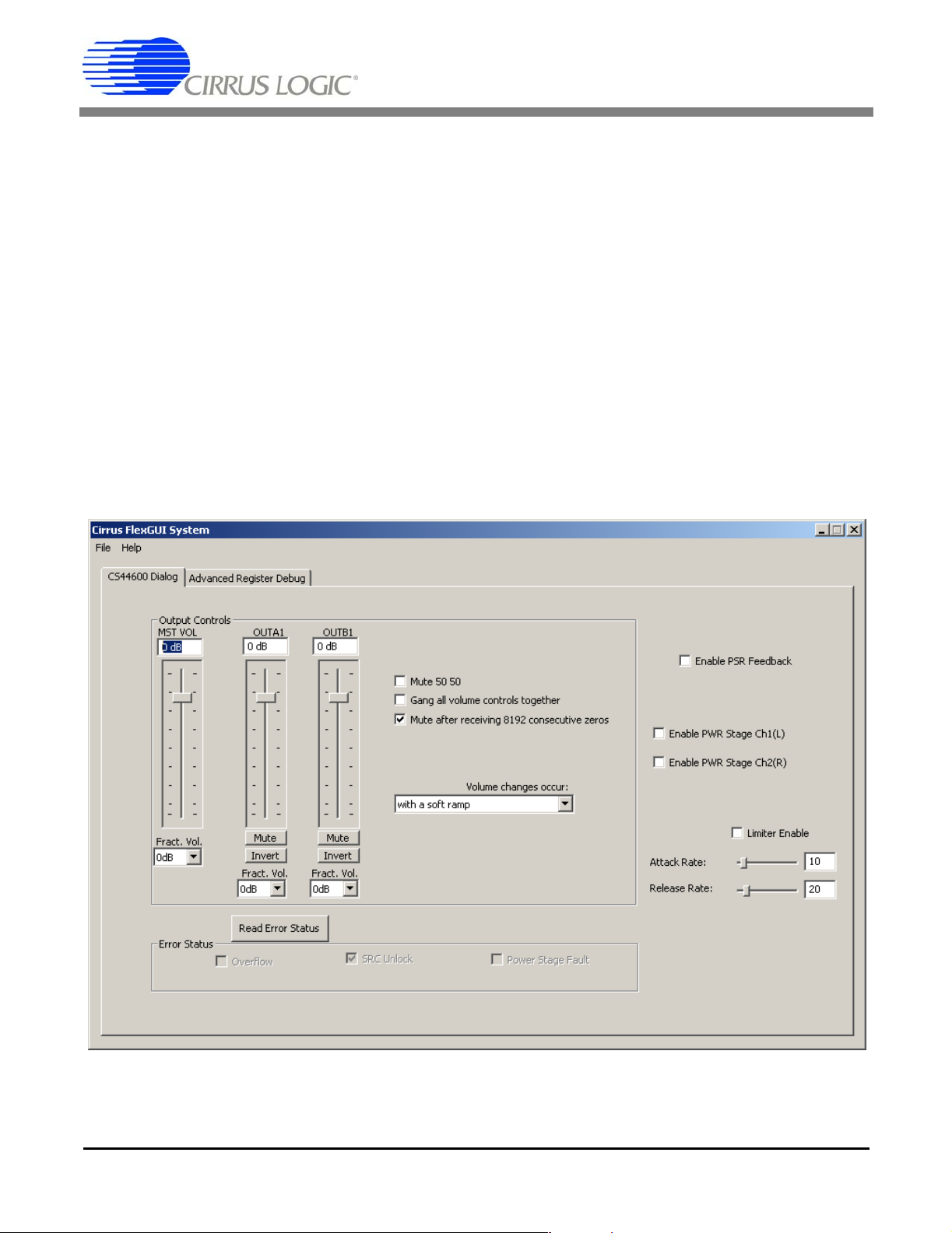
2.1 CS44600 Dialog Tab
The CS44600 Dialog tab provides high level control over the CS44600’s registers. Controls
are provided to change volume, mute, enable PSR, enable the power stages, limiter control.
Figure 1. CS44600 Dialog Tab
6 MAR '05 DS633RD1
Page 7
CRD44600-PH-FB
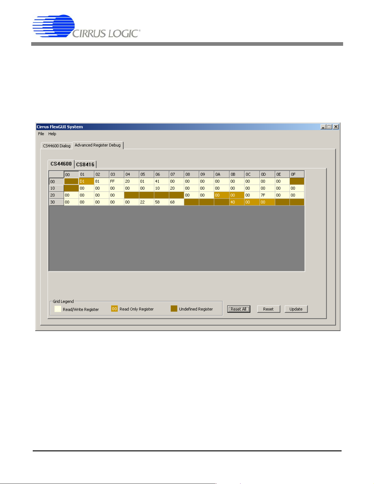
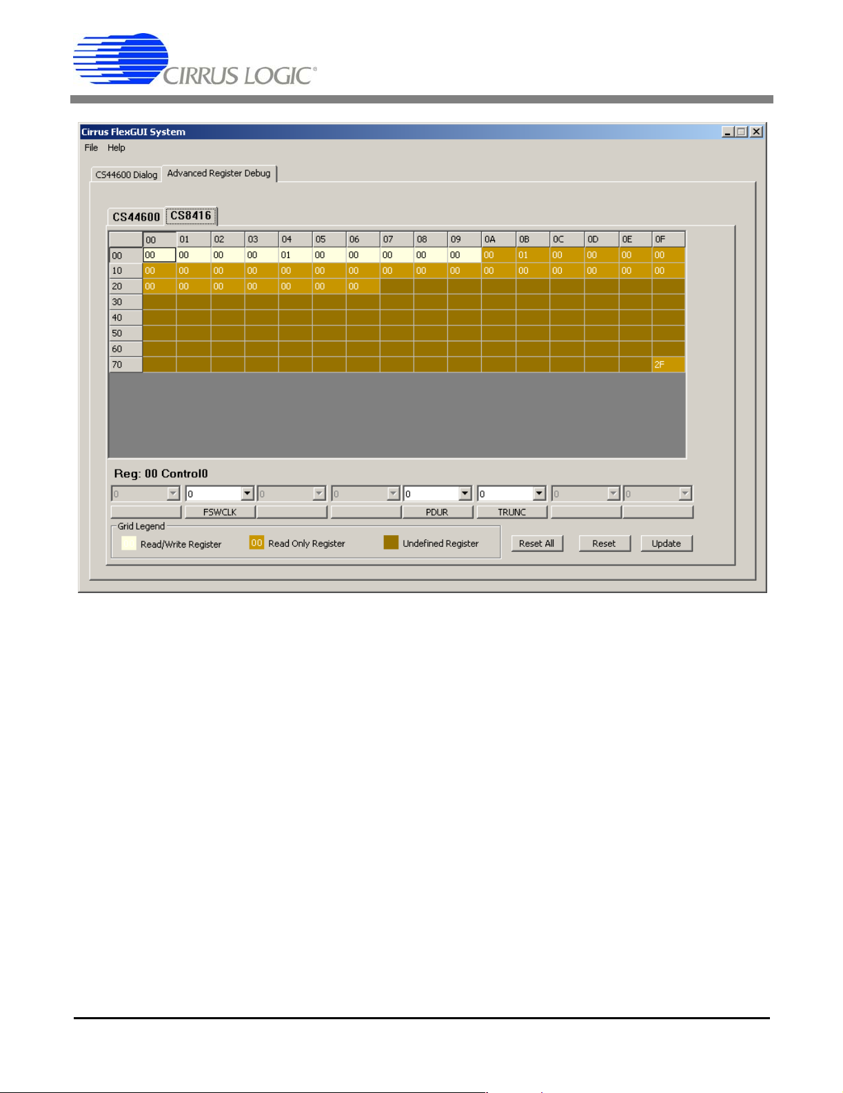
2.2 Advanced Register Debug Tab
The Advanced Register Debug tab provides low level control over the CS44600 and CS8416
individual register settings. Each device is displayed on a separate tab. Register values can
be modified bitwise or bytewise. For bitwise, click the appropriate push button for the desired
bit. For bytewise, the desired hex value can be typed directly in the register address box in
the register map.
Figure 2. Advanced Register Debug Tab - CS44600
MAR '05 DS633RD1 7
Page 8
CRD44600-PH-FB
Figure 3. Advanced Register Debug Tab - CS8416
8 MAR '05 DS633RD1
Page 9

CRD44600-PH-FB
3. POWER SUPPLY
3.1 Power Supply Ratings
The required power supply current rating can be estimated as follows. 95 W is used as the
reference output power per channel because this represents the typical full scale output with
no clipping. Assume the efficiency, η, is approximately 85% (this accounts for power to supply control electronics and overhead), then for 95 W x 2 channels:
WP
190
Total
P
Supply
P
Consequently the supply current is:
Out
224
85.0
W
2
η
Total
P
2
W
224
===
W
112
===
Supply
I
Supply
P
V
Supply
The factor of 2 in the denominator of the P
Supply
W
112
50
===
V
A
24.2
calculation arises from the fact that for typical
consumer applications in A/V or DVD receivers, the power supply should be capable of providing ½ the total requirement for all channels operating at full power. This design guide is
still quite conservative, and gives more than adequate headroom in real applications.
3.2 Power Supply Decoupling
Proper power supply decoupling is one key to maximizing the performance of a Class-D amplifier. Because the design uses an open loop output stage, noise on the power supply rail
will be coupled to the output. While the PSR functionality of the CS44600 helps reduce power
supply noise feedthrough to the output, careful decoupling of the power stage supply rails is
essential. Referring to Figure 15, the top side of the CRD44600-PH-FB PWM amplifier board,
good decoupling practice is shown. Notice that the 0.1 µF ceramic capacitors are as close
as physically possible to the power pins of the TDA8939. The ground side of the capacitors
is connected directly to top side ground plane, which is also used by the power supply return
pins. This keeps the high frequency current loop small to minimize power supply variations
and EMI. 470 µF electrolytic capacitors are also located in close proximity to the power supply pins to supply the current locally for each channel. These are not required to be expensive
low ESR capacitors. General purpose electrolytic capacitors that are specified to handle the
ripple current can be used. The real time PSR feedback of the CS44600/CS4461 can greatly
attenuate the induced voltages due to the power supply ripple current.
MAR '05 DS633RD1 9
Page 10

CRD44600-PH-FB
4. ELECTROMAGNETIC INTERFERENCE (EMI)
This reference design from Cirrus Logic is a board level solution which is meant to control
emissions by minimizing and suppressing them at the source in contrast to containing them
in an enclosure. Utilizing spread spectrum modulation techniques to reduce the overall
switching energy, along with a low internal modulator clock frequency of 24.576 MHz, the radiated emissions are greatly reduced. These features allow for the use of very low cost components to couple the high frequency noise to chassis ground. No common mode chokes,
inductors, or power line filters were required.
The EMI requirements for an amplifier have added dimensions beyond those imposed on
power supplies. Audio amplifiers are usually located in close proximity to radio receivers, particularly AM receivers which are notoriously sensitive to interference. Amplifiers also need to
operate with speaker leads of unpredictable length and construction which make it possible
for any high frequency currents that appear on the outputs to generate nuisance emissions.
4.1 Suppression of EMI at the Source
Several techniques are used in the circuit design and board layout to minimize high frequency fields in the immediate vicinity of the high power components. Specific techniques
include the following:
• As was mentioned in Section 3.2, effective power supply decoupling of high frequency currents, and minimizing the loop area of the decoupling loop is one aspect of minimizing EMI.
• Each output of the TDA8939 includes “snubbing” components. For example, OUT1 of U1 includes snubber components R18/R30 (5.6 Ω) and C34/C46 (560 pF). These components serve
to damp ringing on the switching outputs in the 30-50 MHz range. The snubbing components
should be as close as practical to the output pins to maximize their effectiveness. Again, refer
to Figure 15 for the preferred component layout.
• A separate ground plane with a capacitively coupled electrical connection to the chassis and
which surrounds the speaker output connector should be implemented. This allows the speaker
outputs to be AC coupled to the chassis just before they exit the chassis from the speaker connector. Again, refer to Figure 15 for the preferred component layout.
• Make use of source termination resistors on all digital signals whose traces are longer than approximately 25 mm.
It is extremely critical that the layout of the power amplifier section of the Cirrus Logic
CS44600 Reference Design be copied as exactly as possible to assure best RF/EMI performance.
4.2 EMI Testing
The CRD44600-PH-FB has been tested to CISPR and FCC Class B limits for radiated and
power line conducted emissions. The same test setup and test signal were used for all
tests. The setup consisted of an unregulated linear power supply, CRD44600-PH-FB
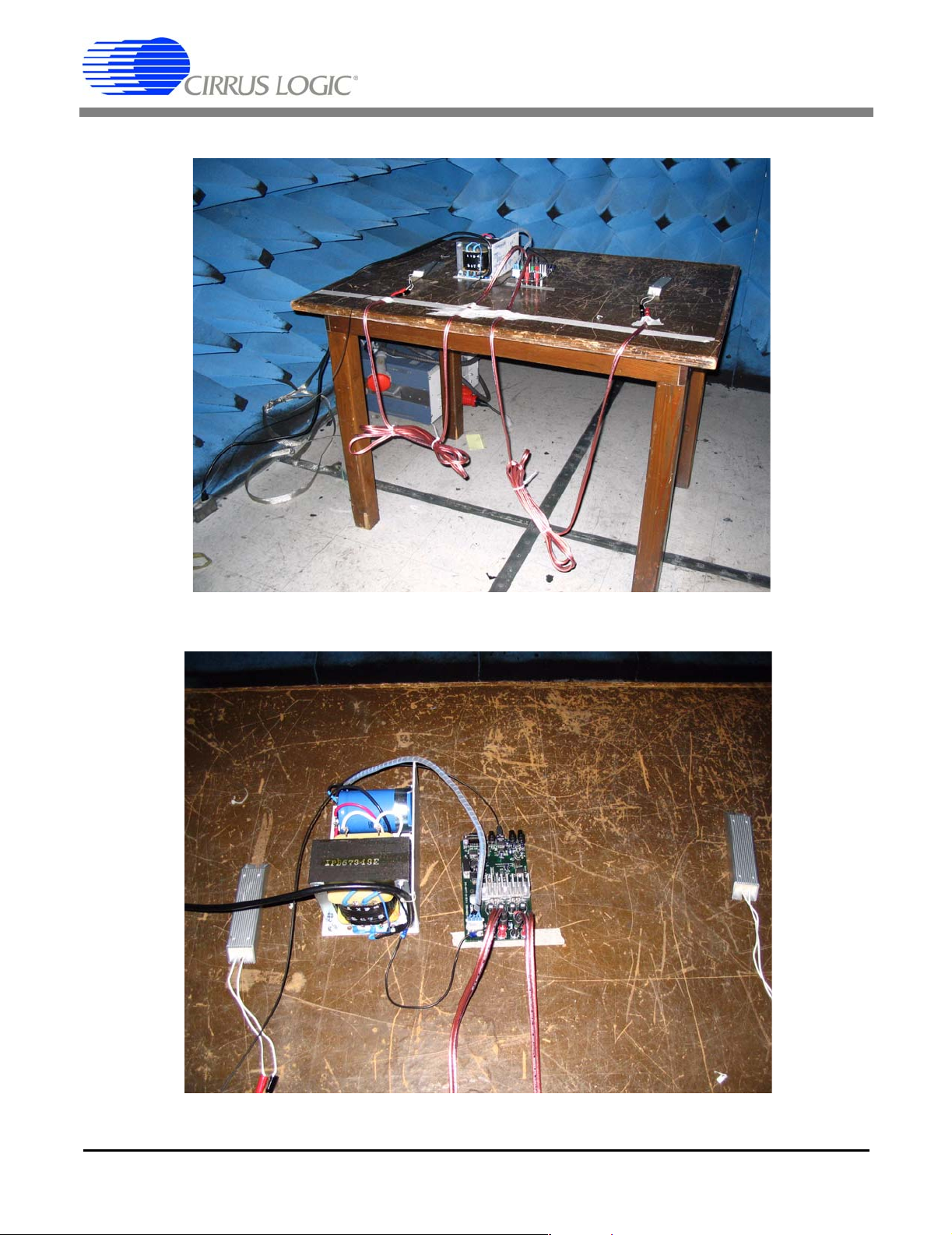
board, 5m of speaker cable, and two 8-Ω resistive loads. This setup is shown in Figure 4
10 MAR '05 DS633RD1
Page 11

CRD44600-PH-FB
and Figure 5. The power supply earth ground was connected to the board chassis ground
at a single point.
A CD-player with an optical fiber connection was used a signal source. A constant 0dBFS, 1-kHz sine wave was used as the test signal and the board volume was set so that
the output to the resistive loads was 1/8th of the full scale output level, or 12.5 W.
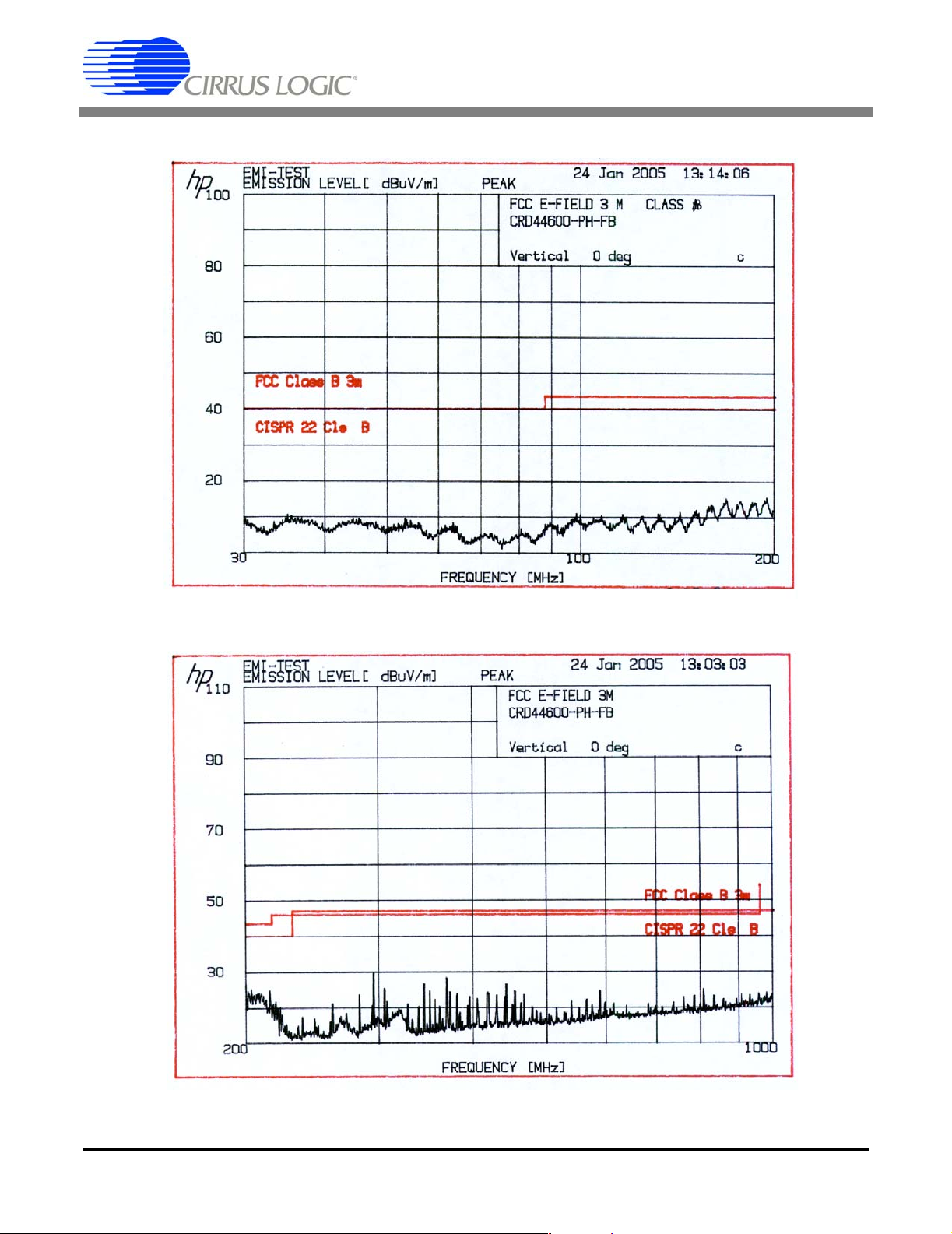
The test results shown in Figure 6 and Figure 7 are pre-screened radiated EMI test results
from an antenna placement of 3 m in an anechoic chamber. The test results shown in Figure 8 are preliminary power line conducted test results.
MAR '05 DS633RD1 11
Page 12
CRD44600-PH-FB
Figure 4. EMI Testing Setup
Figure 5. EMI Testing Setup, Close-up
12 MAR '05 DS633RD1
Page 13
CRD44600-PH-FB
Figure 6. Radiated EMI Testing Results- 30 MHz to 200 MHz
Figure 7. Radiated EMI Testing Results- 200 MHz to 1 GHz
MAR '05 DS633RD1 13
Page 14

CRD44600-PH-FB
Figure 8. Conducted Power Line Testing Results
14 MAR '05 DS633RD1
Page 15

5. CRD44600-PH-FB SCHEMATICS
CRD44600-PH-FB
Figure 9. Audio Inputs
MAR '05 DS633RD1 15
Page 16

CRD44600-PH-FB
Figure 10. CS44600
16 MAR '05 DS633RD1
Page 17

CRD44600-PH-FB
Figure 11. PSR Feedback
MAR '05 DS633RD1 17
Page 18

CRD44600-PH-FB
Figure 12. Left/Right Channels
18 MAR '05 DS633RD1
Page 19

CRD44600-PH-FB
Figure 13. Control Port and Power
MAR '05 DS633RD1 19
Page 20

6. CRD44600-PH-FB POWER SUPPLY SCHEMATICS
CRD44600-PH-FB
Figure 14. Power Supply
20 MAR '05 DS633RD1
Page 21

7. CRD44600-PH-FB LAYOUT
CRD44600-PH-FB
Figure 15. Silk Screen Top
MAR '05 DS633RD1 21
Page 22

CRD44600-PH-FB
Figure 16. Topside Layer
22 MAR '05 DS633RD1
Page 23

CRD44600-PH-FB
Figure 17. Bottomside Layer
MAR '05 DS633RD1 23
Page 24

8. CRD44600-PH-FB BILL OF MATERIALS
p
y
g
r
L
PANASONIC ECJ1VC1H102J
MFG MFG P/N
KEMET C1206C104K1RAC
KEMET C0603C104K4RAC
CRD44600-PH-FB
nato
C167 C173 C174 C205 C208 C210
Refe rence Desi
tion Qt
1 CAP 1000pF ±5% 50V C0G 0603 21 C1 C2 C4 C9 C10 C11 C12 C56 C71 C72 C73 C83 C88 C89 C153
2 NO POP CAP 0603 0 C3 C20 C21 C22 C78 C79 NO POP NP-CAP-0603
3 CAP 0.22uF ±5% 50V X7R 1206 4 C5 C6 C7 C8 KEMET C1206C224J5RAC
Item Descri
4 CAP 0.01uF ±10% 50V X7R 0603 10 C13 C84 C90 C91 C92 C93 C94 C95 C195 C196 KEMET C0603C103K5RAC
C110 C111 C112 C113
5 CAP 0.68µF ±10% 100V POLY RAD 2 C14 C16 PANASONIC ECQE1684KF
6 CAP 0.1uF ±10% 100V X7R 1206 18 C15 C19 C61 C62 C67 C68 C69 C70 C80 C81 C82 C85 C86 C87
7 CAP 100uF ±20% 10V ELEC RAD 5X11 6 C17 C51 C76 C125 C214 C227 PANASONIC ECA1AM101
8 CAP 470pF ±5% 50V C0G 0603 2 C18 C23 KEMET C0603C471J5GAC
9 CAP 1uF ±10% 100V X7R 1210 4 C24 C25 C65 C66 MURATA GRM32ER72A105KA01
C126 C128 C129 C134 C156 C158 C159 C164 C166 C168 C170
C172 C175 C177 C180 C181 C194 C199 C201 C213 C221 C222
C230 C231 C232
10 NO POP CAP 0805 0 C26 C63 C64 C96 NO POP NP-CAP-0805
11 CAP 10uF ±20% 50V ELEC RAD 7 C27 C31 C54 C59 C182 C190 C219 PANASONIC ECA1HM100I
12 CAP 0.1uF ±10% 16V X7R 0603 39 C28 C32 C37 C40 C41 C43 C49 C50 C52 C55 C57 C60 C74 C124
13 CAP 470uF ±20% 63V ELEC RAD 2 C29 C30 PANASONIC ECA1JM471B
14 CAP 560pF ±5% 100V C0G 0805 8 C33 C34 C35 C36 C45 C46 C47 C48 KEMET C0805C561J1GAC
15 CAP 2200pF ±5% 50V C0G 0805 3 C38 C39 C130 KEMET C0805C222J5GAC
16 CAP 1uF ±10% 25V X7R 1206 5 C42 C44 C77 C127 C131 KEMET C1206C105K3RAC
17 CAP 0.01uF ±5% 25V C0G 1206 2 C53 C58 KEMET C1206C103J3GAC
18 CAP 10uF ±20% 63V ELEC RAD 5x11 1 C75 PANASONIC ECA1JM100I
19 CAP 120pF ±5% 50V C0G 0603 2 C122 C123 KEMET C0603C121J5GAC
20 CAP 0.022uF ±5% 50V X7R 0603 1 C215 KEMET C0603C223J5RAC
21 LED CLR SUP RED 1.7V 1mA 1.6MCD SMD 1 D20 CHICAGO MINIATURE CMD28-21SRC/TR8/T1
22 HTSNK 30W DUAL SITE 1 HS1 SUMMIT HEAT SINKS CO LTD 311-00005-01
23 CON BPOST 2" SILV NYLON INS RED 2 J1 J3 JOHNSON COMPONENTS 111-0102-001
24 CON BPOST 2" SILV NYLON INS BLK 2 J2 J4 JOHNSON COMPONENTS 111-0103-001
25 JACK RCA, RA-BLK, PHONO, GLD TABS 3 J5 J6 J33 A/D ELECTRONICS ARJ-2018-NIL-1-NIL
26 HDR 2x1 ML .1"CTR 062BD ST GLD TH 1 J7 SAMTEC TSW-102-07-G-S
27 CON PWR SHIELDED 4PIN 1 J17 MOLEX 15-24-4049
28 HDR 4x3 MLE .1"CTR S GLD 1 J19 SAMTEC TSW-104-07-G-T
29 HDR 5x2 MLE .1"CTR S GLD 1 J26 SAMTEC TSW-105-07-G-D
30 CON DSUB 9P FML .318"W W/ BDLCK RA 1 J37 AMP 747844-6
31 IND 22uH 6A ±10% 400 DIA TH 4 L1 L2 L3 L4 TRANSTEK MAGNETICS TMP50627CT
32 IND 47uH 20% CDRH125 SERIES SMT 1 L9 SUMIDA CDRH125-470MC
33 IND 680uH 20% CDRH125 SERIES SMT 1 L10 SUMIDA CDRH125-681MC
34 IND 47uH ±10% 1210 1 L16 PANASONIC ELJFA470KF
35 IND 4.7uH ±10% 0805 1 L17 PANASONIC ELJFD4R7KF
36 SPCR, STANDOFF 4-40 THR, 0.875"L 6 MH1 MH2 MH3 MH4 MH5 MH6 KEYSTONE 1809
Table 1. Bill of Materials
37 OPTICAL RCVR 6Mb/s 7V 20MA 10M 1 OPT1 TOSHIBA TORX173
38 RES 10k OHM 1/10W ±1% 0603 FILM 10 R1 R2 R3 R14 R15 R38 R74 R157 R169 R179 DALE CRCW06031002F
24 MAR '05 DS633RD1
Page 25

CRD44600-PH-FB
p
y
g
r
MFG MFG P/N
nato
Refe rence Desi
DALE CRCW060390R9F
R135 R140
tion Qt
Item Descri
39 RES 22.1 OHM 1/10W ±1% 0603 FILM 12 R4 R11 R72 R73 R93 R108 R154 R161 R162 R167 R172 R176 DALE CRCW060322R1F
40 RES 22.1 OHM 1W ±1% 2512 FILM 4 R5 R6 R7 R8 DALE CRCW251222R1F
41 RES 90.9 OHM 1/10W ±1% 0603 FILM 15 R12 R13 R26 R27 R62 R63 R94 R95 R96 R97 R131 R133 R134
42 RES 5.6 OHM 1W ±5% 2512 FILM 8 R17 R18 R19 R20 R29 R30 R31 R32 DALE CRCW25125R6J
43 RES 649 OHM 1/10W ±1% 0603 FILM 4 R24 R25 R60 R187 DALE CRCW06036490F
44 RES 100k OHM 1/10W ±1% 0603 FILM 6 R28 R33 R34 R35 R36 R37 DALE CRCW06031003F
45 RES 10 OHM 1/8W ±5% 0805 FILM 10 R39 R45 R46 R47 R48 R68 R106 R170 R180 R182 DALE CRCW0805100J
46 RES 2k OHM 1/10W ±1% 0603 FILM 5 R41 R51 R61 R98 R146 DALE CRCW06032001F
47 RES 54.9k OHM 1/10W ±1% 0603 FILM 1 R42 DALE CRCW06035492F
48 NO POP RES 0805 0 R111 NO POP NP-RES-0805
49 RES 1k OHM 1/10W ±5% 0603 FILM 3 R150 R151 R156 DALE CRCW0603102J
50 RES 75 OHM 1/10W ±1% 0603 FILM 1 R171 DALE CRCW060375R0F
51 RES 3.01k OHM 1/10W ±1% 0603 FILM 1 R178 DALE CRCW06033011F
52 IC LOG CLASS D PWR COMP HSOP24 2 U1 U2 PHILIPS TDA8939TH
53 IC LNR DUAL OP AMP LOW V RRO VSP8 2 U3 U4 NJR NJM2140R
54 IC CRUS, 105dB 192kHz M-BIT AUD ADC 1 U6 CIRRUS LOGIC CS5341-CZZ/E
55 IC LNR VREG µPWR 150mA 3.3V SOT23-5 1 U7 NATIONAL SEMICONDUCTOR LP2985IM5-3.3
56 IC CRUS A/D PSR FEEDBACK TSSOP24 1 U8 CIRRUS LOGIC CS4461-CZZ/D
57 IC LNR VREG µPWR 150MA 2.5V SOT23-5 1 U9 NATIONAL SEMICONDUCTOR LP2985IM5-2.5
58 IC LNR ISO 2W SINGLE OUT DC-DC CONV 1 U10 C&D TECHNOLOGIES NDL4805S
59 IC CRUS 6-CH DIG AMP CTRL LQFP64 1 U14 CIRRUS LOGIC CS44600-CQZ/A
60 IC LOG, UHS 2IN NON INV MUX SC70-6 1 U17 FAIRCHILD SEMICONDUCTOR NC7SZ157P6X
61 IC PGM USB 16kB FLASH MCU LQFP32 1 U20 CYGNAL C8051F320
62 IC CRUS 192kHz DIG AUD RCVR TSSOP28 1 U26 CRYSTAL SEMICONDUCTOR CS8416-CZ/E
63 IC LNR 5V RS-232 DRV/RCVR SO16-300 1 U31 MAXIM MAX232ACWE
64 IC PGM 128 BIT SER EEPROM SOT23-5 1 U32 MICROCHIP 24LC00-I/OT
65 OSC 24.576MHz 50PPM 5V HALF DIP8 1 Y2 CAL CRYSTAL CX21AH-24.576MHZ
65 WIRE, HOOK-UP 12AWG 65/30 RED 100ft 4 XJ1 XJ2 XJ3 XJ4 ALPHA WIRE COMPANY 3080 RD005
66 SCREW 4-40X5/16" PH STEEL 6 XMH1 XMH2 XMH3 XMH4 XMH5 XMH6 BUILDING FASTENERS PMS 440 0031 PH
67 SCREW 4-40X1/4"L PH STEEL 3 XHS1 McMASTER-CARR 90190A106
68 WASHER LOCK INTERNAL #4 3 XHS1 BUILDING FASTENERS INT LWZ 004
MAR '05 DS633RD1 25
Page 26

CRD44600-PH-FB
9. TYPICAL PERFORMANCE PLOTS
These performance plots were taken with the CRD44600-PH-FB powered from the described
+50 V linear unregulated power supply. The PSR circuitry was calibrated to a nominal +50 V rail.
+1
+0.5
-0
-0.5
-1
-1.5
-2
-2.5
-3
-3.5
-4
-4.5
-5
Hz
Figure 18. Frequency Response
20 20k50 100 200 500 1k 2k 5k 10k
B
r
A
d
26 MAR '05 DS633RD1
Page 27
1
CRD44600-PH-FB
0 W
W
0 W
Hz
Figure 19. THD+N vs. Frequency at 1 W, 10 W, and 50 W
1
0.5
0.2
0.1
0.05
0.02
0.01
0.005
0.002
20 20k50 100 200 500 1k 2k 5k 10k
0.001
%
MAR '05 DS633RD1 27
Page 28

CRD44600-PH-FB
10
5
2
1
0.5
0.2
0.1
0.05
0.02
W
Figure 20. THD+N vs. Power at 1 kHz
100m 100200m 500m 1 2 5 10 20 50
0.01
%
28 MAR '05 DS633RD1
Page 29

CRD44600-PH-FB
+0
-10
-20
-30
-40
-50
-60
-70
-80
-90
-100
-110
-120
-130
Hz
Figure 21. FFT at -60 dBFS and 1 kHz
20 20k50 100 200 500 1k 2k 5k 10k
-140
B
r
A
d
MAR '05 DS633RD1 29
Page 30

CRD44600-PH-FB
+0
-10
-20
-30
-40
-50
-60
-70
-80
-90
-100
-110
-120
-130
Hz
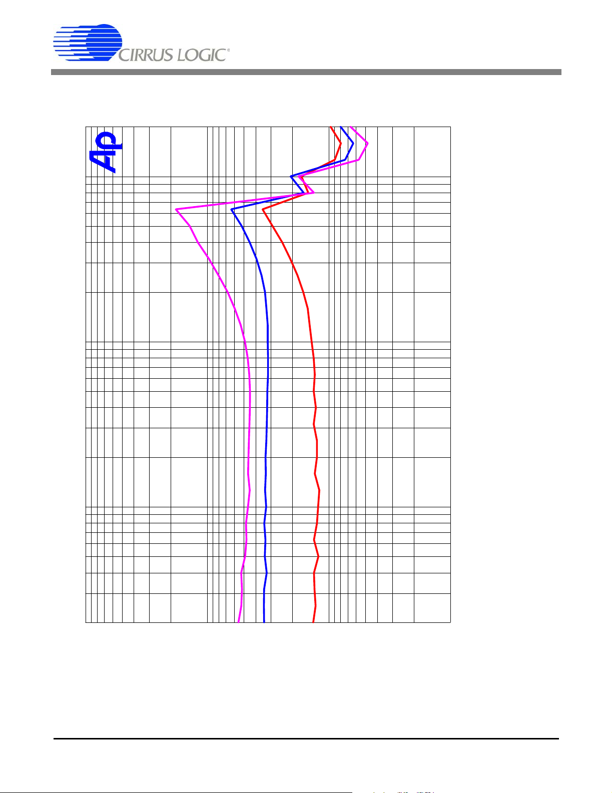
Figure 22. FFT at -1 dBFS and 1 kHz. Red = PSR Feedback Off. Blue = PSR Feedback On
20 20k50 100 200 500 1k 2k 5k 10k
-140
B
r
A
d
30 MAR '05 DS633RD1
Page 31

10. REVISION HISTORY
Release Date Changes
RD1 March 2005 1st Release
CRD44600-PH-FB
Table 2. Revision History
Contacting Cirrus Logic Support
For all product questions and inquiries contact a Cirrus Logic Sales Representative.
To find one nearest you go to <http://www.cirrus.com/corporate/contacts/sales.cfm>
IMPORTANT NOTICE
Cirrus Logic, Inc. and it s su bsi di ar i es ( " Ci r ru s" ) bel i eve that the information conta i ned in t hi s doc ument is accurate and reli able . Howev er , t he in f ormation is subject
to change without not ice and i s provi ded "AS I S" witho ut warrant y of an y kind ( express o r implie d). Cust omers are a dvised t o obtain the latest version of relevant
information to verify, before placing orders, that information being relied on is current and complete. All products are sold subject to the terms and conditions of sale
supplied at the time of order acknowledgment, including those pertaining to warranty, indemnification, and limitation of liability. No responsibility is assumed by Cirrus
for the use of this information, includ ing u se of this i nforma tion a s the basis for m anu facture or sa le of a ny item s, or for in fringement of patents or other rights of third
parties. This document is the property of Cirru s and by furnishing this information, Cirrus grants n o lice nse, express or implied under any patents, mask work rights,
copyrights, trademarks, trade secrets or other intellectual property rights. Cirrus owns the copyrights associated with the information contained herein and gives consent for copies to be made of the information only for use within your organization with respe c t to Cirrus integrated circu its or other products of Cirrus. This consent
does not extend to other copying such as copying for general distribution, advertising or promotiona l purposes, or for creating any work for resale.
CERTAIN APPLICATIONS USING SEMI CONDUCTOR P RODUCT S MAY I NVOL VE PO TENT I AL RI SKS OF DEAT H, PE RS ONAL IN JU RY, OR S EV ERE PRO PERTY OR ENVIRONMENTAL DAMAGE (“CRITICAL APPLICATIONS”). CIRRUS PRODUCTS ARE NOT DESIGNED, AUTHORIZED OR WARRANTED FOR USE
IN AIRCRAFT SYSTEMS, MILITARY APPLICATIONS, PRODUCTS SURGICALLY IMPLANTED INTO THE BODY, AUTOMOTIVE SAFETY OR SECURITY DEVICES, LIFE SUPPORT PRODUCTS OR OTHER CRITICAL APPLICATIONS. INCLUSION OF CIRRUS PRODUCTS IN SUCH APPLICATIONS IS UNDERSTOOD
TO BE FULLY AT THE CUSTOMER’S RISK AND CIRRUS DISCLAIMS AND MAKES NO WARRANTY, EXPRESS, STATUTORY OR IMPLIED, INCLUDING THE
IMPLIED WARRANTIES OF MERCHANTABILITY AND FITNESS FOR PARTICULAR PURPOSE, WITH REGARD TO ANY CIRRUS PRODUCT THAT IS USED
IN SUCH A MANNER. IF THE CUSTOMER OR CUSTOMER’S CUSTOMER USES OR PERMITS THE USE OF CIRRUS PRODUCTS IN CRITICAL APPLICATIONS, CUSTOMER AGREES, BY SUCH USE, TO FULLY INDEMNIFY CIRRUS, ITS OFFICERS, DIRECTORS, EMPLOYEES, DISTRIBUTORS AND OTHER
AGENTS FROM ANY AND ALL LIABILITY, INCLUDING ATTORNEYS’ FEES AND COSTS, THAT MAY RESULT FROM OR ARISE IN CONNECTION WITH
THESE USES.
Cirrus Logic, Cirrus, and the Cirrus Log ic lo go d esi gn s ar e trademarks of Cirrus Logic, Inc. All other brand an d pr od uct names in this document may be trademarks
or service marks of their respective owners.
Microsoft Windows is a registered trademark of Microsoft Corporation.
MAR '05 DS633RD1 31
Page 32

CRD44600-PH-FB
32 MAR '05 DS633RD1
 Loading...