

Page 1
CRD42L52
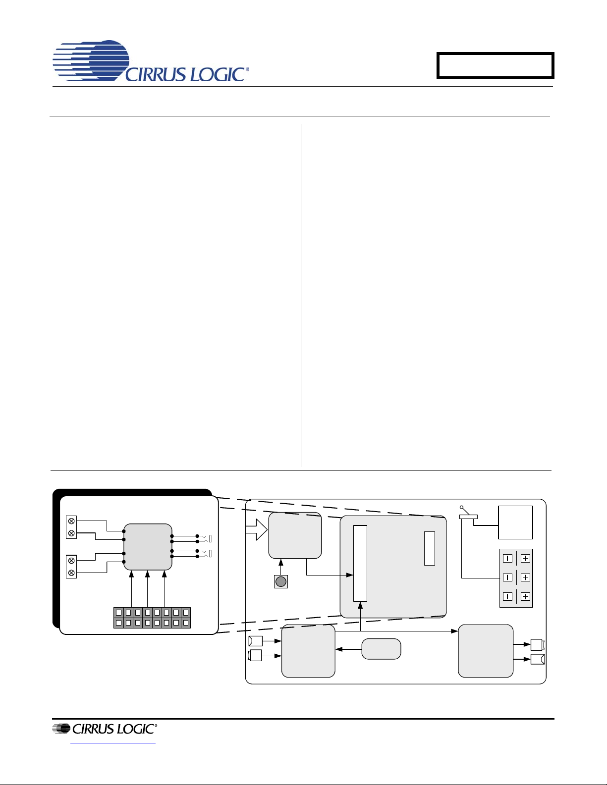
Reference Design and Peripheral Driver Board for CS42L52
Reference Design Board (CRD42L52)
Features
Ultra-Small Layout
Stake Header for External System Connections
1/8” Stereo Input Allows up to 2 Vrms Signals
1/8” Stereo Headphone Output Jack
Built-in Switch Control for CS42L52 SPKR/HP
Pin
Stereo Full Bridge Speaker Output Terminal
Complies with FCC class B and CISPR 22
Standards for Radiated Emissions
Peripheral Driver Board (CDB42LDB1)
Features
Multiple Power Supply Options
– Three AAA Battery Source
– External Power Supply Header
S/PDIF I/O (CS8416 Receiver)
– Optical and RCA Input Jacks
S/PDIF I/O (CS8406 Transmitter)
– Optical and RCA Output Jacks
FlexGUI S/W Control - Windows
– Pre-Defined & User Configurable Scripts
®
Compatible
Description
In addition to providing a reference for an ultra small layout design, the purpose of the CRD42L52 is to allow a
quick and easy evaluation of the CS42L52 low power
stereo CODEC.
Two 1/8” stereo jacks on the CRD42L52 provide an interface for analog line-level input and headphone-level
output connections to the CS42L52. Stereo differential
PWM speaker outputs from the CS42L52 can be monitored on a pair of screw term inals on the CRD42L52.
The control port and serial audio interfaces are accessible via the I/O stake header used to attach the
CRD42L52 to the CDB42LDB1.
The CDB42LDB1 is a peripheral driver board that provides clock/data, control logic and power supply to the
CRD42L52. Digital data is transmitted and received via
S/PDIF optical and RCA connectors. The CRD42L52
can be programmed by using the Windows Compatible
FlexGUI software provided. Power is derived either
from three AAA batteries or from an external supply on
the CDB42LDB1 driver board and is routed to the
CRD42L52 via the I/O stake header.
ORDERING INFORMATION
CRD42L52 Reference Design
CDB42LDB1 Driver Board
Speaker
Left
Right
+
+
-
-
Control
Port
J5
CRD42L52
CS42L52
I²C
http://www.cirrus.com
Line
Input
Headphone
Output
Power
SAI
Supply
USB
Micro Reset
Pushbutton
S/PDIF
Input
Microcontroller
I²C Control Port
Interface
S/PDIF Rx
CS8416
MCLK
J3
I/O Header
Serial Audio Interface
12.288 MHz
CRD
Placeholder
J4
AAA Battery
S/PDIF Tx
Clip
CS8406
External
Power
S/PDIF
Output
CDB42LDB1
Copyright © Cirrus Logic, Inc. 2008
(All Rights Reserved)
APRIL '08
DS680RD1
Page 2

TABLE OF CONTENTS
1. SYSTEM OVERVIEW ............................................................................................................................. 4
1.1 Power (U2) ....................................................................................................................................... 4
1.2 Microcontroller (U3) ......................................................................................................................... 4
1.3 CS8416 Digital Audio Receiver (U7) ................................................................................................ 4
1.4 CS8406 Digital Audio Transmitter (U8) ............................................................................................ 4
1.5 Oscillator (Y1) .................................................................................................................................. 5
1.6 CS42L52 Audio CODEC (U1) .......................................................................................................... 5
1.7 Analog Input ..................................................................................................................................... 5
1.8 Analog Outputs ................................................................................................................................ 5
1.9 Layout .............................................................................................................................................. 5
2. QUICK-START GUIDE ........................................................................................................................... 6
3. CONFIGURATION OPTIONS ................................................................................................................. 7
3.1 S/PDIF In to Headphone Out ........................................................................................................... 7
3.2 Line In to S/PDIF Out ....................................................................................................................... 7
3.3 S/PDIF In to Speaker Out ................................................................................................................ 8
3.4 Analog In to Analog Out - Digital Loopback ..................................................................................... 8
4. SOFTWARE MODE CONTROL ............................................................................................................. 9
4.1 CODEC Configuration Tab ............................................................................................................ 10
4.2 Analog Input Volume Tab .............................................................................................................. 11
4.3 DSP Engine Tab ............................................................................................................................ 12
4.4 Analog and PWM Output Volume Tab ...........................................................................................13
4.5 Register Maps Tab ......................................................................................................................... 14
5. PERFORMANCE PLOTS ..................................................................................................................... 15
6. SYSTEM CONNECTIONS & INTERFACE ........................................................................................... 18
CRD42L52 AND CDB42LDB1 BLOCK DIAGRAM .............................................................................. 19
7. CRD42L52 SCHEMATICS ................................................................................................................... 20
8. CDB42LDB1 SCHEMATICS ................................................................................................................ 21
9. CRD42L52 LAYOUT ............................................................................................................................ 23
10. CDB42LDB1 LAYOUT ....................................................................................................................... 24
11. REVISION HISTORY .......................................................................................................................... 27
CRD42L52
2 DS680RD1
Page 3

LIST OF FIGURES
Figure 1.Quick-Start Guide ......................................................................................................................... 6
Figure 2.CRD42L52 and CDB42LDB1 Block Diagram for ADC and DAC Testing ..................................... 7
Figure 3.CRD42L52 and CDB42LDB1 Block Diagram for Digital Loopback Testing .................................. 8
Figure 4.CODEC Configuration Tab ......................................................................................................... 10
Figure 5.Analog Input Volume Tab ........................................................................................................... 11
Figure 6.DSP Engine Tab ......................................................................................................................... 12
Figure 7.Analog and PWM Output Volume Tab ........................................................................................ 13
Figure 8.Register Maps Tab ...................................................................................................................... 14
Figure 9.Dynamic Range - Line In to S/PDIF Out ..................................................................................... 15
Figure 10.Freq. Resp. - Line In to S/PDIF Out .......................................................................................... 15
Figure 11.THD + N - Line In to S/PDIF Out .............................................................................................. 15
Figure 12.FFT - S/PDIF In to HP Out @ 0 dBFS ...................................................................................... 15
Figure 13.FFT - S/PDIF In to HP Out @ -60 dBFS ...................................................................................16
Figure 14.Dynamic Range - S/PDIF In to HP Out ..................................................................................... 16
Figure 15.Freq. Resp. - S/PDIF In to HP Out ............................................................................................ 16
Figure 16.THD + N - S/PDIF In to HP Out ................................................................................................ 16
Figure 17.Freq. Resp. - S/PDIF In to Spkr. Out ........................................................................................ 16
Figure 18.Dynamic Range - Line In to HP Out (Dig. LB) ..........................................................................16
Figure 19.THD + N - Line In to HP Out (Dig. LB) ...................................................................................... 17
Figure 20.Block Diagram ........................................................................................................................... 19
Figure 21.CS42L52 and Analog I/O .......................................................................................................... 20
Figure 22.S/PDIF Input/Output .................................................................................................................. 21
Figure 23.Microcontroller, Push Buttons and LED Indicators ............................. ... ... .... ... ... ... ... .... ... ......... 22
Figure 24.Silkscreen Top .......................................................................................................................... 23
Figure 25.Silkscreen Bottom ..................................................................................................................... 23
Figure 26.Top-Side Layer ......................................................................................................................... 23
Figure 27.Internal Layer (Ground Plane) .................................................................................................. 23
Figure 28.Internal Layer (Power Plane) .................................................................................................... 23
Figure 29.Bottom-Side Layer .................................................................................................................... 23
Figure 30.Silkscreen Top .......................................................................................................................... 24
Figure 31.Silkscreen Bottom ..................................................................................................................... 24
Figure 32.Top-Side Layer ......................................................................................................................... 25
Figure 33.Layer 2 ...................................................................................................................................... 25
Figure 34.Layer 3 ...................................................................................................................................... 26
Figure 35.Bottom-Side Layer .................................................................................................................... 26
CRD42L52
LIST OF TABLES
Table 1. S/PDIF In to Headphone Out Performance Plots ..........................................................................7
Table 2. Line In to S/PDIF Out Performance Plots ....................................................... ... ... ... ... .... ... ... ........ 8
Table 3. S/PDIF In to Speaker Out Performance Plots ................ ............................................. .................. 8
DS680RD1 3
Page 4

CRD42L52
1. SYSTEM OVERVIEW
The CRD42L52 provides a quick and general overview of the features in the CS42L52 CODEC in addition to providing a reference for an ultra-small layout design.
Line, headphone and PWM terminals are accommodated on the board for part evaluation and measurement purposes. The control port and serial audio interfaces are accessible via the I/O stake header used to attach the
CRD42L52 to the CDB42LDB1. The driver board consists of a S/PDIF receiver, a S/PDIF transmitter and a USB
microcontroller and is used to provide data to the CRD42L52. Therefore, in order to operate the CRD42L52 and use
the Cirrus FlexGUI software to configure it, it must be connected to the CDB42LDB1 reference design board. This
section serves to give a general overview of the hardware components used on the CRD42L52 reference design
board and the CDB42LDB1 peripheral driver board.
1.1 Power (U2)
Power can be supplied to the boards by usi ng one of the two power supply options on the CDB42LDB1 driver board. Power is supplied to the driver board either from 3 AAA +1.5 V batteries (placed on the battery
clips behind the driver board) or from an external po wer su pply (J1). Th e desired power supply must be selected using the appropriate setting on switch S1. The power supply on the driver board is regulated down
to 3.3 V and 1.8 V as shown in the schematic (Figure 23 on page 22) to provide power to the various components on the driver board. The I/O header (J3) also contains power supply lines to route a 1.8 V supply
line to power the analog and digital cores of the CS42L52 on the CRD42L52 board.
1.2 Microcontroller (U3)
The USB microcontroller on the CDB42LDB1 driver board drives the I²C® control port interface lines to the
CRD42L52 via an I/O stake header and is used to configure the CS42L52. The microcontro ller is also used
to enable the CDB42LDB1 to drive the digital audio data and clock lines.
On-board functionality can be controlled by selecting appropriate configuration settings in the provide d Windows-compatible FlexGUI software. For a detailed description of the Cirrus FlexGUI software, refer to Sec-
tion 4. "Software Mode Control".
1.3 CS8416 Digital Audio Receiver (U7)
The CS8416 is a S/PDIF receiver that converts the S/PDIF data stream received by the boa rd via either the
optical or RCA phono connector into PCM data. This PCM data is routed to the I/O stake header which
routes it to the CS42L52 on the CRD42L52 board.
The CS8416 is configured to operate in hardware master mod e and provides the system master clock when
a S/PDIF input source is connected to the b oard. Sh ould the S /PDIF sou rce be come un available, c ausing
a Receiver Error, the system clock is automatically switched to the one provided by the on-board oscillator
for uninterrupted operation of other on-board components receiving the master clock.
A complete description of the CS8416 receiver and a discussion on the digital audio interface are included
in the CS8416 data sheet.
1.4 CS8406 Digital Audio Transmitter (U8)
The CS8406 is a S/PDIF transmitter that converts the PCM data it receives from the I/O stake header into
a S/PDIF data stream. The S/PDIF data can be monitore d either via the optical (J7) or RCA phono connector
(J9) on the CDB42LDB1 driver board. The CS8406 is configured to operate in hardware slave mode. It receives its clocks from the CS8416. In the case of a receiver error, the clock source for the CS8406 is automatically switched to the on-board oscillator for uninterrupted operation of the CS8406.
A complete description of the CS8406 transmitter and a discussion on the digital audio interfa ce are included in the CS8406 data sheet.
4 DS680RD1
Page 5

1.5 Oscillator (Y1)
The on-board oscillator provides the system master clock when the digital audio receiver is powered down
or when a receiver error occurs in the CS8416. Inte rn al circuitry in the CS8416 a utomatically se ts the oscillator clock as the new system clock whenever a receiver error is detected. This feature allows users to operate the boards without having a S/PDIF inp ut fed to the board at all times.
1.6 CS42L52 Audio CODEC (U1)
A complete description of the CS42L52 (Figure 21 on page 20) is included in the CS42L52 product data
sheet. The CS42L52 is configured using the Windows-compatible Cirrus FlexGUI software provided. The
I²C control port interface on the CS42L52 can be used for register manipulation and is controlled by the
microcontroller on the CDB42LDB1 driver board.
For full details on software functionality, refer to Section 4. "Software Mode Control".
1.7 Analog Input
A 1/8” stereo jack can be used to supply stereo line-level analog inputs to the CS42L52 up to a full-scale
value of 2 Vrms. An AC-coupled passive filter and a voltage divider scale down the signal before se nding it
to the CS42L52 to prevent the signal from clipping.
The CRD42L52 is routed to only allow analog inputs on input channel 1 of the CS42L52. Analog Inp ut Channels 2, 3 and 4 and Microphone Input Channels 1 and 2 are not connected.
1.8 Analog Outputs
CRD42L52
The analog output from the CS42L52’s ground-centere d headphone a mplifier can be moni tored on the 1/8”
stereo jack on the CRD42L52. Alternatively, one can also monitor the differ ential ste reo PWM sp eaker output on the CS42L52 by using the differential speaker terminals J3 and J4.
1.9 Layout
The CS42L52 requires only a minimal set of components to achieve specified performance results. Its integrated ground-centered amplifier eliminates the need for bulky DC-blocking capacitors and only requires
two tiny ceramic capacitors for the charge pump. Additional components include load-stabilization circuitry
and power supply decoupling. See the CS42L52 data sheet for further details.
Figure 20 on page 19 provides an overview of the connections to the CS42L52. Figure 24 on page 23 and
Figure 25 on page 23 show the component placement. Figure 26 on page 23 shows the top layout; Figure
27 on page 23 and Figure 28 on page 23 show the inner layers, and Figure 29 on page 23 shows the bottom
layout. The decoupling capacitors are located as close to the CS42L52 as possible. Extensive use of ground
plane fill in the reference design yields large reductions in radiated noise.
DS680RD1 5
Page 6
CRD42L52
2. QUICK-START GUIDE
The following figure is supplied for user convenience as a simplified quick-start guide. Refer to Section 1 on page 4
and Section 3 on page 7 for details on how the various components on the board interface with each other in the
different configuration modes. Refer to Section 4 on page 9 for descriptions on control settings in the Cirrus FlexGUI
software.
6
Connect Power supply
5 ii
between 1.6 V to 5 V.
2 3
Set switch to
desired setting.
Place 3 AAA batteries with correct polarity on clips BT1,
BT2 and BT3 behind the board or perform step 5 ii.
5 i
Connect USB
cable for
communication
between on-board
microntroller and
PC. Once
connected,
configure board
using the FlexGUI
software package
provided.
7
Connect either
S/PDIF optical
or BNC cables
for providing
digital input.
1
Attach CRD42L52
to driver board.
4
Provide stereo analog
line level input on
stereo jack J7.
8
Monitor stereo
headphone or
differential speaker
outputs.
Figure 1. Quick-Start Guide
Connect
either S/PDIF
optical or
BNC cables
for receiving
digital output.
*Boards are
not drawn
to scale
6 DS680RD1
Page 7
CRD42L52
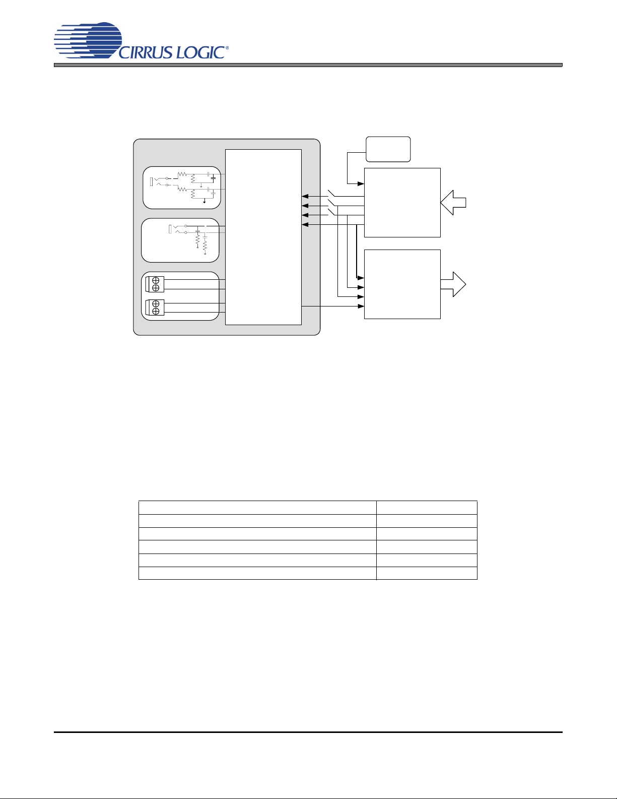
3. CONFIGURATION OPTIONS
This section provides a deeper understanding of on-board circuitry and digital clock and data signal routing for appropriately setting the control software in a spec ific configuration. The section also provides the expected performance characteristics for the respective configuration mode.
12.288 MHz
CRD42L52
R
T
Line
Input
Headphone
Output
Right
Left
R
T
CS42L52
(SLAVE)
AIN1A
AIN1B
HP/ LINE_OUTB
HP/ LINE_OUTA
SPKR_OUTB+
SPKR_OUTB-
SPKR_OUTA+
SPKR_OUTA-
Serial
Port
Enable
Oscillator
OMCK
SDOUT
LRCLK
SCLK
RMCK
MCLK
SCLK
LRCLK
SDIN
CS8416
S/PDIF Rx
(MASTER)
CS8406
S/PDIF Tx
(SLAVE)
S/PDIF
IN
S/PDIF
OUT
Figure 2. CRD42L52 and CDB42LDB1 Block Diagram for ADC and DAC Testing
In order to test the ADC, DAC and PWM on the CS42L52, S/PDIF di gital input needs to b e provided to the CS841 6
S/PDIF receiver on the CDB42LDB1 driver board via optical or RCA input jacks. The CS8416 operates in master
mode and drives the serial audio interface lines to the CS42L52 an d the CS8406, a s shown in Figure 2. For correct
CS42L52 serial port operation, the CS42L52 serial port should be set up as a slave and the “Driver Board Serial
Port” needs to be enabled in the FlexGUI software.
3.1 S/PDIF In to Headphone Out
Stereo headphone-level analog outputs can be moni tored on stereo jack J8 on th e CRD42L52. Serial Audio
digital clocks and data is routed to the CRD42L52 via I/O header J3. Table 1 shows expected performance
characteristics when the boards are configured to make digital input to analog output measurements.
Plot Location
FFT - S/PDIF In to Headphone Out @ 0 dBFS Figure 12 on page 15
FFT - S/PDIF In to Headphone Out @ -60 dB FS Figure 13 on page 16
Dynamic Range - S/PDIF In to Headphone Out Figure 14 on page 16
Frequency Response - S/PDIF In to Headphone Out Figure 15 on page 16
THD + N - S/PDIF In to Headphone Out Figure 16 on page 16
Ta bl e 1. S/PDIF In to Headphone Out Performance Plo ts
3.2 Line In to S/PDIF Out
Line-level analog input can be provided to the CS42L52 via stereo jack J7 on the CRD42L52. The analog
input path on the CRD42L52 scales the input down to a fifth of its actual value. Therefore, a 2.4 Vrms analog
input into the CRD42L52 is required to provide full-scale input to the CS42L52. The ADC core uses the
clocks provided to the CS42L52 by the CS8416 to perform the conversion and outputs data to the CS8406
S/PDIF transmitter on the CDB42LDB1 driver board via the I/O header, J3. The S/PDIF output can be monitored on the RCA or optical jacks (J9 and J7).
DS680RD1 7
Page 8
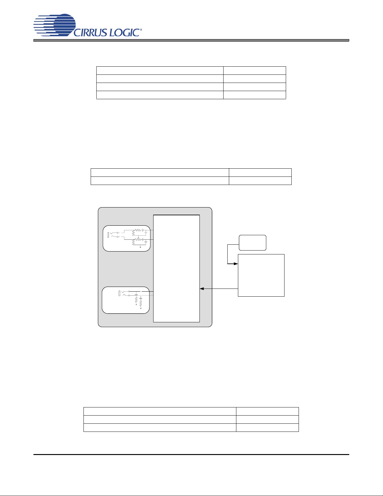
Table 2 shows expected performance characteristics when the boards are configured to make analog input
to digital output measurements.
Dynamic Range - Line In to S/PDIF Out Figure 9 on page 15
Frequency Response - Line In to S/PDIF Out Figure 10 on page 15
THD + N - Line In to S/PDIF Out Figure 11 on page 15
Table 2. Line In to S/PDIF Out Performance Plots
3.3 S/PDIF In to Speaker Out
Stereo differential speaker outputs from the CS42L52 can be monito red on screw terminals J3 and J4. The
CS42L52 can be set up to provide data to the PWM modulator for producing speaker outputs from either
the serial port PCM input or the ADC output using the FlexGUI softwar e. For a description of the Cirrus
FlexGUI software controls, refer to Section 4 on page 9. Table 3 shows expected performance characteris-
tics when the boards are configured to make speaker output measurements.
Frequency Response - S/PDIF In to Speaker Out Figure 17 on page 16
T able 3. S/PDIF In to Speaker Out Performance Plots
CRD42L52
Plot Location
Plot Location
CRD42L52
R
T
Line
Input
Headphone
Output
R
T
CS42L52
(MASTER)
AIN1A
AIN1B
HP/ LINE_OUTB
HP/ LINE_OUTA
Figure 3. CRD42L52 and CDB42LDB1 Block Diagram for Digital Loopback Testing
3.4 Analog In to Analog Out - Digital Loopback
In order to use the CS42L52 in digital loopback mode, one can configure the CS42L5 2 to operate in master
or slave mode. Figure 3 shows the board configuration when the CODEC is set up to operate in master
mode. In this mode, the CS42L52 receives an MCL K from the driver board fr om the CS8416 S/PDIF reciever. As described in Section 1.3 on page 4 and shown in Figure 3, the S/PDIF receiver us es the on-board
12.288 MHz clock as an MCLK when it is not receiving a S/PDIF input stream. Table 3 shows expected performance characteristics when the boards are configured to make speaker output measurements.
12.288 MHz
Oscillator
RMCK
SDOUT
LRCLK
SCLK
MCLK
(MASTER)
CS8416
S/PDIF Rx
Plot Location
Dynamic Range - Line In to HP Out (Digital Loopback) Figure 18 on page 16
THD + N - Line In to HP Out (Digital Loopback) Figure 19 on page 17
8 DS680RD1
Page 9
CRD42L52
4. SOFTWARE MODE CONTROL
The CRD42L52 may be used with the CDB42LDB1 driver board and the Microso ft® Windows-based FlexGUI graphical user interface, allowing sof tware contro l of the CS42 L52 and FPG A registe rs. The lates t control so ftware ma y
be downloaded from www.cirrus.com/msasoftware . Step-by-step instructions for setting up the FlexGUI are provided as follows:
1. Download and install the FlexGUI software as instructed on the Website.
2. Apply power using either an external source connected to screw terminal J1 or 3 AAA batteries (not included) on BT1, BT2 and BT3.
3. Connect the CDB42LDB1 to the host PC using a USB cable.
4. Launch the Cirrus FlexGUI. Once the GUI is launched successfully, all registers are set to their default reset
state.
5. Refresh the GUI by clicking on the Update button. The default state of all registers are now visible.
For standard set-up:
6. Set up the CS42L52 in the CODEC Configuration, Analog Input Volume Control, DSP Engine or Analog and
PWM Output Volume Controls tab as desired.
7. Begin evaluating the CS42L52.
For quick set-up, the CRD42L52 may, alternatively, be configured by loading a predefined sample script file:
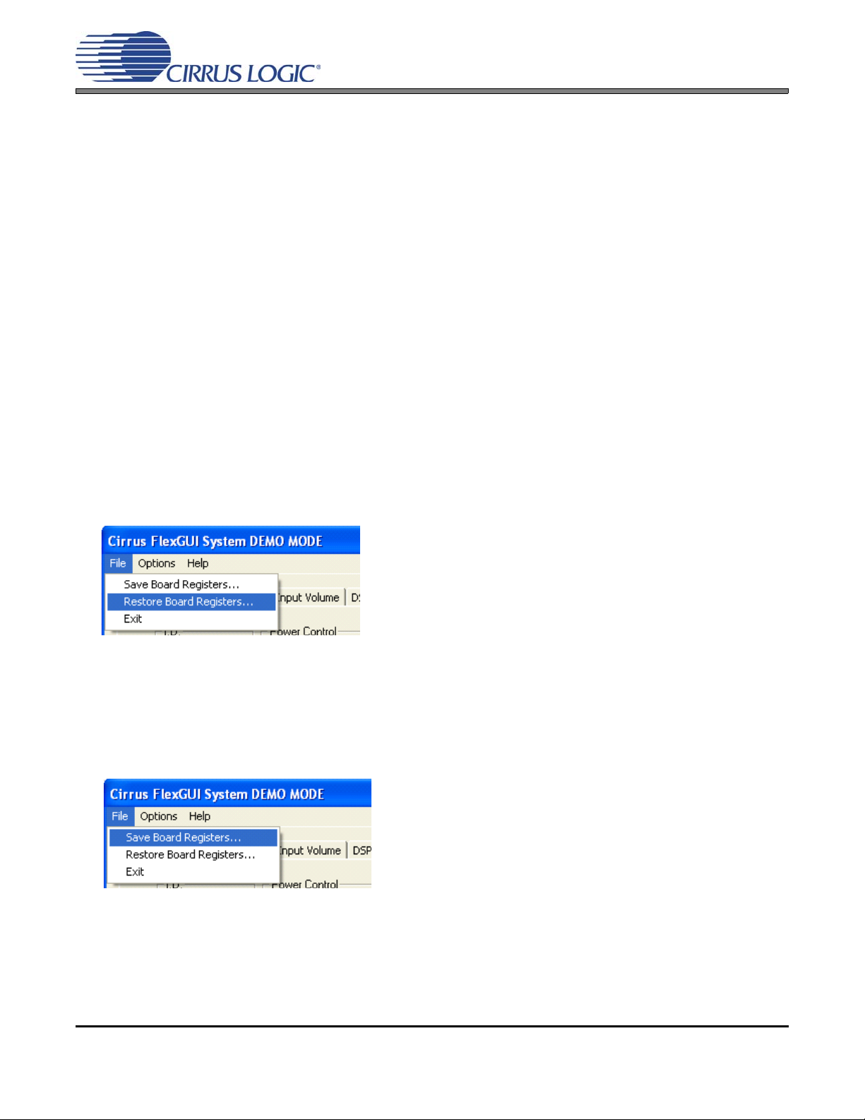
8. On the File menu, click Restore Board Registers...
9. Browse to Boards\CRD42L52\Scripts\.
10. Choose any one of the provided scripts to begin evaluation.
To create personal script files:
11. On the File menu, click Save Board Registers...
12. Enter any name that sufficiently describes the created setup.
13. Choose the desired location and save the script.
14. To load this script, follow the instructions from step 8 above.
DS680RD1 9
Page 10

4.1 CODEC Configuration Tab
The “CODEC Configuration” tab provides high-level control of various configurations for the CRD42L52.
Status text detailing the CODEC’s specific configuration appears directly below the associated control. This
text will change depending on the setting of the associated control. A description of each group is outlined
below. See the CS42L52 data sheet for complete register descriptions.
Power Control - Includes register controls for powering down the CODEC, ADC, PGA, headphone and
speaker amplifiers. Microphone pow er register controls are not included as they are not connected on the
CRD42L52 and are powered down by default.
ADC Input Configuration - Includes controls for the internal PGA MUX and analog inputs.
Serial Port Configuration - Includes controls for all settings related to the transmission and relationship of
data and clocks within the CODEC.
Driver Board Serial Port Disable - Controls the s witch that allows the CDB42LDB1 to drive the data/clock
I/O lines going to the CDB42LDB1 reference design board.
Update - Reads all registers in the CS42L52 and reflects the current values in the GUI.
CRD42L52
Figure 4. CODEC Configuration Tab
10 DS680RD1
Page 11

4.2 Analog Input Volume Tab
The “Analog Input Volume” tab provides high-level control of all volume settings in the ADC of th e CS42L52.
Status text detailing the CODEC’s specific configuration is shown inside the control group of the affected
control. This text will change depending on the setting of the associated control. A description of each group
is outlined below. See the CS42L52 data sheet for complete register descriptions.
Digital Volume Control - Includes digital volume controls and adjustments for the ADC.
ALC Configuration - Includes all configuration settings for the Automatic Level Control (ALC).
Analog Volume Control - Includes all analog volume controls and adjustments for the PGA.
Noise Gate Configuration - Includes all configuration settings for the noise gate.
Update - Reads all registers in the CS42L52 and reflects the current values in the GUI.
Reset - Resets the CS42L52.
CRD42L52
Figure 5. Analog Input Volume Tab
DS680RD1 11
Page 12

4.3 DSP Engine Tab
The “DSP Engine” tab provides high-level control of the SDIN (PCM) data volume level, the ADC output/SDIN mix volume level and the overall DAC/PWM channel volume level. DAC/PWM channel Limiter,
Tone Control and Beep Generator control functions are also provided.
Status text detailing the CODEC’s specific configuration is shown inside the control group of the affected
control. This text will change depending on the setting of the associated control. A description of each group
is outlined below. See the CS42L52 data sheet for complete register description s.
Digital Volume Control - Digital volume controls and adjustments for the SDIN data, ADC out data and overall channel volume. Mute, gang, invert and de-em ph a sis fun ct i on s are also ava ilab le .
Limiter - Configuration settings for the Automatic Level Control (ALC).
Tone Control - Bass and treble volume controls and filter corner frequencies.
Beep Generator - On/Off time, frequency, volume, mix and repeat beep functions.
Update - Reads all registers in the CS42L52 and reflects the current values in the GUI.
Reset - Resets the CS42L52.
CRD42L52
Figure 6. DSP Engine Tab
12 DS680RD1
Page 13

4.4 Analog and PWM Output Volume Tab
The “Analog and PWM Output Volume” tab provides high-level control of the CS42L52 input passthrough
volume, HP/Line output volume levels, charge pump frequency, speaker volume, and PWM Temperature/Battery monitoring controls. Status text detailing the CODEC’s specific configuration appears directly
below the associated control. This text will change depending on the setting of the associated control. A
description of each group is outlined below. See the CS42L52 data sheet for complete register descr iptions.
Headphone/Line Analog Output - Digital volume controls and adjustments for the DAC channel (outside of
the DSP) and for the input passthrough. The modulation index and gain settings make up the parameters
that determine the full scale headphone/line output level.
PWM Output - Volume, mute, power down and other functional controls for the PWM speaker outputs.
Temperature and Battery Monitor/Control - Battery Compensation, Thermal Foldback, Temperature Shut -
down and Battery Monitor for the PWM/Speaker outputs.
CRD42L52
Figure 7. Analog and PWM Output Volume Tab
DS680RD1 13
Page 14

4.5 Register Maps Tab
The Advanced Register Debug tab provides low-level control of the CS42L52 individual register settings.
Register values can be modified bit-wise or byte-wise. For bit-wise, click the appropriate push-b utton for the
desired bit. For byte-wise, the desired hex value can be typed directly into the register address box in the
register map. The “GPIO” tab may be ignored.
CRD42L52
Figure 8. Register Maps Tab
14 DS680RD1
Page 15

CRD42L52
50
+5
50
+0
5. PERFORMANCE PLOTS
Test conditions (unless otherwise specified): Input test signal is a full-scale 997 Hz sine wave; measurement bandwidth is 20 Hz to 20 kHz (unweighted); VA=VD=VA_HP=1.8 V; Sample Frequency = 48 kHz; HP test load:
R
L =10kΩ.
-
-52.5
-55
-57.5
-60
-62.5
-65
-67.5
-70
-72.5
d
B
-75
F
S
-77.5
-80
-82.5
-85
-87.5
-90
-92.5
-95
-97.5
-100
20 20k50 100 200 500 1k 2k 5k 10k
Hz
+4.5
+4
+3.5
+3
+2.5
+2
+1.5
+1
+0.5
d
B
-0
F
S
-0.5
-1
-1.5
-2
-2.5
-3
-3.5
-4
-4.5
-5
20 20k50 100 200 500 1k 2k 5k 10k
Hz
Figure 9. Dynamic Range - Line In to S/PDIF Out Figure 10. Freq. Resp. - Line In to S/PDIF Out
-
-52.5
-55
-57.5
-60
-62.5
-65
-67.5
-70
-72.5
d
B
-75
F
S
-77.5
-80
-82.5
-85
-87.5
-90
-92.5
-95
-97.5
-100
20 20k50 100 200 500 1k 2k 5k 10k
* (Note 1)
Hz
-10
-20
-30
-40
-50
-60
d
B
-70
r
A
-80
-90
-100
-110
-120
-130
-140
20 20k50 100 200 500 1k 2k 5k 10k
Hz
Figure 11. THD + N - Line In to S/PDIF Out Figure 12. FFT - S/PDIF In to HP Out @ 0 dBFS
Notes:
1. The total harmonic distortion + noise (THD+N) performance of the ADC in the CS42L52 is determined by
the value of the capacitor on the FILT+ pin. Larger ca pacitor values yield significant improvement in THD+N
at low frequencies. A 1 uF capacitor was used to make the performance measurement in Figure 12.
DS680RD1 15
Page 16

CRD42L52
+0
60
+3
60
+5
60
-
-10
-20
-30
-40
-50
-60
d
B
-70
r
A
-80
-90
-100
-110
-120
-130
-140
20 20k50 100 200 500 1k 2k 5k 10k
Hz
Figure 13. FFT - S/PDIF In to HP Out @ -60 dBFS Figure 14. Dynamic Range - S/PDIF In to HP Out
-62.5
-65
-67.5
-70
-72.5
-75
-77.5
-80
d
-82.5
B
-85
r
-87.5
A
-90
-92.5
-95
-97.5
-100
-102.5
-105
-107.5
-110
20 20k50 100 200 500 1k 2k 5k 10k
Hz
+2.75
+2.5
+2.25
+2
+1.75
+1.5
+1.25
+1
+0.75
+0.5
d
+0.25
B
+0
r
-0.25
A
-0.5
-0.75
-1
-1.25
-1.5
-1.75
-2
-2.25
-2.5
-2.75
-3
20 20k50 100 200 500 1k 2k 5k 10k
Hz
-
-62.5
-65
-67.5
-70
-72.5
-75
-77.5
-80
d
-82.5
B
-85
r
-87.5
A
-90
-92.5
-95
-97.5
-100
-102.5
-105
-107.5
-110
20 20k50 100 200 500 1k 2k 5k 10k
Hz
Figure 15. Freq. Resp. - S/PDIF In to HP Out Figure 16. THD + N - S/PDIF In to HP Out
-
+4.5
+4
+3.5
+3
+2.5
+2
+1.5
+1
d
+0.5
B
-0
r
-0.5
A
-1
-1.5
-2
-2.5
-3
-3.5
-4
-4.5
-5
20 20k50 100 200 500 1k 2k 5k 10k
Hz
-62
-64
-66
-68
-70
-72
-74
-76
d
-78
B
-80
r
-82
A
-84
-86
-88
-90
-92
-94
-96
-98
-100
20 20k50 100 200 500 1k 2k 5k 10k
Hz
Figure 17. Freq. Resp. - S/PDIF In to Spkr. Out Figure 18. Dynamic Range - Line In to HP Out (Dig. LB)
16 DS680RD1
Page 17

-
60
-62
-64
-66
-68
-70
-72
d
-74
B
r
-76
A
-78
-80
-82
-84
-86
-88
-90
20 20k50 100 200 500 1k 2k 5k 10k
*Note 1
Hz
Figure 19. THD + N - Line In to HP Out (Dig. LB)
CRD42L52
DS680RD1 17
Page 18

6. SYSTEM CONNECTIONS & INTERFACE
On CDB42LDB1:
CRD42L52
Connector/
Interface
AAA
Power Supply Switch S1 Input
External Power J1 Input +5 V - +2.7 V external power supply.
USB J2 Input/Output USB connection to PC for I²C control port signals.
S/PDIF OPTICAL OUT J7 Output CS8406 digital audio output via optical cable.
S/PDIF COAX OUT J9 Output CS8406 digital audio output via coaxial cable.
S/PDIF OPTICAL IN J6 Input CS8416 digital audio input via optical cable.
S/PDIF COAX IN J8 Input CS8416 digital audio input via coaxial cable.
MICRO JTAG J5 Input/Output I/O for programming the micro controller (U3).
MICRO RESET S4 Input Reset for the micro controller (U3).
I/O Header J3 Input/Output
Reference
Designator
BT1
BT2
BT3
Input/
Output Description
Input Battery Power Supply.
Switch that selects which power supply is used by the CDB42LDB1 and the
CRD42L52.
I/O routing between CDB42LDB1 and CRD42L52 containing Control Port
and Serial Audio Clock and Data .
On CRD42L52:
Connector/
Interface
Line Input J7 Input Stereo jack for line level input signal to analog input channel 1 on CS42L52.
Headphones J8 Output Stereo jack for monitoring stereo headphone output from CS42L52.
SPEAKER LEFT
SPEAKER RIGHT
I/O Header J5 Input/Output
Reference
Designator
J3
J4
Input/
Output Description
Output
Screw Terminals for monitoring differential stereo speaker output from
CS42L52.
I/O routing between CDB42LDB1 and CRD42L52 containing Control Port
and Serial Audio Clock and Data .
18 DS680RD1
Page 19

DS680RD1 19
CRD42L52 AND CDB42LDB1 BLOCK DIAGRAM
Speaker
Left
+
Right
+
-
CRD42L52
Line
-
Input
USB
Microcontroller
J3
J4
CS42L52
Headphone
Output
I²C
Control
J5
Port
SAI
Power
Supply
Micro Reset
Pushbutton
S/PDIF
Input
I²C Control Port
Interface
S/PDIF Rx
CS8416
MCLK
I/O Header
Serial Audio Interface
12.288 MHz
CRD
Placeholder
AAA Battery
Clip
S/PDIF Tx
CS8406
External
Power
S/PDIF
Output
CDB42LDB1
Figure 20. Block Diagram
CRD42L52
Page 20

20 DS680RD1
7. CRD42L52 SCHEMATICS
Figure 21. CS42L52 and Analog I/O
CRD42L52
Page 21

DS680RD1 21
8. CDB42LDB1 SCHEMATICS
Figure 22. S/PDIF Input/Output
CRD42L52
Page 22

22 DS680RD1
Figure 23. Microcontroller, Push Buttons and LED Indicators
CRD42L52
Page 23

9. CRD42L52 LAYOUT
CRD42L52
Figure 24. Silkscreen Top
Figure 25. Silkscreen Bottom
Figure 27. Internal Layer (Ground Plane)
Figure 28. Internal Layer (Power Plane)
Figure 26. Top-Side Layer
DS680RD1 23
Figure 29. Bottom-Side Layer
Page 24

10.CDB42LDB1 LAYOUT
CRD42L52
Figure 30. Silkscreen Top
Figure 31. Silkscreen Bottom
24 DS680RD1
Page 25

CRD42L52
Figure 32. Top-Side Layer
Figure 33. Layer 2
DS680RD1 25
Page 26

CRD42L52
Figure 34. Layer 3
Figure 35. Bottom-Side Layer
26 DS680RD1
Page 27

11.REVISION HISTORY
Release Changes
RD1 Initial Release
CRD42L52
DS680RD1 27
Page 28

CRD42L52
Contacting Cirrus Logic Support
For all product questions and inquiries, contact a Cirrus Logic Sales Representative.
To find the one nearest you, go to www.cirrus.com.
IMPORTANT NOTICE
Cirrus Logic, Inc. and its subsidiaries (“Cirrus”) believe that the information contained in this document is accurate and reliable. However, the information is subject
to change without noti ce and is p rovided “AS IS” wit hout warran ty of any k ind (expr ess or i mplied). Customers are advis ed to ob tain the latest version of relevant
information to verify, before placing orders, that information being relied on is current and complete. All products are sold subject to the terms and conditions o f sale
supplied at the time of order acknowledgment, including those pertaining to warranty, indemnification, and limitation of liability. No responsibility is assumed by Cirrus
for the use of this information, including use of this information as the basis for manufacture or sale of any items, or for infringement of patents or other rights of third
parties. This document is the property of Cirrus and by furnishing this information, Cirrus grants no license, express or implied under any patents, mask work rights,
copyrights, trademarks, trade secrets or other inte llectual property rig hts. Cirrus owns the copyrights associated with the information contained herein and gives consent for copies to be made of the information only for use within your organization with respect to Cirrus integrated circuits or other products of Cirrus. This consent
does not extend to other copying such as copying for general distribution, advertising or promotional purposes, or for creating any work for resale.
CERTAIN APPLICATIONS USING SEMICONDUCTOR PRODUCTS MAY INVOLVE POTENTIAL RISKS OF DEATH, PERSONAL INJURY, OR SEVERE PROPERTY OR ENVIRONMENTAL DAMAGE (“CRITICAL APPLICATIONS”). CIRRUS PRODUCTS ARE NOT DESIGNED, AUTHORIZED OR WARR ANTED FOR USE
IN PRODUCTS SURGICALLY IMPLANTED INTO THE BODY, AUTOMOTIVE SAFETY OR SECURITY DEVICES, LIFE SUPPORT PRODUCTS OR OTHER CRITICAL APPLICATIONS. INCLUSION OF CIRRUS PRODUCTS IN SUCH APPLICATIONS IS UNDERSTOOD TO BE FULLY AT THE CUSTOM ER’S RISK AND CIRRUS DISCLAIMS AND MAKES NO WARRANTY, EXPRESS, STATUTORY OR IMPLIED, INCLUDING THE IMPLIED WARRANTIES OF M ERCHANTABILITY AND
FITNESS FOR PARTICULAR PURPOSE, WITH REGARD TO ANY CIRRUS PRODUCT THAT IS USED IN SUCH A MANNER. IF THE CUSTOMER OR CUSTOMER’S CUSTOMER USES OR PERMITS THE USE OF CIRRUS PRODUCTS IN CRITICAL APPLICATIONS, CUSTOMER AGREES, BY SUCH USE, TO FULLY
INDEMNIFY CIRRUS, ITS OFFICERS, DIRECTORS, EMPLOYEES, DISTRIBUTORS AND OT HER AGE NTS FRO M ANY AND AL L LI ABI L IT Y, I NCL UDING ATTORNEYS’ FEES AND COSTS, THAT MAY RESULT FROM OR ARISE IN CONNECTION WITH THESE USES.
Cirrus Logic, Cirrus, and the Cirrus Logic logo design s ar e tra de m a rks of Ci rru s Lo gi c, Inc. All o ther bra nd and product names in this document may be trademarks
or service marks of their respective owners.
I²C is a registered trademark of Philips Semiconductor.
Microsoft and Windows are registered trademarks of Microsoft Corporation.
28 DS680RD1
 Loading...