

Page 1
Shutdown
Control (J2)
Speaker
Outpu t ( J 3)
Optional
Gain
Adjustment
Analog
Inpu t ( J 1 )
CS35L01
(SD Mode)
Optional
Output
Filter
VBATT
Power (J4 )
Shutdown
Control (J2)
Speaker
Outpu t ( J 3)
Optional
Gain
Adjustment
Analog
Inpu t ( J 1 )
CS35L01
(FSD Mode)
Optional
Output
Filter
VBATT
Power (J4)
Shutdown
Control (J2)
Speaker
Outpu t ( J 3)
Optional
Gain
Adjustment
Analog
Inpu t ( J 1 )
CS35L01
(HD M ode)
Optional
Output
Filter
VBATT
Power (J4)
Shutdown
Control (J2)
Speaker
Outpu t ( J 3)
Optional
Gain
Adjustment
Analog
Inpu t ( J 1 )
CS35L01
(FHD Mod e)
Optional
Output
Filter
VBATT
Power (J4)
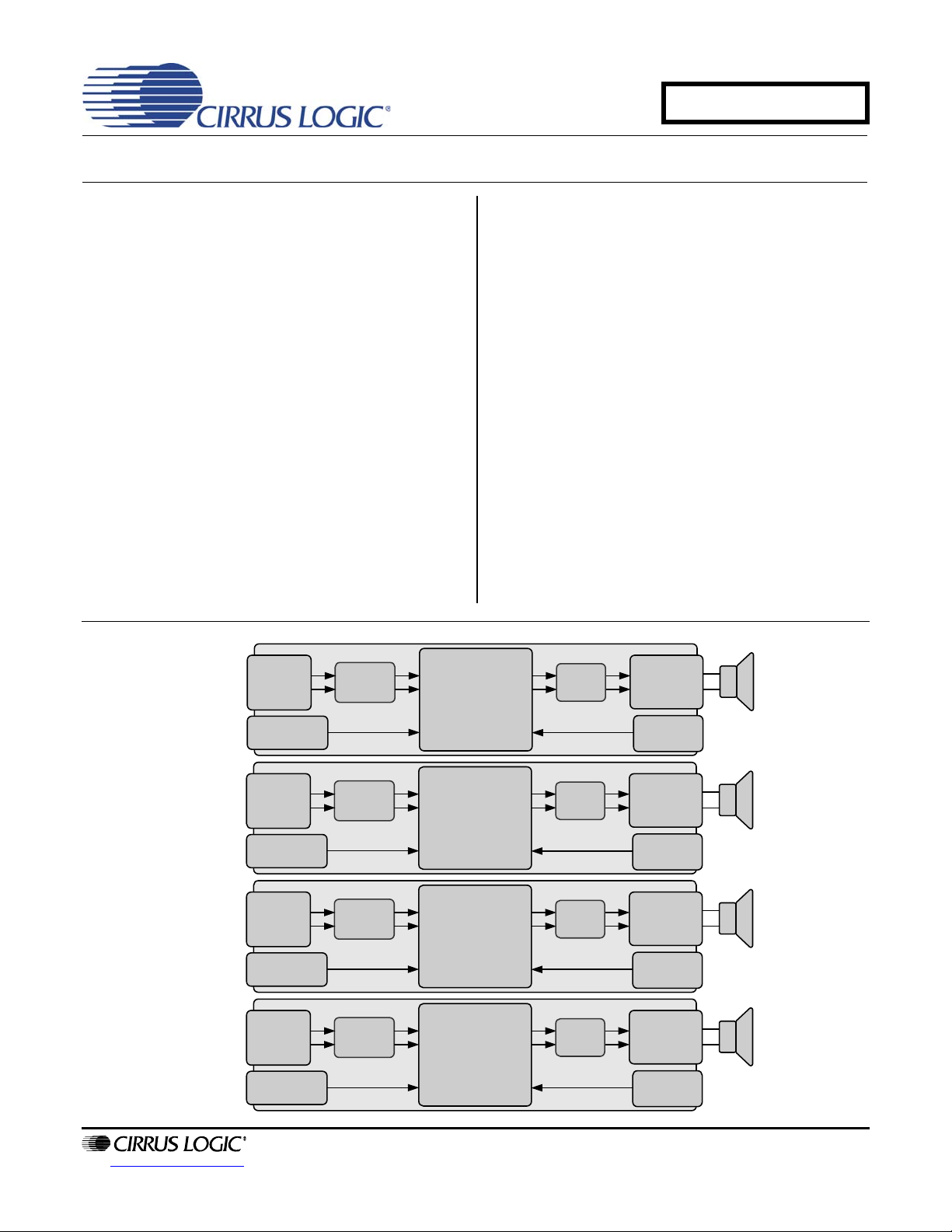
CRD35L01
1 x 1.7 W CS35L01 Amplifier Reference Design Kit
Features
Four boards provided in the CS35L01 Amplifier
Reference Design Kit
Separate boards for each mode configuration
– SD, FSD, HD, and FHD
CS35L01 produces a default +6-dB Gain
Delivers 1.4 W/Ch into 8 at 1% THD+N
Delivers 1.7 W/Ch into 8 at 10% THD+N
Differential mono analog inputs
Demonstrates recommended 4-layer layout
and grounding arrangements
– Optional output filter connections
– Optional gain adjustment resistors
Powered by a single 2.5- to 5.5-V power supply
Device shutdown control
Description
The CRD35L01 demonstrates the CS35L01 high-efficiency Hybrid Class-D audio amplifier. This reference
design implements a single-channel amplifier that delivers 1.7 W per full-bridge channel into 8- loads using a
single +5-V supply.
Differential audio inputs can easily be connected
through the J1 header. If desired, the gain can be adjusted through the optional input resistors.
The -SD, -FSD, -HD, or -FHD suffix designates the
CS35L01’s operational mode. Each of the four boards
is configured to operate in each of the four corresponding modes of the CS35L01 device.
Device shutdown control is available through the J2
header.
ORDERING INFORMATION
CRD35L01 CS35L01 Reference Design
http://www.cirrus.com
Copyright Cirrus Logic, Inc. 2010
(All Rights Reserved)
APR '10
DS914RD2
Page 2

TABLE OF CONTENTS
1. SYSTEM OVERVIEW ............................................................................................................................. 4
1.1 CS35L01 Hybrid Class-D Amplifier .................................................................................................. 4
1.2 Power Supply ................................................................................................................................... 4
1.3 Operational Modes ........................................................................................................................... 4
1.4 Shutdown Control ............................................................................................................................ 4
1.5 Amplifier Gain .................................................................................................................................. 4
1.5.1 Optional Input Gain Adjustment Resistors ...................................................... ... ... .... ... ... ........ 4
1.6 Differential Analog Inputs ................................................................................................................. 5
1.7 Speaker Outputs .............................................................................................................................. 5
1.7.1 Optional Speaker Output EMI Filter Components ........... ........................................................ 5
2. GROUNDING AND POWER SUPPLY DECOUPLING .......................................................................... 6
2.1 Power Supply Decoupling ................................................................................................................ 6
2.2 Electromagnetic Interference (EMI) ................................................................................................. 6
2.2.1 Suppression of EMI at the Source ......................... ... .... ... ... ... ... ....................................... ... ..... 6
3. SYSTEM CONNECTORS AND JUMPERS ....... ... ... ... .... ...................................... .... ... ... ... ... .... ... ... ... .... . 7
4. CRD SCHEMATIC .................................................................................................................................. 8
4.1 Bill of Materials ................................................................................................................................. 9
5. CRD LAYOUT ....................................................................................................................................... 10
6. REVISION HISTORY ............................................................................................................................ 14
CRD35L01
LIST OF FIGURES
Figure 1.Optional Bypass Trace Cut Locations ........................................................................................... 5
Figure 2.CRD35L01-SD Schematic ................... .... ... ... ... .... ... ... ... .... ... ... ... ... .... ... ... ..................................... 8
Figure 3.CRD35L01-FSD Schematic .................................................. .......................................... ... ........... 8
Figure 4.CRD35L01-HD Schematic .................................................... ... ... ... .... ... ... ... .... ... ... ........................ 8
Figure 5.CRD35L01-FHD Schematic .................................. ... ... ... .... ... ... ... ... .... ........................................... 8
Figure 6.CRD35L01-SD Top Side Component Placement . ... ... ... .... ... ... ... ... .... ... ... ... .... ... ... ... ... .... ... ... ... ... 10
Figure 7.CRD35L01-SD Bottom Side Component Placement .................. ............................................. ... 10
Figure 8.CRD35L01-SD Layer 1 Copper ........................ .... ... ... ... .... ... ... .......................................... ... ...... 10
Figure 9.CRD35L01-SD Layer 2 Copper ........................ .... ... ... ... .... ... ... .......................................... ... ...... 10
Figure 10.CRD35L01-SD Layer 3 Copper ................................................................................................ 10
Figure 11.CRD35L01-SD Layer 4 Copper ................................................................................................ 10
Figure 12.CRD35L01-FSD Top Side Component Placement ................................................................... 11
Figure 13.CRD35L01-FSD Bottom Side Component Placement ........................ ... ... .... ... ... ... ... .... ... ... ... ... 11
Figure 14.CRD35L01-FSD Layer 1 Copper .............................................................................................. 11
Figure 15.CRD35L01-FSD Layer 2 Copper .............................................................................................. 11
Figure 16.CRD35L01-FSD Layer 3 Copper .............................................................................................. 11
Figure 17.CRD35L01-FSD Layer 4 Copper .............................................................................................. 11
Figure 18.CRD35L01-HD Top Side Component Placement ............................ ... ... ... .... ... ... ... ................... 12
Figure 19.CRD35L01-HD Bottom Side Component Placement ............. ................ ................... ................ 12
Figure 20.CRD35L01-HD Layer 1 Copper ................................................................................................ 12
Figure 21.CRD35L01-HD Layer 2 Copper ................................................................................................ 12
Figure 22.CRD35L01-HD Layer 3 Copper ................................................................................................ 12
Figure 23.CRD35L01-HD Layer 4 Copper ................................................................................................ 12
Figure 24.CRD35L01-FHD Top Side Component Placement .......................... ................ ................ ......... 13
Figure 25.CRD35L01-FHD Bottom Side Component Placement ............................................................. 13
Figure 26.CRD35L01-FHD Layer 1 Copper .............................................................................................. 13
Figure 27.CRD35L01-FHD Layer 2 Copper .............................................................................................. 13
Figure 28.CRD35L01-FHD Layer 3 Copper .............................................................................................. 13
Figure 29.CRD35L01-FHD Layer 4 Copper .............................................................................................. 13
2 DS914RD2
Page 3

LIST OF TABLES
Table 1. System Input and Output Connections ......................................................................................... 7
Table 2. J2 Shutdown Control Settings ....................................................................................................... 7
Table 3. Bill of Materials Listing .................................................................................................................. 9
CRD35L01
DS914RD2 3
Page 4

CRD35L01
1. SYSTEM OVERVIEW
The CRD35L01 reference design is a practical means for eva luating the CS35L01 high-efficiency Class-D audio amplifier with idle current consumption. A differential mono analog input signal interface is provided. Option al input gain
and output filtering component placeholders are provided for easy modificatio n to custom tune the CS3 5L01 for the
user’s specific system requirements.
1.1 CS35L01 Hybrid Class-D Amplifier
The CS35L01 Hybrid Class-D amplifier is a mono, full-bridge, closed-loop, +6-dB gain, audio amplifier available in a 9-ball, WLCSP package. A complete description of the CS35 L01 device is included in the CS35L01
product data sheet.
1.2 Power Supply
A single +2.5 to +5.5 VDC power supply is required to power the CRD35L01. The supply must be capable
of delivering sufficient current for the intended power output. The supply provides power to the CS35L01.
The power supply connection to the board is provided by the header J4. The positive terminal is labeled
VBATT. The ground terminal is labeled GND.
1.3 Operational Modes
The CS35L01 device has four operational modes, each of which r equire slightly differ ent hardware connections. Four boards are available to illustrate the hardware design differences between each of the four
modes. More information on the specifics of each operational mode can be found in the CS35L01/03 pro duct datasheet. The CRD names listed below are populated with a CS35L01 device.
• CRD35L01-SD: Standard Class-D Mode
• CRD35L01-FSD: Reduced-Frequency Standard Class-D Mode
• CRD35L01-HD: Hybrid Class-D Mode
• CRD35L01-FHD: Reduced-Frequency Hybrid Class-D Mode
The CRD35L01-SD schematic is shown in Figure 2 on page 8. The CRD35L01-FSD schematic is shown in
Figure 3 on page 8. The CRD35L01-HD schematic is shown in Figure 5 on page 8. The CRD35L01-FHD
schematic is shown in Figure 5 on page 8.
1.4 Shutdown Control
The J2 header contains shutdown control for the CS35L01 device. Placing a jumper across the J2 header
pulls the SD
by the R3 resistor, enabling normal operation.
line LOW and shuts down the amplifier. When no jumper is present, the SD line is pulled HIGH
1.5 Amplifier Gain
The amplifier gain of the CS35L01 device is +6 dB by default. The amplifier gain can be reduced through
the use of the optional input gain adjustment resistors on the CRD35L01.
1.5.1 Optional Input Gain Adjustment Resistors
The CRD35L01 contains optional gain adjustment resistor placeholders (R1 and R2). By default, these
placeholders are not populated and are bypassed with a signal trace configuring the CS35 L01 to operate
at its default gain. The gain adjustment resistors are necessary only when a gain of +6 dB is not desired.
4 DS914RD2
Page 5
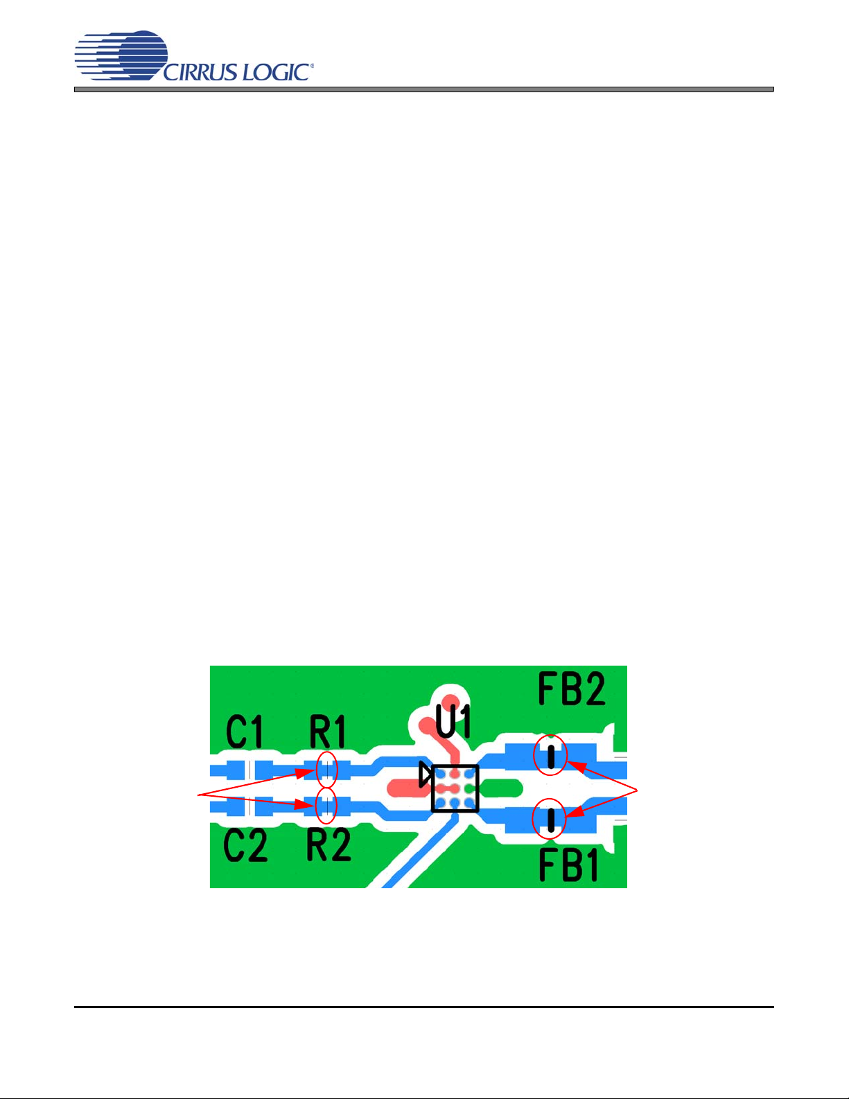
By adding series resistance to the input, the signal amplitude to the CS35L01 will be reduced, and will
Figure 1. Optional Bypass Trace Cut Locations
Cut the bypass
traces before inserting the optional
input gain adjustment resistors
Cut the bypass
traces before inserting the optional output filter ferrite
beads
reduce the overall system gain. The typical input impedance values of the CS35L01 can be found in the
device datasheet.
In order to use the optional gain adjustment resistors, the traces between the R1 pads and the traces between the R2 pads must be cut to break the bypass circuit, before populatin g R1 and R2 with the desired
resistance values. The location of these required cuts are sho wn in F i gure 1 . After th e trace be twe en th e
pads has been broken, the gain adjustment resistors can be added to the board.
1.6 Differential Analog Inputs
The differential audio inputs into the CS35L01 are provided by the 3-pin header (J1) through DC blocking
capacitors (C1 and C2). The C1 and C2 capacitors allow for an analog source to connect directly to the
CS35L01 regardless of any DC bias that may be present between the analog audio source’s outputs and
CS35L01 inputs.
1.7 Speaker Outputs
The CS35L01 power outputs are configured for a full-bridge, single audio channel. The outputs are routed
through an optional EMI output filter and then presented at the J3 header (OUT- and OUT+).
1.7.1 Optional Speaker Output EMI Filter Components
CRD35L01
As mentioned above, the CS35L01 contains optional placeholders for a series ferrite bead and shunt capacitor output filter. For most applications with very short speaker leads between the CS35L01 and the
speaker, use of these components will not be necessary. However, if there is a long signal path between
the CS35L01 and the speaker or if the system requires connecting to cables off the PCB, it is suggested
that the ferrite bead and capacitor are populated with the recommended values shown in Figure 3 on
page 9.
In order to use the optional output filter ferrite beads, the traces between the L1 pads and the traces between the L2 pads must be cut to break the bypass circuit, before populating L1 and L2 with the desired
component values. The location of these required cuts are shown in Figure 1.
DS914RD2 5
Page 6

CRD35L01
2. GROUNDING AND POWER SUPPLY DECOUPLING
The CS35L01 requires careful attention to power supply and grounding arrangements to optimize p erformance and
minimize radiated emissions. The decoupling capacitors should be located as close to the CS35L01 as possible.
This can be optimized by using both top and bottom side component p opulation as demonstrated by the CRD35L01
boards.
2.1 Power Supply Decoupling
Proper power supply decoupling is one key to maximizing the per formance of a Class-D amp lifier. Figure 6
and Figure 7 on page 10 show the compon en t place ment for the CRD35 L0 1-SD board . Figure 18 and Fig-
ure 19 on page 12 shows the component side placement for the CRD35L01-HD board. Note the addition of
the C8 capacitor connected to the LFILT+ pin. This pin is used as de coupling for th e internal LDO re gulator
when operating in HD or FHD modes.
The small value decoupling capacitors are placed as close as possible to the power pins of the CS35L01
on the CRD35L01 boards. For the WLCSP package it is recommended that the power supply decoupling
capacitors reside on the opposite si de of the board from which the CS35L01 is populated on. This allows
for very close placement of the decoupling capacitors to the power supply pins of the CS35L01 without interfering with the differential audio inputs or differential audio outputs. This placement keeps the high-frequency current loop small to minimize power supply variations and EMI. These capacitor s ar e no t r equir ed
to be expensive low-ESR capacitors.
2.2 Electromagnetic Interference (EMI)
This reference design is a board-level solution that is meant to control emissions by minimizing and suppressing them at the source, in contrast to containing them in an enclosure.
2.2.1 Suppression of EMI at the Source
Several techniques are used in the circuit design and board layout to minimize high-frequency fields in
the immediate vicinity of the high-power components. Specific techniques include the following:
• As mentioned in Section 2.1, effective power supply decoupling of high-frequency currents and minimizing the loop area of the decoupling loop is one aspect of minimizing EMI.
• Differential input and output signals should be routed differentially whenever possible.
• A solid ground plane on the adjacent PCB layer underneath all high-frequency traces to minimize the
loop area of the return path.
• Optional output EMI filter component landings are available as described in Section 1.7.1, if emissions
need to be further reduced.
• Keeping the switching output filter components as close to the amplifier as possible.
6 DS914RD2
Page 7
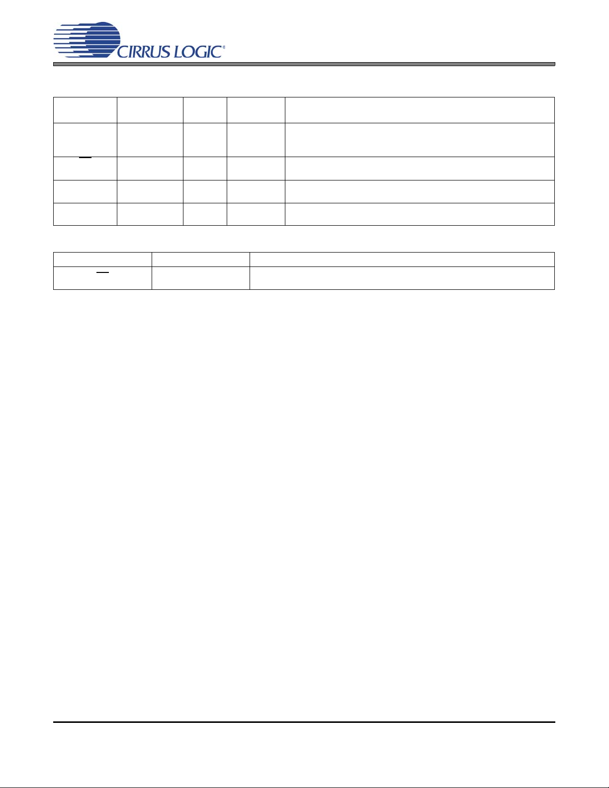
3. SYSTEM CONNECTORS AND JUMPERS
CRD35L01
Connector
Name
IN+
IN-
GND
SD
GND
OUT+
OUT-
VBATT
GND
Reference
Designator
J1
J1
J1
J2
J2
J3
J3
J4
J4
Pin Signal
Connector Function
Direction
1
2
3
1
2
1
2
1
2
Table 1. System Input and Output Connections
Input
Input
GND
Input
GND
Output
Output
Input
Input
Differential analog input (+) to CS35L01.
Differential analog input (-) to CS35L01.
GND reference connection.
Device shutdown control.
GND reference connection.
Analog output (+) from CS35L01.
Analog output (-) from CS35L01.
Positive connection from power supply, +2.5 to +5.5 VDC.
GND connection from power supply.
Control Name Function Function Selected
SD Shutdown
Low = CS35L01 shutdown enabled
High = CS35L01 shutdown disabled
Table 2. J2 Shutdown Control Settings
DS914RD2 7
Page 8

4. CRD SCHEMATIC
Figure 3. CRD35L01-FSD Schematic
Figure 2. CRD35L01-SD Schematic
Figure 4. CRD35L01-HD Schematic Figure 5. CRD35L01-FHD Schematic
CRD35L01
8 DS914RD2
Page 9

CRD35L01
4.1 Bill of Materials
The component listing below is shown for the four CRD35L01 board variations (-SD, -FSD, -HD, and -FHD).
Unpopulated (DNP) components are listed with recommended components for reference purposes.
Reference
Qty
(DNP) C4, C5 -SD, -FSD, -HD, -FHD Capacitor, 1 nF, X7R, 50 V Murata / GRM155R71H102KA01D
(DNP) FB1, FB2 -SD, -FSD, -HD, -FHD Ferrite Bead, 220
(DNP) R1, R2 -SD, -FSD, -HD, -FHD Resistor, 0
Designator(s) CRD35L01 Boards Description MFG / Part Number
2 C1, C2 -SD, -FSD, -HD, -FHD Capacitor, 0.1 F, X7R, 16 V Kemet / C0402C104K4RAC
1 C3 -SD, -FSD, -HD, -FHD Capacitor, 1 F, X5R, 10V Kemet / C0603C105K8PAC
1 C6 -SD, -FSD, -HD, -FHD Capacitor, 10 F, X5R, 6.3 V Kemet / C0603C106M9PAC
1 C7 -SD, -FSD, -HD, -FHD Capacitor, 0.1 F, X7R, 16 V Kemet / C0402C104K4RAC
1 C8 -HD, -FHD (Note 1) Capacitor, 1 F, X5R, 10 V Kemet / C0603C105K8PAC
1 R3 -SD, -FSD, -HD, -FHD Resistor 47k
1 U1 -SD, -FSD, -HD, -FHD Hybrid Class-D WLCSP Amp Cirrus Logic / CS35L01-CWZ
, 1/16 W Dale / CRCW040247K0JNED
@ 100 MHz TDK / MPZ1608S221A
, 1/16 W Yageo / RC0402JR-070RL
Table 3. Bill of Materials Listing
Note:
1. C8 is not present on SD or FSD boards. LFILT+ (B1) is connected directly to VBATT.
DS914RD2 9
Page 10

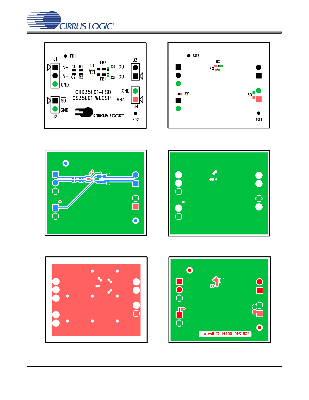
5. CRD LAYOUT
Figure 6. CRD35L01-SD Top Side Component
Placement
Figure 7. CRD35L01-SD Bottom Side Component
Placement
Figure 8. CRD35L01-SD Layer 1 Copper
Figure 9. CRD35L01-SD Layer 2 Copper
Figure 10. CRD35L01-SD Layer 3 Copper
Figure 11. CRD35L01-SD Layer 4 Copper
CRD35L01
10 DS914RD2
Page 11
CRD35L01
Figure 12. CRD35L01-FSD Top Side Component
Placement
Figure 13. CRD35L01-FSD Bottom Side Component
Placement
Figure 15. CRD35L01-FSD Layer 2 Copper
Figure 14. CRD35L01-FSD Layer 1 Copper
Figure 16. CRD35L01-FSD Layer 3 Copper
Figure 17. CRD35L01-FSD Layer 4 Copper
DS914RD2 11
Page 12

CRD35L01
Figure 18. CRD35L01-HD Top Side Component
Placement
Figure 19. CRD35L01-HD Bottom Side Component
Placement
Figure 20. CRD35L01-HD Layer 1 Copper
Figure 21. CRD35L01-HD Layer 2 Copper
Figure 22. CRD35L01-HD Layer 3 Copper
Figure 23. CRD35L01-HD Layer 4 Copper
12 DS914RD2
Page 13

CRD35L01
Figure 24. CRD35L01-FHD Top Side Component
Placement
Figure 29. CRD35L01-FHD Layer 4 Copper
Figure 25. CRD35L01-FHD Bottom Side Compo-
nent Placement
Figure 26. CRD35L01-FHD Layer 1 Copper
Figure 27. CRD35L01-FHD Layer 2 Copper
Figure 28. CRD35L01-FHD Layer 3 Copper
DS914RD2 13
Page 14

6. REVISION HISTORY
Contacting Cirrus Logic Support
For all product questions and inquiries, contact a Cirrus Logic Sales Representative.
To find the one nearest to you, go to www.cirrus.com.
IMPORTANT NOTICE
Cirrus Logic, Inc. and its subsidiaries (“Cirrus”) believe that the information contai ned in this document is accurate and reliable. However, the information is subject
to change without noti ce and is p rovided “AS IS” wit hout warran ty of any k ind (expr ess or i mplied). Customers are advis ed to ob tain the latest version of relevant
information to verify, before placing orders, that information being relied on is current and complete. All products are sold subject to the terms and conditions of sale
supplied at the time of order acknowledgment, including those pertaining to warranty, indemnification, and limitation of liability. No responsibility is assumed by Cirrus
for the use of this information, including use of this information as the basis for manufacture or sale of any items, or for infringement of patents or other rights of third
parties. This document is the property of Cirrus and by furnishing this information, Cirrus grants no license, express or implied under any patents, mask work rights,
copyrights, trademarks, trade secrets or other inte llectual property rig hts. Cirrus owns the copyrights associated with the information contained herein and gives consent for copies to be made of the information only for use within your organization with respect to Cirrus integrated circuits or other products of Cirrus. This consent
does not extend to other copying such as copying for general distribution, advertising or promotional purposes, or for creating any work for resale.
CERTAIN APPLICATIONS USING SEMICONDUCTOR PRODUCTS MAY INVOLVE POTENTIAL RISKS OF DEATH, PERSONAL INJURY, OR SEVERE PROPERTY OR ENVIRONMENTAL DAMAGE (“CRITICAL APPLICATIONS”). CIRRUS PRODUCTS ARE NOT DESIGNED, AUTHORIZED OR WARR ANTED FOR USE
IN PRODUCTS SURGICALLY IMPLANTED INTO THE BODY, AUTOMOTIVE SAFETY OR SECURITY DEVICES, LIFE SUPPORT PRODUCTS OR OTHER CRITICAL APPLICATIONS. INCLUSION OF CIRRUS PRODUCTS IN SUCH APPLICATIONS IS UNDERSTOOD TO BE FULLY AT THE CUSTOM ER’S RISK AND CIRRUS DISCLAIMS AND MAKES NO WARRANTY, EXPRESS, STATUTORY OR IMPLIED, INCLUDING THE IMPLIED WARRANTIES OF MER CHANTABILITY AND
FITNESS FOR PARTICULAR PURPOSE, WITH REGARD TO ANY CIRRUS PRODUCT THAT IS USED IN SUCH A MANNER. IF THE CUSTOMER OR CUSTOMER’S CUSTOMER USES OR PERMITS THE USE OF CIRRUS PRODUCTS IN CRITICAL APPLICATIONS, CUSTOMER AGREES, BY SUCH USE, TO FULLY
INDEMNIFY CIRRUS, ITS OFFICERS, DIRECTORS, EMPLOYEES, DISTRIBUTORS AND OT HER AGE NTS FRO M ANY AND AL L LI ABI L IT Y, I NCL UDING ATTORNEYS’ FEES AND COSTS, THAT MAY RESULT FROM OR ARISE IN CONNECTION WITH THESE USES.
Cirrus Logic, Cirrus, and the Cirrus Logic logo design s ar e tra de m a rks of Ci rru s Lo gi c, Inc. All o ther bra nd and product names in this document may be trademarks
or service marks of their respective owners.
Release Changes
RD1 – Initial Release
RD2 – Updated front page 1% and 10% output power numbers to match DS909A2 datasheet.
– Updated Figure 2 on page 8 to match the updated CRD35L01-SD Rev A1 schematic.
– Updated Figure 3 on page 8 to match the updated CRD35L01-FSD Rev A1 schematic.
– Updated Figure 4 on page 8 to match the updated CRD35L01-HD Rev A1 schematic.
– Updated Figure 5 on page 8 to match the updated CRD35L01-FHD Rev A1 schematic.
– Updated BOM values for C6 & C7 in Table 3 on page 9 to match the updated Rev A1 schematics and
the typical connection diagram in the DS909A2 datasheet. All CRD35L01-SD, -FSD, -HD, and -FHD
boards with an assembly date of 02/15/10 or earlier contain components from the Rev A0 BOM.
CRD35L01
14 DS914RD2
 Loading...