

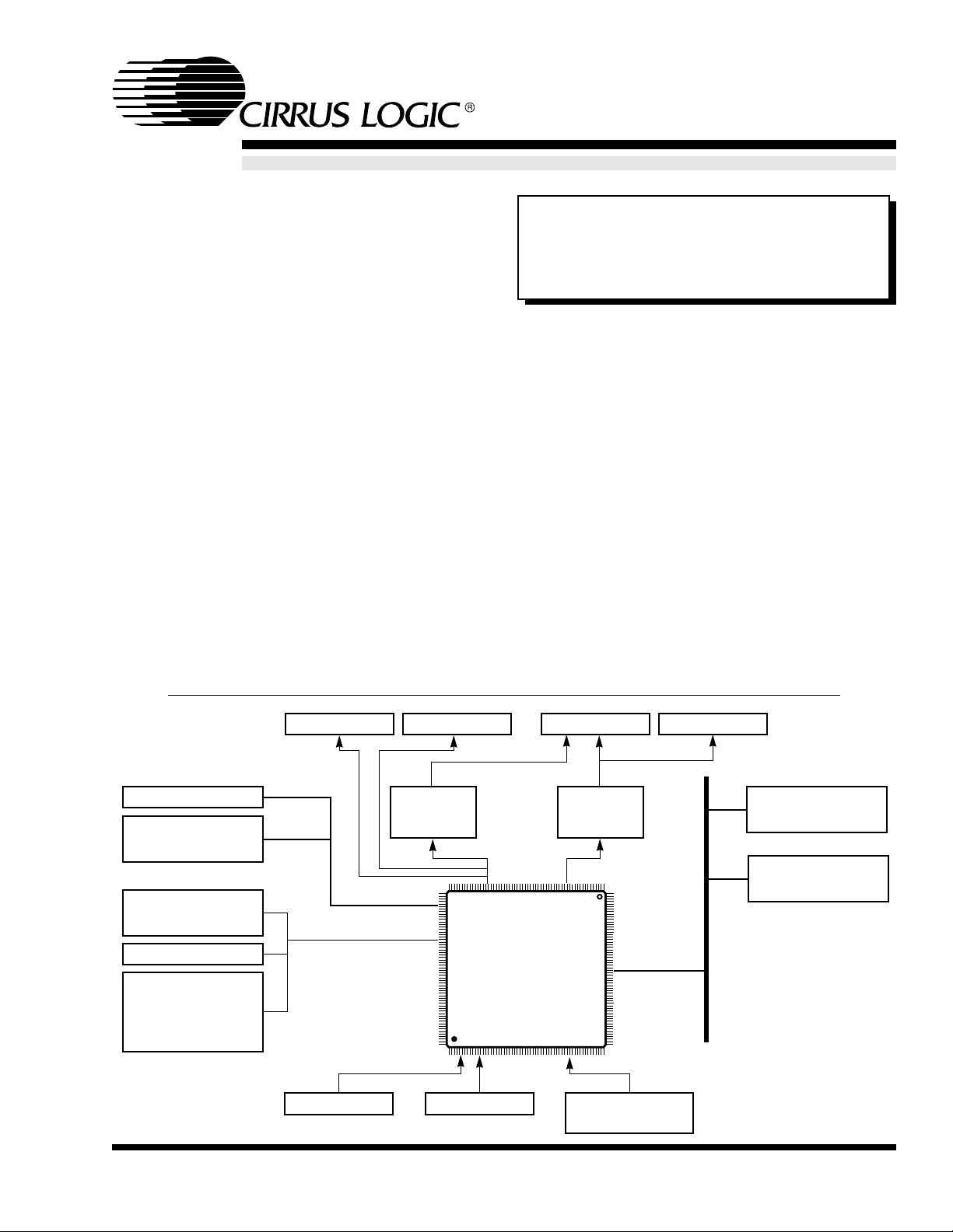
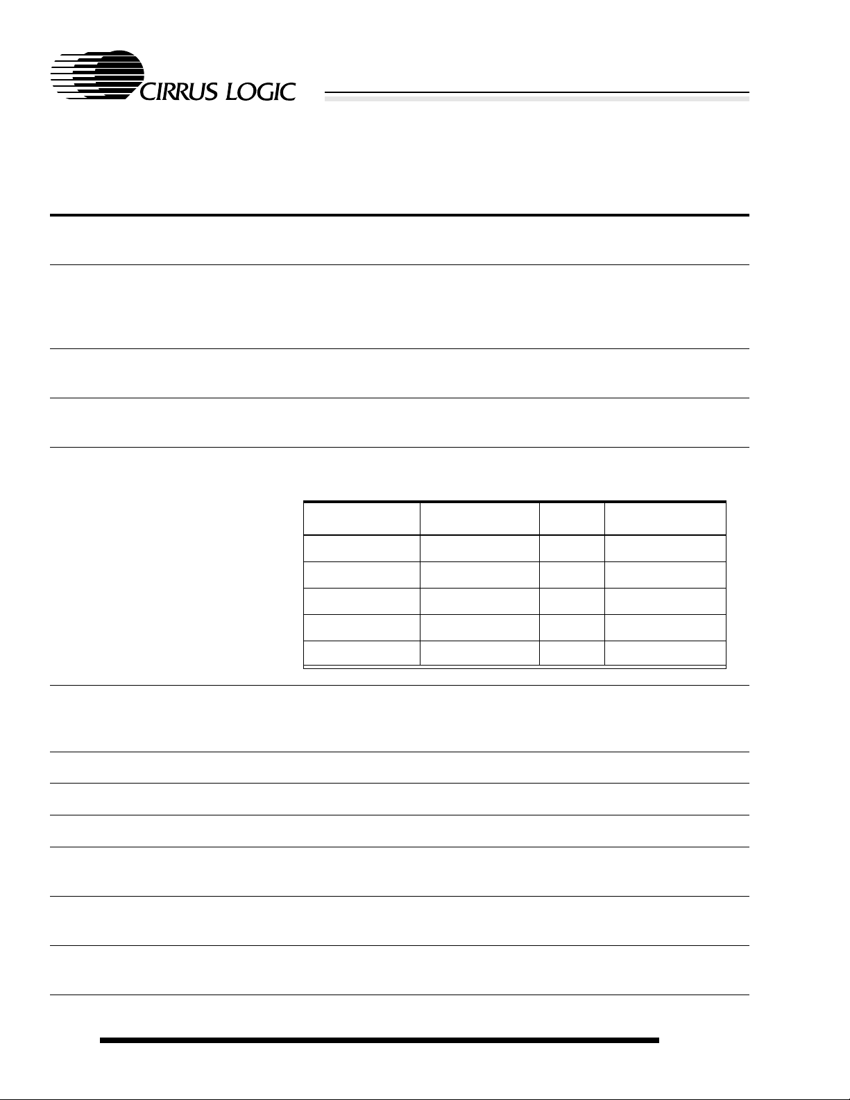
COLOR LCD
SVGA MONITOR
TV
HEADPHONES
CL-PS7500FE
240-PIN PQFP
2*PS/2 PORTS
2 ANALOG
INPUTS
VIDEO O/P
(RGB)
AUDIO O/P
(32 BIT)
KEYBOARD MOUSE
GAMES DEVICE
(ANALOG)
FRONT PANEL:
STATUS LEDs
RUN/STANDBY SW
REALTIME CLOCK
CONFIG. MEMORY
(NON-VOL.)
DRAM
(4 MBYTE, TYP)
ROM
56k MODEM
CL-MD34XX
ETHERNET
CS89XX
ENCODER
PAL/NTSC
MEMORY BUS
I/O PORT
CD-DAC
CS4333
ISA-STYLE
BUS
■
■
■
■
CL-PS7500FE
Advance Data Book
FEATURES
Availab le in 56- and 40-MHz speed grades
System-on-a-chip solution
— 32-bit ARM7 processor with MMU
— 4K unified cache
— FPU (floating point unit)
— Graphics controller drives CRT or LCD
— CD-quality sound audio controller
— DRAM controller
— ROM/Flash controller
— Three-channel DMA for video, cursor, and sound
— PC-style I/O bus
— Two-state power management
— Eight general-purpose I/O lines
Performance
— 50 Vax -MIPS (Dhrystone
— Up to 12 Mflops, double-precision FP (LINPACK)
) at 56 MHz
FPU
— Implements ANSI/IEEE Std 754-1985
— Single, double, and e xtended precision
System-on-a Chip for
Internet Appliance
OVERVIEW
The Cirrus Logic CL-PS7500FE is designed to be
used in internet appliances such as the network
computer, smart-TV, intranet terminal, screen
phones, DVD play ers, and so on.
The massively integrated CL-PS7500FE offers a
complete system-on-a-chip solution that includes a
32-bit ARM CPU with cache and MMU, CRT and
LCD controller, memory controller , FPU, CD-quality
sound controller, interface to the Cirrus Logic DSP
device for 56K modem and speakerphone, and a
PC-type I/O bus. To handle streaming of audio and
video data on the Internet, the CL-PS7500FE
includes a double-precision FPU to accelerate
software codecs.
(cont.) (cont.)
Functional
Block Diagram
June 1997Version 2.0

■
■
■
■
■
CL-PS7500FE
System-on-a-Chip for Internet Appliance
FEATURES
CRT or color/monochrome LCDs
— Resolutions up to 1024 × 768
— 256-entry 28-bit video palette
— Single- and dual-scan panel LCDs (16-bit grayscale)
Serial CD digital sound (32-bit) output
Supports EDO and Fast page mode DRAMs
— Up to 132 Mbytes/sec. (peak) using 64-MHz memory
clock and 32-bit-wide DRAM
— Programmable 16- or 32-bit-wide memory system
— Speed-critical paths are pipelined
OVERVIEW
(cont.)
(cont.)
The video controller features RGB drive of a SVGA
monitor or a color LCD. It also incorporates various
sync inputs, which when combined with an external
encoder, permit the use of interlaced TV displays.
The device incorporates a digital audio controller
with a 32-bit serial interface for connection to the
Cirrus Logic, CS4333 CD-DAC device. The
CL-PS7500FE can also interface to the Cirrus Logic
56K, FastPath modem chipset ideal for Internet
access over a PO TS line .
PC-style I/O bus (40-MHz) for connection to any
Cirrus Logic peripheral device
— 56k fax/modem chipset
— CS89XX Ethernet controller
— Can be expanded to 32 bits with external transceivers
ROM/FLASH
— Supports two 16-Mbyte banks
— Individual read timings
— Burst mode reads
— Allows for writes under register control for FLASH
The CL-PS7500FE supports UMA (unified memory
architecture); EDO DRAMs can be used to achieve
high-memory bandwidth.
The CL-PS7500FE is the main computing engine in
the NC platform defined by Oracle
, and runs the
NC operating system and applications.
The device is available in a 240-pin PQFP (plastic
quad flat pack) package.
The CL-PS7500FE is availab le in two speed grades:
●
ARM CPU running at 40 MHz; memory clock
running up to 64 MHz
●
ARM CPU running at 56 MHz; memory clock
running up to 64 MHz
2
ADVANCE DATA BOOK v2.0
June 1997

CL-PS7500FE
System-on-a-Chip for Internet Appliance
3
ADVANCE DATA BOOK v2.0
June 1997

CL-PS7500FE
System-on-a-Chip for Internet Appliance
TABLE OF CONTENTS
CONVENTIONS .....................................................................................................................12
1. PIN INFORMATION...............................................................................................................13
1.1 Pin Diagram......................................................................................................................................13
1.2 Block Diagram..................................................................................................................................14
2. PIN DESCRIPTIONS.............................................................................................................15
2.1 CL-PS7500FE Pin Descriptions .......................................................................................................15
2.2 Power and Ground Pins....................................................................................................................22
2.3 Numerical Pin Listing........................................................................................................................24
3. FUNCTIONAL DESCRIPTION..............................................................................................27
3.1 Functional Block Diagram.................................................................................................................27
3.2 ARM Processor Macrocell................................................................................................................27
3.3 FPA Macrocell...................................................................................................................................27
3.4 Video and Sound Macrocell..............................................................................................................29
3.5 Clock Control and Power Management............................................................................................29
3.6 Memory System ...............................................................................................................................29
3.6.1 DMA..................................................................................................................................30
3.6.2 I/O Control........................................................................................................................30
3.7 Other Features .................................................................................................................................31
3.8 Test Modes.......................................................................................................................................31
3.9 Structure of the CL-PS7500FE.........................................................................................................31
3.9.1 Register Programming......................................................................................................32
3.9.2 Interaction Between Macrocells........................................................................................32
3.10 Resetting CL-PS7500FE Systems ...................................................................................................32
4. THE ARM PROCESSOR MA CROCELL..............................................................................33
4.1 Architecture ......................................................................................................................................33
4.2 Instruction Set ..................................................................................................................................33
4.3 Memory Interface..............................................................................................................................34
4.4 Clocks and Synchronous/Asynchronous Modes..............................................................................34
5. IDC .........................................................................................................................................35
5.1 Cacheable Bit...................................................................................................................................35
5.2 IDC Operation...................................................................................................................................35
5.2.1 IDC V alidity.......................................................................................................................35
5.2.2 Software IDC Flush...........................................................................................................35
5.2.3 Doubly-Mapped Space.....................................................................................................35
5.2.4 Read-Locked-Write...........................................................................................................36
5.3 IDC Enable/Disable and Reset.........................................................................................................36
5.3.1 Enable the IDC.................................................................................................................36
5.3.2 Disable the IDC.................................................................................................................36
5.4 Write Buffer (WB) .............................................................................................................................36
5.4.1 Bufferable Bit ....................................................................................................................36
5.4.2 Write Buffer Operation......................................................................................................36
5.4.3 Enable the Write Buffer.....................................................................................................37
5.4.4 Disable the Write Buffer....................................................................................................37
5.5 Coprocessors ...................................................................................................................................37
June 1997
ADVANCE DATA BOOK v2.0
TABLE OF CONTENTS
3

CL-PS7500FE
System-on-a-Chip for Internet Appliance
6. ARM PROCESSOR MMU.................................................................................................... 38
6.1 MMU Program-Accessible Registers................................................................................................38
6.1.1 Translation Table Base Register ......................................................................................39
6.1.2 Domain Access Control Register......................................................................................39
6.1.3 Fault Status Register........................................................................................................39
6.1.4 Fault Address Register.....................................................................................................39
6.2 Address Translation..........................................................................................................................39
6.3 Translation Process..........................................................................................................................40
6.3.1 TTB (Translation Table Base)............................................................................................40
6.3.2 Level One Fetch................................................................................................................40
6.3.3 Level One Descriptor........................................................................................................41
6.3.4 P age Table Descriptor.......................................................................................................41
6.3.5 Section Descriptor............................................................................................................42
6.4 Translating Section References........................................................................................................42
6.4.1 Lev el Two Descriptor.........................................................................................................42
6.5 Translating Small Page References..................................................................................................44
6.6 Translating Large Page References.................................................................................................45
6.7 MMU Faults and CPU Aborts...........................................................................................................47
6.8 Fault Address and Fault Status Registers (FAR, FSR).....................................................................47
6.9 Domain Access Control....................................................................................................................48
6.10 Fault-Checking Sequence................................................................................................................48
6.10.1 Alignment Fault.................................................................................................................49
6.10.2 Translation Fault................................................................................................................50
6.10.3 Domain Fault ....................................................................................................................50
6.10.4 Permission Fault...............................................................................................................50
6.11 External Aborts.................................................................................................................................50
6.11.1 Interaction of the MMU, IDC, and Write Buffer..................................................................51
7. REGISTER DESCRIPTIONS................................................................................................ 52
7.1 Register Configuration......................................................................................................................52
7.1.1 Big and Little Endian (the Bigend Bit)...............................................................................52
7.1.2 Configuration Bits for Backward Compatibility..................................................................53
7.2 Operating Mode Selection................................................................................................................54
7.3 Registers ..........................................................................................................................................55
7.3.1 PSRs (Program Status Registers)....................................................................................56
7.4 Exceptions........................................................................................................................................57
7.4.1 FIQ....................................................................................................................................57
7.4.2 IRQ...................................................................................................................................58
7.4.3 Abort.................................................................................................................................58
7.4.4 Software Interrupt.............................................................................................................59
7.4.5 Undefined Instruction Trap................................................................................................60
7.4.6 Vector Summary...............................................................................................................60
7.4.7 Exception Priorities...........................................................................................................61
7.4.8 Interrupt Latencies............................................................................................................61
7.4.9 Reset................................................................................................................................61
7.5 Configuration Control Registers .......................................................................................................62
7.5.1 Backward Compatibility ....................................................................................................62
7.5.2 Internal Coprocessor Instructions.....................................................................................62
7.5.3 Registers ..........................................................................................................................63
7.6 Register 1: Control (Write only)........................................................................................................64
4
TABLE OF CONTENTS
ADVANCE DATA BOOK v2.0
June 1997

CL-PS7500FE
System-on-a-Chip for Internet Appliance
7.7 Register 2: Level One Page Table (Write only).................................................................................64
7.8 Register 3: Domain Access Control (Write only)..............................................................................64
7.9 Register 4: Reserved........................................................................................................................64
7.10 Register 5: Fault Status/Translation Lookaside Buffer Flush ............................................................65
7.11 Register 6: Fault Address/TLB Purge...............................................................................................65
7.12 Register 7: IDC Flush (Write only)....................................................................................................65
7.13 Registers 8–15: Reserved................................................................................................................65
8. MEMORY MAP......................................................................................................................66
9. MEMORY SUBSYSTEMS.....................................................................................................67
9.1 ROM Interface..................................................................................................................................67
9.1.1 ROM Bank Configuration and Timing ...............................................................................68
9.2 DRAM Interface................................................................................................................................69
9.2.1 DRAM Control Registers..................................................................................................69
9.2.2 DRAM Address Multiplexing............................................................................................70
9.2.3 Selection Between 16- and 32-bit DRAM.........................................................................70
9.2.4 EDO and Timing Mode Selection .....................................................................................71
9.2.5 DRAM Refresh..................................................................................................................72
9.2.6 DRAM Self-Refresh..........................................................................................................73
9.2.7 Non-Sequential Access Time and RAS Precharge ..........................................................73
9.3 DMA Channels .................................................................................................................................74
9.3.1 Video DMA.......................................................................................................................74
9.3.2 Cursor DMA.....................................................................................................................75
9.3.3 Sound DMA.....................................................................................................................75
9.3.4 The Sound DMA State Machine.......................................................................................76
10. MEMORY AND I/O PROGRAMMERS’ MODEL...................................................................78
10.1 Introduction.......................................................................................................................................78
10.2 Register Summary............................................................................................................................78
10.3 Register Descriptions .......................................................................................................................81
10.3.1 IOCR (0x00) — I/O Control...............................................................................................81
10.3.2 KBDDAT (0x04) — Keyboard Data...................................................................................81
10.3.3 KBDCR (0x08) — Keyboard Control.................................................................................82
10.3.4 IOLINES (0x0C) — IOP[7:0] Port Control.........................................................................83
10.3.5 IRQSTA (0x10) — IRQ A Interrupts Status.......................................................................83
10.3.6 IRQRQA (0x14) — IRQ A Interrupts Request/Clear.........................................................84
10.3.7 IRQMSKA (0x18) — IRQ A Interrupts Mask.....................................................................84
10.3.8 SUSMODE (0x1C) — SUSPEND Mode...........................................................................85
10.3.9 IRQSTB (0x20) — IRQ B Interrupts Status ......................................................................85
10.3.10 IRQRQB (0x24) — IRQ B Interrupts Request ..................................................................86
10.3.11 IRQMSKB (0x28) — IRQ B Interrupts Mask.....................................................................86
10.3.12 STOPMODE (0x2C) — STOP Mode................................................................................87
10.3.13 FIQST (0x30) — FIQ Interrupts Status.............................................................................87
10.3.14 FIQRQ (0x34) — FIQ Interrupts Request.........................................................................87
10.3.15 FIQMSK (0x38) — FIQ Interrupts Mask ...........................................................................88
10.3.16 CLKCTL (0x3C) — Clock Control.....................................................................................88
10.3.17 T0low (0x40) — Timer 0 Low Bits.....................................................................................89
10.3.18 T0high (0x44) — Timer 0 High Bits...................................................................................89
10.3.19 T0GO (0x48) — Timer 0 Go Command............................................................................89
10.3.20 T0LAT (0x4C) — Timer 0 Latch Command.......................................................................89
June 1997
ADVANCE DATA BOOK v2.0
TABLE OF CONTENTS
5

CL-PS7500FE
System-on-a-Chip for Internet Appliance
10.3.21 T1low (0x50) — Timer 1 Low Bits.....................................................................................89
10.3.22 T1high (0x54) — Timer 1 High Bits ..................................................................................89
10.3.23 T1GO (0x58) — Timer 1 Go Command............................................................................90
10.3.24 T1LAT (0x5C) — Timer 1 Latch Command ......................................................................90
10.3.25 IRQSTC (0x60) — IRQ C Interrupts Status......................................................................90
10.3.26 IRQRQC (0x64) — IRQ C Interrupts Request..................................................................90
10.3.27 IRQMSKC (0x68) — IRQ C Interrupts Mask ....................................................................90
10.3.28 VIDMUX (0x6C) — Video LCD and Serial Sound MUX Control.......................................91
10.3.29 IRQSTD (0x70) — IRQ D Interrupts Status......................................................................91
10.3.30 IRQRQD (0x74) — IRQ D Interrupts Request..................................................................92
10.3.31 IRQMSKD (0x78) — IRQ D Interrupts Mask ....................................................................92
10.3.32 ROMCR1:0 (0x80 and 0x84) — ROM Control..................................................................93
10.3.33 REFCR (0x8C) — Refresh Period....................................................................................94
10.3.34 ID0 (0x94) — Chip ID Number (Low Byte) .......................................................................94
10.3.35 ID1 (0x98) — Chip ID Number (High Byte) ......................................................................94
10.3.36 VERSION (0x9C) — Chip Version Number......................................................................94
10.3.37 MSEDAT (0xA8) — Mouse Data.......................................................................................94
10.3.38 MSECR (0xAC) — Mouse Control....................................................................................95
10.3.39 IOTCR (0xC4) — I/O Timing Control ................................................................................95
10.3.40 ECTCR (0xC8) — I/O Expansion Card Timing Control....................................................95
10.3.41 ASTCR (0xCC) — I/O Asynchronous Timing Control.......................................................96
10.3.42 DRAMCR (0xD0) — DRAM Control .................................................................................96
10.3.43 SELFREF (0xD4) — DRAM Self-Refresh Control............................................................97
10.3.44 ATODICR (0xE0) — A-to-D Interrupt Control ...................................................................97
10.3.45 ATODSR (0xE4) — A-to-D Status ....................................................................................98
10.3.46 ATODCC (0xE8) — A-to-D Convertor Control..................................................................98
10.3.47 ATODCNT1 (0xEC) — A-to-D Counter 1..........................................................................99
10.3.48 ATODCNT2 (0xF0) — A-to-D Counter 2...........................................................................99
10.3.49 ATODCNT3 (0xF4) — A-to-D Counter 3...........................................................................99
10.3.50 ATODCNT4 (0xF8) — A-to-D Counter 4...........................................................................99
10.3.51 SDCURA (0x180) — Sound DMA Current A....................................................................99
10.3.52 SDENDA (0x184) — Sound DMA End A........................................................................100
10.3.53 SDCURB (0x188) — Sound DMA Current B..................................................................100
10.3.54 SDENDB (0x18C) — Sound DMA End B.......................................................................101
10.3.55 SDCR (0x190) — Sound DMA Control...........................................................................102
10.3.56 SDST (0x194) — Sound DMA Status.............................................................................102
10.3.57 CURSCUR (0x1C0) — Cursor DMA Current .................................................................103
10.3.58 CURSINIT (0x1C4) — Cursor DMA INIT........................................................................103
10.3.59 VIDCURB (0x1C8) — Duplex LCD Video DMA Current B .............................................103
10.3.60 VIDCURA (0x1D0) — Video DMA Current A..................................................................104
10.3.61 VIDEND (0x1D4) — Video DMA End.............................................................................104
10.3.62 VIDSTART (0x1D8) — Video DMA Start........................................................................104
10.3.63 VIDINITA (0x1DC) — Video DMA INIT A........................................................................105
10.3.64 VIDCR (0x1E0) — Video DMA Control...........................................................................106
10.3.65 VIDINITB (0x1E8) — Duplex LCD Video DMA INIT B....................................................107
10.3.66 DMAST/DMARQ/DMAMSK (0x1F0,0x1F4,0x1F8) — DMA Interrupt Control................108
6
TABLE OF CONTENTS
ADVANCE DATA BOOK v2.0
June 1997

CL-PS7500FE
System-on-a-Chip for Internet Appliance
11. I/O SUBSYSTEMS ..............................................................................................................109
11.1 Introduction.....................................................................................................................................109
11.2 I/O Address Space Usage..............................................................................................................109
11.3 Additional I/O Chip Select Decode Logic........................................................................................110
11.4 Simple 8-MHz I/O ...........................................................................................................................111
11.5 Module I/O......................................................................................................................................111
11.6 PC Bus-Style I/O ............................................................................................................................111
11.7 DMA During I/O Cycles ..................................................................................................................114
11.8 Clock Synchronization Conditions..................................................................................................114
11.9 Keyboard/mouse Interface..............................................................................................................114
11.10 Analog-to-Digital Converter Interface .............................................................................................116
11.10.1 Counters.........................................................................................................................116
11.10.2 Interrupt Control..............................................................................................................116
11.10.3 Status of Interface...........................................................................................................117
11.10.4 Control............................................................................................................................118
11.10.5 Comparators...................................................................................................................118
11.10.6 Converter Operation.......................................................................................................118
11.11 Timers.............................................................................................................................................119
11.11.1 Programming the Timers ................................................................................................120
11.11.2 Timer interrupts ..............................................................................................................120
11.12 General-Purpose, 8-bit-wide, I/O Port ............................................................................................120
11.13 ID and OD Open-Drain I/O Pins .....................................................................................................121
11.14 Version and ID Registers................................................................................................................121
11.15 Interrupt Control .............................................................................................................................121
12. VIDEO FEATURES..............................................................................................................124
12.1 Pixel Clock......................................................................................................................................124
12.2 Palette ............................................................................................................................................126
12.2.1 Palette Updating.............................................................................................................126
12.3 Cursor.............................................................................................................................................126
12.3.1 Cursor in HiRes Mode ....................................................................................................127
12.3.2 Cursor in LCD Mode.......................................................................................................127
12.4 HiRes Support................................................................................................................................127
12.4.1 CL-PS7500FE Support for HiRes Mode.........................................................................127
12.5 Liquid Crystal Displays ...................................................................................................................129
12.5.1 LCD Grayscaling.............................................................................................................129
12.5.2 Dual-Panel LCDs (Duplex Mode)....................................................................................129
12.5.3 Single-Panel Color LCDs................................................................................................130
12.6 External Support.............................................................................................................................130
12.6.1 ECLK ..............................................................................................................................131
12.6.2 Power Saving Considerations.........................................................................................131
12.6.3 Vertical and Horizontal Synchronization.........................................................................131
12.6.4 GENLOCK......................................................................................................................131
12.7 Analog Outputs...............................................................................................................................131
12.7.1 DAC Control....................................................................................................................131
12.7.2 Pedestal Current.............................................................................................................132
12.7.3 Video DAC Currents .......................................................................................................132
12.7.4 Monochrome Output.......................................................................................................132
June 1997
ADVANCE DATA BOOK v2.0
TABLE OF CONTENTS
7

CL-PS7500FE
System-on-a-Chip for Internet Appliance
13. SOUND FEATURES ........................................................................................................... 133
13.1 Sound.............................................................................................................................................133
13.2 The Sound FIFO.............................................................................................................................133
13.3 The Digital Serial Sound Interface..................................................................................................133
13.3.1 Timing Formats...............................................................................................................133
14. VIDEO AND SOUND MACR OCELL.................................................................................. 135
14.1 Features .........................................................................................................................................135
14.1.1 Flexible Video System ....................................................................................................135
14.1.2 Hardware Cursor ............................................................................................................135
14.1.3 Palette.............................................................................................................................135
14.1.4 Pixel Clock......................................................................................................................136
14.1.5 Display Modes................................................................................................................136
14.1.6 Power Management........................................................................................................136
14.1.7 On-chip Sound System...................................................................................................136
15. VIDEO MACR OCELL INTERFACE.................................................................................... 138
15.1 Bus Interface ..................................................................................................................................138
15.2 Setting the FIFO Preload Value......................................................................................................138
15.2.1 Example..........................................................................................................................139
16. THE VIDEO SOUND AND PROGRAMMER’S MODEL.................................................... 140
16.1 The Video and Sound Macrocell Registers....................................................................................140
16.2 Video Palette: Address 0x0............................................................................................................142
16.3 Video Palette Address Pointer: Address 0x1..................................................................................142
16.4 LCD Offset Registers: Addresses 0x30 and 0x31..........................................................................143
16.5 Border Color Register: Address 0x4...............................................................................................144
16.6 Cursor Palette: Addresses 0x5–0x7...............................................................................................144
16.7 Horizontal Cycle Register (HCR): Address 0x80............................................................................145
16.8 Horizontal Sync Width Register (HSWR): Address 0x81................................................................145
16.9 Horizontal Border Start Register (HBSR): Address 0x82...............................................................145
16.10 Horizontal Display Start Register (HDSR): Address 0x83..............................................................146
16.11 Horizontal Display End Register (HDER): Address 0x84...............................................................146
16.12 Horizontal Border End Register (HBER): Address 0x85 ................................................................146
16.13 Horizontal Cursor Start Register (HCSR): Address 0x86...............................................................147
16.14 Horizontal Interlace Register (HIR): Address 0x87.........................................................................147
16.15 Horizontal Test Registers: Addresses 0x88 and 0x8H....................................................................147
16.16 Vertical Cycle Register (VCR): Address 0x90................................................................................147
16.17 Vertical Sync Width Register (VSWR): Address 0x91 ....................................................................148
16.18 Vertical Border Start Register (VBSR): Address 0x92....................................................................148
16.19 Vertical Display Start Register (VDSR): Address 0x93...................................................................148
16.20 Vertical Display End Register (VDER): Address 0x94....................................................................149
16.21 Vertical Border End Register (VBER): Address 0x95.....................................................................149
16.22 Vertical Cursor Start Register (VCSR): Address 0x96....................................................................149
16.23 Vertical Cursor End Register (VCER): Address 0x97.....................................................................150
16.24 Vertical Test Registers: Addresses 0x98, 0x9A and 0x9C..............................................................150
16.25 External Register (EREG): Address 0xC........................................................................................151
16.26 Frequency Synthesizer Register (FSYNREG): Address 0xD .........................................................152
16.27 Control Register (CONREG): Address 0xE....................................................................................153
16.28 Data Control Register (DCTL): Address 0xF..................................................................................154
16.29 Sound Frequency Register (SFR): Address 0xB0..........................................................................154
16.30 Sound Control Register (SCTL): Address 0xB1.............................................................................155
8
TABLE OF CONTENTS
ADVANCE DATA BOOK v2.0
June 1997

CL-PS7500FE
System-on-a-Chip for Internet Appliance
17. FPA COPROCESSOR MACROCELL ................................................................................156
17.1 FPA Functional Blocks....................................................................................................................157
17.1.1 Coprocessor Interface ....................................................................................................157
17.1.2 Instruction Issuer ............................................................................................................157
17.1.3 The Load-Store Unit .......................................................................................................157
17.1.4 The Register Bank..........................................................................................................157
17.1.5 The Arithmetic Unit.........................................................................................................158
18. FLOATING-POINT COPROCESSOR PROGRAMMER’S MODEL...................................160
18.1 Overview.........................................................................................................................................160
18.1.1 Floating-Point Status Register........................................................................................160
18.1.2 Floating-Point Control Register.......................................................................................160
18.2 Floating-Point Operation.................................................................................................................160
18.3 ARM Integer and Floating-Point Number Formats .........................................................................161
18.3.1 Integer.............................................................................................................................161
18.3.2 IEEE Single Precision (S)...............................................................................................161
18.3.3 IEEE Double Precision (D) .............................................................................................161
18.3.4 IEEE Extended Double Precision (E) .............................................................................162
18.3.5 Packed Decimal (P)........................................................................................................163
18.3.6 Expanded Packed Decimal (EP).....................................................................................163
18.4 The Floating-Point Status Register (FPSR)....................................................................................164
18.4.1 System ID Byte...............................................................................................................164
18.4.2 Exception Trap Enable Byte............................................................................................165
18.4.3 System Control Byte.......................................................................................................165
18.4.4 Cumulative Exception Flags Byte...................................................................................166
18.5 The Floating-Point Control Register (FPCR)..................................................................................168
19. FLOATING-POINT INSTRUCTION SET.............................................................................170
19.1 Coprocessor Data Transfer.............................................................................................................170
19.1.1 LDF/STF — Load and Store Floating.............................................................................170
19.1.2 Assembler Syntax...........................................................................................................171
19.1.3 Load and Store Multiple Floating Instructions ................................................................172
19.1.4 Assembler Syntax — Form 1..........................................................................................173
19.1.5 Assembler Syntax — Form 2..........................................................................................174
19.2 Coprocessor Data Operations........................................................................................................174
19.2.1 Dyadic Operations..........................................................................................................174
19.2.2 Monadic Operations........................................................................................................175
19.2.3 Library Calls....................................................................................................................175
19.2.4 Backwards Compatibility.................................................................................................175
19.3 Coprocessor Register Transfer.......................................................................................................178
19.3.1 Compare Operations ......................................................................................................179
19.4 FPA Instruction Set........................................................................................................................180
19.4.1 Infinities and NaNs..........................................................................................................180
19.4.2 Exceptional Conditions...................................................................................................180
19.5 Floating-point Support Code ..........................................................................................................182
19.5.1 IEEE Standard Conformance .........................................................................................182
19.6 Instruction Cycle Timing .................................................................................................................183
19.6.1 Instruction Classification.................................................................................................184
19.6.2 Perf ormance Tuning........................................................................................................185
June 1997
ADVANCE DATA BOOK v2.0
TABLE OF CONTENTS
9

CL-PS7500FE
System-on-a-Chip for Internet Appliance
20. BUS INTERFACE................................................................................................................ 187
20.1 Bus Arbitration................................................................................................................................187
20.2 Bus Cycle Types.............................................................................................................................187
20.3 Video DMA Bandwidth....................................................................................................................188
20.4 Video DMA Latency........................................................................................................................188
21. CLOCKS, POWER SAVING, AND RESET........................................................................ 191
21.1 Clock Control..................................................................................................................................191
21.1.1 Video and Sound Subsystem Clocks..............................................................................191
21.1.2 I/O Clock Outputs...........................................................................................................191
21.1.3 Synchronous/Asynchronous Mode for the ARM Processor............................................191
21.1.4 Clock Prescalars.............................................................................................................192
21.1.5 Clocking Schemes..........................................................................................................192
21.2 Power Management........................................................................................................................192
21.2.1 SUSPEND Mode............................................................................................................193
21.2.2 STOP Mode....................................................................................................................194
21.3 Reset..............................................................................................................................................195
22. ELECTRICAL SPECIFICATIONS ...................................................................................... 196
22.1 Absolute Maximum Ratings............................................................................................................196
22.2 DC Specifications...........................................................................................................................197
22.2.1 DC Specifications — Digital Values................................................................................197
22.3 Derating..........................................................................................................................................198
22.4 AC Parameters — List of Timing Figures .......................................................................................199
22.5 System Reset Timing .....................................................................................................................200
22.6 Memory Subsystems......................................................................................................................201
22.7 I/O Subsystems..............................................................................................................................209
22.8 System Timing (Clocks)..................................................................................................................222
23. P A CKA GE........................................................................................................................... 225
23.1 240-Pin PQFP Package Example...................................................................................................225
24. ORDERING INFORMATION EXAMPLE............................................................................ 226
10
TABLE OF CONTENTS
ADVANCE DATA BOOK v2.0
June 1997

CL-PS7500FE
System-on-a-Chip for Internet Appliance
Appendixes
A. INITIALIZATION AND BOOT SEQUENCE........................................................................227
1. Introduction.....................................................................................................................................227
2. Sample Boot Sequence..................................................................................................................227
3. Other Methods................................................................................................................................228
B. DUAL-PANEL LIQUID CRYSTAL DISPLAYS...................................................................229
1. Programming the Video Subsystem...............................................................................................229
2. Configuring DMA within the CL-PS7500FE....................................................................................230
3. Cursor.............................................................................................................................................230
4. Video Frame Buffer Restrictions.....................................................................................................231
C. USING ASTCR AT HIGH MEMCLK FREQUENCIES........................................................232
1. Using ASTCR.................................................................................................................................232
2. ASTCR I/O Cycle Type and Hold Times.........................................................................................233
3. Example..........................................................................................................................................233
D. EXPANDING PC-STYLE I/O TO 32 BITS ..........................................................................234
1. 32-Bit I/O ........................................................................................................................................234
E. CL-PS7500FE VIDEO CLOCK SOUR CES.........................................................................236
1. Introduction.....................................................................................................................................236
2. Clock Sources ................................................................................................................................236
3. Using the Phase Comparator.........................................................................................................237
4. Phase Comparator Reset...............................................................................................................240
4.1 Reset Procedure.............................................................................................................240
F . CL-PS7500FE TEST MODES..............................................................................................241
1. Introduction.....................................................................................................................................241
2. Test Modes Description ..................................................................................................................241
G. CL-PS7500FE PINOUT DIFFERENCES FROM THE ARM7500 ......................................243
1. Introduction.....................................................................................................................................243
INDEX .................................................................................................................................245
June 1997
ADVANCE DATA BOOK v2.0
TABLE OF CONTENTS
11
CL-PS7500FE
System-on-a-Chip for Internet Appliance
CONVENTIONS
Abbreviations
Symbol Units of measure
bpp bits-per-pixel
°C degree Celsius
Hz hertz (cycles per second)
Kbyte kilobyte (1,024 bytes)
kHz kilohertz
kΩ kilohm
Mbyte megabyte (1,048,576 bytes)
MHz megahertz (1,000 kilohertz)
µF microfarad
µs microsecond (1,000 nanoseconds)
mA milliampere
ms millisecond (1,000 microseconds)
ns nanosecond
pV picovolt
qword quad word
The use of ‘tbd’ indicates values that are ‘to be
determined’; ‘n/a’ designates ‘not available’; ‘n/c’
indicates a pin that is a ‘no connect’.
Acronyms
Acronym Definition
Acronym Definition
DRAM dynamic random-access memory
DVD digital video disk
EDO extended data out
FIFO first in/first out
FPA floating point accelerator
FPU floating point unit
GPIO general-purpose IO
HBM human body model
IC integrated circuit
IDC instruction and data cache
ISA industry standard architecture
LSB least-significant bit
LUT lookup table
MFLOPS million floating points per second
MMU memory management unit
MSB most-significant bit
MUX multiplexer
NaN not a number
PC program counter
PLL phased-locked loop
PQFP plastic quad-flat pack
RAM random-access memory
RISC reduced instruction set computer
ROM read-only memory
(cont.)
AC alternating current
ALU arithmetic logic unit
AP access permissions
A-to-D analog-to-digital
BIOS basic input/output system
CISC complex instruction set computer
CMOS
CRT cathode ray tube
DAC digital-to-analog converter
DC direct current
DMA direct memory access
12
CONVENTIONS
complementary metal-oxide semiconductor
R/W read/write
SRAM static random-access memory
SWI software interrupt instruction
TLB translation look-aside buffer
TTB translation table base
UMA unified memory architecture
VCO voltage-controlled oscillator
VRAM video random-access memory
WB write buffer
XIP execute-in-place
ADVANCE DATA BOOK v2.0
June 1997
CL-PS7500FE
System-on-a-Chip for Internet Appliance
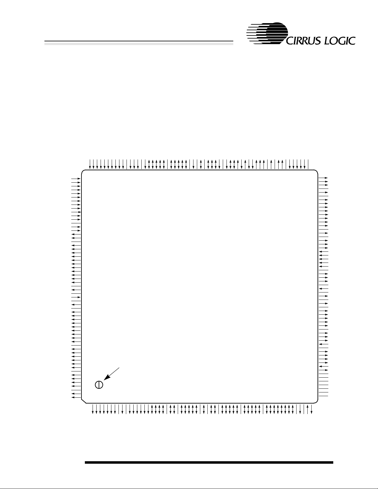
1. PIN INFORMATION
The CL-PS7500FE is available in a 240-pin PQFP (plastic quad flat pack) configuration.
1.1 Pin Diagram
ID
IOP0
IOP1
IOP2
IOP3
IOP4
IOP5
IOP6
IOP7
nPOR
VSSKBDATA
KBCLK
MSDATA
VDDMSCLK
BD0
BD1
BD2
BD3
BD4
VSSBD5
BD6
BD7
BD8
BD9
VDD_CORE
MEMCLK
VSS_CORE
BD10
VDDBD11
BD12
BD13
nEVENT2
VSSI_OCLK
BD14
BD15
nROMCS
nRESET
RESET
SnA
OSCDELAY
OSCPOWER
nWE
nCAS0
VDDnCAS1
VSSnCAS2
nCAS3
VSS_ATOD
ATOD0
ATOD1
ATOD2
180
179
178
177
176
175
174
173
172
171
170
169
168
167
166
165
164
163
162
161
160
159
158
157
156
155
154
153
152
151
150
149
148
147
146
145
144
143
142
141
140
139
138
137
136
135
134
133
132
131
130
129
128
127
126
125
OD1
OD0
SETCS
INT9
nINT4
INT5
READY
nIOGT
nBLI
nXIPMUX16
nINT1
INT2
nEVENT1
nXIPLATCH
nSIOCS2
V
nSIOCS1
nEASCS
nMSCS
nBLO
nRBE
nWBE
CLK2
REF8M
CLK8
CLK16
nIORQ
V
nIOR
VSS_CORE
CPUCLK
VDD_CORE
nIOW
V
nCCS
nCDACK
IORNW
nPCCS2
nPCCS1
LNBW
LA0
LA1
LA2
V
LA3
LA4
LA5
LA6
LA7
LA8
V
LA9
LA10
LA11
LA12
V
LA13
LA14
181
182
183
184
185
186
187
188
189
190
191
192
V
193
SS
194
195
TC
196
197
198
DD
199
200
201
202
203
204
205
206
207
208
209
210
SS
211
212
213
214
215
216
DD
217
218
219
220
221
222
223
224
225
226
SS
227
228
229
230
231
232
233
DD
234
235
236
237
238
SS
239
240
1234567891011121314151617181920212223242526272829303132333435363738394041424344454647484950515253545556575859
Pin 1 indicator
CL-PS7500FE
240-Pin PQFP
124
ATOD3
ATODREF
123
122
VDD_ATOD
121
120
119
118
117
116
115
114
113
112
111
110
109
108
107
106
105
104
103
102
101
100
99
98
97
96
95
94
93
92
91
90
89
88
87
86
85
84
83
82
81
80
79
78
77
76
75
74
73
72
71
70
69
68
67
66
65
64
63
62
61
60
nRAS0
nRAS1
nRAS2
V
DD
nRAS3
V
SS
RA0
RA1
RA2
RA3
RA4
RA5
RA6
RA7
V
DD
RA8
V
SS
RA9
RA10
RA11
INT7
nINT6
nINT3
nINT8
nTEST
VSS_ANALOG
GOUT
BOUT
ROUT
VDD_ANALOG
VIREF
VDD_CORE
HSYNC
VSS_CORE
VSYNC
V
SS
ED0
ED1
ED2
ED3
ED4
V
DD
ED5
ED6
ED7
HCLK
V
SS
ECLK
SYNC
WS
SDCLK
SCLK
SDO
VSS_CORE
V
SS
VDD_CORE
V
SS
V
SS
V
DD
V
DD
LA17
LA18
LA19
LA20
LA21
V
LA22
LA23
LA24
LA25
LA26
LA27
LA28
LA15
LA16
June 1997 13
ADVANCE DATA BOOK v2.0 PIN INFORMATION
SS
DD
V
D31
D30
D29
D28
SS
DD
V
V
D27
D26
D25
D24
D23
D22
D21
VSS_CORE
D20
D19
VDD_CORE
D18
SS
V
D17
D16
D15
D14
D13
DD
V
D12
D11
D10
D9
SS
D8
D7D6D5D4D3D2D1
V
SS
DD
D0
V
V
VCLKI
VCLKO
PCOMP
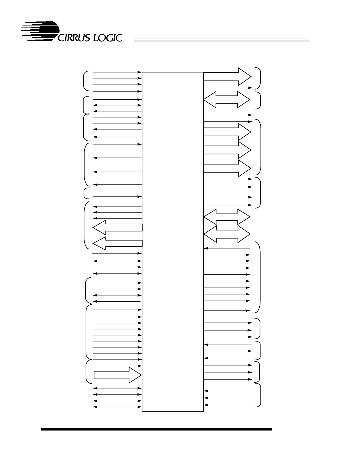
1.2 Block Diagram
CL-PS7500FE
System-on-a-Chip for Internet Appliance
MAIN
CLOCKS/CONTROL
RESET
VIDEO
CLOCKS AND
CONTROL
SOUND
SYSTEM
REFERENCE
CURRENT
VIDEO
OUTPUTS
POWER
MANAGEMENT
EXTERNAL
INTERRUPT
SOURCES
A-TO-D
CONVERTORS
KBD/MOUSE
INTERFACE
SNA
CPUCLK
MEMCLK
I_OCLK
nPOR
nRESET
RESET
HCLK
VCLKI
VCLKO
PCOMP
SCLK
WS
SDO
SDCLK
VIREF
HSYNC
VSYNC
ECLK
ED[7:0]
RGB OUTPUTS
nTEST
OD[1:0]
SYNC
ID
nEVENT1
nEVENT2
OSCDELAY
OSCPOWER
nINT6
nINT3
nINT8
INT7
INT9
nINT4
INT5
nINT1
INT2
ATODREF
ATOD[3:0]
MSECLK
MSEDAT
KBCLK
KBDAT
CL-PS7500FE
LA[28:0]
LNBW
D[31:0]
nROMCS
nWE
RA[11:0]
nCAS[3:0]
nRAS[3:0]
CLK2
CLK8
REF8M
CLK16
IOP[7:0]
BD[15:0]
SETCS
nCCS
nCDACK
TC
nPCCS2
nPCCS1
nSIOCS1
nMSCS
nEASCS
nSIOCS2
nBLO
nWBE
nRBE
nBLI
nIORQ
nIOGT
nIOR
nIOW
IORNW
nXIPLATCH
nXIPMUX16
READY
LATCHED
ADDRESS
BUS AND
DATA
BUS
I/O CHIP
SELECTS
I/O R/W
CONTROL
PIN INFORMATION
ADVANCE DATA BOOK v2.0
June 199714

CL-PS7500FE
System-on-a-Chip for Internet Appliance
2. PIN DESCRIPTIONS
This chapter gives the name, type, and relevant details of each of the CL-PS7500FE signals.
NOTE: When output signals are placed in the high-impedance state for long periods, ensure that they do not ‘float’
to an undefined logic level.
The following abbreiviations are used to indicate signal types.
IC
OCZ
IT Input, TTL threshold
ICS Input, CMOS Schmitt
IA Input, analog
OA Output, analog
BTZ Bidirectional, CMOS output, TTL threshold input level
TOD Open-drain, TTL input
CSOD Open-drain, CMOS schmitt input
IAOD Input, analog with programmable internal pull-down transistor
Input, CMOS threshold
Output, CMOS levels, tristate
For outputs and bidirectional signals, drive strength is classified 1, 2, or 3. See Chapter 22 for DC and AC
characteristics.
2.1 CL-PS7500FE Pin Descriptions
Name Type
LA[28:0] OCZ 2 LATCHED ADDRESS BUS: This bus is the latched version of the
Drive
Strength
Description
ARM address for memory accesses, changing on the falling edge of
the internal MCLK signal.
LNBW OCZ 2 LA TCHED NO T BYTE WORD: This is a latched v ersion of the inter-
nal NBW signal from the ARM processor, changing on the falling
edge of the internal MCLK signal.
D[31:0] BTZ 2 DATA: The main data bus for the CL-PS7500FE. All exter nal data
transfers happen through this bus. When the CL-PS7500FE is configured for operation in 16-bit mode, only the lo wer 16 bits are used.
SnA IC SYNCHRONOUS/NOT ASYNCHRONOUS: This pin is set accord-
ing to the relationship required between the internal clock signals,
MCLK and FCLK, for the ARM.
If this pin is set high, both the memory system and the CPU are
driven from the MEMCLK pin, and the required synchronous timing
relationship between the ARM processor clocks is generated automatically on-chip. If different clocks are to be used for the MEMCLK
and CPUCLK inputs, the SnA pin must be set low.
June 1997 15
ADVANCE DATA BOOK v2.0 PIN DESCRIPTIONS

CL-PS7500FE
System-on-a-Chip for Internet Appliance
2.1 CL-PS7500FE Pin Descriptions
Name Type
Drive
Strength
(cont.)
Description
BOUT AO BLUE ANALOG OUTPUT: The video signal analog outputs are
designed to drive doubly-terminated 75-Ω lines.
ECLK OCZ 3 EXTERNAL CLOCK: When enabled, this clock validates the data
on ED[7:0]. In normal video mode, it runs at the pix el rate , but when
LCD data is being produced, it runs at a quarter of the pixel rate.
ED[7:0] OCZ 2 EXTERNAL DATA: This is the digital video output port of the
CL-PS7500FE. From this, the digital equivalent of the analog output
can be produced in any color , or data from the external palette may
be produced. This can be used for a variety of purposes such as
fading or supremacy. Also, data for driving LCD panels is output
from this port. Data produced is validated b y ECLK.
GOUT AO GREEN ANALOG OUTPUT: The video signal analog outputs are
designed to drive doubly-terminated 75-Ω lines.
HCLK IT HIGH SPEED CLOCK: This is the clock used with video sub-
system.
HSYNC OCZ 3 HORIZONTAL SYNCHRONIZATION: There are two synchroniza-
tion outputs on
the CL-PS7500FE, HSYNC and VSYNC . Dependent
on the state of bits 17 and 16 in the video External register, either a
horizontal or a composite (NOR) sync can be output on this pin, in
either polarity . The width of the HSYNC pulse is definable in units of
2 pixels.
PCOMP OCZ 1 PHASE COMPARATOR OUTPUT: Used with VCLK pins.
ROUT AO RED ANALOG OUTPUT: The video signal analog outputs are
designed to drive doubly-terminated 75-Ω lines.
SCLK IT SOUND CLOCK: This signal can be used to clock the sound sys-
tem, when a clock asynchronous to the internal video reference
clock is required.
SDCLK OCZ 2 SERIAL DA TA CLOCK: This clock v alidates serial sound data on its
rising edge.
SDO OCZ 2 SERIAL DATA OUT: Serial sound data is output from this pin.
SYNC IT EXTERNAL SYN: This signal is used to synchronize CL-PS7500FE
with another video system.
VCLKI IC PHASE COMPARATOR CLOCK IN (for video subsystem).
VCLKO OCZ 2 PHASE COMPARATOR CLOCK OUT (for video subsystem).
PIN DESCRIPTIONS
ADVANCE DATA BOOK v2.0
June 199716

CL-PS7500FE
System-on-a-Chip for Internet Appliance
2.1 CL-PS7500FE Pin Descriptions
Name Type
Drive
Strength
(cont.)
Description
VIREF IA VIDEO REFERENCE CURRENT: The video DACs need a refer-
ence current to calibrate them. A constant current source is recommended, although a resistor up to V
is sufficient for many
DD
applications. This current also generates the constant source f or the
A-to-D comparators.
VSYNC OCZ 3 VERTICAL SYNCHRONIZATION: Dependent on the state of bits
19 and 18 in the external register, either a ver tical or a composite
(XNOR) sync can be output on this pin, in either polarity. The width
of the VSYNC pulse can be defined in units of a raster.
WS OCZ 2 WORD SELECT: This signal denotes whether the output serial data
is for the left-hand or right-hand stereo channel.
nTEST IT TEST MODE INPUT: This pin should be held permanently high. It
is only intended to be used during production test of the
CL-PS7500FE. An on-chip pull-up resistor is included, but it is
advised to apply an external pull-up resistor to this pin.
nWE OCZ 2 WRITE ENABLE: This is a active-low signal.
RA[11:0] OCZ 2 DRAM ROW/COLUMN MULTIPLEXED ADDRESS BUS:
Addresses for this bus are decoded from the ARM processor
address for normal memory accesses, and are generated by the
DMA controller for DMA.
nRAS[3:0] OCZ 3 DRAM ROW ADDRESS STROBES: Each of these selects one of
the four banks of DRAM available.
nCAS[3:0] OCZ 3 DRAM COLUMN ADDRESS STROBES: These select the byte
within the word for DRAM accesses.
ATOD[3:0] IAOD ANALOG-TO-DIGITAL: These are the four A-to-D channel input
voltages.
ATODREF IA ANALOG-TO-DIGITAL REFERENCE: This is the reference v oltage
for the A-to-D converter comparators.
OSCPOWER OCZ 1 OCILLA TOR PO WER: This is the enab le signal for the system oscil-
lator(s). When low, this signal can be used to disable the external
oscillator(s).
OSCDELAY CSOD 1 OCILLATOR DELAY: This signal requires an RC netw ork to gener-
ate a fixed delay when restarting the system oscillator(s) on exit
from STOP mode.
June 1997 17
ADVANCE DATA BOOK v2.0 PIN DESCRIPTIONS
CL-PS7500FE
System-on-a-Chip for Internet Appliance
2.1 CL-PS7500FE Pin Descriptions
Name Type
Drive
Strength
(cont.)
Description
RESET OCZ 2 RESET OUTPUT: This is the synchronized version of internal sys-
tem reset signal.
nRESET CSOD 2 RESET: This is an open-drain output and a ‘soft’ reset input. This pin
is sampled every 1µs for reset events, so to guarantee a successful
reset, a reset pulse applied to this pin must be longer than 1µs (1µs,
assuming the internal I/O clock is 32 MHz).
nROMCS OCZ 1 ROM CHIP SELECT: This signal goes low to indicate a ROM
access.
I_OCLK IC I/O SYSTEM CLOCK: This clock input should always be 32 MHz
when in Divide-by-1 mode, and 64 MHz in Divide-by-2 mode.
MEMCLK IC MEMORY SYSTEM CLOCK: In synchronous mode, the ARM pro-
cessor FCLK is also driven from this clock.
CPUCLK [MHz] MEMCLK [MHz] SnA Notes
Low 40 High
40 56 Low
40 64 Low
Low 56 High Recommended
56 64 Low
CPUCLK IC This clock creates FCLK for the ARM CPU in asynchronous mode.
When SnA is high, this signal should be permanently tied high or
low.
BD[15:0] BTZ 2 This is the main external 16-bit I/O bus.
MSCLK TOD 2 MOUSE CLOCK: An open-drain pin for the mouse PS/2 interface.
MSDATA TOD 2 MOUSE DATA: An open-drain pin for the mouse PS/2 interface.
KBCLK TOD 2 KEYBOARD CLOCK: An open-drain pin for the keyboard PS/2
interface.
KBDATA TOD 2 KEYBOARD DATA: An open-drain pin for the keyboard PS/2 inter-
face.
nPOR ICS POWER ON RESET: Any low transitions on this pin are detected
and stretched to ensure a full reset.
PIN DESCRIPTIONS
ADVANCE DATA BOOK v2.0
June 199718

CL-PS7500FE
System-on-a-Chip for Internet Appliance
2.1 CL-PS7500FE Pin Descriptions
Name Type
Drive
Strength
(cont.)
Description
IOP[7:0] TOD 1 I/O PORT : This is the 8-bit-wide I/O port. Each bit is directly control-
lable through an CL-PS7500FE register, and can be used as an
interrupt source if required.
ID TOD 1 ID: This pin activates a system ID chip. It is forced low during the
power-on reset sequence.
OD[1:0] TOD 1 OPEN DRAIN 1:0: These are the tw o open-drain pins, which (unlike
the IOP[7:0] bus) cannot be used to generate interrupts, but can be
used as general-purpose I/O pins (for example to communicate with
a realtime clock chip).
SETCS IC This signal selects between two address decoding options for the
three main I/O chip selects. It aff ects the outputs nEASCS , nMSCS,
and nSIOCS2.
nINT1 IT This is a falling-edge-triggered interrupt. The nINT1 value can be
read directly in the IOCR I/O control register.
INT2 IT This is a rising-edge-triggered interrupt pin that can generate an
IRQ interrupt.
nINT3 IT This is an active-low interrupt that can generate an IRQ interrupt.
nINT4 IT This is an active-low interrupt that can generate an IRQ interrupt.
INT5 IT This is an active-high interrupt that can generate either an IRQ or a
FIQ interrupt, depending on the status of the relevant mask register
bits.
nINT6 IT This is an active-low interrupt that can generate either an IRQ or a
FIQ interrupt, depending on the programming of the mask registers.
INT7 IT This is an active-high interrupt that can generate an IRQ interrupt.
nINT8 IT This is an active-low interrupt that can generate either a FIQ or an
IRQ interrupt.
INT9 IT This is an active-high interrupt that can only generate a FIQ (highest
priority) interrupt.
nEVENT1 IT This is the active-low asynchronous event pin 1. A falling edge ter-
minates the STOP or SUSPEND power-saving modes.
nEVENT2 IT This is the active-low asynchronous event pin 2. A falling edge ter-
minates the STOP or SUSPEND power-saving modes.
June 1997 19
ADVANCE DATA BOOK v2.0 PIN DESCRIPTIONS

CL-PS7500FE
System-on-a-Chip for Internet Appliance
2.1 CL-PS7500FE Pin Descriptions
Name Type
Drive
Strength
(cont.)
Description
READY IT READY: This pin can stretch I/O accesses when set low during a
16-MHz PC-type I/O cycle.
nIORQ OCZ 2 I/O REQUEST: This signal is for the module-type I/O for handshak-
ing, together with nIOGT.
nIOGT IT I/O GRANT: This signal is for the module-type I/O f or handshaking,
together with nIORQ.
nBLI IT This input is used during module-type I/O reads to cause the latch-
ing of data from the BD port.
nBLO OCZ 1 This signal is the latching signal for use with external latches on the
upper 16 bits of the external datapath to create a 32-bit-wide I/O
bus.
nRBE OCZ 1 This active-low read enable is used to create a 32-bit-wide I/O bus
for an external transceiver attached to the upper 16 bits of the I/O
bus.
nWBE OCZ 1 This active-low write enable is used to create a 32-bit-wide I/O bus
for an external transceiver attached to the upper 16 bits of the I/O
bus.
nXIPMUX16 IT This signal is for XIP (execute in place) suppor t. This signal multi-
plexes 16 bits of data from the upper or lower halfword of the
CL-PS7500FE internal data bus to the 16-bit I/O bus, depending on
its state during writes.
nXIPLATCH IT This signal is for XIP support and latches the upper 16 bits of data
from the I/O bus while the lower 16 bits are being read. This signal
is used in conjunction with nXIPMUX16 to enable XIP (for e xample ,
from a 16-bit PCMCIA card).
nSIOCS1 OCZ 1 This is the active-low chip select for simple I/O.
nSIOCS2 OCZ 1 This is the active-low chip select f or simple I/O, with address decode
modified according to the state of SETCS.
nMSCS OCZ 2 This is the active-low chip select for module-type I/O, with address
decode modified according to the state of SETCS.
nEASCS OCZ 1 This is the active-low chip select for extended 16-MHz PC-type I/O,
with address decode modified according to the state of SETCS.
nCCS OCZ 1 NOT COMBO CHIP SELECT: This is the chip select signal for a PC
Combo chip.
PIN DESCRIPTIONS
ADVANCE DATA BOOK v2.0
June 199720

CL-PS7500FE
System-on-a-Chip for Internet Appliance
2.1 CL-PS7500FE Pin Descriptions
Name Type
Drive
Strength
(cont.)
Description
nCDACK OCZ 1 NOT COMBO DACK: This is the chip select and DACK signal for a
PC Combo chip.
TC OCZ 1 TERMINAL COUNT: This active-high signal is used in conjunction
with the nCDACK signal for pseudo DMA to a PC Combo chip.
nPCCS1 OCZ 1 This is the active-low chip select for an area of 16-MHz PC-type I/O
space.
nPCCS2 OCZ 1 This is the active-low chip select for an area of 16-MHz PC-type I/O
space.
LNBW OCZ 2 LA TCHED NO T BYTE WORD: This is a latched version of the inter-
nal NBW signal from the ARM processor, which transitions on the
falling edge of the internal MCLK signal.
IORNW OCZ 2 I/O READ/NOT WRITE: This signal goes high during an I/O read,
and low during an I/O write.
nIOR OCZ 2 NOT I/O READ: This signal has two functions:
1) It transitions low during simple and PC-type I/O reads; not used for
module-type I/O.
2) It is asserted low during ROM read cycles to act as an output
enable.
nIOW OCZ 2 NOT I/O WRITE: This signal has two functions:
1) It transitions low during simple and PC-type I/O reads; not used for
module-type I/O.
2) It is asserted low during writes to ROM space, to act as a write
enable, if writes are enabled in the ROMCR register.
CLK2 OCZ 2 This is the 2-MHz I/O clock output.
CLK8 OCZ 2 This is the 8-MHz I/O clock output, the inverted version of REF8M.
REF8M OCZ 2 This is the 8-MHz I/O clock output.
CLK16 OCZ 2 This is the 16-MHz I/O clock output, for PC-type I/O.
June 1997 21
ADVANCE DATA BOOK v2.0 PIN DESCRIPTIONS

System-on-a-Chip for Internet Appliance
2.2 Power and Ground Pins
Name Pin No. Description
CL-PS7500FE
V
DD
8
24
These 15 pins supply +5 volts to the digital logic of the CL-PS7500FE. Each pin
must be connected to the V
CC
plane.
41
56
61
62
79
106
117
132
149
166
198
216
233
V
SS
10
21
These 20 pins supply the ground reference to the digital logic of the
CL-PS7500FE. Each pin must be connected to the ground plane.
35
47
58
63
64
66
74
85
104
115
130
144
159
170
193
210
226
238
VDD_CORE 32
65
89
153
214
PIN DESCRIPTIONS
These five pins supply +5 volts to the core logic of the CL-PS7500FE. Each pin
must be connected to the V
CC
plane.
ADVANCE DATA BOOK v2.0
June 199722

CL-PS7500FE
System-on-a-Chip for Internet Appliance
2.2 Power and Ground Pins
Name Pin No. Description
VSS_CORE 30
67
These five pins supply the ground ref erence to the core logic. Each pin must be
connected to the ground plane.
(cont.)
87
151
212
VDD_ATOD 121 This pin is the positive (+5V) supply for the A-to-D converter comparators. This
pin must be connected directly to the V
plane.
CC
VSS_ATOD 127 This pin is the analog ground for the A-to-D converter comparators. This pin
must be connected to the ground plane.
VDD_Analog 91 This pin supplies the positive (+5V) supply for analog video system. This pin
must be connected directly to the V
CC
plane.
VSS_Analog 95 This pin supplies ground for analog video system. This pin must be connected
to the ground plane.
June 1997 23
ADVANCE DATA BOOK v2.0 PIN DESCRIPTIONS
System-on-a-Chip for Internet Appliance
2.3 Numerical Pin Listing
The following table is a numeric listing of the pins of the CL-PS7500FE.
CL-PS7500FE
Pin number Signal name
1 LA[15]
2 LA[16]
3 LA[17]
4 LA[18]
5 LA[19]
6 LA[20]
7 LA[21]
8V
DD
9 LA[22]
10 V
SS
11 LA[23]
12 LA[24]
13 LA[25]
14 LA[26]
15 LA[27]
Pin number Signal name
30 VSS_CORE
31 D[20]
32 VDD_CORE
33 D[19]
34 D[18]
35 V
SS
36 D[17]
37 D[16]
38 D[15]
39 D[14]
40 D[13]
41 V
DD
42 D[12]
43 D[11]
44 D[10]
Pin number Signal name
59 VCLKI
60 VCLKO
61 V
62 V
63 V
64 V
DD
DD
SS
SS
65 VDD_CORE
66 V
SS
67 VSS_CORE
68 SDO
69 SCLK
70 SDCLK
71 WS
72 SYNC
73 ECLK
16 LA[28]
17 D[31]
18 D[30]
19 D[29]
20 D[28]
21 V
SS
22 D[27]
23 D[26]
24 V
DD
25 D[25]
26 D[24]
27 D[23]
28 D[22]
29 D[21]
PIN DESCRIPTIONS
45 D[9]
46 D[8]
47 V
SS
48 D[7]
49 D[6]
50 D[5]
51 D[4]
52 D[3]
53 D[2]
54 D[1]
55 D[0]
56 V
DD
57 PCOMP
58 V
SS
74 V
75 HCLK
76 ED[7]
77 ED[6]
78 ED[5]
79 V
80 ED[4]
81 ED[3]
82 ED[2]
83 ED[1]
84 ED[0]
85 V
86 VSYNC
87 VSS_CORE
ADVANCE DATA BOOK v2.0
SS
DD
SS
June 199724
CL-PS7500FE
System-on-a-Chip for Internet Appliance
Pin number Signal name
88 HSYNC
89 VDD_CORE
90 VIREF
91 VDD_ANALOG
92 ROUT
93 BOUT
94 GOUT
95 VSS_ANALOG
96 nTEST
97 nINT8
98 nINT3
99 nINT6
100 INT7
101 RA[11]
102 RA[10]
103 RA[9]
Pin number Signal name
120 nRAS[0]
121 VDD_ATOD
122 ATODREF
123 ATOD[3]
124 ATOD[2]
125 ATOD[1]
126 ATOD[0]
127 VSS_ATOD
128 nCAS[3]
129 nCAS[2]
130 V
SS
131 nCAS[1]
132 V
DD
133 nCAS[0]
134 nWE
135 OSCPOWER
Pin number Signal name
152 MEMCLK
153 VDD_CORE
154 BD[9]
155 BD[8]
156 BD[7]
157 BD[6]
158 BD[5]
159 V
SS
160 BD[4]
161 BD[3]
162 BD[2]
163 BD[1]
164 BD[0]
165 MSCLK
166 V
DD
167 MSDATA
104 V
SS
105 RA[8]
106 V
DD
107 RA[7]
108 RA[6]
109 RA[5]
110 RA[4]
111 RA[3]
112 RA[2]
113 RA[1]
114 RA[0]
115 V
SS
116 nRAS[3]
117 V
DD
118 nRAS[2]
119 nRAS[1]
136 OSCDELAY
137 SnA
138 RESET
139 nRESET
140 nROMCS
141 BD[15]
142 BD[14]
143 I_OCLK
144 V
SS
145 nEVENT2
146 BD[13]
147 BD[12]
148 BD[11]
149 V
DD
150 BD[10]
151 VSS_CORE
168 KBCLK
169 KBDATA
170 V
SS
171 nPOR
172 IOP[7]
173 IOP[6]
174 IOP[5]
175 IOP[4]
176 IOP[3]
177 IOP[2]
178 IOP[1]
179 IOP[0]
180 ID
181 OD[1]
182 OD[0]
183 SETCS
June 1997 25
ADVANCE DATA BOOK v2.0 PIN DESCRIPTIONS
CL-PS7500FE
System-on-a-Chip for Internet Appliance
Pin number Signal name
184 INT9
185 nINT4
186 INT5
187 READY
188 nIOGT
189 nBLI
190 nXIPMUX16
191 nINT1
192 INT2
193 V
SS
194 nEVENT1
195 nXIPLATCH
196 TC
197 nSIOCS2
198 V
DD
199 nSIOCS1
Pin number Signal name
216 V
DD
217 nCCS
218 nCDACK
219 IORNW
220 nPCCS2
221 nPCCS1
222 LNBW
223 LA[0]
224 LA[1]
225 LA[2]
226 V
SS
227 LA[3]
228 LA[4]
229 LA[5]
230 LA[6]
231 LA[7]
200 nEASCS
201 nMSCS
202 nBLO
203 nRBE
204 nWBE
205 CLK2
206 REF8M
207 CLK8
208 CLK16
209 nIORQ
210 V
SS
211 nIOR
212 VSS_CORE
213 CPUCLK
214 VDD_CORE
215 nIOW
232 LA[8]
233 V
DD
234 LA[9]
235 LA[10]
236 LA[11]
237 LA[12]
238 V
SS
239 LA[13]
240 LA[14]
PIN DESCRIPTIONS
ADVANCE DATA BOOK v2.0
June 199726

CL-PS7500FE
System-on-a-Chip for Internet Appliance
3. FUNCTIONAL DESCRIPTION
The CL-PS7500FE is a high-performance, low-power RISC-based single-chip computer built around an
ARM microprocessor core. To maximize the potential of the ARM processor macrocell, the CL-PS7500FE
contains memory and I/O control on-chip, enabling the direct connection of external memory devices and
peripherals with the minimum of external components. The FPA (floating-point accelerator) is also integrated, resulting in outstanding math performance.
NOTE: The CL-PS7500FE is based on the ARM7500FE architecture from ARM Ltd., U.K. (http://www.arm.com).
The CL-PS7500FE includes features that make it particularly suitable for low-po wer portable applications.
Both 32- and 16-bit-wide memory systems are suppor ted, allowing the design of a lower-cost 16-bitbased system. The CL-PS7500FE drives color CRT or color LCD panels. Monochrome single- or dualpanel LCDs with 16 levels of g reyscaling can also be driven. Power-management circuitry is included with
two power-saving states. The high level of integration achieved allows significant PCB area saving, and
results in a very cost-competitive system.
The CL-PS7500FE is also particularly suited to any application requiring high-quality video, sound, and
general I/O requirements, such as multimedia. The video controller provides up to 16 million colors from
a 256-entry palette, running at up to a 120-MHz pixel clock rate. The sound subsystem includes a serial
sound interface for CD-quality 32-bit sound. Four on-chip A-to-D converters allow the connection of analog joysticks or similar control devices. The clocking scheme is very flexible, allowing either a very cheap
system to be built using a single oscillator , or separate asynchronous clocks to be used f or the CPU, memory and I/O subsystems, which gives an extremely flexible system, able to take advantage of the fastest
available DRAM memory.
3.1 Functional Block Diagram
Figure 3-1 on page 28 presents a more detailed view of the functionality of the CL-PS7500FE single-chip
computer.
3.2 ARM Processor Macrocell
The ARM processor contains an ARM7 core with MMU, 4-Kbyte cache, and write buffer.
3.3 FPA Macrocell
The FPA is a fully IEEE-754 compliant floating-point accelerator, and supports single, double, and
extended precision formats. It is connected to the ARM through the coprocessor interface and provides
the same floating-point functionality as the FPA11.
Concurrent load/store and arithmetic units, and speculative ex ecution are emplo yed to giv e good floatingpoint performance.
June 1997 27
ADVANCE DATA BOOK v2.0 FUNCTIONAL DESCRIPTION
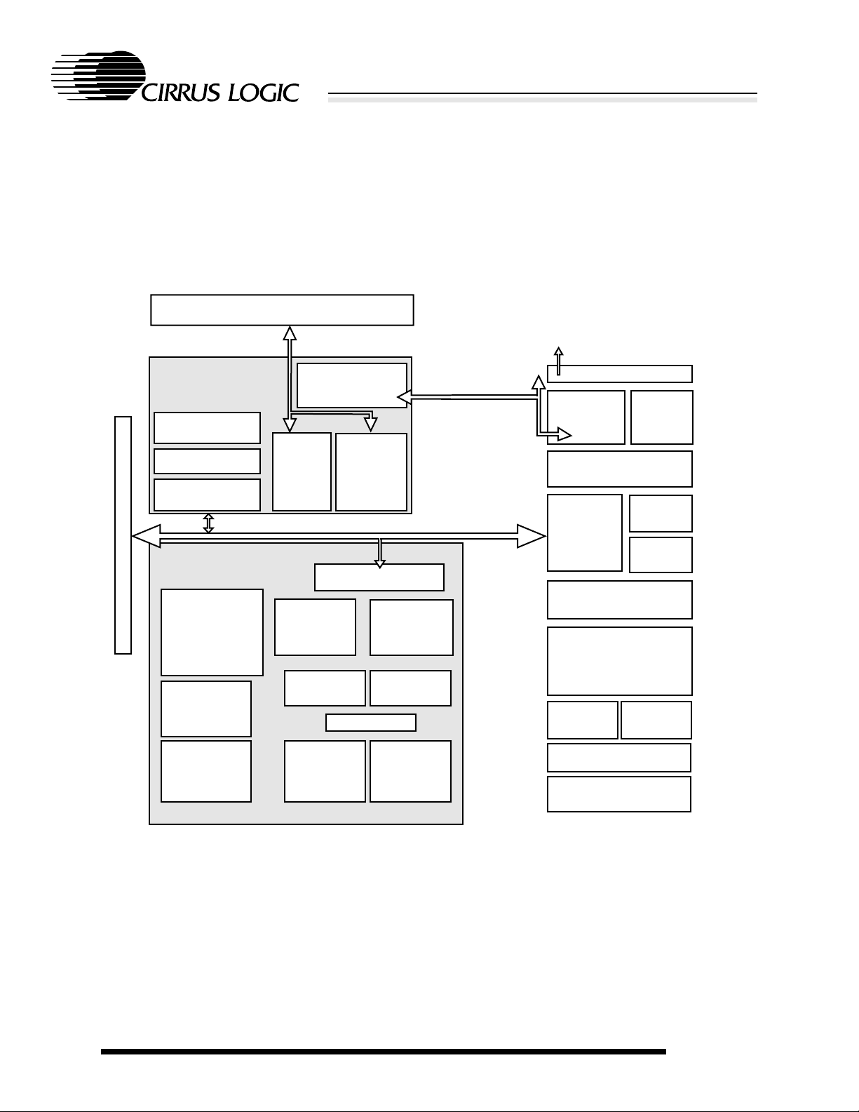
ARM PROCESSOR
MMU
FPA
ADDRESS
BUFFER
CL-PS7500FE
System-on-a-Chip for Internet Appliance
LATCHED ADDRESS
ADDRESS LATCH
INTERNAL
ADDRESS
ADDRESS
DECODE
I/O
CONTROL
WRITE BUFFER
D
A
T
A
P
A
T
H
DATA BUFFER
VIDEO AND SOUND
HORIZONTAL AND
VERTICAL TIMING
AND
CLOCK CONTROL
SOUND
FIFO
DIGITAL
SOUND
4-KBYTE
CACHE
INTERNAL DATA
VIDEO FIFO
AND
SERIALIZER
VIDEO
PALETTES
ANALOG
RGB
OUTPUTS
ARM7
CPU
DATA LATCH
CURSOR FIFO
AND
SERIALIZER
CURSOR
PALETTES
MUX
EXTERNAL
LCD
OUTPUTS
INTERRUPTS
AND TIMERS
SERIAL
AND
AND
RESET
CONTROL
PORT 1
SERIAL
PORT 2
DRAM
DATA
BUFFER
BUS CONTROL
ARBITRATION
CLOCK CONTROL,
POWER MANAGEMENT,
DMA
CONTROL
ROM CONTROL
4 A-TO-D
CONVERTORS
Figure 3-1. Functional Block Diagram of the CL-PS7500FE
FUNCTIONAL DESCRIPTION
ADVANCE DATA BOOK v2.0
June 199728

CL-PS7500FE
System-on-a-Chip for Internet Appliance
3.4 Video and Sound Macrocell
The video and sound macrocell gives the CL-PS7500FE the flexibility to drive high analog CRT or low
power LCD displays, and features the following:
● Up to 120-MHz pixel clock rate
● Resolutions of up to 1024 × 768 pixels are directly supported
(greater if external serialization is used)
● Fully programmable display parameters
● 256-entry by 28-bit video palette
● Red, green and blue 8-bit linear DACs to drive CRT
● 1-, 2-, 4-, 8-, 16-, and 32-bpp CRT modes
● Up to 16 million colors
● External bits in palette for supremacy, fading, HiRes
● Single- or dual-panel LCD driving
● 16-level gray scalar for LCD
● Power management features
● Hardware cursor for all display modes
● Sound system — serial CD digital output
3.5 Clock Control and Power Management
The clocking strategy for CL-PS7500FE has been designed f or maximum fle xibility , and includes separ ate
clock inputs for the:
● CPU core clock
● Memory system clock
● I/O system clock (in addition to the video clock inputs).
Each of the three clock inputs has a selectable divide-by-two prescalar to generate an internal 50/50
mark-space ratio if required. Throughout this data book, all timing diagrams assume that CPUCLK, MEMCLK, and I_OCLK are divided by one.
There are two levels of power management included:
● SUSPEND mode: The clock to the CPU is stopped, but the display continues to work normally, that is, DMA
unaffected.
● STOP mode: All clocks are stopped. Two asynchronous wake-up event pins are provided to terminate stop
mode. Circuitry is included on-chip to stop external oscillators and restart them cleanly when required.
3.6 Memory System
The memory system interface control logic is completely asynchronous in operation to the I/O control
logic. This means that the clock to the memory controller can be increased in frequency to allow faster
memory to be used. This implementation gives maximum system flexibility.
June 1997 29
ADVANCE DATA BOOK v2.0 FUNCTIONAL DESCRIPTION

CL-PS7500FE
System-on-a-Chip for Internet Appliance
The CL-PS7500FE can control a 32- or 16-bit-wide memory system. The width of each bank of ROM or
DRAM is selectable by programming appropriate register bits. Fast page mode or EDO DRAMs are supported.
A DRAM controller is included that can directly drive up to four banks of DRAM. Four nRAS strobes individually select one of the four banks, and f our nCAS strobes pro vide individual byte selection. The DRAM
address multiplexing option provided allows a wide variety of DRAM sizes to be used – from 256 Kbytes
to beyond 16 Mbytes . Up to 256 page mode transfers can occur in one sequential burst. When configured
for operation with a 16-bit-DRAM system, the DRAM controller conv erts the access into two DRAM cycles
to access the two halves of the 32-bit word. Byte transfers only take one DRAM access cycle, e v en in 16bit mode.
A programmable register allows one of four DRAM refresh rates to be selected. In addition, a register is
provided to enable direct software control of the nCAS and nRAS lines f or setting DRAM into a self-refresh
state.
A ROM controller supports two 16-Mbyte banks of ROM with individually programmable read cycle timings. Support is provided for b urst mode reads. Each ROM bank can be programmed to operate in 16-bitwide mode and, like the DRAM controller, converts accesses into two ROM cycles for the two halves of
the 32-bit word. The R OM controller can be programmed to allow write cycles through this interf ace, allowing FLASH to be programmed.
3.6.1 DMA
Three fully programmable DMA channels are included, for video, cursor, and sound data. The DMA controller includes additional support for dual-panel LCDs.
3.6.2 I/O Control
The I/O bus of the CL-PS7500FE is 16-bits wide, but for some types of access can be expanded to 32
bits by the use of external transceivers. The input clock I_OCLK provides a reference for the I/O subsystem nominally 32 MHz. The I/O features of this device can be separated into three distinct cycle types:
● Simple I/O with fixed 8-MHz timings
● Module I/O with variable length 8-MHz timings
● PC bus style I/O with fixed 16-MHz timings and support for 32-bit data
Simple I/O
The Simple I/O type of access is 16-bit-only and has a selection of four different cycle speeds selectable
by address. When writing, the upper half-word of the ARM data bus is written out on the I/O bus. When
reading, the I/O bus data is read back onto the lower half-word of the ARM data bus. During these
accesses, a chip select is asserted with the appropriate nIOR/nIOW read or write strobe, based on the
8-MHz clock CLK8.
Module I/O
The Module I/O type of access is 16 bits only and timing is controlled by a handshake mechanism with
the external hardware. The signals nIORQ (output) and nIOGT (input) are used for this handshaking and
are referenced to REF8M. When writing, the upper half-word of the ARM data bus is written out on the
I/O bus. When reading, the I/O bus data is read back onto the lower half-word of the ARM data bus.
FUNCTIONAL DESCRIPTION
ADVANCE DATA BOOK v2.0
June 199730

CL-PS7500FE
System-on-a-Chip for Internet Appliance
During these accesses, a chip select is asserted but the nIOR/nIOW read and write strobes are not used,
although the IORNW signal is active.
PC Bus Style I/O
The PC bus style I/O type of access routes the lower half-word of the ARM bus through the device providing a direct 16-bit interface. Signals are generated to support the addition of external latches/drivers to
extend the I/O data by 16 bits . The upper half-word of the ARM data bus is routed through these external
devices if present.
There are five different address areas that generate five different chip selects using the same type of
access. There are four fixed-cycle types based on the 16-MHz clock, although the largest area only supports two of these cycle types. Any access can be held up by external circuitry removing the READY signal before the end of the cycle.
During these accesses, the relevant chip select is asserted, as well as the appropriate read or wr ite
strobes.
Two special inputs are provided to allow external circuitry to route the full 32 bits through the 16-bit I/O
bus using multiplexing. This allows, for example, the execution of code from a 16-bit PCMCIA card with
suitable external controller . On a read I/O, if this latching signal is used, the data read back onto the ARM
data bus comes from the I/O bus instead of the external extension latches.
3.7 Other Features
The CL-PS7500FE includes four analog comparators used to create f our A-to-D con v erter channels, and
two serial keyboard/mouse ports.
There are eight general-purpose, open-drain I/O lines that can be used as inputs or open drain outputs
and, if required, as interrupt sources.
An interrupt handler processes a variety of internal and external interrupt sources to generate the IRQ
and FIQ interrupts for the ARM processor.
3.8 Test Modes
The CL-PS7500FE has an nTEST pin used to invoke various test modes. When nTEST is set low, the
functionality of many of the pins change depending on the values applied to the nINT3, nINT6 and nINT8
pins. The nTEST pin includes an on-chip pull-up resistor , but it is recommended that the pin be also pulled
up to V
NOTE: The nTEST pin should never be forced low during normal operation.
externally. See Appendix F.
DD
3.9 Structure of the CL-PS7500FE
The CL-PS7500FE includes three modified ARM macrocells:
● ARM processor
● FPA
● Video and sound macrocells
These macrocells are self-contained and the relevant control registers are contained within them. This
has the effect that there are four sets of programmable registers within the CL-PS7500FE, which are
accessed in different ways depending on their location.
June 1997 31
ADVANCE DATA BOOK v2.0 FUNCTIONAL DESCRIPTION

CL-PS7500FE
System-on-a-Chip for Internet Appliance
3.9.1 Register Programming
ARM processor register programming is described in Chapter 4. FPA register programming is described
in Chapter 18
The video and sound macrocell registers are programmed using only the internal CL-PS7500FE data bus
(the address bus is not passed to the macrocell). The address 0x03400000 is decoded to provide a write
strobe for the video macrocell registers, and the addressing of registers within the macrocell is decoded
from the upper four or eight bits of the data word. This system is described in more detail in Chapter 16.
The remaining CL-PS7500FE registers, associated with Memory , I/O , and general miscellaneous control,
form a separate group and are programmed between addresses 0x03200000 and 0x032001F8. The
majority of the registers are only 8 bits wide, although all register addresses are word-aligned. These registers are described in Chapter 7.
3.9.2 Interaction Between Macrocells
Interaction between the macrocells occurs mainly across the internal 32-bit data bus of the
CL-PS7500FE, which is routed to the ARM and video/sound macrocells, and most of the other memory
and I/O control logic. The address bus of the ARM processor is routed to an internal address decoder
where memory space is decoded to determine required cycle types and register addresses. The same
address bus is latched and exported from the device as the LA[28:0] bus. Only these 29 bits of the
address bus are available externally.
.
3.10 Resetting CL-PS7500FE Systems
The CL-PS7500FE is designed to operate with both 16- and 32-bit-wide ROMs, which means that it must
be capable of booting from either . To achiev e this, the de vice is alwa ys reset into 16-bit mode, which might
be expected to cause difficulty when the device is being booted up from 32-bit ROM. However,
Appendix A
under these circumstances.
describes a simple code sequence that allows the device to be started up without difficulty
FUNCTIONAL DESCRIPTION
ADVANCE DATA BOOK v2.0
June 199732

CL-PS7500FE
System-on-a-Chip for Internet Appliance
4. THE ARM PROCESSOR MACROCELL
The CL-PS7500FE contains a 32-bit RISC ARM processor, similar to the ARM710C macrocell. It has a
4-Kbyte cache, write buffer, and an MMU. The ARM processor macrocell offers high-level RISC performance, yet its fully static design ensures minimal power consumption. This makes it ideal f or incorporation
into the CL-PS7500FE. The CL-PS7500FE aims to make maximum use of the performance and flexibility
offered by the ARM processor.
This section describes the features of the ARM processor macrocell availab le to the user in its embedded
state within the CL-PS7500FE single-chip computer.
4.1 Architecture
The ARM processor architecture is based on RISC principles, and the instruction set and related decode
mechanism are greatly simplified compared with microprogrammed CISCs.
The mixed data and instruction cache, together with the write buffer, substantially raise the average execution speed and reduce the average amount of memory bandwidth required by the processor. This
allows the CL-PS7500FE bus structure to support DMA channels with minimal performance loss.
The MMU supports a conventional two-level page-table structure and a number of extensions, making it
ideal for embedded control, UNIX, and object-oriented systems.
4.2 Instruction Set
The instruction set comprises ten basic instruction types:
● Two instruction types make use of the on-chip ALU, barrel shifter, and multiplier to perform high-speed oper-
ations on the data in a bank of 31 registers, each 32 bits wide.
● Three classes of instruction control data transfers between memory and the registers:
— one optimized for flexibility of addressing,
— another for rapid context switching, and
— the third for swapping data.
● Two instructions control the flow and privilege level of execution.
● Three instruction types are dedicated to the control of coprocessors that allow the functionality of the instruc-
tion set to be extended in an open and uniform way; the on-chip FPA is one such processor.
However, the facility to add external coprocessors to the CL-PS7500FE is not available, and software emulation of coprocessor activity is required if instructions, other than those for the on-chip FPA or control coprocessor #15, are to perform a defined function.
The ARM instruction set is a good target for compilers of many different high-level languages. Where
required for critical code segments, assembly code programming is also straightforward, unlike some
RISC processors that depend on sophisticated compiler technology to manage complicated instruction
interdependencies.
June 1997 33
ADVANCE DATA BOOK v2.0 THE ARM PROCESSOR MACROCELL

CL-PS7500FE
System-on-a-Chip for Internet Appliance
4.3 Memory Interface
The memory interface has been designed to allow the performance potential to be realized without incurring high costs in the memory system. Speed-critical control signals are pipelined to allow system control
functions to be implemented in standard low-power logic, and these control signals permit the
CL-PS7500FE to exploit the page mode access offered by industry-standard DRAMs.
4.4 Clocks and Synchronous/Asynchronous Modes
The ARM processor uses two independent clock sources, MCLK and FCLK. Both are generated internally
to the CL-PS7500FE from MEMCLK and CPUCLK. The ARM7 core CPU switches between MCLK and
FCLK according to the operation being carried out. For example, if the ARM7 core CPU is reading data
from the cache, it is clocked by FCLK; if the core CPU is reading data from uncached memory then it is
clocked by MCLK. The control logic of the ARM processor ensures that the correct clock is used internally
and switches between the two clocks automatically.
When SnA is tied high, MEMCLK creates both FCLK and MCLK; MCLK has half the frequency of FCLK.
This synchronous mode ensures that there are no synchronization penalties whenever the ARM 7 core
is switched between FCLK and MCLK.
When SnA is tied low, MEMCLK creates MCLK and CPUCLK must be driven to supply FCLK. MEMCLK
and CPUCLK can be of unrelated frequency . There is a synchronization penalty whenev er the ARM7 core
clock switches between MCLK and FCLK. This penalty is symmetric, and varies between nothing and a
whole period of the clock where the core resynchronized. Thus, when changing there is an av erage resynchronization penalty of one-half a clock period, MCLK or FCLK as appropriate.
A[31:0] NR/W NB/W
ADDRESS BUFFER
MMU
WRITE
BUFFER
DBE
D[31:0]
INTERNAL ADDRESS BUS
4-KBYTE
CACHE
INTERNAL DATA BUS
CONNECTION TO
FPA COPROCESSOR
MCLK SNA FCLK NRESET
CLOCK
CONTROL
ARM7
CPU
CONTROL
COPROC
NMREQ
NIRQ
NFIQ
Figure 4-1. ARM Processor Block Diagram
THE ARM PROCESSOR MACROCELL
ADVANCE DATA BOOK v2.0
June 199734

CL-PS7500FE
System-on-a-Chip for Internet Appliance
5. IDC
ARM processor contains a 4-Kbyte mixed-instruction and data cache. The IDC has 256 lines of 16 bytes
(4 words), organized as a four-way set associative cache, and uses the virtual addresses generated by
the processor core. The IDC is always reloaded one line at a time (four words). It can be enabled or disabled through the ARM processor Control register and is disabled on nRESET.
The operation of the cache is further controlled by the
cacheable
or C bit stored in the Memory Management Page table (see the Section 6 on page 38). For this reason, to use the IDC the MMU must be
enabled. How e ver, the two functions can be enabled simultaneously with a single write to the Control register.
5.1 Cacheable Bit
The C bit determines whether data being read can be placed in the IDC and used for subsequent read
operations. Typically, main memor y is marked as cacheable to improve system perfor mance, and I/O
space as non-cacheable to stop the data being stored in the cache of the CL-PS7500FE. (For example,
if the processor is polling a hardware flag in I/O space, it is important that the processor is forced to read
data from the external peripheral, and not a copy of initial data held in the cache.) The Cacheable bit can
be configured for both pages and sections.
5.2 IDC Operation
In the ARM processor the cache is searched regardless of the state of the C bit, only reads that miss the
cache are affected.
● Cacheable reads
— C = 1: A line fetch of 4 words is performed and randomly placed in a cache bank.
● Uncacheable reads
— C = 0: An external memory access is performed and the cache is not written.
5.2.1 IDC V alidity
The IDC operates with virtual addresses, so ensure that the contents remain consistent with the virtualto-physical mappings performed by the MMU . If the memory mappings are changed, the IDC validity must
be ensured.
5.2.2 Software IDC Flush
The entire IDC can be marked as invalid by writing to the ARM processor IDC Flush register (register 7).
The cache is flushed immediately the register is written, but note that the next two instruction fetches ma y
come from the cache before the register is written.
5.2.3 Doubly-Mapped Space
Since the cache works with virtual addresses, it is assumed that every virtual address maps to a different
physical address. If the same physical location is accessed by more than one virtual address, the cache
cannot maintain consistency, since each virtual address has a separate entry in the cache, and only one
entry is updated on a processor write operation. To avoid an y cache inconsistencies, both doubly-mapped
virtual addresses should be marked as uncacheable.
June 1997 35
ADVANCE DATA BOOK v2.0 IDC

CL-PS7500FE
System-on-a-Chip for Internet Appliance
5.2.4 Read-Locked-Write
The IDC treats the Read-Locked-Write instruction as a special case. The read phase alwa ys forces a read
of external memory, regardless of whether the data is contained in the cache. The write phase is treated
as a normal write operation (and if the data is already in the cache, the cache is updated). Externally the
two phases are flagged as indivisible by asserting the LOCK signal.
5.3 IDC Enable/Disable and Reset
The IDC is automatically disabled and flushed on nRESET. Once enabled, cacheable read accesses
cause lines to be placed in the cache.
5.3.1 Enable the IDC
To enable the IDC, make sure that the MMU is enabled first by setting Control register, bit 0, then enable
the IDC by setting Control register, bit 2. The MMU and IDC can be simultaneously enabled with a single
control register write.
5.3.2 Disable the IDC
To disable the IDC, clear Control register, bit 2 and perform a flush by writing to the flush register.
5.4 Write Buffer (WB)
The ARM processor WB is provided to improve system performance. It can buffer up to 8 words of data,
and four independent addresses. It can be enabled or disabled through the W bit (bit 3) in the ARM processor Control register and the buffer is disabled and flushed on reset.
The operation of the write buffer is further controlled by one bit, B or
agement Page Tables. For this reason, to use the write buffer the MMU must be enabled.
The two functions may, howev er , be enabled sim ultaneously, with a single write to the Control register. For
a write to use the write buffer, both the W bit in the Control register, and the B bit in the corresponding
page table must be set.
5.4.1 Bufferable Bit
This bit controls whether a write operation may or may not use the write buffer. Typically main memory is
bufferable and I/O space unbufferable. The B bit can be configured for both pages and sections.
5.4.2 Write Buffer Operation
When the CPU performs a write operation, the translation entry for that address is inspected and the state
of the B bit determines the subsequent action. If the write buffer is disabled through the ARM processor
Control register, bufferable writes are treated in the same way as unbuffered writes.
buffer able
, stored in the Memory Man-
Bufferable Write
If the write buffer is enabled and the processor performs a write to a bufferable area, the data is placed in
the write buffer at FCLK speeds and the CPU continues execution. The write buffer then performs the
external write in parallel. If the write buffer is full (either because there are already 8 words of data in the
buffer , or because there is no slot f or the new address) then the processor is stalled until there is sufficient
space in the buffer.
IDC
ADVANCE DATA BOOK v2.0
June 199736

CL-PS7500FE
System-on-a-Chip for Internet Appliance
Unbufferable Writes
If the write buffer is disabled or the CPU perf orms a write to an unbuff erab le area, the processor is stalled
until the write buffer empties and the write completes externally. This process ma y require synchronization
and several external clock cycles.
Read-Locked Write
The write phase of a read-locked-write sequence is treated as an unbuffered write, even if it is marked as
buffered.
NOTE: A single write requires one address slot and one data slot in the write buffer; a sequential write of n words
requires one address slot and n data slots. The entire eight data slots in the buffer can be used as required.
So for instance there could be three non-sequential writes and one sequential write of 5 words in the buffer,
and the processor could continue as normal: a fifth write or a sixth word in the fourth write would stall the
processor until the first write is complete.
5.4.3 Enable the Write Buffer
To enable the WB, ensure the MMU is enabled by setting Control register, bit 0, then enable the write
buffer by setting Control register, bit 3. The MMU and write buffer can be enabled simultaneously with a
single write to the Control register.
5.4.4 Disable the Write Buffer
To disable the WB, clear the control register, bit 3.
NOTE: Any writes already in the write buffer completes normally.
5.5 Coprocessors
The on-chip FPA is a coprocessor and its operation are described later in this manual.
The ARM processor also has an internal coprocessor designated #15 for internal control of the device.
Howev er, the CL-PS7500FE has no external coprocessor bus, so it is not possible to add further external
coprocessors to this device. All coprocessor operations, other than those implemented by the FPA, MRC,
or MCR to registers 0–7 on coprocessor #15, cause the undefined instruction trap to be taken.
June 1997 37
ADVANCE DATA BOOK v2.0 IDC

CL-PS7500FE
System-on-a-Chip for Internet Appliance
6. ARM PROCESSOR MMU
The MMU performs two primary functions: it translates virtual addresses into physical addresses, and it
controls memory access permissions. The MMU hardware required to perform these functions consists
of a TLB, access control logic, and translation table walking logic.
The MMU supports memory accesses based on Sections or Pages:
● Sections are comprised of 1-Mbyte blocks of memory.
● Pages – two different page sizes are supported:
— Small pages consist of 4-Kbyte blocks of memory. Additional access control mechanisms are e xtended
within small pages to 1-Kbyte subpages.
— Large pages consist of 64-Kbyte bloc ks of memory . Additional access control mechanisms are extended
within large pages to 16-Kbyte subpages. Large pages are supported to allow mapping of a large region
of memory while using only a single entry in the TLB.
The MMU also supports the concept of domains — areas of memory that can be defined to possess individual access rights. The Domain Access Control register specifies access rights for up to 16 separate
domains.
The TLB caches 64 translated entries. During most memor y accesses, the TLB provides the translation
information to the access control logic. If the TLB contains a translated entry for the virtual address, the
access control logic determines whether access is permitted. If access is permitted, the MMU outputs
the appropriate physical address corresponding to the virtual address. If access is not permitted, the
MMU signals the CPU to abort.
If the TLB misses (that is, it does not contain a translated entry for the virtual address), the translation
table walk hardware is invoked to retrieve the translation information from a translation table in physical
memory . Once retrieved, the translation inf ormation is placed into the TLB , possibly ov erwriting an existing
value. The entry to be overwritten is chosen by cycling sequentially through the TLB locations.
When the MMU is turned off (for example, on reset), the virtual address is output directly onto the physical
address bus.
6.1 MMU Program-Accessible Registers
The ARM processor provides sev eral 32-bit registers that determine the operation of the MMU. The format
for these registers and a brief description is shown in Figure 6-1 on page 39. Each register is discussed
in more detail within the section that describes its use.
Data is written to and read from the MMU registers using the ARM CPU MRC and MCR coprocessor
instructions.
ARM PROCESSOR MMU
ADVANCE DATA BOOK v2.0
June 199738

CL-PS7500FE
System-on-a-Chip for Internet Appliance
EGISTER
1 WRITE
2 WRITE
3 WRITE
5 READ
5 WRITE
6 READ
6 WRITE
0 CONTROL 1 D P W ACM
TRANSLATION T ABLE BASE
DOMAIN ACCESS CONTROL
FAULT STATUS
FLUSH TLB
FAULT ADDRESS
TLB PURGE ADDRESS
R
SB
0 0 0 0 DOMAIN STATUS
012345678910111213141516171819202122232425262728293031
0123456789101112131415
Figure 6-1. MMU Register Summary
6.1.1 Translation Table Base Register
The Translation Table Base register contains the physical address of the base of the translation table
maintained in main memory. Note that this base must reside on a 16-Kbyte boundary.
6.1.2 Domain Access Control Register
The Domain Access Control register consists of sixteen 2-bit fields, each defines the access permissions
for one of the sixteen domains (D[15:0]).
NOTE: The registers not shown are reserved and should not be used.
6.1.3 Fault Status Register
The Fault Status register indicates the domain and type of access being attempted when an abort
occurred. Bits 7:4 specify the accessed of the sixteen domains (D[15:0]) during a fault. Bits 3:1 indicate
the type of access being attempted. The encoding of these bits is different for internal and external faults
(as indicated by bit 0 in the register) and is shown in Table 6-4 on page 47. A write to this register flushes
the TLB.
6.1.4 Fault Address Register
The Fault Address register holds the virtual address of the access attempted when a fault occurred. A
write to this register causes the data written to be treated as an address and, if it is found in the TLB, the
entry is marked as invalid. (This operation is known as a TLB ‘purge’.) The F ault Status and F ault Address
registers are only updated for data faults, not for prefetch faults.
6.2 Address T ranslation
The MMU translates virtual addresses generated by the CPU into physical addresses to access external
memory, and also derives and checks the access permission. Translation information, consisting of both
the address translation data and the access per mission data, resides in a translation table located in
physical memory. The MMU provides the logic needed to traverse this translation table, obtain
the translated address, and check the access permission.
June 1997 39
ADVANCE DATA BOOK v2.0 ARM PROCESSOR MMU

CL-PS7500FE
System-on-a-Chip for Internet Appliance
There are three routes for address translation and permission checking. The selected route depends on
if the address in question is marked as a section-mapped access or a page-mapped access; there are
two sizes of page-mapped access (large pages and small pages). However, the translation process
always starts out in the same way, as descr ibed in Section 6.3.2, with a Level One fetch. A sectionmapped access only requires a Level One fetch, but a page-mapped access also requires a Level Two
fetch.
6.3 Translation Process
6.3.1 TTB (Translation Table Base)
The translation process is initiated when the on-chip TLB does not contain an entry for the requested virtual address. The TTB register points to the base of a table in physical memory that contains Section
and/or Page descriptors. The 14 low-order bits of the TTB register are set to zero as illustrated in
Figure 6-2
,
the table must reside on a 16-Kbyte boundary.
TRANSLATION T ABLE BASE
0131431
Figure 6-2. Translation Table Base Register
6.3.2 Level One Fetch
Bits 31:14 of the TTB register are concatenated with bits 31:20 of the virtual address to produce a 30-bit
address, as illustrated in Figure 6-3. This address selects a 4-byte translation table entry that is a First
Level descriptor f or either a Section or a P age (bit 1 of the descriptor returned specifies if it is for a Section
or Page).
VIRTUAL ADDRESS
0192031
TABLE INDEX SECTION INDEX
TRANSLATION T ABLE BASE
031
12
031
00
TRANSLATION BASE
18
TRANSLATION BASE
1314
12
1314
TABLE INDEX
Figure 6-3. Accessing the Translation Table First Level Descriptors
ARM PROCESSOR MMU
FIRST LEVEL DESCRIPTOR
ADVANCE DATA BOOK v2.0
031
June 199740

CL-PS7500FE
System-on-a-Chip for Internet Appliance
6.3.3 Level One Descriptor
The Level One descriptor returned is either a Page Table descriptor or a Section descriptor , and the format
varies accordingly. Figure 6-4 illustrates the format of Level One descriptors.
01234589101112192031
0
0 FAULT
PAGE TABLE BASE ADDRESS
SECTION BASE ADDRESS 1
DOMAIN
DOMAINAP
1
CB
01
10
11
PAGE
SECTION
RESERVED
Figure 6-4. Level One Descriptors
The two least-significant bits indicate the descriptor type and validity, and are interpreted as in Table 6-1.
Table 6-1. Interpreting Level One Descriptor Bits 1:0
Value Meaning Notes
00 Invalid Generates a Section Translation fault.
01 Page Indicates that this is a Page descriptor.
10 Section Indicates that this is a Section descriptor.
11 Reserved Reserved for future use.
6.3.4 Page T able Descriptor
Bit Description
3:2 Always write as ‘0’.
4 Write as ‘1’ for backward compatibility.
8:5 Specify one of the sixteen possible domains (held in the Domain Access Control register) that contain the primary
access controls.
31:10 Form the base for referencing the Page Table entr y. (The page table index for the entry is derived from the virtual
address as illustrated in Figure 6-7 on page 45.)
If a Page Table descriptor is returned from the Lev el One f etch, a Lev el T wo f etch is initiated, as described
in the following section.
June 1997 41
ADVANCE DATA BOOK v2.0 ARM PROCESSOR MMU

6.3.5 Section Descriptor
Bit Description
CL-PS7500FE
System-on-a-Chip for Internet Appliance
3:2
(C, B)
4 Write as ‘1’ for backward compatibility.
8:5 Specify one of the sixteen possible domains (held in the Domain Access Control register) that contain the pri-
11:10
(AP)
19:12 Always write as ‘0’.
31:20 Form the corresponding bits of the physical address for the 1-Mbyte section.
Control the cache- and write-buffer-related functions as follows:
● C – Cacheable: data at this address is placed in the cache (if the cache is enabled).
● B – Bufferable: data at this address is written through the write buffer (if enabled).
mary access controls.
Specify the access permissions for this section (see Table 6-2). The interpretation depends upon the setting of
the S and R bits (control register bits 8 and 9). Note that the Domain Access Control specifies the primary
access control; the AP bits only have an effect in Client mode. Refer to Section 6.9.
Table 6-2. Interpreting Access Permission (AP) Bits
AP S R
00 0 0 No access No access Any access generates a permission fault.
00 1 0 Read only No access Supervisor read-only permitted.
Supervisor
Permissions
User
Permissions
Notes
00 0 1 Read only Read only Any write generates a permission fault.
00 1 1 Reserved
01 X
10 X X Read/write Read only Writes in User mode cause permission fault.
11 X X Read/write Read/write All access types permitted in both modes.
XX 1 1 Reserved
a
‘X’ indicates a don’t care state.
a
X Read/write No access Access allowed only in Supervisor mode.
6.4 Translating Section References
Figure 6-6 on page 44 illustrates the complete Section translation sequence. Note that the access per-
missions contained in the Level One descriptor must be checked before the physical address is generated. The sequence for checking access permissions is described in Section 6.10.4 on page 50.
6.4.1 Level Tw o Descriptor
If the Level One fetch retur ns a Page Table descriptor, this provides the base address of the page table
to be used. The page table is then accessed as described in Figure 6-7 on page 45, and a Page Table
ARM PROCESSOR MMU
ADVANCE DATA BOOK v2.0
June 199742

CL-PS7500FE
01234589101112192031
0 FAULT
LARGE PAGE
SMALL PAGE
RESERVED
0
01
10
11
CBAP3
LARGE PAGE BASE ADDRESS
SMALL PAGE BASE ADDRESS
671516
AP3
AP2
AP2
AP1
AP1
AP0
AP0 CB
System-on-a-Chip for Internet Appliance
entry, or Level Two descriptor, is returned. This in tur n may define either a small page or large page
access. Figure 6-5 shows the format of Level Two descriptors.
Figure 6-5. Page Table Entry (Level Two Descriptor)
The two least-significant bits indicate the page size and validity, and are interpreted as shown in Table 6-3.
Table 6-3. Interpreting Page Table Entry Bits 1:0
Value Meaning Notes
00 Invalid Generates a Page Translation fault.
01 Large Page Indicates that this is a 64-Kbyte page.
10 Small Page Indicates that this is a 4-Kbyte page.
11 Reserved Reserved for future use.
June 1997 43
ADVANCE DATA BOOK v2.0 ARM PROCESSOR MMU

System-on-a-Chip for Internet Appliance
VIRTUAL ADDRESS
TABLE INDEX SECTION INDEX
TRANSLATION T ABLE BASE
1314
TRANSLATION BASE
CL-PS7500FE
0192031
031
18
1314
TRANSLATION BASE
FIRST LEVEL DESCRIPTOR
SECTION BASE ADDRESS
12
SECTION BASE ADDRESS SECTION INDEX
PHYSICAL ADDRESS
TABLE INDEX
12
031
12
00
01234589101112192031
DOMAINAP
20
1
CB
10
0192031
Figure 6-6. Section Translation
Bit Description
2 (B – Bufferable) Indicates that data at this address is written through the WB (if the write buffer is enabled).
3 (C – Cacheable) Indicates that data at this address is placed in the IDC (if the cache is enabled).
11:4 Specify the access permissions (AP[3:0]) for the four subpages and interpretation of these bits is described earlier in
Table 6-1 on page 41.
15:12 For large pages, these bits are programmed as ‘0’.
Bits 31:12 (small pages) or bits 31:16 (large pages) form the corresponding bits of the physical address — the
number
. (The page index is derived from the virtual address as illustrated in Figure 6-7 and Figure 6-8.)
physical page
6.5 Translating Small Page References
Figure 6-7 illustrates the complete translation sequence for a 4-Kbyte small page. Page translation
involves one additional step beyond that of a section translation: the Level One descr iptor is the Page
Table descriptor, and this is used to point to the Level Two descriptor, or Page Table entry. (Note that the
access permissions are now contained in the Level Two descriptor and must be chec ked bef ore the ph ysical address is generated. The sequence for checking access permissions is described in Section 6.10.4
on page 50.)
ARM PROCESSOR MMU
ADVANCE DATA BOOK v2.0
June 199744

CL-PS7500FE
System-on-a-Chip for Internet Appliance
VIRTUAL ADDRESS
1112
0192031
TABLE INDEX PAGE INDEX
12
TRANSLATION BASE
18
TRANSLATION BASE
PAGE TABLE BASE ADDRESS
PAGE TABLE BASE ADDRESS
PAGE BASE ADDRESS
L2 TAB LE INDEX
8
TRANSLATION T ABLE BASE
1314
1314
TABLE INDEX
FIRST LEVEL DESCRIPTOR
L2 TAB LE INDEX
SECOND LEVEL DESCRIPTOR
AP2 AP1 AP0
12
031
12
031
00
01245891031
01DOMAIN
01291031
00
67
0123458910111231
10CBAP3
PHYSICAL ADDRESS
0111231
PAGE BASE ADDRESS
PAGE INDEX
Figure 6-7. Small Page Translation
6.6 Translating Large Page References
Figure 6-8 illustrates the complete translation sequence for a 64-Kbyte large page. Note that since the
upper 4 bits of the Page Inde x and low-order 4 bits of the P age Table index o verlap , each Page Table entry
for a large page must be duplicated 16 times (in consecutive memory locations) in the Page Table.
June 1997 45
ADVANCE DATA BOOK v2.0 ARM PROCESSOR MMU

VIRTUAL ADDRESS
1516
CL-PS7500FE
System-on-a-Chip for Internet Appliance
1112
0192031
TABLE INDEX PAGE INDEX
12
TRANSLATION BASE
18
TRANSLATION BASE
PAGE TABLE BASE ADDRESS
PAGE BASE ADDRESS
L2 TAB LE INDEX
8
TRANSLATION T ABLE BASE
1314
1314
FIRST LEVEL DESCRIPTOR
SECOND LEVEL DESCRIPTOR
1516
TABLE INDEX
DOMAINPAGE TABLE BASE ADDRESS
L2 TAB LE INDEX
67
AP2 AP1 AP0
031
12
031
00
01245891031
01
01291031
00
0123458910111231
01CBAP3
12
PAGE BASE ADDRESS
ARM PROCESSOR MMU
PHYSICAL ADDRESS
1516
PAGE INDEX
Figure 6-8. Large Page Translation
ADVANCE DATA BOOK v2.0
031
June 199746

CL-PS7500FE
System-on-a-Chip for Internet Appliance
6.7 MMU Faults and CPU Aborts
The MMU generates four types of faults:
● Alignment
● Translation
● Domain
● Permission
The access control mechanisms of the MMU detect the conditions that produce these faults. If a fault is
detected as the result of a memory access, the MMU aborts the access and signal the fault condition to
the CPU. The MMU is also capable of retaining status and address inf ormation about the abort. The CPU
recognizes two types of abort, data and prefetch, and these are treated differently by the MMU.
If the MMU detects an access violation, it detects it before the external memory access occurs, and inhibit
the access.
6.8 Fault Address and Fault Status Registers (FAR, FSR)
Aborts resulting from data accesses (data aborts) are acted upon by the CPU immediately, and the MMU
places an encoded 4-bit value FS[3:0], along with the 4-bit encoded Domain number , in the FSR. In addition, the virtual processor address that caused the data abort is latched into the FAR. If an access violation simultaneously generates more than one source of abort, they are encoded in the priority given in
Table 6-4.
On the other hand, CPU instructions are prefetched so a prefetch abort simply flags the instruction as it
enters the instruction pipeline. Only when (and if) the instruction is executed does it cause an abort; an
abort is not acted upon if the instruction is not used (that is, it is branched around). Because instruction
prefetch aborts may or may not be acted upon, the MMU status inf ormation is not preserved for the resulting CPU abort; for a prefetch abort, the MMU does not update the FSR or FAR.
The following sections describe the various access permissions and controls supported by the MMU and
detail how these are interpreted to generate faults.
In Table 6-4 X indicates a don’t care state and can read as ‘0’ or ‘1’.
NOTE: Any abort masked by the priority encoding can be regenerated by fixing the primary abort and restarting the
instruction. In fact, this register contains bits 8:5 of the Level One entry, which are undefined, but would
encode the domain in a valid entry.
Table 6-4. Priority Encoding of Fault Status Register
Priority Source FS[3:0] Domain [3:0] FAR
Highest Alignment 00x1 X Valid
Translation (Section) 0101 Note 2 Valid
Translation (Page) 0111 Valid Valid
Domain (Section) 1001 Valid Valid
Domain (Page) 1011 Valid Valid
Permission (Section) 1101 Valid Valid
Lowest Permission (Page) 1111 Valid Valid
June 1997 47
ADVANCE DATA BOOK v2.0 ARM PROCESSOR MMU

CL-PS7500FE
System-on-a-Chip for Internet Appliance
6.9 Domain Access Control
MMU accesses are primarily controlled through domains. There are 16 domains, and each has a 2-bit
field to define it. Two basic kinds of users are supported:
● Clients use a domain, and
● Managers control the behavior of the domain.
The domains are defined in the Domain Access Control register. Figure 6-9 illustrates how the 32 bits of
the register are allocated to define the sixteen 2-bit domains.
012345678910111213141516171819202122232425262728293031
0123456789101112131415
Figure 6-9. Domain Access Control Register Format
Table 6-5
defines how the bits within each domain are interpreted to specify the access permissions.
Table 6-5. Interpreting Access Bits in Domain Access Control Register
Value Meaning Notes
00 No access Any access generates a Domain fault.
01 Client Accesses are checked against the access permission bits in the Section or Page descriptor.
10 Reserved Reserved. Currently behaves like the No Access mode.
11 Manager
Accesses are
erated.
not
checked against the access Permission bits, so a Permission fault cannot be gen-
6.10 Fault-Checking Sequence
The sequence used by the MMU to check for access faults is slightly different for Sections and Pages.
Figure 6-9 illustrates the sequence for both types of accesses. The f ollowing sections and figures describe
the conditions that generate each of the faults.
ARM PROCESSOR MMU
ADVANCE DATA BOOK v2.0
June 199748

CL-PS7500FE
System-on-a-Chip for Internet Appliance
VIRTUAL ADDRESS
SECTION
TRANSLATION
FAULT
SECTION
DOMAIN
FAULT
INVALID
NO ACCESS (‘00’)
RESERVED (‘10’)
CHECK ADDRESS ALIGNMENT
GET LEVEL ONE DESCRIPTOR
SECTION PAGE
GET PAGE
TABLE ENTRY
CHECK DOMAIN STATUS
SECTION PAGE
CLIENT(‘01’)CLIENT(‘01’)
MANAGER(‘11’)
MISALIGNED
INVALID
NO ACCESS (‘00’)
RESERVED (‘10’)
ALIGNMENT
FAULT
PAGE
TRANSLATION
FAULT
PAGE
DOMAIN
FAULT
SECTION
PERMISSION
FAULT
VIOLATION
CHECK ACCESS
PERMISSIONS
PHYSICAL ADDRESS
CHECK ACCESS
PERMISSIONS
VIOLATION
SUB-PAGE
PERMISSION
FAULT
Figure 6-10. Sequence for Checking Faults
6.10.1 Alignment Fault
When Alignment fault is enabled (bit 1 in Control register is set), the MMU generates an Alignment fault
on any data word access where the address is not word-aligned irrespective of whether the MMU is
enabled or not; in other words, if either of virtual address bits 1:0 are not ‘0’.
An Alignment fault is not generated on any instruction f etch or on any b yte access. Note that if the access
generates an Alignment fault, the access sequence aborts without reference to further permission
checks.
June 1997 49
ADVANCE DATA BOOK v2.0 ARM PROCESSOR MMU

CL-PS7500FE
System-on-a-Chip for Internet Appliance
6.10.2 Translation Fault
There are two types of Translation fault:
● Section is generated if the Lev el One descriptor is marked as invalid. This happens if bits 1:0 of the descriptor
are both ‘0’ or both ‘1’.
● Page is generated if the Page Table entry is marked as invalid. This happens if bits 1:0 of the entry are both
‘0’ or both ‘1’.
6.10.3 Domain Fault
There are two types of Domain fault:
● Section
● Page
In both cases the Level One descriptor holds the 4-bit Domain field that selects one of the sixteen 2-bit
domains in the Domain Access Control register. The two bits of the specified domain are then checked
for access permissions as detailed in Table 6-2 on page 42. For a Section fault, the domain is checked
once the Level One descriptor is returned. For a Page fault, the domain is checked once the Page Table
entry is returned.
If the specified access is either ‘no access’ (‘00’) or ‘reserved’ (‘10’), then either a Section Domain or Page
Domain fault occurs.
6.10.4 Permission Fault
There are two types of Permission fault:
● Section
● Subpage
Permission faults are checked at the same time as Domain faults. If the 2-bit domain field returns Client
(01), then the permission access check is invoked as follows:
1) Section
If the Level One descriptor defines a section-mapped access, then the AP bits of the descriptor define whether
or not the access is allowed according to Table 6-2. Their interpretation is dependent upon the setting of the S
bit (Control register, bit 8). If the access is not allowed, a Section Permission fault is generated.
2) Subpage
If the Level One descriptor defines a page-mapped access, then the Level Two descriptor specifies four access
permission fields (AP3–AP0) each corresponding to one quarter of the page. For small pages, AP3 is selected
by the top 1 Kbyte of the page, and AP0 is selected by the bottom 1 Kbyte of the page; for large pages, AP3 is
selected by the top 16 Kbytes of the page, and AP0 is selected b y the bottom 16 Kbyte of the page. The selected
AP bits are then interpreted in exactly the same way as for a section (see Table 6-2), the only difference is that
the fault generated is a Subpage Permission fault.
6.11 External Aborts
The CL-PS7500FE does not support external aborts.
ARM PROCESSOR MMU
ADVANCE DATA BOOK v2.0
June 199750

CL-PS7500FE
System-on-a-Chip for Internet Appliance
6.11.1 Interaction of the MMU, IDC, and Write Buffer
The MMU, IDC, and WB can be enabled/disabled independently. However there are only five valid combinations. There are no hardware interlocks on these restrictions, so invalid combinations cause undefined results.
Table 6-6. Valid MMU, IDC, and WB Combinations
MMU IDC WB
Off Off Off
On Off Off
On On Off
On Off On
On On On
The following procedures must be observed.
Enable the MMU
1. Program the TTB and Domain Access Control registers.
2. Program Level One and Level Two page tables as required.
3. Enable the MMU by setting bit 0 in the Control register.
NOTE: Care must be taken if the translated address differs from the untranslated address as the two instructions
following the enabling of the MMU are fetched using ‘flat translation’ and enabling the MMU may be considered as a branch with delayed e x ecution. A similar situation occurs when the MMU is disab led. Consider the
following example code sequence:
MOV R1, #0x1
MCR 15,0,R1,0,0 ; Enable MMU
Fetch Flat
Fetch Flat
Fetch Translated
Disable the MMU
1. Disable the WB by clearing bit 3 in the Control register.
2. Disable the IDC by clearing bit 2 in the Control register.
3. Disable the MMU by clearing bit 0 in the Control register.
NOTE: If the MMU is enabled, then disabled, then subsequently re-enabled the contents of the TLB are preserved.
If these are now invalid, the TLB should be flushed before re-enabling the MMU.
Disabling of all three functions can be done simultaneously.
June 1997 51
ADVANCE DATA BOOK v2.0 ARM PROCESSOR MMU

CL-PS7500FE
System-on-a-Chip for Internet Appliance
7. REGISTER DESCRIPTIONS
The CL-PS7500FE supports a variety of operating configurations. Some are controlled by register bits
and are known as t
as
operating modes
7.1 Register Configuration
The CL-PS7500FE provides three register configuration settings that can be changed while the processor
is running. These are discussed below.
7.1.1 Big and Little Endian (the Bigend Bit)
The Bigend bit in the Control register sets whether the CL-PS7500FE treats words in memory as being
stored in big endian or little endian format. Memory is viewed as a linear collection of bytes numbered
upwards from zero. Bytes 0–3 hold the first stored word; bytes 4–7 the second, and so on.
Little Endian
he
configurations
.
. Other configurations can be controlled by software and are known
In the little endian scheme, the lowest-numbered byte in a word is considered to be the least-significant
byte of the word; the highest-numbered byte is the most-significant byte.
In this scheme, byte 0 of the memory system should be connected to D[7:0] (data lines 7 through 0).
LITTLE ENDIAN
HIGHER
ADDRESS 31 24 23 16 15 8 7 0
11 10 9 8 8
76544
32100
LOWER
ADDRESS
● LEAST-SIGNIFICANT BYTE IS AT LOWEST ADDRESS
● WORD IS ADDRESSED BY BYTE ADDRESS OF LEAST-SIGNIFICANT BYTE
WORD
ADDRESS
Figure 7-1. Little Endian Addresses of Bytes within Words
REGISTER DESCRIPTIONS
ADVANCE DATA BOOK v2.0
June 199752

CL-PS7500FE
System-on-a-Chip for Internet Appliance
Big Endian
In the big endian scheme, the most-significant byte of a word is stored at the lowest-numbered byte, and
the least-significant byte is stored at the highest-numbered byte.
Byte 0 of the memory system should therefore be connected to D[31:24] (data lines 31 through 24).
Load and store are the only instructions affected by the endianism.
Big Endian
HIGHER
ADDRESS
LOWER
ADDRESS
31 24 23 16 15 8 7 0 WORD
ADDRESS
8 9 10 11 8
45674
01230
● Most-significant byte is at lowest address
● Word is addressed by byte address of most-significant byte
Figure 7-2. Big Endian Addresses of Bytes within Words
7.1.2 Configuration Bits for Backward Compatibility
Two register bits,
1) 26-bit program and data space
PROG32 LOW, DATA32 LOW
This configuration forces the ARM processor to operate like the earlier ARM processors with 26-bit address
space. The prog rammer’ s model f or these processors applies , but the ne w instructions to access the CPSR and
SPSR registers operate as detailed in the
sible to select a 32-bit operating mode, and all exceptions (including address exceptions) enter the exception
handler in the appropriate 26-bit mode.
PROG32 and DATA32, select one of three processor configurations:
CL-PS7500FE Programmer’ s Guide
. In this configur ation, it is impos-
2) 26-bit program space and 32-bit data space
PROG32 LOW, DATA32 HIGH
This is the same as the 26-bit program and data space configuration, but with address exceptions disabled to
allow data transfer operations to access the full 32-bit address space.
3) 32-bit program and data space
PROG32 HIGH, DATA32 HIGH
This configuration extends the address space to 32 bits, introduces major changes in the programmer’s model
and provides support for running existing 26-bit programs in the 32-bit environment.
NOTE: Do not select the fourth processor configuration, 26-bit data space and 32-bit program space.
June 1997 53
ADVANCE DATA BOOK v2.0 REGISTER DESCRIPTIONS

CL-PS7500FE
System-on-a-Chip for Internet Appliance
26-bit Program Space
When configured for 26-bit program space , the CL-PS7500FE is limited to operating in one of f our modes
known as the 26-bit modes. These modes correspond to the modes of the earlier ARM processors and
are known as:
● User26
● FIQ26
● IRQ26
● Supervisor26
NOTE: The PROG32 and DATA32 bits are only used for backward compatibility with earlier ARM processors and
should normally be set to ‘1’. The 32-bit mode is recommended f or compatibility with future ARM processors
and all new code should be written to use only the 32-bit operating modes.
Because the original ARM instruction set is modified to accommodate 32-bit operation, there are certain
additional restrictions that programmers must note. The following sections discuss these restrictions.
7.2 Operating Mode Selection
The ARM processor has a 32-bit data bus and a 32-bit address bus. However, only 29 of the address bits
are available at the CL-PS7500FE pins. The data types the processor supports are:
● Bytes (8-bits)
● Words (32-bits) that must be aligned to 4-byte boundaries.
Instructions are exactly one word, and data operations (for example ADD) are only performed on word
quantities. Load and store operations can transfer either bytes or words.
ARM processor supports six modes of operation:
● User mode (usr) The normal program execution state.
● FIQ mode (fiq) Designed to support a data transfer or channel process.
● IRQ mode (irq) Used for general-purpose interrupt handling.
● Supervisor mode (svc) A protected mode for the operating system.
● Abort mode (abt) Entered after a data or instruction prefetch abort.
● Undefined mode (und) Entered when an undefined instruction is executed.
Mode changes can be made under software control or brought about by external interrupts or exception
processing. Most application programs execute in User mode. The other modes, known as
modes
, are entered to service interrupts or exceptions, or to access protected resources.
Privileged
REGISTER DESCRIPTIONS
ADVANCE DATA BOOK v2.0
June 199754

CL-PS7500FE
System-on-a-Chip for Internet Appliance
7.3 Registers
The processor macrocell has a total of 37 registers made up of:
● 31 general 32-bit registers
● Six status registers
At any one time, 16 general registers (R0 to R15) and one or two status registers are visible to the programmer. The visible registers depend on the processor mode, and the other registers (the
isters
) are switched in to support IRQ, FIQ, Supervisor, Abort, and Undefined mode processing.
The register bank organization is shown in Figure 7-3. The banked registers are shaded.
General Registers and Program Counter Modes
User32 FIQ32 Supervisor32 Abort32 IRQ32 Undefined32
R0
R1
R2
R3
R4
R5
R6
R7
R8
R9
R10
R11
R12
R13
R14
R15 (PC)
R0
R1
R2
R3
R4
R5
R6
R7
R8_fiq
R9_fiq
R10_fiq
R11_fiq
R12_fiq
R13_fiq
R14_fiq
R15 (PC)
R0
R1
R2
R3
R4
R5
R6
R7
R8
R9
R10
R11
R12
R13_svc
R14_svc
R15 (PC)
R0
R1
R2
R3
R4
R5
R6
R7
R8
R9
R10
R11
R12
R13_abt
R14_abt
R15 (PC)
R0
R1
R2
R3
R4
R5
R6
R7
R8
R9
R10
R11
R12
R13_irq
R14_irq
R15 (PC)
banked reg-
R0
R1
R2
R3
R4
R5
R6
R7
R8
R9
R10
R11
R12
R13_und
R14_und
R15 (PC)
Program Status Registers
CPSR CPSR
SPSR_fiq
CPSR
SPSR_svc
CPSR
SPSR_abt
CPSR
SPSR_irq
CPSR
SPSR_und
Figure 7-3. Register Organization
June 1997 55
ADVANCE DATA BOOK v2.0 REGISTER DESCRIPTIONS

CL-PS7500FE
System-on-a-Chip for Internet Appliance
In all modes, 16 registers (R0 to R15) are directly accessible. All registers except R15 are general-purpose and can be used to hold data or address values. Register R15 holds the PC. When R15 is read, bits
1:0 are ‘0’, and bits 31:2 contain the PC . A seventeenth register , CPSR (Current Program Status register),
is also accessible. It contains condition code flags and the current mode bits and can be thought of as an
extension to the PC.
R14 is used as the subroutine link register and receives a copy of R15 when a Br anch and Link instruction
is executed. It can be considered a general-purpose register at all other times. R14_svc, R14_irq,
R14_fiq, R14_abt, and R14_und are used to hold the return values of R15 when interrupts and exceptions
arise, or when Branch and Link instructions are executed within interrupt or exception routines.
FIQ mode has seven banked registers mapped to R8–14 (R8_fiq–R14_fiq). Many FIQ programs do not
need to save any registers.
User mode, IRQ mode, Supervisor mode, Abort mode, and Undefined mode each have two banked registers mapped to R13 and R14. The two banked registers allow these modes to each hav e a private stack
pointer and link register.
Supervisor, IRQ, Abort, and Undefined mode programs require more than these two banked registers and
are expected to save some or all of the caller’s registers (R0 to R12) on their respective stacks. They are
then free to use these registers that they restore before returning to the caller.
In addition, there are also five SPSRs (Saved Program Status registers) that are loaded with the CPSR
when an exception occurs. There is one SPSR for each privileged mode.
7.3.1 PSRs (Program Status Registers)
The format of the PSRs is shown in Figure 7-4.
FLAGS
...
Overflow
Carry / Borrow / Extend
Zero
Negative / Less Than
CONTROL
0123456782728293031
M0M1M2M3M4.FIVCZN
Mode bits
FIQ disable
IRQ disable
Figure 7-4. Format of the PSRs
7.3.1.1 Condition Code Flags
The N, Z, C, and V bits are the
condition code
flags. The condition code flags in the CPSR can be changed
as a result of arithmetic and logical operations in the processor and can be tested by all instructions to
determine if the instruction is to be executed.
Interrupt Disable Bits
The I and F bits are the
FIQ interrupts when set.
REGISTER DESCRIPTIONS
interrupt disable
bits. The I bit disab les IRQ interrupts when set; the F bit disab les
ADVANCE DATA BOOK v2.0
June 199756

CL-PS7500FE
System-on-a-Chip for Internet Appliance
7.3.1.2 Mode Bits
mode
Bits M[4:0] are the
bits is shown in Table 7-1. Not all combinations of the mode bits define a valid processor mode. Only those
explicitly described are used.
Table 7-1. Mode Bits
M[4:0] Mode Accessible Register Set
10000 User PC, R14–R0 CPSR
10001 FIQ PC, R14_fiq–R8_fiq, R7–R0 CPSR, SPSR_fiq
10010 IRQ PC, R14_irq–R13_irq, R12–R0 CPSR, SPSR_irq
10011 Supervisor PC, R14_svc–R13_svc, R12–R0 CPSR, SPSR_svc
10111 Abort PC, R14_abt–R13_abt, R12–R0 CPSR, SPSR_abt
11011 Undefined PC, R14_und–R13_und, R12–R0 CPSR, SPSR_und
bits that determine the processor operating mode. The interpretation of the mode
7.3.1.3 Control Bits
The bottom 28 bits of a PSR (incorporating I, F, and M[4:0]) are known collectively as the
control
bits. The
control bits change when an exception arises and, in addition, can be manipulated by software when the
processor is in a privileged mode. Un used bits in the PSRs are reserved and their state must be preserved
when changing the flag or control bits. Programs must not rely on specific values from the reserved bits
when checking the PSR status, since they can read as ‘1’ or ‘0’ in future processors.
7.4 Exceptions
Exceptions arise whenever there is a need to break the normal flow of program execution. For example,
the processor can be diverted to handle an interrupt from a peripheral. The processor state just prior to
handling the exception must be preserved so that the original program can be resumed when the e xception routine is complete. Many exceptions can arise at the same time.
The ARM processor handles exceptions by making use of the bank ed registers to sa v e state . The old PC
and CPSR contents are copied into the appropriate R14 and SPSR, and the PC and mode bits in the
CPSR bits are forced to a value that depends on the exception. Interr upt disable flags are set where
required to prevent otherwise unmanageable nestings of exceptions. In the case of a re-entrant interrupt
handler, R14 and the SPSR should be saved onto a stack in main memory before re-enabling the interrupt.
NOTE: When transferring the SPSR to and from a stack, it is important to transfer the whole 32-bit value, and not
just the flag or control fields.
When simultaneous multiple exceptions arise, a fixed pr iority determines their order. The priorities are
listed in Section 7.4.7 on page 61.
7.4.1 FIQ
The FIQ (Fast Interrupt reQuest) e xception is generated by the interrupt handler within the CL-PS7500FE.
This input is delayed by one clock cycle for synchronization before it can affect the processor execution
flow. It is designed to support a data transfer or channel process, and has sufficient private registers to
June 1997 57
ADVANCE DATA BOOK v2.0 REGISTER DESCRIPTIONS

CL-PS7500FE
System-on-a-Chip for Internet Appliance
remove the need f or register sa ving in such applications (thus minimizing the overhead of context switching).
NOTE: The FIQ exception can be disabled by setting the F flag in the CPSR (but note that this is not possible from
User mode).
If the F flag is clear, the ARM processor checks for a low level on the output of the FIQ synchronizer at
the end of each instruction. When a FIQ is detected, the ARM processor performs the following:
1) Saves the address of the next instruction to be executed plus 4 in R14_fiq; saves CPSR in SPSR_fiq.
2) Forces M[4:0]=10001 (FIQ mode) and sets the F and I bits in the CPSR.
3) Forces the PC to fetch the next instruction from address 0x1C.
Returning from FIQ
To return normally from FIQ, use SUBS PC, R14_fiq, #4 to restore both the PC (from R14) and the CPSR
(from SPSR_fiq) and resume execution of the interrupted code.
7.4.2 IRQ
The IRQ (Interrupt ReQuest) exception is a normal interrupt caused by the interrupt handler within the
CL-PS7500FE. It has a lower priority than FIQ, and is masked out when a FIQ sequence is entered. Its
effect can be masked out at any time by setting the I bit in the CPSR (but note that this is not possible
from User mode).
If the I flag is clear, the ARM processor chec ks f or a low le v el on the output of the IRQ synchroniz er at the
end of each instruction. When an IRQ is detected, the ARM processor performs the following:
1) Saves the address of the next instruction to be executed plus 4 in R14_irq; saves CPSR in SPSR_irq.
2) Forces M[4:0]=10010 (IRQ mode) and sets the I bit in the CPSR.
3) Forces the PC to fetch the next instruction from address 0x18.
Returning from IRQ
T o return normally from IRQ, use SUBS PC,R14_irq, #4 to restore both the PC and the CPSR and resume
execution of the interrupted code.
7.4.3 Abor t
An abort is signalled by the internal MMU and indicates that the current memory access cannot be completed. For instance, in a virtual memory system the data corresponding to the current address may have
been moved out of memory onto a disk, and considerable processor activity may be required to recover
the data before the access can be performed successfully.
The abort mechanism allows a
demand paged virtual memory system
to be implemented when suitable
memory management software is available. The processor is allowed to generate arbitrary addresses,
and when the data at an address is unavailab le , the MMU signals an abort. The processor traps into system software that must then work out the cause of the abort, make the requested data availab le, and retry
the aborted instruction. The application program needs no knowledge of the amount of memory available
to it, nor is its state in any way affected by the abort.
REGISTER DESCRIPTIONS
ADVANCE DATA BOOK v2.0
June 199758

CL-PS7500FE
System-on-a-Chip for Internet Appliance
The ARM processor checks for ABORT dur ing memory access cycles. When successfully aborted the
ARM processor responds in one of two ways:
● a prefetch abort
● a data abort
Prefetch Abort
If the abort occurred during an instruction prefetch (a
prefetch abort
), the prefetched instruction is marked
as invalid b ut the abort exception does not occur immediately. If the instruction is not e xecuted, for example, as a result of a branch being taken while it is in the pipeline, no abort occurs. An abort takes place if
the instruction reaches the head of the pipeline and is about to be executed.
Data Abort
If the abort occurred during a data access (a
● Single data transfer instructions (LDR and STR) write back modified base registers and the Abort handler
must be aware of this.
● The sw ap instruction (SWP) is aborted as though it had not executed, though e xternally the read access can
occur.
● Block data transfer instructions (LDM and STM) complete and, if write-back is set, the base updates. If the
instruction would normally have overwritten the base with data (such as, LDM with the base in the transfer
list), this overwriting is prevented. All register overwriting is prevented after the abort is indicated, which particularly means that R15 (always last to transfer) is preserved in an aborted LDM instruction.
data abort
), the action depends on the instruction type:
Abort Sequence
When either a prefetch or data abort occurs, the ARM processor performs the following:
1) Saves the address of the aborted instruction plus four (for prefetch aborts) or eight (for data aborts) in
R14_abt; saves CPSR in SPSR_abt.
2) Forces M[4:0]=10111 (Abort mode) and sets the I bit in the CPSR.
3) Forces the PC to fetch the next instruction from either:
a) address 0x0C (prefetch abort), or
b) address 0x10 (data abort).
Returning from an Abort
To return after fixing the reason for the abort, use SUBS PC, R14_abt, #4 (for a prefetch abort) or SUBS
PC, R14_abt, #8 (for a data abort). This restores both the PC and the CPSR, and retry the aborted instruction.
7.4.4 Software Interrupt
The SWI gets into Supervisor mode, usually to request a particular super visor function. When a SWI is
executed, the ARM processor performs the following:
1) Saves the address of the SWI instruction plus four in R14_svc; saves CPSR in SPSR_svc.
2) Forces M[4:0]=10011 (Supervisor mode) and sets the I bit in the CPSR.
3) Forces the PC to fetch the next instruction from address 0x08.
June 1997 59
ADVANCE DATA BOOK v2.0 REGISTER DESCRIPTIONS

CL-PS7500FE
System-on-a-Chip for Internet Appliance
Returning from a SWI
To return from a SWI, use MOVS PC, R14_svc. This restores the PC and CPSR, and return to the instruction following the SWI.
7.4.5 Undefined Instruction Trap
When the ARM processor comes across an instruction that it cannot manage, it takes the undefined
instruction trap. This includes all coprocessor instructions, except MCR and MRC operations that access
the internal control coprocessor.
The trap can be used for software emulation of a coprocessor in a system that does not have the coprocessor hardware, or for general-purpose instruction set extension by software emulation.
When the ARM processor takes the undefined instruction trap, it performs the following:
1) Saves the address of the Undefined or coprocessor instruction plus 4 in R14_und; saves CPSR in
SPSR_und.
2) Forces M[4:0]=11011 (Undefined mode) and sets the I bit in the CPSR.
3) Forces the PC to fetch the next instruction from address 0x04.
Returning from an Undefined Instruction Trap
To return from this trap after emulating the failed instruction, use MOVS PC,R14_und. This restores the
CPSR and returns to the instruction following the undefined instruction.
7.4.6 Vector Summary
These are byte addresses and normally contain a branch instruction pointing to the relevant routine.
The FIQ routine might reside at 0x1C onwards, thereby avoiding the need for (and execution time of) a
branch instruction.
Table 7-2. Vector Summary
Address Exception Mode on Entry
0x00000000 Reset Supervisor
0x00000004 Undefined instruction Undefined
0x00000008 Software interrupt Supervisor
0x0000000C Abort (prefetch) Abort
0x00000010 Abort (data) Abort
0x00000014 Reserved –
0x00000018 IRQ IRQ
0x0000001C FIQ FIQ
REGISTER DESCRIPTIONS
ADVANCE DATA BOOK v2.0
June 199760

CL-PS7500FE
System-on-a-Chip for Internet Appliance
7.4.7 Exception Priorities
When simultaneous multiple exceptions arise, a fixed-priority system determines their order as:
1) Reset (highest priority)
2) Data abort
3) FIQ
4) IRQ
5) Prefetch abort
6) Undefined instruction, software interrupt (lowest priority)
NOTE: Not all exceptions can occur at once. Undefined instruction and software interrupt are mutually exclusive
since they each correspond to particular (non-overlapping) decodings of the current instruction.
If a data abort occurs at the same time as a FIQ and FIQs are enabled (that is, the F flag in the CPSR is
clear), the ARM processor enters the data abort handler and then immediately proceed to the FIQ vector.
A normal return from FIQ causes the data abor t handler to resume execution. Placing data abor t at a
higher priority than FIQ is necessary to ensure that the transfer error does not escape detection; the time
for this exception entry should be added to worst-case FIQ latency calculations.
7.4.8 Interrupt Latencies
Calculating the worst-case interrupt latency for the ARM processor is quite complex due to the cache,
MMU and write buffer and is dependent on the configuration of the whole system.
7.4.9 Reset
When the CL-PS7500FE is reset, the ARM processor abandons the executing instruction and then performs idle cycles from incrementing word addresses.
When the CL-PS7500FE comes out of reset, the ARM processor does the following:
1) Overwrites R14_svc and SPSR_svc by copying the current v alues of the PC and CPSR into them. The value
of the saved PC and CPSR is not defined.
2) Forces M[4:0] = 10011 (Supervisor mode) and sets the I and F bits in the CPSR.
3) Forces the PC to fetch the next instruction from address 0x00.
End of Reset Sequence
At the end of the reset sequence:
● The MMU disabled and the TLB flushed, forcing ‘flat’ translation (that is, the physical address is the virtual
address, and there is no permission checking)
● Alignment faults also disabled
● The cache disabled and flushed
● The write buffer disabled and flushed
● The ARM7 CPU core placed into 26-bit Data and Address mode, with early abort timing and Little Endian
mode
June 1997 61
ADVANCE DATA BOOK v2.0 REGISTER DESCRIPTIONS

CL-PS7500FE
System-on-a-Chip for Internet Appliance
7.5 Configuration Control Registers
The operation and configuration of the ARM processor is controlled both directly via coprocessor instructions and indirectly through the Memory Management Page tables.
The coprocessor instructions manipulate a number of on-chip registers that control the configuration of
the Cache, write buffer, MMU, and several other configuration options.
7.5.1 Backward Compatibility
To ensure backward compatibility of future CPUs:
● Program all reserved or unused bits in registers and coprocessor instructions to ‘0’.
● Invalid registers must not be read/written.
● Program the following bits to ‘0’:
— register 1, bits 31:11
— register 2, bits 13:0
— register 5, bits 31:0
— register 6, bits 11:0
— register 7, bits 31:0
NOTE: Program the areas marked ‘reserved’ in the register and translation diagrams to ‘0’ for future compatibility.
7.5.2 Internal Coprocessor Instructions
The on-chip registers can be read using MRC instructions and written using MCR instructions. These
operations are only allowed in non-user modes and the undefined instruction trap is taken if accesses are
attempted in user mode. Refer to the
Cond n CRn Rd
ARM condition codes
11 1
CL-PS7500FE Programmer’s Guide
0
ARM register
ARM register
1 = MRC register read
0 = MCR register write
.
034781112151619202122272831 125691013141718232425262930
1111 1
Figure 7-5. Format of Internal Coprocessor Instructions MRC and MCR
REGISTER DESCRIPTIONS
ADVANCE DATA BOOK v2.0
June 199762

CL-PS7500FE
System-on-a-Chip for Internet Appliance
7.5.3 Registers
The ARM processor contains registers that control the cache and MMU operation. These registers are
accessed using CPRT instructions to coprocessor #15 with the processor in a privileged mode.
Only some of registers 0–7 are valid:
● An access to an invalid register causes neither the access or an undefined instruction trap, and therefore
should never be carried out.
● An access to any of the registers 8–15 cause the undefined instruction trap to be taken.
Table 7-3. Cache and MMU Control Registers
Register Register Reads Register Writes
0 CPU ID Reserved
1 Reserved Control
2 Reserved Translation T able Base
3 Reserved Domain Access Control
4 Reserved Reserved
5 Fault Status Flush TLB
6 Fault Address Purge TLB
7 Reserved Flush IDC
8–15 Reserved Reserved
June 1997 63
ADVANCE DATA BOOK v2.0 REGISTER DESCRIPTIONS

CL-PS7500FE
System-on-a-Chip for Internet Appliance
7.6 Register 1: Control (Write only)
MSB313029282726252423222120191817161514131211109876543210LSB
0000000000000000000000RSB1DPWCAM
This register is write-only and contains control bits. All bits in this register are forced low at reset.
M Bit 0
ENABLE/DISABLE: When this bit is ‘0’, the on-chip MMU is turned off. When this
bit is ‘1’, the on-chip MMU is turned on.
A Bit 1
ADDRESS FAULT ENABLE/DISABLE: When this bit is ‘0’, the alignment fault is
disabled. When this bit is ‘1’, the alignment fault is enabled.
C Bit 2
CACHE ENABLE/DISABLE: When this bit is ‘0’, the instruction/data cache is
turned off. When this bit is ‘1’, the instruction/data cache is turned on
W Bit 3
WRITE BUFFER ENABLE/DISABLE: When this bit is ‘0’, the WB is turned off.
When this bit is ‘1’, the WB is turned on.
P Bit 4
ARM 32/26-BIT PROGRAM SPACE: When this bit is ‘0’, the 26-bit program space
is selected. When this bit is ‘1’, the 32-bit program space is selected.
D Bit 5
ARM 32/26-BIT DATA SPACE: When this bit is ‘0’, the 26-bit data space is
selected. When this bit is ‘1’, the 32-bit data space is selected.
B Bit 7
BIG/LITTLE ENDIAN: When this bit is ‘0’, the CL-PS7500FE is in little-endian operation. When this bit is ‘1’, the CL-PS7500FE is in big-endian operation.
S Bit 8
R Bit 9
This system bit controls the ARM processor permission system.
This ROM bit controls the ARM processor permission system.
7.7 Register 2: Level One Page Table (Write only)
This register is write only and holds the base of the currently active Level One page table.
7.8 Register 3: Domain Access Control (Write only)
MSB313029282726252423222120191817161514131211109876543210LSB
1514131211109876543210
This register is write only and holds the current access control for domains 0–15. See Section 6.9 on
page 48 for the access permission definitions and other details.
7.9 Register 4: Reser ved
This register is reserved. Access of this register has no effect and should never be attempted.
REGISTER DESCRIPTIONS
ADVANCE DATA BOOK v2.0
June 199764

CL-PS7500FE
System-on-a-Chip for Internet Appliance
7.10 Register 5: Fault Status/Translation Lookaside Buffer Flush
MSB 31 12 11 10 9 8 7 4 3 0 LSB
0000 Domain Status
Read: Fault Status A read of this register returns the status of the last data fault.
It is not updated for a prefetch fault. (See Section 6 on
page 38 for more details.)
Note that only the bottom 12 bits are returned. The upper 20
bits are the last value on the internal data bus, and theref ore
have no meaning. Bits 11:8 are always returned as zero.
Write: Translation Look-aside Buffer Flush A write to this register flushes the TLB. The data written is
discarded.
7.11 Register 6: Fault Address/TLB Purge
MSB 31 0 LSB
Fault address
Read: Fault Address A read of this register returns the virtual address of the last data fault.
MSB 31 14 13 0 LSB
Purge address
Write: TLB Purge A write of this register purges the TLB; the data is treated as an address,
and the TLB is searched for a corresponding page table descriptor. If a
match is found, the corresponding entry is marked as invalid. This allows
the page table descriptors in main memory to be updated and invalid
entries in the on-chip TLB to be purged without requiring the entire TLB to
be flushed.
7.12 Register 7: IDC Flush (Write only)
This register is write only. Data written to this register is discarded and the IDC is flushed.
7.13 Registers 8–15: Reserved
An access of any of these registers causes the undefined instruction trap to be taken.
June 1997 65
ADVANCE DATA BOOK v2.0 REGISTER DESCRIPTIONS

System-on-a-Chip for Internet Appliance
8. MEMORY MAP
All addresses featured in the CL-PS7500FE memory map table are physical addresses.
Table 8-1. CL-PS7500FE Memory Map Table
CL-PS7500FE
Memory
(Mbytes)
0 00000000 00FFFFFF ROM bank 0
16 01000000 01FFFFFF ROM bank 1
32 02000000 02FFFFFF Reserved
48 03000000 0300FFFF Module I/O space
64 04000000 07FFFFFF Reserved
128 08000000 0FFFFFFF Extended I/O space
Address
(Hex)
03010000 0302BFFF 16-MHz PC-style I/O
0302C000 0302FFFF Reserved
03030000 0303FFFF Further module I/O space
03040000 031FFFFF Reserved
03200000 0320FFFF CL-PS7500FE registers
03210000 033FFFFF Simple I/O space
03400000 034FFFFF Video registers
03500000 03FFFFFF Reserved
To (Hex) Device
256 10000000 DRAM bank 0
320 14000000 DRAM bank 1
384 18000000 DRAM bank 2
448 1C000000 DRAM bank 3
512 20000000
MEMORY MAP
ROM bank 0
(repeated)
ADVANCE DATA BOOK v2.0
June 199766

CL-PS7500FE
System-on-a-Chip for Internet Appliance
9. MEMORY SUBSYSTEMS
9.1 ROM Interface
The CL-PS7500FE ROM interface supports both non sequential and burst mode read and write cycles,
with a range of programmable timings for each type. A single chip select signal, nROMCS, is generated
for addresses between 0x00000000 and 0x01FFFFFF that can be split e xternally to provide separate chip
selects for two 16-Mbyte banks of R OM. Each bank of ROM can be 16- or 32-bits wide. The ROM access
time depends on the MEMCLK frequency and to enable slow ROMs to be used with a high-frequency
MEMCLK, there is a half-speed bit availab le that causes all R OM timings to slo w to twice as man y MEMCLK cycles, when the half-speed bit is set to ‘0’.
The ROM interface of CL-PS7500FE can also support write cycles with the generation of an output and
write enable. The feature is disabled on reset so that write cycles do not:
● produce a chip select – nROMCS,
● write enable, or
● drive the data out onto the external data bus
When this feature is disabled, an output enable is still generated on read cycles.
The ability to write data to ROM space devices is primarily intended to allow the programming of FLASH
devices directly. With only one write enable, byte writes to 16- or 32-bit-wide devices are not handled
directly. External logic can decode address bits LA[1:0], and the write enable can enable a full SRAM
interface to be generated (if required). However, the interface is not designed to provide a high-performance interface to SRAM.
Assuming a MEMCLK frequency of 32 MHz, the access time for a non-sequential cycle can be varied from
220 to 62.5 ns in 31.25-ns increments. For burst mode cycles, the two LSBs of the latched address from
the CL-PS7500FE increment to allow up to four sequential reads. The access time f or burst mode cycles
can be programmed from 125 ns down to 62.5 ns, again in 31.25-ns increments.
NOTE: Due to the timing of the write enable, the smallest cycle length for a write cycle is three MEMCLK cycles –
that is, 93.75 ns.
If a frequency other than 32 MHz is used for MEMCLK, these timings scale accordingly.
Support for 16-bit-wide ROMs is provided through a programmable bit in each of the ROM control regis-
ters. If a 16-bit-wide device is selected, then two memory system cycles are required to fetch the full 32bit word required by the ARM. If burst mode is disabled for that bank, then CL-PS7500FE performs two
non-sequential fetches using the programmed non-sequential timing, latch the intermediate 16-bit value ,
and present the full 32-bit word to the ARM processor macrocell.
If the burst mode timing bits are programmed into an enabled state , then the first 16-bit read is a standard
non-sequential cycle, but the second is a burst mode cycle to minimize the total access time.
When a 16-bit-wide ROM bank is being addressed, the ROM address is shifted up by one bit such that
the LSB appears on LA[2], thus allowing the same PCB lay out to be used f or 16-bit or 32-bit R OM banks.
June 1997 67
ADVANCE DATA BOOK v2.0 MEMORY SUBSYSTEMS

CL-PS7500FE
System-on-a-Chip for Internet Appliance
When using a 16-bit-wide ROM device, data must be stored so that the least-significant bytes of a 32-bit
word are stored at the lower memory address:
Contents
000
1111111111111111
0
00 0000000000
03478111215 12569101314
Address
0x00000000
0x00000001
When this is read, the ARM sees:
MSB
000
00001 000000000111111111111111
LSB
034781112151619202122272831 125691013141718232425262930
9.1.1 ROM Bank Configuration and Timing
There are two identical registers that control the configuration and timing of the two ROM banks. Both
registers default to read-only 16-bit mode and the slowest possible non-sequential timings on reset. This
means that one of the first actions when using 32-bit-wide ROM must be to reprogram these registers f or
32-bit-wide operation. A detailed description of how to boot up a CL-PS7500FE system using 32-bit-wide
ROM is contained in Appendix A, “Initialization and Boot Sequence”.
0347 1256
WSHBBNNN
To program these registers, write a byte to 0x03200080 for the ROMCR0 register (address range
0x00000000 to 0x00FFFFFF) or to 0x03200084 for the ROMCR1 register (address range 0x01000000 to
0x0FFFFFFF). The details of these registers are shown below.
N non-sequential access time (H = 1):
B burst mode access time (H = 1):
H half-speed select, that is, double the above cycle time when H=0
S 16/32-bit mode
W Write enable
Write bit[7]
MEMORY SUBSYSTEMS
000 7 MEMCLK cycles
001 6 MEMCLK cycles
010 5 MEMCLK cycles
011 4 MEMCLK cycles
100 3 MEMCLK cycles
101 2 MEMCLK cycles
00 Burst Off
01 4 MEMCLK cycles
10 3 MEMCLK cycles
11 2 MEMCLK cycles
0 writes disabled
1 writes enabled
ADVANCE DATA BOOK v2.0
June 199768

CL-PS7500FE
System-on-a-Chip for Internet Appliance
bit[6]
0 32-bit
1 16-bit
bit[5]
0 half speed mode
1 normal speed
Read return above values
Reset set to 0x40, that is, 16-bit, slowest access time, and writes disabled.
The output and write enable signals are output on the pins nIOR and nIOW respectively. This reuse of I/O
signals is not expected to cause any difficulties since I/O chip selects is not active during accesses to
ROM space.
9.2 DRAM Interface
The DRAM interface can directly drive four banks of DRAM to give a maximum of 64 Mbytes in each
DRAM bank:
● Four nRAS strobes to select the bank
● Four nCAS strobes to select the byte within the word
● Twelve multiplexed row/column address lines RA[11:0]
The nRAS strobes are decoded directly from bits 27 and 26 of the address. This means that the DRAM
address space is non-contiguous if the entire 64 Mbytes is not used for each bank.
The DRAM controller supports page mode burst cycles with up to 255 sequential accesses in a burst.
Each of the four banks can be a 16- or 32-bit-wide device.
The interface can be programmed to support either Fast Page or EDO type DRAMs. When EDO DRAM
has been selected, the data is latched into CL-PS7500FE one cycle later, taking advantage of the data
latches resident in the output stage of the DRAM. The memory clock frequency can then be increased to
realize the greater sequential access bandwidth available with EDO DRAMs.
NOTE: With a lower frequency memory clock, the interface may support EDO DRAM even without the configur ation
bit being set.
Support is provided for CAS-before-RAS refresh, and direct programmability of the nRAS and nCAS outputs through a special register allows software to directly control self-refresh DRAM.
DRAM cycle speed is controlled by the frequency of MEMCLK. Non-sequential DRAM cycles require
between five and nine MEMCLK cycles, depending on the selected mode and RAS pre-charge requirements. Page mode sequential cycles require two MEMCLK cycles.
9.2.1 DRAM Control Registers
There are three registers associated with DRAM control:
DRAMCR has seven bits, including four (one for each bank) to allow selection between 16- and 32-bit
modes of operation for each bank. Of the three remaining bits:
● One selects EDO memory support
● One inserts an extra wait state between falling nRAS and falling nCAS on read cycles to preserve t
June 1997 69
ADVANCE DATA BOOK v2.0 MEMORY SUBSYSTEMS
RAC

CL-PS7500FE
System-on-a-Chip for Internet Appliance
● The final bit selects between 3 and 4 MEMCLK cycles of minimum nRAS[x] precharge time, t
RP
SELFREF allows direct forcing of the nRAS and nCAS outputs. The default state of each of these bits is
‘0’, allowing normal operation of the nRAS and nCAS outputs. But, when a bit is set high, the relevant
nCAS or nRAS output is immediately forced active (low).
REFCR controls the refresh rate for CAS-before-RAS refresh. There are four possible refresh periods
from 128–16 µs.
9.2.2 DRAM Address Multiplexing
The multiplexing of the DRAM address onto the RA[11:0] outputs is slightly different for 32- and 16-bit
modes. The DRAM address requested by the ARM or DMA controller must be shifted up by one bit in 16bit mode, to enable two locations to be accessed to read or write one 32-bit word. The row/column
address multiplexing arrangements are sho wn below, where the numbers in the table refer to the address
bits provided by the ARM or DMA controller.
32-bit-wide DRAM Bank
RA[11:0]
Row address
Column address
01234567891011
101112131415161718192224
2345678920212325
16-bit-wide DRAM Bank
RA[11:0]
Row address
Column address
● This bit is generated separately by DRAM controller to access each 16-bit half-word sequentially.
2224 234567820
19 •
01234567891011
101112131415161718
92123
9.2.3 Selection Between 16- and 32-bit DRAM
0347 1256
XPRESSSS
The DRAMCR at address 0x032000D0 allows the width of each of the four DRAM banks to be defined
for CL-PS7500FE. On reset, all banks are defined as 32-bits wide, so if a 16-bit system is being used it
is necessary to program this register before any writes to DRAM occur . It is not possib le to write to DRAM
in 16-bit mode and read back from the same bank in 32-bit mode, or vice versa.
S 16- or 32-bit mode select, one for each bank
Write bit[3] bank 3 DRAM width
0 32-bit
1 16-bit
MEMORY SUBSYSTEMS
ADVANCE DATA BOOK v2.0
June 199770

CL-PS7500FE
System-on-a-Chip for Internet Appliance
bit[2] bank 2 DRAM width
0 32-bit
1 16-bit
bit[1] bank 1 DRAM width
0 32-bit
1 16-bit
bit[0] bank 0 DRAM width
0 32-bit
1 16-bit
Read reads above values
Reset set bits to zero (32-bit)
9.2.4 EDO and Timing Mode Selection
0347 1256
XPRESSSS
The DRAMCR at address 0x032000D0 also controls EDO mode and some other timing features. On reset
all these bits are set low, that is, inactive. To ensure reliable operation in many systems after reset, these
register bits must be correctly programmed before the DRAM is used.
Write:
P Precharge RAS control
03 MEMCLK cycles minimum RAS precharge
14 MEMCLK cycles minimum RAS precharge
R RAS to CAS delay
02 MEMCLK cycles RAS to CAS delay on reads
13 MEMCLK cycles RAS to CAS delay on reads
E EDO Control
0 Fast Page DRAMs selected
1 EDO DRAMs selected
Read reads above values
Reset set all bits to zero (Fast page, no extra delays)
To take advantage of the faster page mode accesses of EDO DRAMs, the memory clock frequency
should be increased accordingly . F or example, a system using 80-ns F ast P age DRAMs require a memory
clock of ~32 MHz; 80-ns EDO DRAMs could use a memory clock of ~50 MHz. This improves the asymptotic DRAM bandwidth from 64 to 100 Mbytes for a 32-bit-wide system.
Howev er, the increase in memory clock may cause the T r ac time and the Trp times to be violated at 4 and
3 MEMCLK cycles respectively (when EDO selected). The register configuration bits R and P allow each
of these to be increased by one MEMCLK cycle when appropriate.
16-bit Mode
In 16-bit mode CL-PS7500FE must perform two reads or writes for each 32-bit word DRAM access
requested by the ARM processor or the DMA controller. Only nCAS[1] and nCAS[0] are used, to access
the two bytes of each word. nCAS[3:2] are held at logic one. In 16-bit mode, the same n umber of ph ysical
June 1997 71
ADVANCE DATA BOOK v2.0 MEMORY SUBSYSTEMS

CL-PS7500FE
System-on-a-Chip for Internet Appliance
addresses are availab le as for 32-bit mode , meaning that only 32 Mbytes of DRAM is supported per bank.
Words are stored in DRAM with the upper half-word at the lower address.
CONTENTS
000
1111111111111111
0
00 0000000000
03478111215 12569101314
ADDRESS
0X10000000
0X10000001
When this is read, the ARM sees:
MSB
000
0000 1000000000 111111111111111
LSB
034781112151619202122272831 125691013141718232425262930
In 16-bit mode, byte reads and writes only require a single DRAM access, and the LSB of the column
address is decoded in conjunction with the nCAS[1:0] outputs to select a single byte from four. For this
reason byte reads and writes for 16-bit-wide DRAMs have the same timing as for the non-sequential 32bit case.
16-bit mode word accesses involv e a non-sequential access for the upper halfword, f ollowed b y a sequential access for the lower half w ord at the next memory location. A non sequential 16-bit mode word access
thus requires 7 MEMCLK cycles, then sequential accesses can continue until a page boundary is
reached, taking two cycles for each half word.
9.2.5 DRAM Refresh
DRAM refresh is controlled by a small state machine and counter within CL-PS7500FE. The refresh interval timer is clocked by a clock derived from the fixed frequency I_OCLK, and thus the refresh intervals
remain the same even if the frequency of MEMCLK is increased f or use with f aster DRAM. There are four
timings available for refresh, controlled by the REFCR refresh control register at address 0x0320008C.
During reset, the refresh timer is reset to the fastest value (16 µs), and the counter and state machine are
clocked such that refresh continues even during reset.
0347 1256
XXX RXRRR
R refresh period
Write bit[3:0]
0000 refresh off
0001 16 µs
0010 32 µs
0100 64 µs
1000 128 µs
all others are undefined
Read return above values
Reset set to ‘0001’ (fastest available refresh rate)
MEMORY SUBSYSTEMS
ADVANCE DATA BOOK v2.0
June 199772

CL-PS7500FE
System-on-a-Chip for Internet Appliance
9.2.6 DRAM Self-Refresh
0347 1256
RRCC RRCC
The nCAS and nRAS lines can be forced active b y progr amming bits in the SELFREF register at address
0x032000D4. This is intended for use with self refresh DRAM, and particularly in conjunction with STOP
mode so that DRAM can retain state when all the CL-PS7500FE clocks hav e been stopped. All DMA must
be stopped and the code that writes to this register must be executing from ROM.
C force all nCAS low
R force all nRAS low
Write bits[7:4]
0 normal
1 force to zero
bits[3:0]
0 normal
1 force to zero
Read reads above values
Reset set bits to zero (normal)
9.2.7 Non-Sequential Access Time and RAS Precharge
At the end of one DRAM access, the earliest the next access can start is two memory clock cycles later.
The new access must be to a different DRAM bank than the previous for this to be allowed. If the new
access is to the same bank as the previous, to maintain the RAS precharge time (t
), an extra clock cycle
RP
is inserted before the nRAS[x] signal is asserted again.
Thus, the minimum RAS precharge time is guaranteed to be 3 MEMCLK cycles. This can be increased
to 4 MEMCLK cycles by setting DRAMCR[7] high. These wait states increase the access time of a nonsequential DRAM access by 1 or 2 cycles.
To provide adequate RAS access delay (t
) at higher memory clock frequencies, DRAMCR[6] can be
RAC
set. This inserts a wait state between the falling nRAS and the first falling nCAS of a read cycle.
Setting bit 5 of the DRAMCR delays the latching of data into CL-PS7500FE by one cycle to support EDO
DRAMs and so increases non-sequential access time by one cycle.
Table 9-1 shows how to calculate the non-sequential DRAM read access time:
Table 9-1. Non-Sequential DRAM Read Access Times
DRAMCR
Bit 6 = 0 Bit 6 = 1
Fast Page (bit 5 = 0) 5 6
EDO (bit 5 = 1) 6 7
The non-sequential write access remains at 5 cycles for the above conditions.
June 1997 73
ADVANCE DATA BOOK v2.0 MEMORY SUBSYSTEMS

CL-PS7500FE
System-on-a-Chip for Internet Appliance
To preserve minimum RAS precharge times when one access closely follows another to the same DRAM
bank, the following must be added to these values
if bit 7 is low 0 or 1 cycles
if bit 7 is high 0, 1, or 2 cycles
9.3 DMA Channels
The CL-PS7500FE supports video, cursor and sound DMA to enable direct transfer of qwords of data
from DRAM to the video and sound processing interfaces. All DMA is in units of four words (qwords) and
data can be read from any of the four banks of DRAM in either 16- or 32-bit mode. CL-PS7500FE contains
a DMA address generator that has a number of programmable control registers associated with each
channel. Most of these registers contain 28-bit ph ysical addresses. The DMA controller also includes support for DMA to dual-panel LCD screens.
All three of the DMA channels have at least one CURRENT register that contains the address in memory
of the next data to be fetched from DRAM on that channel. Each channel uses START, INIT, and END
registers to define the size and location of the buffer in memory where DMA occurs. However, all three
channels have slightly diff erent methods of using these registers. Exact details of the contents of all these
registers can be found in Chapter 10, “MEMORY AND I/O PROGRAMMERS’ MODEL”.
9.3.1 Video DMA
The video DMA channel can be used in two modes. Duplex mode fetches DMA data for use with a dualpanel LCD display, and involv es fetching a qword of data f or the top half of the display, follow ed by a qword
of data for the bottom half of the display, then the next qword for the top half and so on. This is implemented using two parallel sets of registers that must be programmed accordingly. A description of how to
use the CL-PS7500FE with a dual panel LCD display can be found in Appendix B, “Dual-Panel
Liquid Crystal Displays”.
Normal mode is used for standard CRT and LCD displa ys and data is fetched sequentially from the fr ame
buffer. Selection between normal and duplex mode of operation is achie v ed through VIDCR[7] at location
0x032001E0. VIDCR[5] enables the video DMA channel and should not be enabled until the other
address registers are programmed to sensible values.
The registers associated with video DMA should only be programmed during the FLYBACK period, to
avoid corrupting data while DMA is in progress or while the displa y is half w ay through a raster. The state
of the internal FLYBACK signal is available for polling in the IOCR, and can create an interrupt by programming the IRQA mask register appropriately.
There is a single VIDSTART register that should be programmed with the location in memory of the first
qword of video data at the start of the frame buffer . The VIDEND register is prog rammed with the location
in memory of the start of the last qword in the frame buffer image.
For normal mode operation, the VIDINITA register should be programmed with the address in memory of
the data that creates the pixels at the top-left corner of the display. This need not necessarily be at the
same address as that programmed into the VIDSTART register, thus allowing hardw are scrolling b y moving the address in the VIDINITA register through the frame buffer. The value in the VIDINITA register is
automatically transferred into the VIDCURA register dur ing the FLYBACK period, so there is no need to
program the current register separately.
MEMORY SUBSYSTEMS
ADVANCE DATA BOOK v2.0
June 199774

CL-PS7500FE
System-on-a-Chip for Internet Appliance
For normal operation, the VIDINITB register should be programmed to 0x00000000, so that the value in
the VIDCURB register is defined. All video channel registers should be programmed with addresses that
are qword aligned (that is, bits 3:0 are ‘0’).
There is an extra bit (30) in the VIDINITA register that must be programmed high if the address in the
VIDINITA register is the same as the address in the VIDEND register. At all other times it should be programmed low.
Once all bits have been programmed, the enable bit in the VIDCR can be written to, and the video DMA
channel becomes operational. The channel is then controlled by a video request signal from the video
controller part of CL-PS7500FE. When a request for more video data arr ives and the current bus cycle
finishes, the bus controller arbitrates in favor of the DMA (having the highest priority on the bus) to fetch
a qword of data for the video sub system. Immediately after each DMA access, the address in the current
register is incremented by 16 (one qword) and the address is compared with the address in the VIDEND
register. If they are the same, the DMA controller knows that the next DMA is the last one in the buffer,
and after the next DMA, the current register is reloaded from the VIDSTART register . During the FLYBACK
period, the current register is automatically reloaded with the value in the VIDINITA register.
Programming of the DMA and video subsystem for use with dual panel LCDs is described in full in
Appendix B, “Dual-Panel Liquid Crystal Displays”, and uses identical principles, e xcept there are two Cur-
rent registers and two Init registers – one for each panel. On each successive DMA access, the
CL-PS7500FE toggles between the two sets of registers providing data first f or the upper panel and then
from the lower panel. This means that the two init registers should alw ays be prog rammed with addresses
with are equidistantly spaced through the wrapped-around frame buffer.
9.3.2 Cursor DMA
There are only two registers associated with the cursor channel, the CURSCUR current register and the
CURSINIT register. The channel is enabled under the control of the video enable bit in the VIDCR. The
operation of the channel is the same for normal or duplex modes, b ut it is necessary to program the cursor
differently depending on the mode being used. Details of the programming required can be found in
Appendix B, “Dual-Panel Liquid Crystal Displays”.
The CURSINIT register should be programmed with the address of the first word of cursor data in memory . There is no END register as the width of the cursor is predetermined (32 pixels) and the height of the
cursor is defined by programming the VCSR and VCER in the video subsystem. Each qword fetches
results in two rasters worth of cursor data being transferred (except in HiRes mode). At the end of each
fetch, the value in the CURSCUR is increased by 16, to address the start of the next qword. The value
programmed into the CURSINIT register must be qword-aligned.
9.3.3 Sound DMA
The Sound DMA channel provides data for the CL-PS7500FE sound interface. There are two sets of
pointer registers so that data transfers can be double b uffered to ensure that DMA data is alw ays av ailable
even when the data in one b uffer is e xhausted. One set of registers can be reprogrammed while the others
are being used.
Sound DMA transfers are constrained to a single 4-Kbyte page, as only the lowest 12 bits of the DMA
address are incremented and compared to check for the end of the buffer. All sound DMA is qword and
must be from qword aligned addresses, so the lowest four bits of the registers are not used and should
be programmed to zero . Bit 30 of each of the END registers is the ‘last’ bit and must be programmed high
if the initial value in the current register is the same as the end register for that buffer (that is, for a single
transfer).
June 1997 75
ADVANCE DATA BOOK v2.0 MEMORY SUBSYSTEMS

CL-PS7500FE
System-on-a-Chip for Internet Appliance
There is also an interrupt mask and status bit for the sound channel that allows the status of the sound
DMA state machine to be monitored. The state machine generates an interrupt when the end of the current buffer is reached, and it is up to the system software to take appropriate action to reprogram that
channel as required while DMA continues from the location pointed to by the other set of buffers.
Sound data is requested by the CL-PS7500FE sound subsystem that asserts a request signal, and the
bus controller arbitrates in favor of the sound DMA when the current bus cycle has completed as long as
there is not an outstanding video or cursor DMA request.
9.3.4 The Sound DMA State Machine
The sound DMA channel is controlled by a simple state machine. The state machine remains in an idle
state when the enable bit in the sound DMA control register has not been set. The state bits of the state
machine are directly mapped to the Sound DMA status register, where they are named Overrun, Int and
A/B. On reset, the state machine is set to ‘110’, setting the Overrun and Int bits. The Overrun bit indicates
when a channel has stopped because it has finished a transfer and the other pointer pair is not programmed. The Int bit indicates when the channel is requesting an interrupt. The A/B bit indicates the pair
of current/end pointers in use.
The state machine diagram in Figure 9-1 on page 77 shows how the state machine transfers between
buffers A and B to allow DMA to continue uninterrupted when both sets of DMA address registers have
been programmed. The transitions between states occur either when the ARM processor programs an
pointer register pair, or when a buffer is completed. To ensure correct operation, the current pointer must
be programmed before the end pointer as it is the action of progr amming the end pointer that causes the
state transition. The ‘stop’ bit in the end register terminates a sequence of DMA, by forcing the state
machine back into one of the idle states at the end of the last buffer.
During operation of the state machine, when the end of one buffer is reached, an interrupt is generated
that can be used to signal to the ARM processor that it is time to reprogram that pair of pointers. If one
buffer’ s address pointers ha ve not been reprogr ammed before the other b uffer is e xhausted, then both the
Int and Overrun bits are set, and DMA cannot continue until the pointers are reprogrammed.
MEMORY SUBSYSTEMS
ADVANCE DATA BOOK v2.0
June 199776

CL-PS7500FE
System-on-a-Chip for Internet Appliance
IDLE OR WRITE BUFF B BUSY (BUFF A ACTIVE) BUSY (BUFF A ACTIVE)
OR
INT
BUFF A
WRITE BUFF A
INT
FINISHED
(110) (010) (000)
(NOT STOPB)
FINISHED
(STOPB)
BUFF A
FINISHED
BUFF B
(001) (011) (111)
BUSY (BUFF B ACTIVE) BUSY (BUFF B ACTIVE) IDLE OR WRITE BUFF A
WRITE BUFF B
(NOT STOPA)
WRITE BUFF A
BUFF A
FINISHED
INT
BUFF B
FINISHED
WRITE BUFF B
FINISHED
(STOPA)
OR
INT
BUFF B
Figure 9-1. Hardware DMA State Machine Diagram
June 1997 77
ADVANCE DATA BOOK v2.0 MEMORY SUBSYSTEMS

CL-PS7500FE
System-on-a-Chip for Internet Appliance
10. MEMORY AND I/O PROGRAMMERS’ MODEL
10.1 Introduction
The CL-PS7500FE contains over 100 programmab le registers (in addition to those in the ARM processor
and the 256 video palette entries), grouped into three sets. Registers inside the ARM processor are
described in Those inside the video and sound macrocell are all programmed by writing to memory locations 0x03400000 to 0x034FFFFF, with the upper bits of the programmed data determining which
video/sound register is to be programmed. All these registers are write-only, and are described in
Chapter 12 and Chapter 13. The remaining CL-PS7500FE registers are programmed by writing a full 32-
bit data word to an address between 0x03200000 and 0x032001F8. Although most of these registers are
only 8- or 16-bits wide, all the register addresses are word-aligned. All the CL-PS7500FE registers that
do not form part of the ARM processor or the video and sound macrocell are described in the following
sections.
10.2 Register Summary
In Table 10-1, all addresses are hex and relative to the base address 0x03200000.
Table 10-1. CL-PS7500FE Registers
Name Address
IOCR 00 8 ✓
KBDDAT 04 8
KBDCR 08 8
IOLINES 0C 8
IRQSTA 10 8
IRQRQA 14 8
IRQMSKA 18 8
SUSMODE 1C 8
IRQSTB 20 8
IRQRQB 24 8
IRQNSKB 28 8
STOPMODE 2C 8
Size
(Bits)
Read Write Function Page
a
✓✓
✓✓
✓✓
✓
✓✓
✓✓
✓
✓✗
✓✗
✓✓
✗
✓ I/O control 81
Keyboard data
Keyboard control
General-purpose I/O lines
b
✗
SUSPEND
STOP
IRQA status
IRQA request/clear
IRQA mask
Enter SUSPEND mode
IRQB status
IRQB request
IRQB mask
Enter STOP mode
81
82
83
83
84
84
85
85
86
86
87
FIQST 30 8
FIQRQ 34 8
FIQMSK 38 8
CLKCTL 3C 8
T0low 40 8
MEMORY AND I/O PROGRAMMERS’ MODEL
✓✗
✓✗
✓✓
✓✓
✓✓
FIQ status
FIQ request
FIQ mask
Clock divider control
Timer 0 low bits
ADVANCE DATA BOOK v2.0
87
87
88
88
89
June 199778

CL-PS7500FE
System-on-a-Chip for Internet Appliance
Table 10-1. CL-PS7500FE Registers
Name Address
T0high 44 8
T0GO 48 8
T0LAT 4C 8
T1low 50 8
T1high 54 8
T1GO 58 8
T1LAT 5C 8
IRQSTC 60 8
IRQRQC 64 8
IRQMSKC 68 8
VIDMUX 6C 8
IRQSTD 70 8
Size
(Bits)
(cont.)
Read Write Function Page
✓✓
✗
✗
GO
LATCH
✓✓
✓✓
✗
✗
GO
LATCH
✓✗
✓✗
✓✓
✓✓
✓✗
Timer 0 high bits
Timer 0 go command
Timer 0 latch command
Timer 1 low bits
Timer 1 high bits
Timer 1 go command
Timer 1 latch command
IRQC status
IRQC request
IRQC mask
LCD and IIS control bits
IRQD status
89
89
89
89
89
90
90
90
90
90
91
91
IRQRQD 74 8
IRQMSKD 78 8
ROMCR0 80 8
ROMCR1 84 8
REFCR 8C 8
ID0 94 8
ID1 98 8
VERSION 9C 8
MSEDAT A8 8
MSECR AC 8
IOTCR C4 8
ECTCR C8 8
ASTCR CC 8
DRAMCR D0 8
SELFREF D4 8
✓✗
✓✓
✓✓
✓✓
✓✓
✓✗
✓✗
✓✗
✓✓
✓✓
✓✓
✓✓
✓✓
✓✓
✓✓
IRQD request
IRQD mask
ROM control bank 0
ROM control bank 1
Refresh period
Chip ID number low byte
Chip ID number high byte
Chip version number
Mouse data
Mouse control
I/O timing control
Expansion card timing control
Asynchronous I/O timing
control
DRAM control
Force CAS/RAS lines low
individually for self refresh
92
92
93
93
94
94
94
94
94
95
95
95
96
96
97
June 1997 79
ADVANCE DATA BOOK v2.0 MEMORY AND I/O PROGRAMMERS’ MODEL

CL-PS7500FE
System-on-a-Chip for Internet Appliance
Table 10-1. CL-PS7500FE Registers
Name Address
ATODICR E0 8
ATODSR E4 8
ATODCC E8 8
ATODCNT1 EC 16
ATODCNT2 F0 16
ATODCNT3 F4 16
ATODCNT4 F8 16
SD0CURA 180 32
SD0ENDA 184 32
SD0CURB 188 32
SD0ENDB 18C 32
SD0CR 190 8
Size
(Bits)
(cont.)
Read Write Function Page
✓✓
✓✗
✓✓
✓✗
✓✗
✓✗
✓✗
✓✓
✓✓
✓✓
✓✓
✓✓
A-to-D interrupt control
A-to-D status
A-to-D convertor control
A-to-D counter 1
A-to-D counter 2
A-to-D counter 3
A-to-D counter 4
Sound DMA 0 current A
Sound DMA 0 end A
Sound DMA 0 current B
Sound DMA 0 end B
Sound DMA control
97
98
98
99
99
99
99
99
100
100
101
102
SD0ST 194 8
CURSCUR 1C0 32
CURSINIT 1C4 32
VIDCURB 1C8 32
VIDCURA 1D0 32
VIDEND 1D4 32
VIDSTART 1D8 32
VIDINITA 1DC 32
VIDCR 1E0 8
VIDINITB 1E8 32
DMAST 1F0 8
DMARQ 1F4 8
DMASK 1F8 8
a
‘✓’ indicates read/writable
b
‘✗’ indicates do not write or read
✓✗
✓✓
✓✓
✓✓
✓✓
✓✓
✓✓
✓✓
✓✓
✓✓
✓✗
✓✗
✓✓
Sound DMA status
Cursor DMA current
Cursor DMA INIT
Duplex LCD video current B
Video DMA current A
Video DMA end
Video DMA start
Video DMA INIT A
Video cursor DMA control
Duplex LCD video INIT B
DMA interrupt status
DMA interrupt request
DMA interrupt mask
102
103
103
103
104
104
104
105
106
107
108
108
108
MEMORY AND I/O PROGRAMMERS’ MODEL
ADVANCE DATA BOOK v2.0
June 199780

CL-PS7500FE
System-on-a-Chip for Internet Appliance
10.3 Register Descriptions
10.3.1 IOCR (0x00) — I/O Control
0347 1256
11
I1CDFN
This register controls various I/O functions. The value of the FLYBACK signal from the video subsystem
can be examined by reading bit 7 of this register, this is impor tant for GENLOCK as FLYBACK provides
information about the vertical timing of the display. The FLYBACK bit also gives information about when
the video palette registers can safely be reprogrammed without causing any visual effects. This can only
be done during the FLYBACK period, when this bit is set high. Control of the open drain OD[1:0] and ID
pins is provided from this register. It is also possible to read the status of the nINT1 pin.
F FLYBACK value
N nINT1 value
I ID open drain pin control
C OD[1] open drain pin control
D OD[0] open drain pin control
Write bits[7:4, 2] ignored
bit[3, 1:0] open drain pin controls:
0 force pin low
1 pin is input only
Read bit[7] reads current FLYBACK value from video and sound macrocell
bit[6] reads current nINT1 pin value
bits[5:4, 2] read one
bit[3] reads current ID pin value
bit[1] reads current OD[1] pin value
bit[0] reads current OD[0] pin value
Reset bits[3, 1:0] set as inputs (high)
10.3.2 KBDDAT (0x04) — Keyboard Data
0347 1256
DDDDDDDD
D keyboard data
Write next byte to be sent over serial interface to keyboard
Read last byte of data received from keyboard
June 1997 81
ADVANCE DATA BOOK v2.0 MEMORY AND I/O PROGRAMMERS’ MODEL

10.3.3 KBDCR (0x08) — Keyboard Control
T transmit status
R receive status
E enable
P received parity
D data pin status
C clock pin status
Write bits[7:4, 2] ignored
bit[3] enable:
0 state machine cleared
1 state machine enabled
bit[1] force KBDATA pin low:
0 don't force low
1 force low
bit[0] force KBCLK pin low:
0 don't force low
1 force low
Read bit[7] TXE shift register empty:
0 not ready
1 enabled and ready to transmit
bit[6] TXB, transmitter busy:
0 not busy
1 currently sending data
bit[5] RXF, receive shift register full:
0 not full
1 ready to read
bit[4] RXB, receiver busy:
0 not busy
1 currently receiving data
bit[3] ENA, state machine enable:
0 disabled
1 enabled
bit[2] RXP, receive parity bit, odd parity bit for last received data
bit[1] SKD, KBDATA pin value after synchronization
bit[0] SKC, KBCLK pin value after synchronization
CL-PS7500FE
System-on-a-Chip for Internet Appliance
0347 1256
DCTTRREP
MEMORY AND I/O PROGRAMMERS’ MODEL
ADVANCE DATA BOOK v2.0
June 199782

CL-PS7500FE
System-on-a-Chip for Internet Appliance
10.3.4 IOLINES (0x0C) — IOP[7:0] Port Control
0347 1256
IIIIIIII
This register is the control for the 8-bit I/O port included in the CL-PS7500FE. Each bit independently controls the state of one of the open drain I/O pins IOP[7:0]. On reset, all the bits are configured to be inputs .
I IOP open drain pin
Write corresponding pin:
0 force corresponding pin low
1 corresponding pin becomes an input
Read read value on corresponding pin
Reset set all as inputs
10.3.5 IRQSTA (0x10) — IRQ A Interrupts Status
0347 1256
TR1UFN0P
This is the first of four sets of IRQ interrupt control, masking and status registers in CL-PS7500FE. Not
all the bits in each register are used. Note that this status register contains a bit (7) that is always active,
and can force an interrupt from software by progr amming the corresponding bit in the IRQA mask register
high.
1 always active bit
T 2-MHz timer 1, rising-edge triggered
U 2-MHz timer 0, rising-edge triggered
R power on reset
F FLYBACK, rising-edge triggered
N nINT1, falling-edge triggered
P INT2, rising-edge triggered
Write ignored
Read status
bit[7] is always ‘1’
bits[6:2, 0]
0 not triggered since last cleared
1 triggered since last cleared
bit[1] is always 0
Reset clear bits[6:5, 3:2, 0] to ‘0’
power on reset sets bit[4] to ‘1’
push button reset maintains the current bit[4] value
June 1997 83
ADVANCE DATA BOOK v2.0 MEMORY AND I/O PROGRAMMERS’ MODEL

System-on-a-Chip for Internet Appliance
10.3.6 IRQRQA (0x14) — IRQ A Interrupts Request/Clear
0347 1256
TR1UFNP
1 always active bit
T 2-MHz timer 1, rising-edge triggered
U 2-MHz timer 0, rising-edge triggered
R power on reset
F FLYBACK, rising edge triggered
N nINT1, falling-edge triggered
P INT2, rising-edge triggered
Write clear triggered interrupts
0 do not clear interrupt
1 clear interrupt
Read requests, as status, but bitwise AND’ed with mask
X
CL-PS7500FE
10.3.7 IRQMSKA (0x18) — IRQ A Interrupts Mask
TR1UFN0P
1 always active bit
T 2-MHz timer 1, rising-edge triggered
U 2-MHz timer 0, rising-edge triggered
R power on reset
F FLYBACK, rising-edge triggered
N nINT1, falling-edge triggered
P INT2, rising-edge triggered
Write set mask for each interrupt source
0 do not form part of nIRQ
1 form part of nIRQ
Read value set by write
Reset set all ‘0’ (none affect nIRQ)
0347 1256
MEMORY AND I/O PROGRAMMERS’ MODEL
ADVANCE DATA BOOK v2.0
June 199784

CL-PS7500FE
System-on-a-Chip for Internet Appliance
10.3.8 SUSMODE (0x1C) — SUSPEND Mode
0347 1256
XXXXXXXS
This register allows the CPU to set the CL-PS7500FE into SUSPEND mode. Only one bit (0) is used, and
a write to this bit causes SUSPEND mode to be entered. The v alue written to bit 0 determines if the external I/O clocks, normally output from the device, are also disab led during SUSPEND mode. The value programmed depends on the peripherals being driven by these clocks.
S SUSPEND mode control of external I/O clocks.
Enter SUSPEND mode with MEMCLK, FCLK, I/O clocks, and some internal
clocks stopped. DMA continues and the write to this location completes on
either wakeup event, nIRQ or nFIQ or reset.
Write turn off external I/O clocks when in this mode
0 turn off
1 do not turn off
Read return above value
Reset set to ‘0’
10.3.9 IRQSTB (0x20) — IRQ B Interrupts Status
TFPKJ ISC
K keyboard receive interrupt
J keyboard transmit interrupt
P nINT3, active-low
T nINT4, active-low
I INT5, active-high
S nINT6, active-low
C INT7, active-high
F nINT8, active-low
Write ignored
Read status
0 inactive
1 active
0347 1256
June 1997 85
ADVANCE DATA BOOK v2.0 MEMORY AND I/O PROGRAMMERS’ MODEL

10.3.10 IRQRQB (0x24) — IRQ B Interrupts Request
TFPKJ ISC
K keyboard receive interrupt
J keyboard transmit interrupt
P nINT3, active-low
T nINT4, active-low
I INT5, active-high
S nINT6, active-low
C INT7, active-high
F nINT8, active-low
Write ignored
Read request, status bitwise AND’ed with mask
CL-PS7500FE
System-on-a-Chip for Internet Appliance
0347 1256
10.3.11 IRQMSKB (0x28) — IRQ B Interrupts Mask
TFPKJ ISC
K keyboard receive interrupt
J keyboard transmit interrupt
P nINT3, active-low
T nINT4, active-low
I INT5, active-high
S nINT6, active-low
C INT7, active-high
F nINT8, active-low
Write set mask for each interrupt source:
0 do not form part of nIRQ
1 form part of nIRQ
Read value set by write
Reset set all ‘0’ (none affect nIRQ)
0347 1256
MEMORY AND I/O PROGRAMMERS’ MODEL
ADVANCE DATA BOOK v2.0
June 199786

CL-PS7500FE
System-on-a-Chip for Internet Appliance
10.3.12 STOPMODE (0x2C) — STOP Mode
0347 1256
XXXXXXX
This register exists only as an address decode and is used to enter STOP mode. It is very important that
DMA activity is stopped before this register is written to. The value written to the register is permanently
forced out on the main data bus during STOP mode, and for most systems it is desirable to ensure that
this value is 0xFFFFFFFF. The address bus is automatically forced high during STOP mode.
Write (any value), enter STOP mode with OSCPOWER set low. The write to this
register completes on either wakeup event, nEVENT, nEVENT2, or reset
Read ignored
10.3.13 FIQST (0x30) — FIQ Interrupts Status
1F0S 00ID
X
0347 1256
The FIQ control registers take a similar form to the IRQ registers previously described. Again, bit 7 is
always active so that a FIQ interrupt can be forced via software.
1 always active
F nINT8, active-low
S nINT6, active-low
I INT5, active-high
D INT9, active-high
Write ignored
Read status
0 inactive
1 active
10.3.14 FIQRQ (0x34) — FIQ Interrupts Request
0347 1256
1F0S 00ID
1 always active
F nINT8, active-low
S nINT6, active-low
I INT5, active-high
D INT9, active-high
Write ignored
Read request, status bitwise AND’ed with mask
June 1997 87
ADVANCE DATA BOOK v2.0 MEMORY AND I/O PROGRAMMERS’ MODEL

10.3.15 FIQMSK (0x38) — FIQ Interrupts Mask
1F0S 00ID
1 always active
F nINT8, active-low
S nINT6, active-low
I INT5, active-high
D INT9, active-high
Write set mask for each interrupt source:
0 do not form part of nFIQ
1 form part of nFIQ
Read value set by write
Reset set all ‘0’ (none affect nFIQ)
10.3.16 CLKCTL (0x3C) — Clock Control
XXXXXFMI
CL-PS7500FE
System-on-a-Chip for Internet Appliance
0347 1256
0347 1256
On system power up, the clock control register is reset so that all three main clocks have a Divide-by-2
prescale at the inputs to the chip. This register sometimes needs to be reprogrammed as part of the initial
tasks of the operating system, to set the prescalars into Divide-by-1 mode.
Divide-by-2 mode allows faster oscillators to be used with less rigorous mark-space requirements.
F FCLK divide control
M MEMRFCK divide control
I I/O clock divide control
Write bit[2]
0 FCLK × 2 = CPUCLK
1 FCLK = CPUCLK
bit[1]
0 MEMRFCK × 2 = MEMCLK
1 MEMRFCK = MEMCLK
bit[0]
0 IOCK32 × 2 = I_OCLK
1 IOCK32 = I_OCLK
Read return above value
Power On Reset only
set all to ‘0’, that is, the Divide-by-2 clocks
Push button reset does not affect this register
MEMORY AND I/O PROGRAMMERS’ MODEL
ADVANCE DATA BOOK v2.0
June 199788

CL-PS7500FE
System-on-a-Chip for Internet Appliance
10.3.17 T0low (0x40) — Timer 0 Low Bits
0347 1256
LLLLLLLL
There are eight registers associated with the two 16-bit timers in CL-PS7500FE.
L low byte of timer
Write set low byte latch value that is loaded into timer when it reaches end count
Read read value of low count latched by the ‘Latch’ command T0LAT
10.3.18 T0high (0x44) — Timer 0 High Bits
0347 1256
HHHHHHHH
H high byte of timer
Write set high byte latch value that is loaded into timer when it reaches end count
Read read value of high count latched by the ‘Latch’ command T0LAT
10.3.19 T0GO (0x48) — Timer 0 Go Command
Write load counter with high and low latch values and start to decrement (value
ignored)
Read ignored
10.3.20 T0LAT (0x4C) — Timer 0 Latch Command
Write latch timer value in high and low count latches (value ignored)
Read ignored
10.3.21 T1low (0x50) — Timer 1 Low Bits
LLLLLLLL
L low byte of timer
Write set low byte latch value loaded into timer when it reaches end count
Read read value of low count latched by the ‘Latch’ command T1LAT
10.3.22 T1high (0x54) — Timer 1 High Bits
HHHHHHHH
0347 1256
0347 1256
H high byte of timer
Write set high byte latch value that is loaded into timer when it reaches end count
Read read value of high count latched by the ‘Latch’ command T1LAT
June 1997 89
ADVANCE DATA BOOK v2.0 MEMORY AND I/O PROGRAMMERS’ MODEL

CL-PS7500FE
System-on-a-Chip for Internet Appliance
10.3.23 T1GO (0x58) — Timer 1 Go Command
Write load counter with high and low latch values and start to decrement (value
ignored)
Read ignored
10.3.24 T1LAT (0x5C) — Timer 1 Latch Command
Write latch timer value in high and low count latches (value ignored)
Read ignored
10.3.25 IRQSTC (0x60) — IRQ C Interrupts Status
0347 1256
IIIIIIII
The IRQC set of control registers control the effect of the IOP[7:0] I/O port bits on the main interrupts.
Their functionality is identical to that described for IRQB.
I IOP[7:0] pins, active-low
Write ignored
Read status
0 inactive
1 active
10.3.26 IRQRQC (0x64) — IRQ C Interrupts Request
IIIIIIII
I IOP[7:0] pins, active-low
Write ignored
Read request, status bitwise AND’ed with mask
10.3.27 IRQMSKC (0x68) — IRQ C Interrupts Mask
IIIIIIII
I IOP[7:0] pins, active-low
Write set mask for each interrupt source
0 do not form part of nIRQ
1 form part of nIRQ
Read value set by write
Reset set all ‘0’ (none affect nIRQ)
0347 1256
0347 1256
MEMORY AND I/O PROGRAMMERS’ MODEL
ADVANCE DATA BOOK v2.0
June 199790

CL-PS7500FE
System-on-a-Chip for Internet Appliance
10.3.28 VIDMUX (0x6C) — Video LCD and Serial Sound MUX Control
0347 1256
XXXXX I
This register has two functions:
Bit 1 allows selection of the type of serial sound interface to be supported.
The timing of the two possibilities is shown in the Chapter 13.
Bit 0 controls the color LCD multiplexer used with the video pixel cloc k to double the
available bandwidth of color LCD data provided.
Further details of how to use this feature can be found in the video and sound macrocell chapters.
L color LCD support MUX control
I Serial Sound Format selection
Write bit[0]
0 ESEL[0] = EREG[0]
1 ESEL[0] = ECLK
bit[1]
0 normal format
1 Japanese format
Read return above value
Reset set to ‘0’ (normal)
X
L
10.3.29 IRQSTD (0x70) — IRQ D Interrupts Status
0347 1256
XXX21ATR
The IRQD control registers are used in an identical way to the IRQB and C registers.
2 nEVENT2, reads back high during an active-low wakeup event 2
1 nEVENT1, reads back high during an active-low wakeup event 1
A A-to-D, active-high
T mouse transmit active-high
R mouse receive active-high
Write ignored
Read status
bits[7:5] unused
bits[4:0]
0 inactive
1 active
June 1997 91
ADVANCE DATA BOOK v2.0 MEMORY AND I/O PROGRAMMERS’ MODEL

10.3.30 IRQRQD (0x74) — IRQ D Interrupts Request
XXX21ATR
2 nEVENT2, active-low wakeup event 2
1 nEVENT1, active-low wakeup event 1
A A-to-D, active-high
T mouse transmit active-high
R mouse receive active-high
Write ignored
Read request, status bitwise AND’ed with mask
10.3.31 IRQMSKD (0x78) — IRQ D Interrupts Mask
XXX21ATR
CL-PS7500FE
System-on-a-Chip for Internet Appliance
0347 1256
0347 1256
2 nEVENT2, active-low wakeup event 2
1 nEVENT1, active-low wakeup event 1
A A-to-D, active-high
T mouse transmit active-high
R mouse receive active-high
Write set mask for each interrupt source
0 do not form part of nIRQ
1 form part of nIRQ
Read value set by write
Reset set all ‘0’ (none affect nIRQ)
MEMORY AND I/O PROGRAMMERS’ MODEL
ADVANCE DATA BOOK v2.0
June 199792

CL-PS7500FE
System-on-a-Chip for Internet Appliance
10.3.32 ROMCR1:0 (0x80 and 0x84) — ROM Control
0347 1256
WSHBBNNN
The ROM interface is ver y flexible, allowing the length of non sequential and burst cycles to be programmed. These two registers allow this programming to take place.
The half-speed select bit is included so the interface can be used with slow ROMs when fast DRAM is
being used, and the memory system clock is running at a higher frequency . When the half-speed bit is set
low , CL-PS7500FE doubles the length of all the timings and allows the ROM interface to function correctly
with slower ROMs. In normal operation with sufficiently fast ROM devices, this bit should be programmed
to ‘1’.
Each register also contains a bit (6) that, when set, allows a 16-bit wide ROM device to be used for that
bank, by performing two 16-bit f etches to f orm the 32-bit word required by the CL-PS7500FE. Bit 7 allows
writes to occur to this address space; the data is driven out, and a write enable generated, if enabled.
N non-sequential access time (H = 1)
000 7 MEMCLK cycles
001 6 MEMCLK cycles
010 5 MEMCLK cycles
011 4 MEMCLK cycles
100 3 MEMCLK cycles
101 2 MEMCLK cycles
B burst mode access time (H = 1)
00 Burst Off
01 4 MEMCLK cycles
10 3 MEMCLK cycles
11 2 MEMCLK cycles
H half-speed select, that is, double the above delays when H = 0.
Normally, the H bit should be programmed to ‘1’ (normal speed)
S 16- or 32-bit mode
W Write Enable
Write bit[7]
0 writing disabled
1 writing enabled
bit[6]
0 32-bit
1 16-bit
bit[5]
0 half-speed mode
1 normal speed
Read return the above values
Reset set to 0x40, that is, the 16-bit, slowest access time, to ensure all systems can
be booted from reset.
June 1997 93
ADVANCE DATA BOOK v2.0 MEMORY AND I/O PROGRAMMERS’ MODEL

CL-PS7500FE
System-on-a-Chip for Internet Appliance
10.3.33 REFCR (0x8C) — Refresh Period
0347 1256
XXX RXRRR
This register programs the DRAM refresh period. It is set to the fastest available rate during reset, as
refresh continues during reset to ensure that the requirements of DRAM specification can be fully met.
R refresh period
Write bit[3:0]
0000 refresh off
0001 16 µs
0010 32 µs
0100 64 µs
1000 128 µs
all others are undefined
Read return the above values
Reset set to ‘0001’ (fastest available refresh rate)
10.3.34 ID0 (0x94) — Chip ID Number (Low Byte)
0347 1256
0111110
0
The ID registers and the version register read back the CL-PS7500FE ID and version numbers. These
registers are read-only and must
not
be written to, as they are used to set the CL-PS7500FE into special
modes during production test.
Write do not write to this location
Read low byte of chip ID: 0x7C
10.3.35 ID1 (0x98) — Chip ID Number (High Byte)
0347 1256
10 010101
Write do not write to this location
Read high byte of chip ID: 0xAA
10.3.36 VERSION (0x9C) — Chip Version Number
Write ignored
Read chip version number byte
10.3.37 MSEDAT (0xA8) — Mouse Data
The Mouse Data and Control registers are identical to the keyboard data and control registers, and are
written to and read from in exactly the same way.
MEMORY AND I/O PROGRAMMERS’ MODEL
ADVANCE DATA BOOK v2.0
June 199794

CL-PS7500FE
System-on-a-Chip for Internet Appliance
10.3.38 MSECR (0xAC) — Mouse Control
As KBDCR register.
10.3.39 IOTCR (0xC4) — I/O Timing Control
0347 1256
XXXXC SCS
This register sets up the cycle types for two areas of I/O space.
C combo area access speed
S NPCCS 1/2 area access speed
Write bits[7:4] reserved
bits[3:2]
00 Type A (slowest)
01 Type B
10 Type C
11 Type D (fastest)
bits[1:0]
00 Type A (slowest)
01 Type B
10 Type C
11 Type D (fastest)
Read read back the above values
10.3.40 ECTCR (0xC8) — I/O Expansion Card Timing Control
0347 1256
EEEEEEEE
This register sets up the access speed for eight portions of extended address space within the area of I/O
space from 08FFFFFF to 0FFFFFFF. (Types A and C only.)
E expansion card area access speed
Write bit[7] (0F00 0000..0FFF FFFF)
0 Type A
1 Type C
bit[0] (0800 0000..08FF FFFF)
0 Type A
1 Type C
Read read back above values
June 1997 95
ADVANCE DATA BOOK v2.0 MEMORY AND I/O PROGRAMMERS’ MODEL

CL-PS7500FE
System-on-a-Chip for Internet Appliance
10.3.41 ASTCR (0xCC) — I/O Asynchronous Timing Control
0347 1256
AXXXXXXX
This register is used where I/O is being used with a very fast memory system clock. Normally it is programmed to ‘0’ to giv e the minimum dela y for these cycles; how ev er , in some configurations it ma y be necessary to program the register bit to ‘1’ to slow down the internal synchronization between I/O clocks and
memory clocks and thus ensure sufficient address hold time for the I/O address.
A asynchronous timing control
0 minimal delay to I/O cycles
1 wait states to ensure address hold time
10.3.42 DRAMCR (0xD0) — DRAM Control
0347 1256
XPRESSSS
This register selects between 16- and 32-bit modes of operation for each of the four available banks of
DRAM. Each bank can be individually selected for 16 or 32-bit operation. This allows a mixed 16/32-bitwide system to be built. It also controls EDO support and some timing options.
P RAS precharge time
0 3 memory clock cycles guaranteed RAS precharge
1 4 memory clock cycles guaranteed RAS precharge
R RAS-to-CAS delay on read cycles
0 2 memory clock cycles from falling nRAS to falling nCAS
1 3 memory clock cycles from falling nRAS to falling nCAS
E EDO memory
0 Fast Page memory
1 EDO memory
S 16- or 32-bit mode select, one for each bank
Write bit 3, bank 3 DRAM width
0 32-bit
1 16-bit
bit 2, bank 2 DRAM width
0 32-bit
1 16-bit
bit 1, bank 1 DRAM width
0 32-bit
1 16-bit
bit 0, bank 0 DRAM width
0 32-bit
1 16-bit
Read reads above values
Reset set bits to ‘0’ (32-bit)
MEMORY AND I/O PROGRAMMERS’ MODEL
ADVANCE DATA BOOK v2.0
June 199796

CL-PS7500FE
System-on-a-Chip for Internet Appliance
10.3.43 SELFREF (0xD4) — DRAM Self-Refresh Control
0347 1256
RRCC RRCC
Direct software control of the external nRAS[3:0] and nCAS[3:0] lines is provided by this register. This is
intended for use with self-refresh DRAMs, so that before the CL-PS7500FE is forced into STOP mode,
the banks of DRAM can be set into a self-refresh state from software by forcing the nRAS and nCAS lines
as specified in the DRAM data sheet.
C force all nCAS low
R force all nRAS low
Write bits[7:4]
0 normal
1 force to ‘0’
bits[3:0]
0 normal
1 force to ‘0’
Read reads above values
Reset set bits to ‘0’ (normal)
10.3.44 ATODICR (0xE0) — A-to-D Interrupt Control
0347 1256
SFAC4321
The A-to-D convertor interface is designed so that various combination of interrupts from the channels
can be used to generate an interrupt request in the IRQD interrupt request register. Note that the logical
OR of all four basic enables po wers up the comparators. As the comparators consume static current, they
must be powered down by disabling all the A-to-D channels using this register before STOP mode is
entered.
1 channel 1 interrupt enable
2 channel 2 interrupt enable
3 channel 3 interrupt enable
4 channel 4 interrupt enable
C any combination of channels generates nIRQ
A only all channels enabled generates nIRQ
F first pair enabled generates nIRQ
S second pair enabled generates nIRQ
Write bit[7:0]
0 disabled
1 enabled
Read return above values
Reset reset to 0x0F
NOTE: The OR of bit[3:0] powers up all the comparators. Thus they reset to the powered-up state.
June 1997 97
ADVANCE DATA BOOK v2.0 MEMORY AND I/O PROGRAMMERS’ MODEL

CL-PS7500FE
System-on-a-Chip for Internet Appliance
10.3.45 ATODSR (0xE4) — A-to-D Status
0347 1256
RRRRSSSS
This register shows which of the A-to-D channels were triggered and can have their counters read to
ascertain the analog value at the input to the channel. The interrupt request status bits are generated from
the stop flags logically AND’ed with the interrupt enables from the interrupt control register.
R[3:0] interrupt request state for channels 4–1
S[3:0] stop flag for channels 4–1
Write ignored
Read bit[7:4]
0 not requesting
1 requesting
bit [3:0]
0 not stopped
1 stopped
Reset set all ‘0’ (not requesting or stopped)
10.3.46 ATODCC (0xE8) — A-to-D Convertor Control
0347 1256
CCCCDDDD
The lower 4 bits of this register directly reset each of the four counters, so that the counters can be set
back to ‘0’ before a new analog to digital conversion cycle takes place. The counter star ts counting as
soon as the relevant clear bit is set bac k to ‘0’. The discharge transistor controls causes the channel comparator input to be pulled firmly down to V
, thus discharging an external capacitor and ensuring zero
SS
volts across the capacitor until the discharge bit is programmed low again. With the system connected
conventionally, the external capacitor begins charging as soon as the discharge bit is reset. The discharge
bit should be reset at the same time as the counter clear bit for that channel to be re-enabled.
D[3:0] discharge transistor control for channels 4–1
C[3:0] clear counter for channels 4–1
Write bit[7:4]
0 transistor off
1 transistor on (discharge)
bit[3:0]
0 clear counter
1 enable counter
Read return above values
Reset set all ‘0’ (clear counters and don't discharge)
MEMORY AND I/O PROGRAMMERS’ MODEL
ADVANCE DATA BOOK v2.0
June 199798

CL-PS7500FE
System-on-a-Chip for Internet Appliance
10.3.47 ATODCNT1 (0xEC) — A-to-D Counter 1
Write ignored
Read returns 16-bit counter value
10.3.48 ATODCNT2 (0xF0) — A-to-D Counter 2
Write ignored
Read returns 16-bit counter value
10.3.49 ATODCNT3 (0xF4) — A-to-D Counter 3
Write ignored
Read returns 16-bit counter value
10.3.50 ATODCNT4 (0xF8) — A-to-D Counter 4
Write ignored
Read returns 16-bit counter value
10.3.51 SDCURA (0x180) — Sound DMA Current A
29
XXX
PP PPPPPPPPPPPP PPP FFFFFFFF
0000
03411122831
The operation of the sound DMA channel is described in Chapter 9. The sound current registers are programmed with a page address and the offset within that page to describe the precise location of the first
DMA fetch. The value in the register is then increased by 16 following each DMA access.
P page[16:0]
F offset[11:0]
Write bits[31:29] unused
bits[28:12] page of next DMA fetch
bits[11:4] offset within page of next DMA fetch
bits[3:0] ignored
Read bits[31:29] undefined
bits[28:4] current DMA fetch location
bits[3:0] always ‘0’
June 1997 99
ADVANCE DATA BOOK v2.0 MEMORY AND I/O PROGRAMMERS’ MODEL
 Loading...