32.768-kHz
OSCILLATOR
18.432-MHz
PLL
INTERRUPT
CONTROLLER
POWER
MANAGEMENT
SYNCHRONOUS
SERIAL I/O
STATE
CONTROL
DRAM
CONTROLLER
LCD
CONTROLLER
ARM7
µP CORE
8-KBYTE
CACHE
MMU
COUNTERS
(2)
RTC
CODEC
INTERFACE
ARM710A
INTERNAL DATA BUS
PSU
CONTROL
3.6864 MHz
32.786 kHz
EINT[1–3],
FIQ
BATOK, EXTPWR
PWRFL, BATCHG
PORTS A B C D — 8-BIT
PORT E — 4-BIT
KEYBOARD COLUMN
DRIVES (0–7)
BUZZER DRIVE
DC TO DC
CLK, SYNC, IN,
OUT, SMPCLK
CLK, SYNC IN,
OUT
UART
MUX
ROM/EXPANSION
CONTROL
IRDA
D0–D31
POR, RUN,
RESET,
WAKEUP
EXPCLK, WORD ,
CD[0–7], EXPRDY,
WRITE
MOE, MWE
RAS[0–3], CAS[0–3]
A[0–27],
DRA[0–12]
LCD DRIVE
LED AND PHOTODIODE
RS232 INTERFACE
INTERNAL
GPIO
ADDRESS BUS
■
■
—
■
■
CL-PS7110
Data Book
FEATURES
Ultra low power
— Designed for applications that require long battery life
while using standard AA/AAA batteries
— Aver age 20 mA in normal operation (e verything on)
— Aver age 5 mA in idle mode (clock to the CPU stopped,
everything else running)
— Aver age 3 µ A in standby mode (realtime clock on and
everything else stopped)
Performance matching 33-MHz Intel
’486-based
PC
15 Vax -MIPS (Dhrystone
) at 18 MHz
ARM710A microprocessor
— ARM7 CPU
— 8 Kbytes of four-way set-associative cache
— MMU with 64-entry TLB (transition look-aside buff er)
— Little endian
DRAM controller
— Connects up to four banks of DRAM, with each bank
being 32 bits wide and up to 256 Mbytes in size
(cont.)
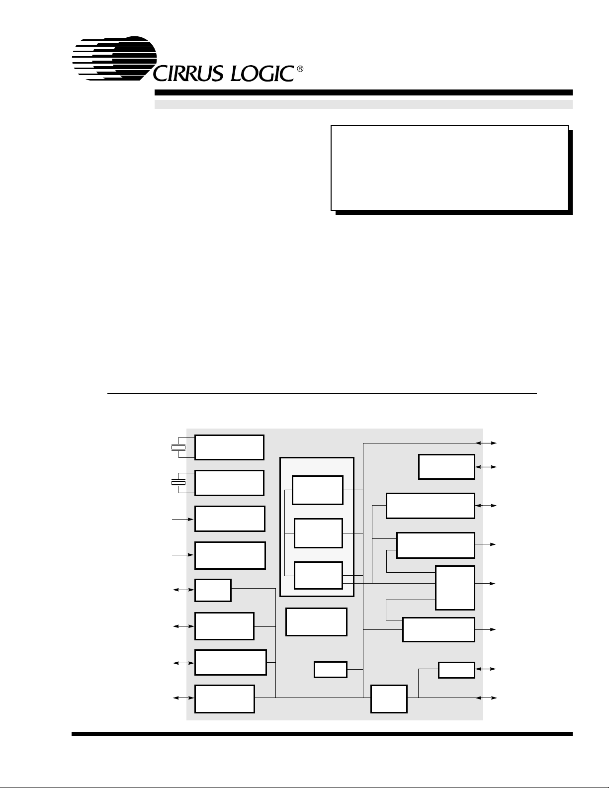
OVERVIEW
The CL-PS7110 is designed for ultra-low-power
applications such as organizers/PDAs, two-way
pagers, smart phones, and hand-held internet
browsers. The device’s core-logic functionality is
built around an ARM710A microprocessor with 8
Kbytes of four-w a y set-associativ e unified cache .
At 18.432 MHz (for 3-V operation), the CL-PS7110
delivers nearly 15 Vax-MIPS of performance (based
on Dhrystone
Low-Power
System-on-a-Chip
benchmark) — roughly the same
(cont.)
Functional Block Diagram
May 1997Version 1.5

■
■
■
■
■
■
■
■
■
■
CL-PS7110
Low-Power System-on-a-Chip
FEA TURES
(cont.)
ROM/SRAM/flash memory control
— Decodes eight separate memory segments of 256
Mbytes
— Each segment can be configured as 8, 16, or 32 bits
wide and support page-mode access
— Programmable access time for conventional
SRAM/ROM/flash memory
— Expansion device can also be a PC Card (PCMCIA)
controller
Codec interface
— Provides all necessary clocks and timing pulses and
performs serialization of the data stream (or vice versa)
to or from standard telephony codecs
— Data transfer at 64 kbps
Synchronous serial interface
— Supports SPI
1
or Microwire
2
-compatible interface
36-bit general-purpose I/O
— Four 8-bit and one 4-bit GPIO port
— Supports scanning keyboard matrix
1
SPI is a registered trademark of Motorola
2
Microwire is a registered trademark of National Semicon-
ductor
.
.
16C550-style UAR T
— Supports bit rates up to 115.2 kbps
— Contains two 16-byte FIFOs for Tx and Rx
— Supports modem control signals
SIR (slow (9600–115.2 kbps) infrared) encoder
— IrDA (Infrared Data Association) SIR protocol encoder
can be optionally switched into Tx and Rx signals of the
UART up to 115 kbps
DC-to-DC converter interface
— Provides two 96-kHz clock outputs, whose duty ratio are
programmable (from 1-in-16 to 15-in-16)
LCD controller
— Interfaces directly to a single-scan panel monochrome
LCD
— Panel size is progr ammable and is any width (line length)
from 16 to 1024 pixels in 16-pixel increments
— Video frame size programmable up to 128 Kbytes
— Bits per pixel programmable from 1, 2, or 4
— T wo 32-bit palette registers to support 4-, 2-, or 1-bit pixel
values for mapping to any of the 16 g r ayscale values
Two timer counters
Realtime clock (32-bit)
OVERVIEW
level of perf ormance offered by a 33-MHz Intel
(cont.)
’486-
based PC.
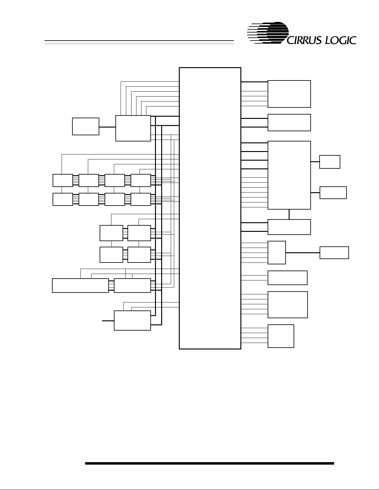
As shown in the system block diag ram, simply adding
desired memory and peripherals to the highly integrated CL-PS7110 completes a hand-held organizer/PDA system board. All the interface logic is
integrated on-chip.
The CL-PS7110 is packaged in a 208-pin VQFP
package, with a body size of 28-mm square, lead
pitch of 0.5 mm, and thickness of 1.4 mm.
Memory Interface
There are two main external memory interfaces and
a DMA controller that fetches video display data for
the LCD controller from main DRAM memory .
The SRAM/ROM-style interface has programmable
wait state timings and includes burst-mode capability ,
with eight chip selects decoding eight 256-Mbyte
sections of addressable space. For maxim um flexibility, each bank can be specified to be 8, 16 or 32 bits
wide to enable the use of low-cost memory in a 32-bit
system. The system can have an 8-bit-wide boot
option to optimize memory size.
The DRAM interface allows direct connection of up
to 4 banks of DRAM, each bank containing up to
256 Mbytes. To assure the lowest possible power
consumption, the CL-PS7110 supports self-refresh
DRAMs, which are placed a low-power state by the
device when it enters its low-pow er standb y mode.
Serial Interface
For RS232 serial communications, the CL-PS7110
includes a UAR T with two 16-byte FIFOs f or receiv e
and transmit data. The UART suppor ts bit rates of
up to 115.2 kbps. An IrDA SIR protocol
encoder/decoder can be optionally switched into the
Rx/Tx signals to/from the UAR T to enable these signals to drive an infrared communication interface
directly.
A full-duplex codec interface allows direct connection of a standard codec chip to the CL-PS7110,
allowing storage and playbac k of sound.
2
DATA BOOK v1.5
May 1997
DATA BOOK v1.5
CL-PS7110
LCD MODULE
KEYBOARD
BATTERY
DC-TO-DC
CONVERTERS
ADC
DIGITIZER
IR LED AND
PHOTODIODE
RS232
TRANSEIVER
CODEC
ADDITIONAL I/O
PCMCIA
BUFFERS
PCMCIA
SOCKET
WRITE
CS[4]
CS[5]
EXPRDY
EXPCLK
WORD
DD[3:0]
CL1
CL2
FM
M
D[31:0]
A[27:0]
COL[7:0]
PA[7:0]
DC
INPUT
NMOE
NMWE
NRAS[3]
NRAS[2]
NRAS[1]
NRAS[0]
NCAS[0]
NCAS[1]
NCAS[2]
NCAS[3]
PB[7:0]
PC[7:0]
PD[7:0]
PE[3:0]
NPOR
NPWRFL
BATOK
NEXTPWR
NBATCHG
RUN
WAKEUP
NCS[0]
NCS[1]
DRIVE[1:0]
FB[1:0]
CL-PS7110
ADCCLK
NADCCS
ADCOUT
ADCIN
SMPCLK
LEDDRV
PHDIN
RXD
TXD
DSR
CTS
DCD
PCMCK
PCMSYNC
PCMOUT
PCMIN
CS[6]
CS[7]
NCS[2]
NCS[3]
× 16
DRAM
× 16
DRAM
× 16
DRAM
× 16
DRAM
× 16
FLASH
× 16
FLASH
× 16
ROM
EXTERNAL MEMORY
MAPPED EXPANSION
BUFFERS
BUFFERS
AND
LATCHES
× 16
ROM
× 16
DRAM
× 16
DRAM
× 16
DRAM
× 16
DRAM
POWER
SUPPLY UNIT
AND
COMPARATORS
Low-Power System-on-a-Chip
A CL-PS7110–Based System
A separate synchronous serial interface supports two industry-standard protocols (SPI
and Microwire
devices such as an ADC, allo wing for peripheral
expansion such as the use of a digitizer pen.
) for interfacing to standard
Power Manag ement
The CL-PS7110 is designed for low-power
operation. There are three basic power states:
May 1997
●
Standby — This state is equivalent to the com-
puter being switched off (no display), and the
main oscillator is shut down. Only the realtime
clock is running.
●
Idle — In this state, the device is functioning and
all oscillators are running, but the processor
clock is halted while waiting for an e v ent such as
a key press.
●
Operating — This state is the same as the idle
state, except that the processor clock is running.
3

DATA BOOK v1.5
Low-Power System-on-a-Chip
TABLE OF CONTENTS
LIST OF TABLES..............................................................................................7
LIST OF FIGURES............................................................................................8
CONVENTIONS................................................................................................ 9
1. FUNCTIONAL DESCRIPTION.......................................................................11
1.1 Overview..............................................................................................................................11
1.2 General................................................................................................................................12
1.2.1 Clocking............................................................................................................................13
1.2.2 CPU Core.........................................................................................................................13
1.2.3 Interrupt Controller............................................................................................................13
1.2.4 Memory Interface and DMA..............................................................................................14
1.2.5 Expansion and Memory Controller for SRAM/ROM/Flash Interface.................................17
1.2.6 DRAM Controller ..............................................................................................................19
1.2.7 PCMCIA Support..............................................................................................................19
1.2.8 Codec Interface................................................................................................................21
1.2.9 Synchronous Serial Interface ...........................................................................................21
1.2.10 LCD Controller..................................................................................................................21
1.2.11 Internal UART and SIR Encoder.......................................................................................22
1.2.12 Timer Counters.................................................................................................................23
1.2.13 Realtime Clock .................................................................................................................23
1.2.14 DC-to-DC Converter.........................................................................................................23
1.2.15 Keyboard Control..............................................................................................................26
1.2.16 GPIO.................................................................................................................................26
1.2.17 Buzzer Control..................................................................................................................26
1.2.18 Battery Management........................................................................................................27
1.2.19 State Control.....................................................................................................................27
1.2.20 Power Management..........................................................................................................28
1.2.21 Software Model for Power Management...........................................................................29
1.2.22 Resets ..............................................................................................................................29
CL-PS7110
2. PIN INFORMATION ........................................................................................31
2.1 Pin Diagram.........................................................................................................................31
2.2 Pin Description Conventions................................................................................................32
2.3 Pin Descriptions...................................................................................................................32
2.4 Pin Descriptions...................................................................................................................35
3. PROGRAMMING INTERFACE.......................................................................39
3.1 Memory Map........................................................................................................................39
3.2 Internal Registers.................................................................................................................40
3.2.1 PADR — Port A Data Register .........................................................................................41
3.2.2 PBDR — Port B Data Register.........................................................................................41
3.2.3 PCDR — Port C Data Register.........................................................................................42
3.2.4 PDDR — Port D Data Register.........................................................................................42
3.2.5 PADDR — Port A Data Direction Register........................................................................42
3.2.6 PBDDR — Port B Data Direction Register.......................................................................42
3.2.7 PCDDR — Port C Data Direction Register.......................................................................42
3.2.8 PDDDR — Port D Data Direction Register.......................................................................42
4
TABLE OF CONTENTS
May 1997

DATA BOOK v1.5
CL-PS7110
Low-Power System-on-a-Chip
3.2.9 PEDR — Port E Data Register.........................................................................................42
3.2.10 PEDDR — Port E Data Direction Register.......................................................................42
3.2.11 SYSCON — System Control Register..............................................................................43
3.2.12 SYSFLG — System Status Flags Register ......................................................................45
3.2.13 MEMCFG1 — Memory Configuration Register 1.............................................................47
3.2.14 MEMCFG2 — Memory Configuration Register 2.............................................................47
3.2.15 DRFPR — DRAM Refresh Period Register......................................................................49
3.2.16 INTSR — Interrupt Status Register..................................................................................50
3.2.17 INTMR — Interrupt Mask Register...................................................................................52
3.2.18 LCDCON — LCD Control Register...................................................................................52
3.2.19 TC1D — Timer Counter 1 Data Register..........................................................................53
3.2.20 TC2D — Timer Counter 2 Data Register..........................................................................53
3.2.21 RTCDR — Realtime Clock Data Register........................................................................53
3.2.22 RTCMR — Realtime Clock Match Register......................................................................53
3.2.23 PMPCON — Pump Control Register................................................................................54
3.2.24 CODR — Codec Interface Data Register.........................................................................54
3.2.25 UARTDR — UART Data Register.....................................................................................55
3.2.26 UBRLCR — UART Bit Rate and Line Control Register ....................................................55
3.2.27 PALLSW Least-Significant Word-LCD Palette Register....................................................56
3.2.28 PALMSW Most-Significant Word-LCD Palette Register....................................................57
3.2.29 SYNCIO Synchronous Serial Interface Data Register......................................................58
3.2.30 STFCLR — Clear All Start Up Reason Flags Location ....................................................58
3.2.31 BLEOI — Battery Low End of Interrupt.............................................................................58
3.2.32 MCEOI — Media Changed End of Interrupt.....................................................................59
3.2.33 TEOI — Tick End of Interrupt Location.............................................................................59
3.2.34 TC1EOI TC1 — End of Interrupt Location........................................................................59
3.2.35 TC2EOI TC2 — End Of Interrupt Location.......................................................................59
3.2.36 RTCEOI — RTC Match End Of Interrupt..........................................................................59
3.2.37 UMSEOI — UART Modem Status Changed End of Interrupt...........................................59
3.2.38 COEOI — Codec End of Interrupt Location......................................................................59
3.2.39 HALT — Enter Idle State Location....................................................................................59
3.2.40 STDBY — Enter Standby State Location.........................................................................59
4. ELECTRICAL SPECIFICATIONS.................................................................. 60
4.1 Absolute Maximum Ratings.................................................................................................60
4.2 Recommended Operating Conditions..................................................................................60
4.3 DC Characteristics...............................................................................................................61
4.4 AC Characteristics...............................................................................................................62
4.5 I/O Buffer Characteristics.....................................................................................................70
4.6 Test Modes...........................................................................................................................70
4.6.1 Oscillator and PLL Bypass Mode .....................................................................................71
4.6.2 Functional (EPB) Test Mode.............................................................................................71
4.6.3 Oscillator and PLL Test Mode...........................................................................................71
4.6.4 Pin Test Mode ...................................................................................................................72
4.6.5 High-Z (System) Test Mode..............................................................................................73
4.6.6 Test ROM Mode................................................................................................................73
4.6.7 Software-Selectable Test Functionality.............................................................................74
5. PACKAGE SPECIFICA TIONS........................................................................75
5.1 208-Pin VQFP Package Outline Drawing.............................................................................75
May 1997
TABLE OF CONTENTS
5

DATA BOOK v1.5
Low-Power System-on-a-Chip
6. ORDERING INFORMATION ..........................................................................76
BIT INDEX.......................................................................................................77
INDEX..............................................................................................................79
CL-PS7110
6
TABLE OF CONTENTS
May 1997

DATA BOOK v1.5
CL-PS7110
Low-Power System-on-a-Chip
LIST OF TABLES
Table 1-1. Interrupt Allocation..................................................................................................14
Table 1-2. Physical-to-DRAM Address Mapping......................................................................19
Table 1-3. DRAM Address Mapping ........................................................................................20
Table 2-1. External Signal Functions.......................................................................................32
Table 2-2. Numeric Pin Listing.................................................................................................35
Table 3-1. Memory Map...........................................................................................................39
Table 3-2. Internal I/O Memory Locations................................................................................40
Table 3-3. Bits in SYSCON......................................................................................................43
Table 3-4. Keyboard Scan Field...............................................................................................43
Table 3-5. ADCCLK Frequencies.............................................................................................45
Table 3-6. Bits in the System Status Flags Register................................................................45
Table 3-7. Values of the Bus Width Field.................................................................................48
Table 3-8. PCMCIA Mode Bus Width.......................................................................................48
Table 3-9. Values of the Random Access Wait State Field......................................................49
Table 3-10. Values of the Sequential Access Wait State Field ..................................................49
Table 3-11. Sense of DC-to-DC Converter Control Lines..........................................................54
Table 3-12. Internal UART Bit Rates..........................................................................................56
Table 3-13. UART Word Length.................................................................................................56
Table 3-14. Least-Significant Word Palette Assignments.........................................................57
Table 3-15. Most-Significant Word Palette Assignments...........................................................57
Table 3-16. Grayscale Value to Color Mapping..........................................................................57
Table 3-17. Bits in SYNCIO Write Register................................................................................58
Table 4-1. DC Characteristics..................................................................................................61
Table 4-2. AC Characteristics..................................................................................................62
Table 4-3. I/O Buffer Output Characteristics............................................................................70
Table 4-4. CL-PS7110 Hardware Test Modes..........................................................................70
Table 4-5. EPB Test Mode Signal Assignment.........................................................................71
Table 4-6. Oscillator and PLL Test Mode Signals....................................................................72
Table 4-7. Chip Select Address Ranges During Test ROM Mode............................................73
Table 4-8. Expansion and ROM Interface Bus Width During Test ROM Mode ........................73
May 1997
LIST OF TABLES
7

DATA BOOK v1.5
Low-Power System-on-a-Chip
LIST OF FIGURES
Figure 1-1. Functional Block Diagram.......................................................................................11
Figure 1-2. Word Write to 16-bit SRAM.....................................................................................16
Figure 1-3. Word Write to 8-bit SRAM.......................................................................................17
Figure 1-4. Memory Segment Usage........................................................................................18
Figure 1-5. Video Buffer Mapping .............................................................................................22
Figure 1-6. Sample Schematic for Positive V
Figure 1-7. Sample Schematic for Negative V
Figure 1-8. State Diagram.........................................................................................................28
Figure 4-1. Expansion and ROM Read Timing..........................................................................63
Figure 4-2. Expansion and ROM Write Timing..........................................................................64
Figure 4-3. DRAM Read Cycles................................................................................................65
Figure 4-4. DRAM Write Cycles................................................................................................66
Figure 4-5. Video Quad Word Read..........................................................................................67
Figure 4-6. DRAM CAS-Before-RAS Refresh Cycle.................................................................68
Figure 4-7. LCD Controller Timing ............................................................................................69
Control Circuitry .............................................25
EE
Control Circuitry............................................26
EE
CL-PS7110
8
LIST OF FIGURES
May 1997

DATA BOOK v1.5
CL-PS7110
Low-Power System-on-a-Chip
CONVENTIONS
This following section presents conventions used in this data book.
Abbreviations and Acronyms
The following table lists abbreviations and acronyms used in this data book.
Acronym or
Abbreviation
AC alternating current
ADC analog-to-digital
codec coder/decoder
CMOS complementary metal-oxide semiconductor
CPU central processing unit
DC direct current
DMA direct-memory access
DRAM dynamic random-access memory
EPB embedded peripheral bus
FCS frame check sequence
FIFO first in/first out
GPIO general-purpose I/O
ICT in circuit test
IrDA SIR infrared data association, slow (9600–115.2 kbps) infrared
LCD liquid-crystal display
LSB least-significant bit
Definition
MIPS millions of instructions per second
MMU memory management unit
PCB printed circuit board
PDA personal digital assistant
PIA peripheral interface adapter
PLL phase locked loop
PSU power supply unit
RAM random-access memory
RISC reduced-instruction-set computer
ROM read-only memory
RTC realtime clock
SRAM static random-access memory
TLB translation look-aside buffer
May 1997
CONVENTIONS
9

DATA BOOK v1.5
CL-PS7110
Low-Power System-on-a-Chip
Acronym or
Abbreviation
UART universal asynchronous receiver transmitter
VQFP very-tight-pitch quad flat pack
Definition
Measurement Abbreviations
Symbol Units of measure
°C degree Celsius
Hz hertz (cycle per second)
Kbyte kilobyte (1,024 bytes)
kHz kilohertz
kΩ kilohm
Mbps megabits (1,048,576 bits) per second
Mbyte megabyte (1,048,576 bytes)
MHz megahertz (1,000 kilohertz)
µF microfarad
µA microampere
µs microsecond (1,000 nanoseconds)
(cont.)
mA milliampere
ms millisecond (1,000 microseconds)
ns nanosecond
V volt
W watt
OTHER CONVENTIONS
Hexadecimal numbers are presented with all letters in uppercase and a lowercase h appended. F or e xample ,
03CAh
are hexadecimal numbers.
Binary numbers are enclosed in single quotation marks when in text. F or example,
‘11’ is a
binary number.
Numbers not indicated by an h or single quotation marks are decimal.
The use of ‘tbd’ indicates values that are ‘to be determined’, ‘n/a’ designates ‘not available’, and ‘n/c’ indicates a pin
that is a ‘no connect’.
14h
and
CONVENTIONS
May 199710
DATA BOOK v1.5
CL-PS7110
32.768-kHz
OSCILLATOR
18.432-MHz
PLL
INTERRUPT
CONTROLLER
POWER
MANAGEMENT
SYNCHRONOUS
SERIAL I/O
STATE
CONTROL
DRAM
CONTROLLER
LCD
CONTROLLER
ARM7
µP CORE
8-KBYTE
CACHE
MMU
COUNTERS
(2)
RTC
CODEC
INTERFACE
ARM710A
INTERNAL DATA BUS
PSU
CONTROL
3.6864 MHz
32.786 kHz
EINT[1–3],
FIQ
BATOK, EXTPWR
PWRFL, BATCHG
PORTS A B C D — 8-BIT
PORT E — 4-BIT
KEYBOARD COLUMN
DRIVES (0–7)
BUZZER DRIVE
DC TO DC
CLK, SYNC, IN,
OUT, SMPCLK
CLK, SYNC IN,
OUT
UART
MUX
ROM/EXPANSION
CONTROL
IRDA
D0–D31
POR, RUN,
RESET,
WAKEUP
EXPCLK, WORD ,
CD[0–7], EXPRDY,
WRITE
MOE, MWE
RAS[0–3], CAS[0–3]
A[0–27],
DRA[0–12]
LCD DRIVE
LED AND PHOTODIODE
RS232 INTERFACE
INTERNAL
GPIO
ADDRESS BUS
Low-Power System-on-a-Chip
1. FUNCTIONAL DESCRIPTION
1.1 Overview
The CL-PS7110 is a single-device embedded controller designed to be used in ultra-low-cost applications
such as a hand-held personal organizers and hand-held internet browsers. There are other devices
offered by Cirrus Logic (http://www.cirrus.com) such as fax/modem chipsets, IR chipsets, codecs, etc.,
that can be used around the CL-PS7110 to build a complete hand-held organizer. The CL-PS7110 operates at both 3 V and 5 V. However, the AC timings shown in this data book (v1.5) reflect 3-V operation.
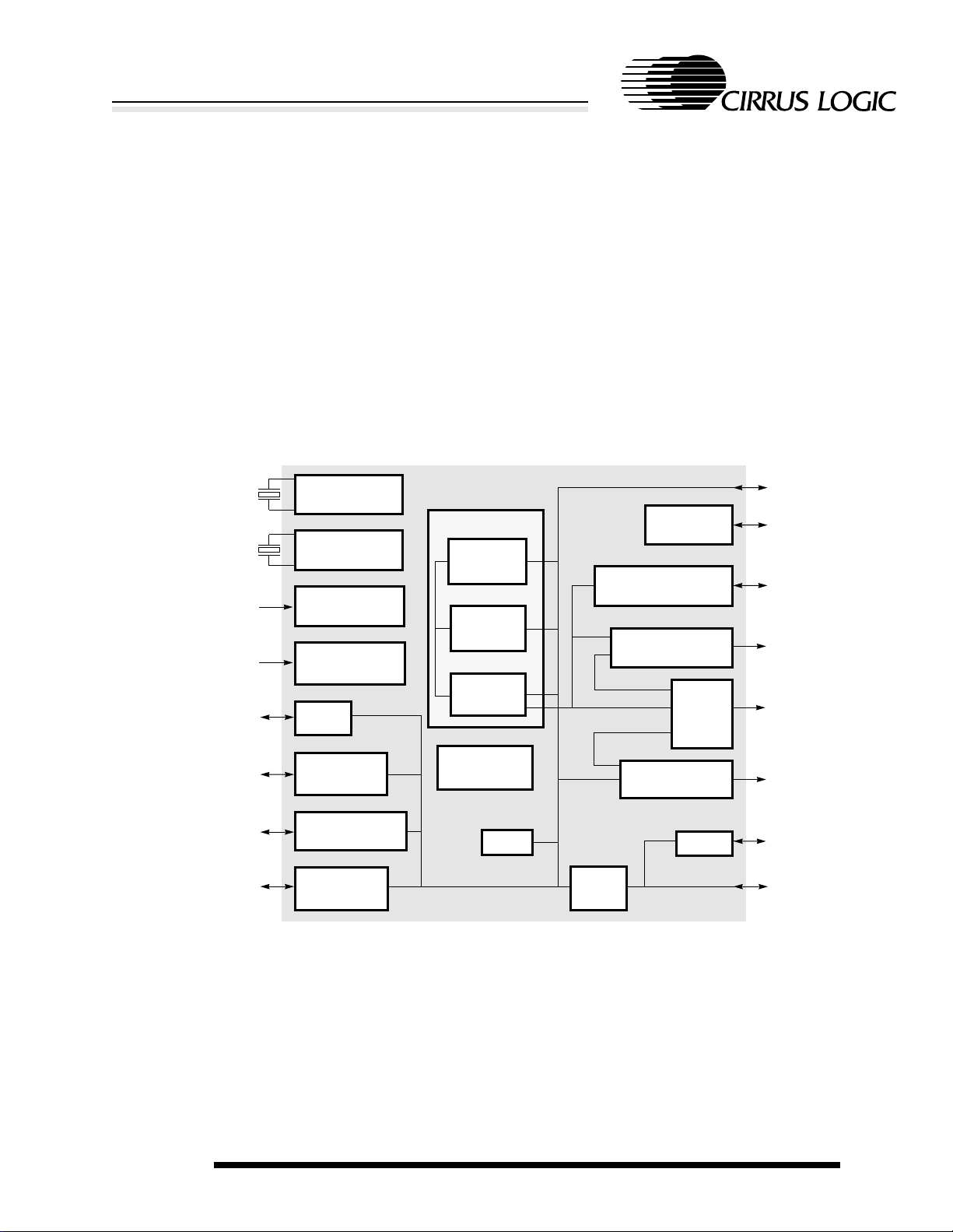
Figure 1-1 shows a simplified functional block diagram of the CL-PS7110. All external memory and
peripheral devices are connected to the 32-bit data bus, using the e xternal 28-bit address bus and control
signals. Bus transfer times can be extended using the EXPRDY signal to lengthen bus cycles. The maximum burst transfer rate of the external bus is approximately 70 Mbytes/sec.
The core-logic functionality is built around an ARM710A microprocessor and 8 Kbytes of cache. At 18.432
MHz (for 3-V operation) and with an on-chip 8-Kbyte cache (four-way set-associative), the CL-PS7110
delivers approximately 15 MIPS of sustained performance (18.4 MIPS peak). This is approximately the
same as a 33-MHz, ’486-based PC.
May 1997 11
Figure 1-1. Functional Block Diagram
FUNCTIONAL DESCRIPTION

DATA BOOK v1.5
CL-PS7110
Low-Power System-on-a-Chip
The CL-PS7110 design is optimized for low power dissipation at 3-V operation. At 18.432-MHz clock
speed, the device dissipates 66 mW during the ‘operating state’ (all oscillators and processor clock running), 15 mW in the ‘idle state’ (all oscillators running, but processor clock is halted), and 10-µW in the
‘standby state’ (no display and the main oscillator is shut down). For a definition of the three states, refer
to the Section 1.2.19 on page 27.
The CL-PS7110 can interface to up to four banks of DRAM; each bank can be up to 256 Mbytes in size.
There is also an interface for two ROMs, each up to 256 Mbytes, and six expansion devices also up to
256 Mbytes. These expansion devices could be additional ROM or a PC Card controller. The CL-PS7110
has a built-in, high-speed (115 kbps) UART with Rx and Tx FIFOs, and also supports the IrDA SIR protocol.
The CL-PS7110 is fabricated with a 0.6-µm CMOS process and is fully static. The CL-PS7110 is a 208-pin
VQFP with a body size of 28-mm square, a lead pitch of 0.5 mm, and a maximum thickness of 1.5 mm.
1.2 General
The CL-PS7110 is built around the ARM710A processor core. For a more detailed description of the
ARM710A, refer to the
CL-PS7110 are:
ARM710A Data Sheet
(http://www.arm.com/). The principle functional blocks in
● ARM710A CPU core
● Memory management unit from the ARM700 and ARM710 processors
● 8 Kbytes of unified instruction and data cache, plus a four-way set-associative cache controller
● Interrupt and fast interrupt controller
● Expansion and ROM interface giving 8 × 256-Mbyte expansion segments with independent wait state control
● DRAM controller supporting Fast Page mode and self-refresh in Standby mode
● 36 bits of general-purpose peripheral I/O
● Telephony codec interface and 16-byte FIFO
● Programmable, 4-bits-per-pixel LCD controller, mapping the video buffer into the main DRAM
● Full-duplex UART and two 16-byte FIFOs, plus logic to implement the IrDA SIR protocol, capable of speeds
up to 115 kbps
● Two 16-bit general-purpose counter timers
● A 32-bit realtime clock and comparator
● DC-to-DC converter interface
● System state control and power management
● Synchronous serial interface for Microwire
● Pin test and device-isolation logic
● External tracing support for debug
● Main oscillator and PLL (phase locked loop) to generate the system clock of 18.432 MHz from a 3.6864-MHz
or SPI peripherals (such as ADCs)
crystal
● A low-power 32.768-kHz oscillator
FUNCTIONAL DESCRIPTION
May 199712

DATA BOOK v1.5
CL-PS7110
Low-Power System-on-a-Chip
1.2.1 Clocking
The main bus clock runs at 18.432 MHz and is derived from the output of the 3.6864-MHz oscillator , using
an on-chip PLL to multiply by 10 and then divide by 2 to ensure a proper 50–50 mark space ratio is
achieved. The main bus clock is routed only to the ARM710A, the LCD controller, the memory controller
peripherals, and the baud-rate generator. Clocks required for the other per ipherals are lower frequency,
and are generally not required to be synchronous to the main bus clock. These clocks are centrally generated using ripple count stages where possible to minimize power consumption, and distributed to the
appropriate peripherals.
1.2.2 CPU Core
The ARM710A microprocessor is a 32-bit RISC processor directly connected to the 8-Kbyte unified
cache. This cache has 512 lines of four words arranged as a four-way set-associative cache. The cache
is directly connected to the ARM710A microprocessor and caches the
The MMU translates the virtual address into a physical address, it contains a 64-entry TLB (translation
look aside buffer) and is
post cache
, that is, it only translates external memory references (cache misses)
to save power.
Refer to descriptions of the Interrupt Status register (INTSR) and Internal Mask register (INTMR) in the
ARM710A Data Sheet
.
virtual address
from the processor.
1.2.3 Interrupt Controller
The ARM710A has two interrupt types: IRQ (interrupt request) and FIQ (fast interrupt request). The interrupt controller in the CL-PS7110 controls interrupts from 16 different sources. Twelve interrupt sources
are mapped to the IRQ input and four sources are mapped to the FIQ input. FIQs have a higher priority
than IRQs; if two interrupts within the same group (IRQ or FIQ) are activ e, software m ust resolve the order
in which they are serviced.
All interrupts are
1) The device asserts the appropriate interrupt request line.
2) If the appropriate bit is set in the Interrupt Mask register, either FIQ or IRQ is asserted by the interrupt con-
troller.
3) If interrupts are enabled, the processor jumps to the appropriate vector.
4) Interrupt dispatch software reads the Interrupt Status register to establish the source(s) of the interrupt, then
calls the appropriate interrupt service routine(s).
5) Software in the interrupt service routine clears the interrupt source by some action specific to the device
requesting the interrupt (for example, reading the UART Rx register).
6) The interrupt service routine can then re-enable interrupts, any other pending interrupts are serviced in a similar way or returned to the interrupt dispatch code, which checks for any more pending interrupts and dispatches them accordingly.
level-sensitive,
that is, they must conform to the following sequence.
May 1997 13
FUNCTIONAL DESCRIPTION

DATA BOOK v1.5
Table 1-1. Interrupt Allocation
CL-PS7110
Low-Power System-on-a-Chip
Interrupt
FIQ 0 EXTFIQ External fast interrupt input (NEXTFIQ pin).
FIQ 1 BLINT Battery low interrupt.
FIQ 2 WEINT Watch dog expired interrupt.
FIQ 3 MCINT Media changed interrupt.
IRQ 4 CSINT Codec sound interrupt.
IRQ 5 EINT1 External interrupt input 1 (NEINT1 pin).
IRQ 6 EINT2 External interrupt input 2 (NEINT2 pin).
IRQ 7 EINT3 External interrupt input 3 (EINT3 pin).
IRQ 8 TC1OI TC1 under flow interrupt.
IRQ 9 TC2OI TC2 under flow interrupt.
IRQ 10 RTCMI RTC compare match interrupt.
IRQ 11 TINT 64-Hz tick interrupt.
IRQ 12 UTXINT Internal UART transmit FIFO empty interrupt.
IRQ 13 URXINT Internal UART receive FIFO full interrupt.
Bit in Mask
and ISR
Name Comment
IRQ 14 UMSINT Internal UART modem status changed interrupt.
IRQ 15 SSEOTI Synchronous serial interface end of transfer interrupt.
1.2.4 Memory Interface and DMA
The CL-PS7110 memory controller is designed for maximum flexibility. Requests for external memory
accesses from the ARM710A are decoded and the appropriate external memory access or inter nal bus
cycle is initiated accordingly.
There are two main external memory interfaces:
● DRAM controller
● Expansion memory controller for SRAM/FLASH/ROM
The CL-PS7110 provides a DMA controller (see Section 1.2.5) that allows video displa y data f or the LCD
controller to be fetched directly from main DRAM memory, independent of internal CL-PS7110 activity.
Bus cycles generated by the CL-PS7110 depend on the requester and the target. The possible requesters
are the ARM710A core, the DMA controller and the DRAM refresh controller . The two types of targets are
DRAM banks and ROM/expansion banks . A data transf er ma y tak e multiple bus cycles . The arbitration for
the bus is at the beginning of a transfer. The priority is fixed with DMA highest, then refresh, followed by
the ARM710A. Once granted the bus, the maximum burst to a ROM/expansion bank is four bus cycles,
regardless of the transfer width. The ARM710A core can produce byte , word, m ulti-w ord accesses. Multi-
FUNCTIONAL DESCRIPTION
May 199714

DATA BOOK v1.5
CL-PS7110
Low-Power System-on-a-Chip
word accesses are produced by cache line fetches and b loc k data tr ansf er instructions. They can be considered a burst of word reads.
Reads
For byte reads , the CL-PS7110 will rotate the data if needed so that, regardless of the width of the memory bank, the addressed byte is in the correct position. The remaining bytes will be filled with zeros. Normally, word accesses to non-word aligned addresses cause an alignment fault. However, if the alignment
fault check in the MMU is not enabled, a word read from an address offset from a word boundary will
cause the data to be rotated into the register as if it were a byte read. Half-word aligned reads will place
the data in correct bytes of the register. Two shift operations are then required to zero-fill or sign extend
the data.
Writes
During byte writes, the data is replicated on each of the four bytes of the data b us. F or DRAM writes, there
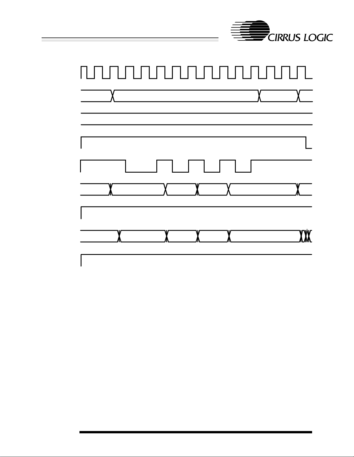
is CAS line per byte and only the CAS for the correct b yte is enabled. For writes to byte-wide ROM/e xpansion banks, the nMWE signal is directly used as the write enable. For writable 16-bit ROM/expansion
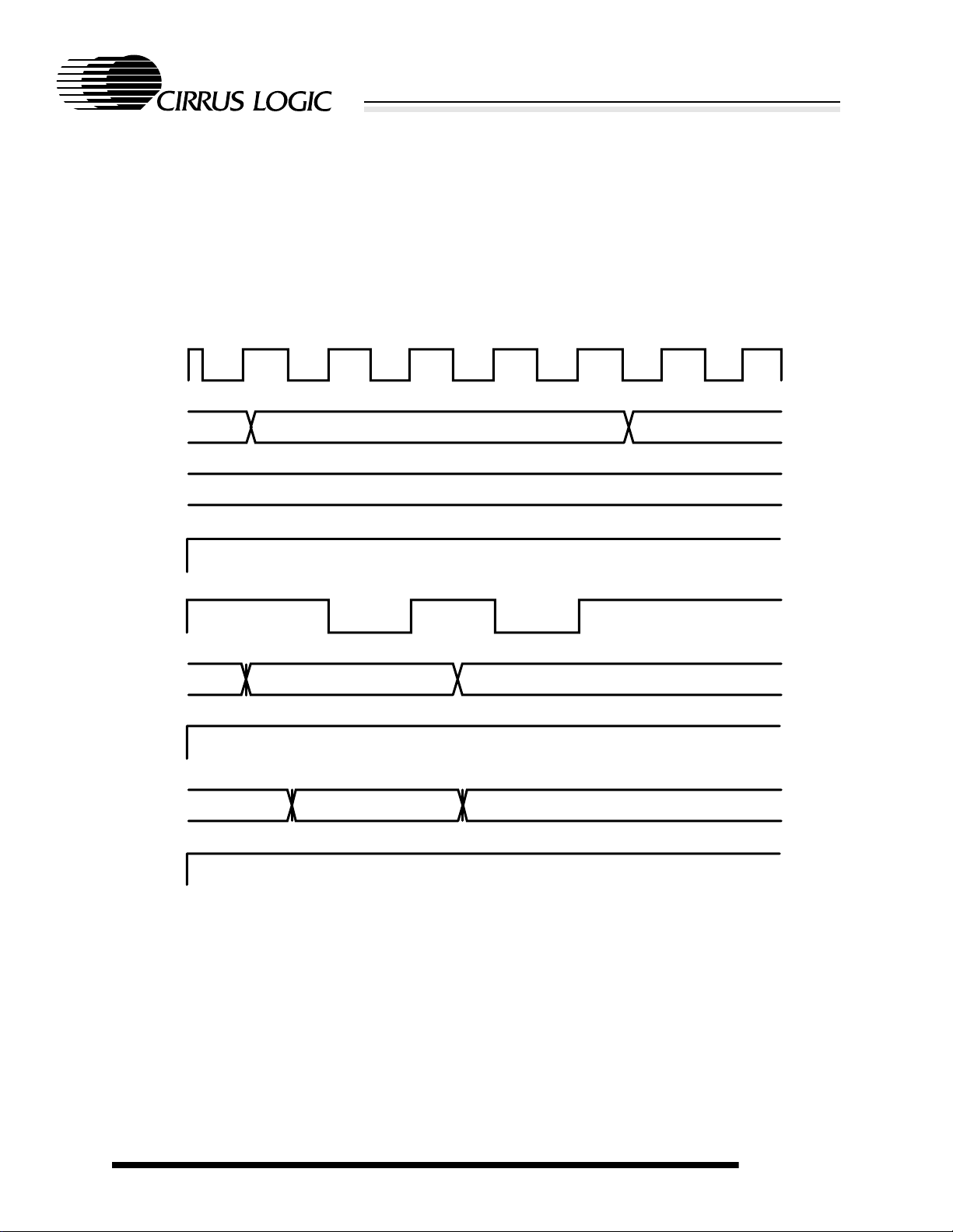
banks, two write enables must be decoded from the WORD, nMWE and address line A0 (refer to
Figure 1-2). F or writable 32-bit ROM/e xpansion banks, f our write enables must be decoded from the same
signals plus the A1 address line. A byte write always causes a single bus cycle. Word writes to wordaligned addresses are handled by the CL-PS7110, regardless of the width of the ROM/expansion bank.
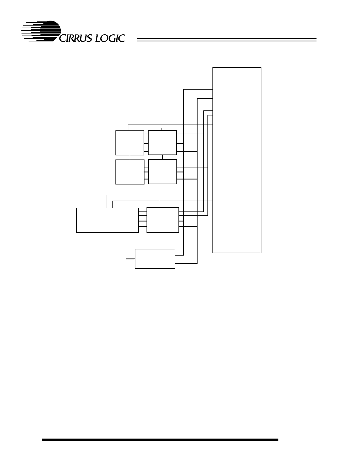
Accesses to 8- or 16-bit-wide banks will cause multiple bus cycles (refer to Figure 1-3). Word wr ites to
non-word-aligned addresses normally cause a alignment fault. If the alignment fault check in the MMU is
not enabled, non-aligned work writes act as if both low address bits were zero.
May 1997 15
FUNCTIONAL DESCRIPTION
DATA BOOK v1.5
CL-PS7110
EXPCLK
NCS
CS
NMWE
A
WORD
D
EXPRDY
1111 1101 1111
0000
0000144 0000000 0000002
XXXXXXXX XXXX4567 XXXX0123
NMOE
Low-Power System-on-a-Chip
NOTE: A store of 0X01234567 is split into two 16-bit stores by CL-PS7110 hardware.
Figure 1-2. Word Write to 16-bit SRAM
FUNCTIONAL DESCRIPTION
May 199716
DATA BOOK v1.5
CL-PS7110
EXPCLK
NCS
CS
NMWE
A
WORD
EXPRDY
1111 1011 1111 1110
0000
000021C 0000000 0000001 0000002 0000003 0000220
XXXXXXXX XXXXXX67 XXXXXX45 XXXXXX23 XXXXXX01
D
NMOE
Low-Power System-on-a-Chip
NOTE: A store of 0X0123456 is split into four 8-bit stores by CL-PS7110 hardware.
1.2.5 Expansion and Memory Controller for SRAM/ROM/Flash Interface
Figure 1-3. Word Write to 8-bit SRAM
Eight separate linear memory or expansion segments are decoded by the CL-PS7110. Each segment is
256 Mbytes in size and can be interf aced by using a conv entional SRAM-like interf ace. Each segment can
be individually programmed to be 8, 16, or 32 bits wide, support Page mode access, and execute from
0–4 wait states. In addition, bus cycles can be extended using the EXPRDY input signal. Two segments
are allocated to ROM program segments and six to memory-mapped expansion. How ev er, this is arbitr ary
and can be redefined. Page mode access is accomplished by running up to four accesses together, this
can significantly improve bus bandwidth to devices, such as ROMs. Sequential Burst mode access is
always faulted (the bus returned to idle) after four
refresh cycles.
accesses,
regardless of bus width to allow DMA and
Each memory area has a single byte control register field, allowing the bus width and access timing to be
programmed. Refer to the description of MEMCFG1 and MEMCFG2 registers on page 47.
May 1997 17
FUNCTIONAL DESCRIPTION
DATA BOOK v1.5
Figure 1-4 shows the usage of such memory segments.
CL-PS7110
D[0:31]
A[0:27]
× 16
FLASH
× 16
ROM
× 16
FLASH
× 16
ROM
EXTERNAL MEMORY
MAPPED EXPANSION
BUFFERS
BUFFERS
AND
LATCHES
NMOE
NMWE
NCS0
NCS1
CS6
CS7
NCS2
NCS3
ADDITIONAL I/O
CL-PS7110
Low-Power System-on-a-Chip
Figure 1-4. Memory Segment Usage
The width of each the ROM/expansion bank is set in its Memory Configuration Register 1 (see
Section 3.2.13). This register is cleared to zero by a power-on reset. The CL-PS7110 boots from
ROM/expansion bank 0. To allow for booting from 8- or 32-bit memory devices, the state of port E bit 0 is
sampled during power-on reset and stored into the BOOT8BIT Mode register. If this bit is low, all zeros in
the width field of a memory configuration register indicates a 32-bit-wide bank and all ones a 8-bit device.
If this bit is high, the decoding of the bus width field is inverted, so all zeros indicates a 8-bit device.This
way, a pull-up or pull-down on port E bit 0 indicates the size of the boot device. For consistency, the
BOOT8BIT Mode has the same effect on all ROM/expansion banks.
The PCMCIA mode is a special case. If the width field of the Memor y Configuration Register 1 is set to
PCMCIA mode, the upper address bits are decoded to determine the bus width and type of access. The
PCMCIA address bits A0 to A25 are driven by CL-PS7110 address bits A0 to A25. CL-PS7110 address
bits A26 and A27 are decoded to specify the type and width of the access. If both are zeros, it is an access
to the 8-bit-wide attribute memory . If only A26 is a one, it is an access to the 16-bit-wide common memory.
If only A27 is a one, it is an access to a 8-bit-wide I/O register . If both are ones, it is an access to a 16-bitwide I/O register.
The ARM710A core only supports byte or word accesses. Normally , w ord accesses are conv erted to multiple bus cycles that match the width of the ROM/e xpansion bank. Word accesses to PCMCIA 16-bit-wide
FUNCTIONAL DESCRIPTION
May 199718

DATA BOOK v1.5
CL-PS7110
Low-Power System-on-a-Chip
I/O registers are the exception. Reading or writing an I/O register may have side effects, so a single 16bit access is needed. A byte access may trigger a side effect before the other byte is transferred, and a
word access could affect neighboring I/O registers. To provide 16-bit-wide accesses, no bus width conversion is done for w ord accesses. Instead, there is a single bus cycle with only data bits D0 to D15 valid.
If alignment fault checking is enabled in the ARM710A core, all word accesses require a word-aligned
address, that is both A0 and A1 must be zero. To access the 16-bit I/O registers that are not at wordaligned addresses (that is, A1 is one), the CL-PS7110 makes special use of address bit 25. F or a PCMCIA
bank, if address bits A25 to A27 are all ones, the A25 output pin is driven low and the A1 output pin is
driven high.This restricts 16-bit accesses to the low 32 Mbytes of the PCMCIA I/O space, but allows
access to all registers in this range.
1.2.6 DRAM Controller
The DRAM controller in the CL-PS7110 provides all connections to directly interface up to four banks of
DRAM. Each bank is 32-bits wide and up to 256 Mbytes in size. Four RAS lines are provided, one per
bank and four CAS lines are provided, one per byte line. As the DRAM device size is not programmable,
if devices are used that are smaller than the largest size supported (1 Gbit) this leads to a segmented
memory map, each bank being separated by 256 Mbytes. Segments that are smaller than the bank size
repeat within the bank. Table 1-2 shows the mapping of physical address to DRAM row and column
address. This mapping has been organized to support any DRAM device size from 4 Mbit to 1 Gbit with
a ‘square’ row and column configuration, that is, the number of column addresses is equal to the n umber
of row addresses. If a non-square DRAM is used, fur ther fragmentation of the memory map can occur ;
however, the smallest contiguous segment is always 1 Mbyte.
In addition to supporting standard refresh cycles, self-refresh DRAM is suppor ted such that system
DRAM can be put into a low-power state by the ARM710A before entering its low-power Standby mode.
DMA takes priority over other external memory or I/O accesses under the control of the internal bus arbiter. Requests for more data are received from the FIFO b uff er at the front end of the datapath through the
LCD controller. The DMA request is serviced by providing a quad word of data from the frame buffer that
starts at location zero in main DRAM memory. Meanwhile the CPU continues execution, including
accesses to the other peripherals. Ref er to Section 1.2.10 on page 21 for the description of the LCD controller.
1.2.7 PCMCIA Support
As mentioned in Section 1.2.5 (expansion memory controller), there are eight separate linear memory
segments supported and one can use one of the segments to interface with a PCMCIA card.
To design a PCMCIA-card interface to support 3/5-V cards and hot insertion, isolation buffers for address
and data will be required. A sample design is provided in CL-PS7110 Evaluation kit. A PAL (22LV10) is
used to decode PCMCIA card signals out of the CL-PS7110 address and control bus. The PAL equations
are available in the
Evaluation Kit User’s Manual
.
Table 1-2. Physical-to-DRAM Address Mapping
Memory
Address
0 A2 A10 A27/DRA0
DRAM
Column
DRAM Row Pin Name
1 A3 A11 A26/DRA1
May 1997 19
FUNCTIONAL DESCRIPTION

DATA BOOK v1.5
CL-PS7110
Low-Power System-on-a-Chip
Table 1-2. Physical-to-DRAM Address Mapping
2 A4 A12 A25/DRA2
3 A5 A13 A24/DRA3
4 A6 A14 A23/DRA4
5 A7 A15 A22/DRA5
6 A8 A16 A21/DRA6
7 A9 A17 A20/DRA7
8 A19 A18 A19/DRA8
9 A21 A20 A18/DRA9
10 A23 A22 A17/DRA10
11 A25 A24 A16/DRA11
12 A27 A26 A15/DRA12
(cont.)
Table 1-3 shows the address mapping for various DRAMs with square and non-square row and address
inputs assuming two ×16 devices are connected to each RAS line. This mapping is then repeated every
256 Mbytes for each DRAM bank.
n
is given by n = 0xC + bank number (for example, 0xC for bank 0;
0xF for bank 3, etc.).
Table 1-3. DRAM Address Mapping
Device
Size
4 Mbits 9 Row × 9 Column 1 Mbyte n000.0000–n00F.FFFF 1 Mbyte
16 Mbits 10 Row × 10 Column 4 Mbytes n000.0000–n03F.FFFF 4 Mbytes
16 Mbits 12 Row × 8 Column 4 Mbytes
64 Mbits 11 Row × 11 Column 16 Mbytes n000.0000–n0FF.FFFF 16 Mbytes
64 Mbits 13 Row × 9 Column 16 Mbytes
Address
Configuration
Total Size
of Bank
Address Range of
Segment(s)
n000.0000– n007.FFFF
n010.0000–n017.FFFF
n040.0000–n047.FFFF
n050.0000–n057.FFFF
n100.0000–n107.FFFF
n110.0000–n117.FFFF
n140.0000–n147.FFFF
n150.0000–n157.FFFF
n000.0000–n01F.FFFF
n040.0000–n05F.FFFF
n100.0000–n11F.FFFF
n140.0000–n15F.FFFF
n400.0000–n41F.FFFF
n440.0000–n45F.FFFF
n500.0000–n51F.FFFF
n540.0000–n55F.FFFF
Size of
Segment(s)
512 Kbytes
2 Mbytes
256 Mbits 12 Row × 12 Column 64 Mbytes n000.0000–n3FF.FFFF 64 Mbytes
1 Gbit 13 Row × 13 Column 256 Mbytes n000.0000–nFFF.FFFF 256 Mbytes
FUNCTIONAL DESCRIPTION
May 199720

DATA BOOK v1.5
CL-PS7110
Low-Power System-on-a-Chip
The DRAM controller contains a programmable refresh counter. The refresh rate is controlled using the
DRAM Refresh Period register (DRFPR).
1.2.8 Codec Interface
The codec interface allows a direct connection of a telephony-type codec to the CL-PS7110. It provides
all the necessary clocks and timing pulses and performs serialization of the data stream (or vice versa)
to or from the codec. The interface is full-duplex and contains two separate data FIFOs.
Data is transferred to or from the codec at 64 kbps, either written to or read from the appropriate 16-byte
FIFO. The sound interrupt is generated ev ery 8 bytes transferred (FIFO half full/empty), which means the
interrupt rate is reduced from 8 to 1 kHz with a latency of 1 ms.
1.2.9 Synchronous Serial Interface
The synchronous serial interface allows peripheral devices , such as ADCs, that ha ve a SPI- or Micro wirecompatible interface to be directly connected to the CL-PS7110. The clock output frequency (ADCCLK)
is programmable and only active dur ing data transmissions to save power (refer to the Example 1 table
on page 24). The output channel is fed by an 8-bit shift register, and the input channel is captured by a
16-bit shift register. The clock and synchronization pulses are activated by a write to the Output Shift register. During transfers the SSIBUSY (Synchronous Serial Interface Busy) bit in the System Status Flags
register is set. When the transfer is complete and valid data is in the 16-bit read shift register the SSEOTI
interrupt is asserted and the SSIBUSY bit is cleared. An additional sample clock (SMPCLK) can be
enabled independently and is set at twice the transfer clock frequency.
1.2.10 LCD Controller
The LCD controller provides all necessary control signals to directly interface to a single-scan panel multiplexed LCD. The panel size is programmable and can be any width (line length) from 16 to 1024 pixels
in 16-pixel increments. The total video frame size is programmable up to 128 Kbytes. This equates to a
theoretical maximum panel size of 1024 × 256 pixels in 4-bits-per-pixel mode. The LCD controller uses a
9-stage FIFO to buffer the incoming displa y data, which is replenished by hardware DMA under the control
of the CL-PS7110 DMA controller.
The video RAM is mapped into the base of the main DRAM memory area, which is fixed at physical
address 0xC000.0000. The number of bits per pixel is programmable from 1, 2, or 4.
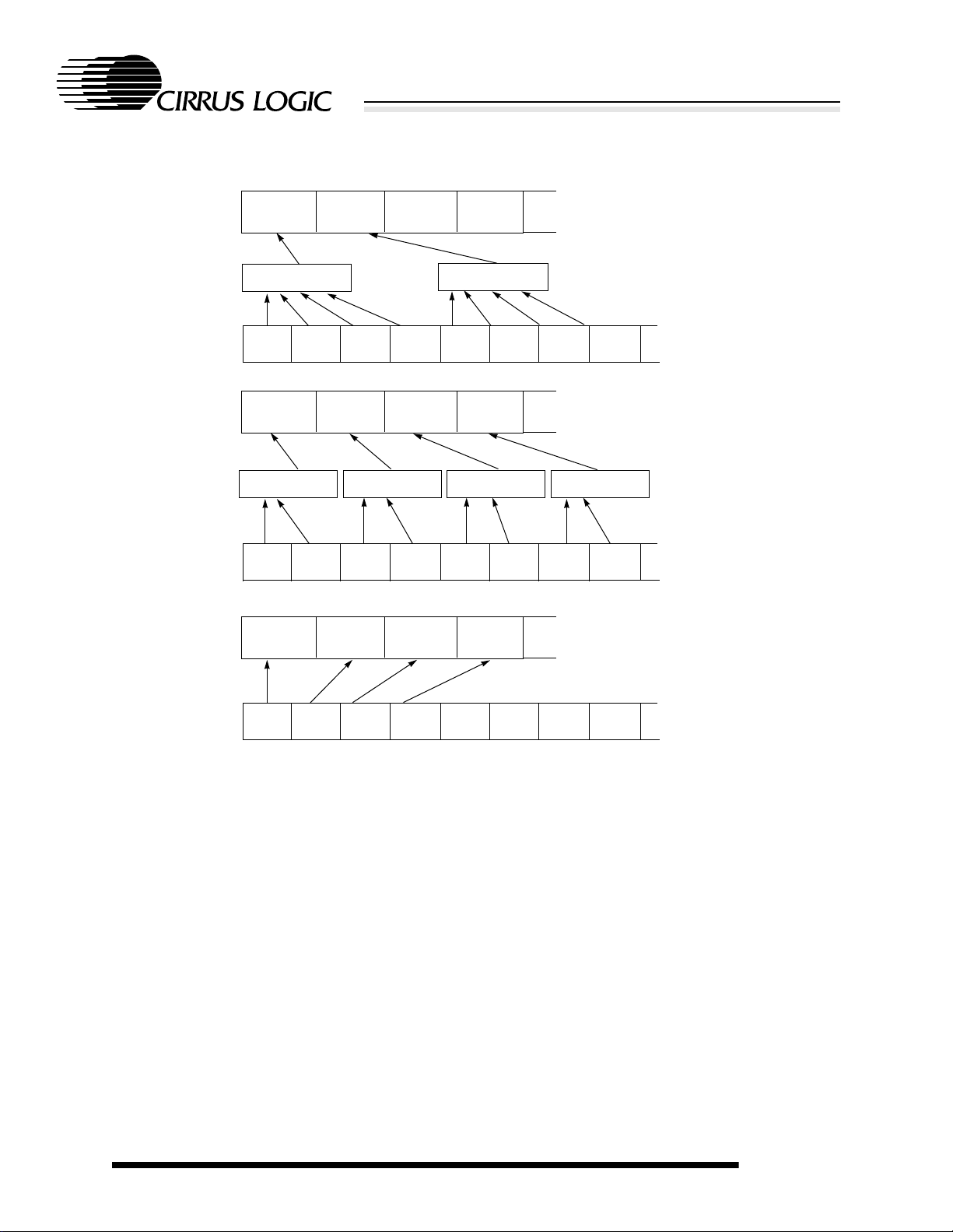
The screen is mapped to the video buffer as one contiguous block where each horizontal line of pixels is
mapped to a set of consecutive bytes or words in the video RAM. The video b uffer can be accessed w ordwide as pixel 0 is mapped to the LSB in the buff er , that is, the pix els are arranged in a little-endian manner .
The pixel bit rate and the LCD refresh rate can be programmed from 18.432 MHz to 576 kHz. The LCD
controller is programmed by writing to the LCD Control register (LCDCON).
The LCD controller also contains two 32-bit palette registers, these allow any 4-, 2-, or 1-bit pixel value to
be mapped to any of the 15 grayscale values available. Any 4-bit logical grayscale value can be mapped
to any of the 16 physical grayscales. The palettes are written to directly as two 32-bit memory-mapped
registers.
Figure 1-5 on page 22 shows the organization of the video map for all combinations of bits per pixel.
May 1997 21
FUNCTIONAL DESCRIPTION
DATA BOOK v1.5
CL-PS7110
BIT 0 BIT 1 BIT 2 BIT 3 BIT 4 BIT 5 BIT 6 BIT 7
PIXEL 1 PIXEL 2 PIXEL 3 PIXEL 4
GRAYSCALE
GRAYSCALE
GRAYSCALE GRAYSCALE GRAYSCALE GRAYSCALE
2 BITS PER PIXEL
4 BITS PER PIXEL
1 BIT PER PIXEL
PIXEL 1 PIXEL 2 PIXEL 3 PIXEL 4
BIT 0 BIT 1 BIT 2 BIT 3 BIT 4 BIT 5 BIT 6 BIT 7
PIXEL 1 PIXEL 2 PIXEL 3 PIXEL 4
BIT 0 BIT 1 BIT 2 BIT 3 BIT 4 BIT 5 BIT 6 BIT 7
Low-Power System-on-a-Chip
Figure 1-5. Video Buffer Mapping
The refresh rate is not affected by the n umber of bits per pixel. Howe ver, the LCD controller fetches twice
the data per refresh for 4-bits-per-pixel compared to 2-bits-per-pixel. The main reason for reducing the
number of bits per pixel is to reduce the power consumption of the DRAMs in bank 0 where the video
buffer is mapped.
1.2.11 Internal UART and SIR Encoder
The CL-PS7110 contains a built-in UART, which offers similar functionality to the National Semiconduc-
tor
16C550 device. It can support bit rates of up to 115.2 kbps and contains two 16-byte FIFOs for
receive and transmit.
Only three modem-control input signals are supported: CTS, DSR, and DCD. The additional RI input
modem control line is not supported. Output modem control lines (such as, R TS and DTR) are not e xplicitly supported, but can be implemented using bits from the general-purpose PIA ports in the CL-PS7110.
FUNCTIONAL DESCRIPTION
May 199722

DATA BOOK v1.5
CL-PS7110
Low-Power System-on-a-Chip
UAR T operation and line speed are controlled by the U AR T Bit Rate and Line Control (UBRLCR) register .
Three interrupts can be generated by the UART: Rx, Tx, and Modem Status Changed. The Rx interrupt
is asserted when the FIFO becomes half full or if the FIFO is non-empty for longer than three character
length times with no more characters being received. The Tx interrupt is asser ted if the FIFO buffer
reaches half empty. The Modem Status Changed interrupt is generated if either of the modem status bits
change state.
Framing and parity errors are detected as each byte is receiv ed and pushed onto the Rx FIFO . An ov errun
error generates an Rx interrupt immediately. All error bits can be read from the 11-bit-wide data register.
The FIFO can also be programmed to only be 1 byte deep (such as, a conventional UART with double
buffering).
The CL-PS7110 also contains an IrDA SIR protocol encoder . This encoder can be optionally s witched into
the Tx and Rx signals , so that these can be used to directly drive an infr ared interface. If the SIR protocol
encoder is enabled, the UART Tx line is held in the passive state and transitions of the Modem Status
Changed or Rx lines have no effect.
1.2.12 Timer Counters
The CL-PS7110 has two integrated identical timer counters, referred to as TC1 and TC2. Each timer
counter has an associated 16-bit read/write data register and some control bits in the System Control register. Each counter is immediately loaded with the v alue written to the data register . This value is then
remented
on the second active clock edge to arrive after the write (that is, after the fist complete period
of the clock). When the timer counter under-flows (reaches 0) the appropriate interrupt is asserted. The
timer counters can be read at any time. The clock source and mode are selectable by writing to various
bits in the System Control register (clock sources are 512 and 2 kHz).
dec-
The timer counters can operate in two modes: Free-running or Prescale.
1.2.12.1 Free-Running Mode
In Free-running mode, the counter wraps around to 0xFFFF when it under-flows and continues counting
down. Any value written to TC1 or TC2 is decremented on the second edge of the selected clock.
1.2.12.2 Prescale Mode
In Prescale mode, the value written to TC1 or TC2 is automatically reloaded when the counter underflows. Any value written to TC1 or TC2 is decremented on the second edge of the selected clock. This
mode can produce a programmable frequency to drive the buzzer or generate a periodic interrupt.
1.2.13 Realtime Clock
The CL-PS7110 contains a 32-bit RTC (realtime clock). The RTC can be wr itten to and read from in the
same manner as the timer counters, but is 32 bits wide. The R TC is alw a ys cloc k ed at 1 Hz and also contains a 32-bit output-match register, which can be programmed to generate an interrupt when the time in
the RTC matches a specific time written to this register.
1.2.14 DC-to-DC Converter
Two programmable duty ratio 96-kHz clock outputs are provided by the CL-PS7110. These drives are to
be used as DC-to-DC converters in the PSU (power-supply unit) subsystem. These clocks are enabled
by external input pins that are normally connected to the output from comparators monitoring the DC-toDC converter output. The duty ratio (and hence the converter on-time) can be programmed from 1-in-16
May 1997 23
FUNCTIONAL DESCRIPTION

DATA BOOK v1.5
CL-PS7110
Low-Power System-on-a-Chip
to 15-in-16. The sense of the DC-to-DC converter drive signal (active-high or -low) is determined by latching the state of this drive signal during power-on reset (that is, a pull-up resistor on the drive signal results
in an active-low drive output and vice versa). This allo ws either positive or negative voltages to be generated by the DC-to-DC converter.
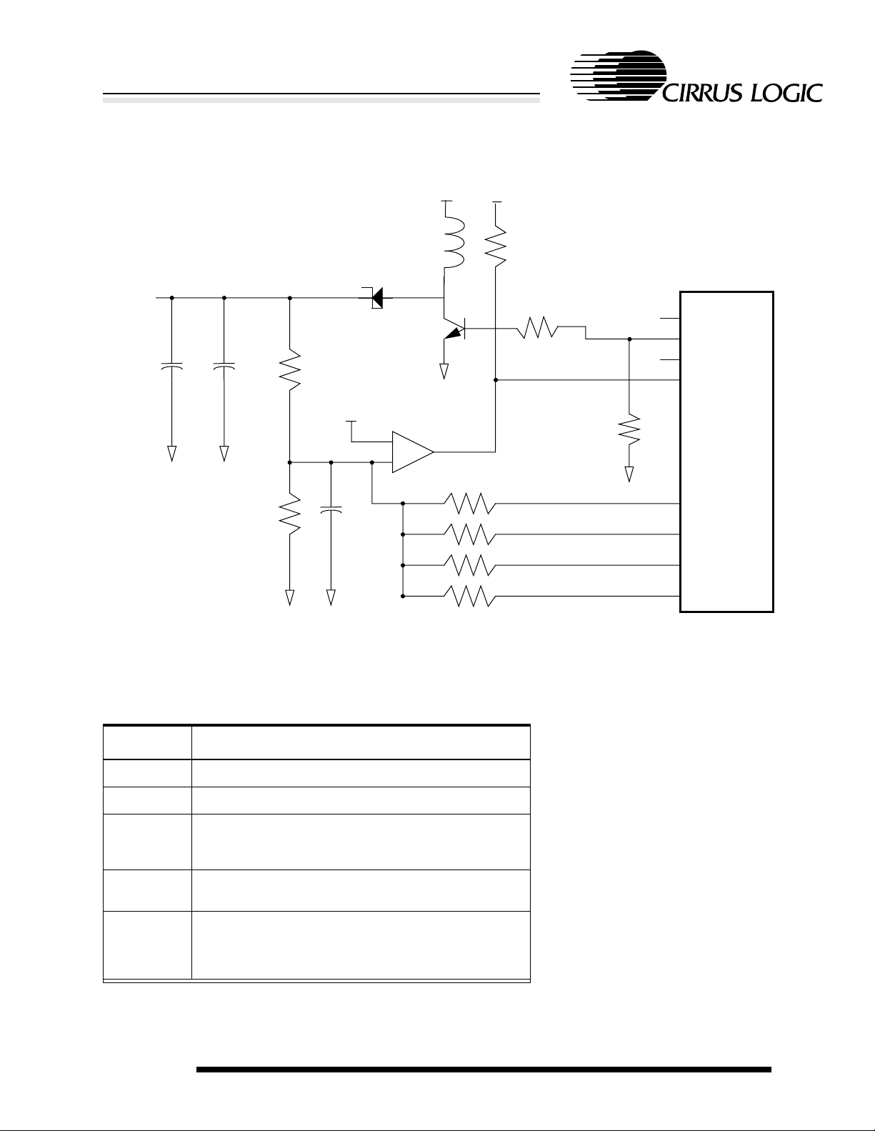
An example of how to use the DC-to-DC con v erter is shown below. The objective of Example 1 is to have
constant V
as PD4, PD5, PD6 and PD7 in Figure 1-2 and Figure 1-3) are used to choose various resistor values. The
Drive 1 pin is connected to the base of the biasing transistor. The V
required.The feedback mechanism via the FB1 pin ensures that whenever software changes the pulse
width using the Pump Control register (PMPCON), the voltage level is kept at the desired level for V
for the bias generator of an LCD panel to control the contrast. Four of the GPIO pins (shown
EE
is the maximum voltage that is
EE
EE
.
The same technique could be used for keeping V
for flash at a constant level as shown in Example 2.
PP
Example 1
Following is a sample schematic for a positive and negative VEE control circuitry. The same circuitry may
be applied for the 12-V V
generator. Assume that the nominal VEE voltage for a given LCD is 28 V, and
PP
the range covered is from 27 to 29 V (to assure a sufficient contrast control range).
Resistor Notes
R75 Pull down for positive VEE.
R53 Pull up for LM339 open-drain output.
R54
R55
R62–65
1. Connect a load resistor over C2 to force approximately 2 mA of current (or whate ver your panel’s typical
value is).
Choose to select a voltage at the + terminal of the comparator at what point the feedback output will switch off
(high), thus turning off the Drive output.
To select voltage level on the + input of the comparator to
application V
This resistor network allows V
under program control. If all outputs are low, V
maximum. Turning on the outputs increases the voltage
at the comparator, and therefore decreases V
REF
(1.5V).
to be programmed
EE
is at the
EE
.
EE
2. Program the Pump Control register to 5, set PD7..4 to high.
3. Set R55 such that VEE is at the minimum 27 V.
4. Set PC7..4 to ‘1111’; VEE should exceed 29 V.
FUNCTIONAL DESCRIPTION
May 199724
DATA BOOK v1.5
CL-PS7110
+V
EE
C2
2.2
µ 10 µF
GND
GND
GND
GND
GND
C78
R54
330 k
V
REF
LM339
FB0
DRIVE0
R74
UI3A
DRIVE1
FB1
GND
82
81
87
86
100 k
R75
V
DD
100 k
R53
U19
V
DD
L3
47
µH
R55
R
100 n
806 k
C44
R64
R65
R63
R62
392 k
200 k
100 k
64
PD4
PD5
PD6
PD7
63
62
61
CL-PS7110
FB1
4
5
3
2
3
2
1
4
D12
1N5818
100 k
DRIVE1
-
+
Low-Power System-on-a-Chip
Now the panel can be connected and the contrast fine-tuned by changing the Pump Control register v alue
for the appropriate drive output.
Figure 1-6. Sample Schematic for Positive V
Control Circuitry
EE
Example 2
(1.5 V).
Resistor Notes
R73 Pull down for positive VEE.
R53 Pull up for LM339 open-drain output.
R54
R56
R62–65
Selects a voltage at the terminal of the comparator, at
which point the feedback output switches off (high), thus
turning off the Drive output.
Selects voltage level on input of comparator to application V
REF
This resistor network allows V
under program control. If all outputs are low, V
maximum. Turning on the outputs increases the voltage
at the comparator, and therefore decreases V
May 1997 25
to be programmed
EE
is at the
EE
.
EE
FUNCTIONAL DESCRIPTION
 Loading...