

Cirrus Logic CL-GD5446 (64-bit VisualMedia Accelerator) GD5446 Technical Reference Manual Nov 1996

CL-GD5446 Extended Display Modes Summary
Mode
No.
58, 6A 102 16/256K 800 × 600 100 × 37 56, 60, 72, 75
5C 103 256/256K 800 × 600 100 × 37 56, 60, 72, 75, 85
5D 104 16/256K 1024 × 768 128 × 48 43i
5E 100 256/256K 640 × 400 80 × 25 70
5F 101 256/256K 640 × 480 80 × 30 60, 72, 75, 85
60 105 256/256K 1024 × 768 128 × 48 43i, 60, 70, 72, 75, 85
64 111 64K 640 × 480 – 60, 72, 75, 85
65 114 64K 800 × 600 – 56, 60, 72, 75, 85
66 110 32K 640 × 480 – 60, 72, 75, 85
67 113 32K 800 × 600 – 56, 60, 72, 75, 85
68 116 32K 1024 × 768 – 43i, 60, 70, 75, 85
69 119 32K 1280 × 1024 – 43i, 60
6C 106 16/256K 1280 × 1024 160 × 64 43i
6D 107 256/256K 1280 × 1024 160 × 64 43i, 60, 75
71 112 16M 640 × 480 – 60, 72, 75, 85
74 117 64K 1024 × 768 – 43i, 60, 70, 75, 85
VESA
No.
Colors
Display
Resolution
Chars. Refresh (Hz)
a
, 60, 70, 72, 75
75 11A 64K 1280 × 1024 – 43i
78 115 16M 800 × 600 – 56, 60, 72, 75, 85
79 118 16M 1024 × 768 – 43i, 60, 70, 75, 85
7B – 256/256K 1600 × 1200 – 48i
7C – 256/256K 1152 × 864 – 70, 75
a. ‘i’ indicates interlaced.
Refer to Table 3-2, “Cirrus Logic Extended Display Modes,” on page 3-25.

CL-GD5446
Technical Reference Manual
November 1996
Second Edition

Notice
Cirrus Logic Inc. has made best efforts to ensure that the information contained in this document
is accurate and reliable. However, the information is subject to change without notice. No
responsibility is assumed by Cirrus Logic Inc. for the use of this information, nor for infringements
of patents or other rights of third parties. Cirrus, Cirrus Logic, AccuPak, DIVA, FastP ath, FasText,
FeatureChips, Good Data, Laguna, Laguna3D, MediaDAC, MotionVideo, SimulSCAN, S/LA,
SMASH, SofTarget, TextureJet, TVTap, UXART, VisualMedia, VPM, V-Port, Voyager, WavePort,
and WebSet are trademarks of Cirrus Logic Inc., which may be registered in some
jurisdictions. Other trademarks in this document belong to their respective companies. CR US and
Cirrus Logic International, Ltd. are trade names of Cirrus Logic Inc.
Copyright Notice
This document is the property of Cirrus Logic Inc. and implies no license under patents, copyrights, or trade secrets. No part of this publication may be copied, reproduced, stored in a retrie v al
system, or transmitted, in any form or by an y means, electronic, mechanical, photog raphic, or otherwise, or used as the basis for manufacture or sale of any items without the prior written consent
of Cirrus Logic Inc.
Copyright
1995, 1996— Cirrus Logic, Inc. All rights reserved.

Contents

CONTENTS
The following are the differences between the December 1995 and November 1996 versions of
this technical reference manual:
●
CL-GD5446 Technical Reference Manual
Revision History
Information pertaining to the Revision B device has been added
November 1996 ii Copyright 1996 – Cirrus Logic Inc.

CL-GD5446 Technical Reference Manual
CONTENTS
Table of Contents
1. INTRODUCTION ..................................................................................... 1-2
1.1 Scope of Document............................................................................................. 1-2
1.2 Chip Types Covered............................................................................................ 1-2
1.3 Intended Audience .............................................................................................. 1-2
1.4 Conventions ........................................................................................................ 1-2
2. OVERVIEW ............................................................................................. 2-2
2.1 Features.............................................................................................................. 2-2
2.2 Major Components.............................................................................................. 2-4
2.3 VGA Core............................................................................................................ 2-4
2.4 PCI Bus Interface.............................................................................................. 2-12
2.5 BitBLT Engine ................................................................................................... 2-12
2.6 Video Capture ................................................................................................... 2-13
2.7 Video Window and Video Display ..................................................................... 2-13
2.8 Hardware/Software Compatibility...................................................................... 2-14
2.9 Computer Display Subsystem Architecture....................................................... 2-14
3. DATA BOOK ........................................................................................... 3-1
4. VGA CORE REGISTERS ....................................................................... 4-2
4.1 POS94: POS102 Access Control........................................................................ 4-5
4.2 POS102: POS102............................................................................................... 4-6
4.3 VSSM: 3C3 (Planar) Sleep Address ................................................................... 4-7
4.4 VSSM: 46E8 (Adapter) Sleep Address ............................................................... 4-8
4.5 MISC: Miscellaneous Output............................................................................... 4-9
4.6 FC: Feature Control........................................................................................... 4-11
4.7 FEAT: Input Status Register 0........................................................................... 4-12
4.8 STAT: Input Status Register 1........................................................................... 4-13
4.9 Pixel Mask......................................................................................................... 4-14
4.10 Palette Address (Read Mode, Write only)........................................................ 4-15
4.11 DAC State (Read only)..................................................................................... 4-16
4.12 Palette Address (Write Mode).......................................................................... 4-17
4.13 Palette Data....................................................................................................... 4-18
4.14 SRX: Sequencer Index...................................................................................... 4-19
4.15 SR0: Sequencer Reset...................................................................................... 4-20
4.16 SR1: Sequencer Clocking Mode....................................................................... 4-21
4.17 SR2: Sequencer Plane Mask............................................................................ 4-22
4.18 SR3: Sequencer Character Map Select............................................................ 4-23
4.19 SR4: Sequencer Memory Mode........................................................................ 4-25
4.20 CRX: CRTC Index............................................................................................. 4-26
4.21 CR0: CRTC Horizontal Total............................................................................. 4-29
Copyright 1996 – Cirrus Logic Inc. iii November 1996

CONTENTS
4.22 CR1: CRTC Horizontal Display End.................................................................. 4-30
4.23 CR2: CRTC Horizontal Blanking Start............................................................... 4-31
4.24 CR3: CRTC Horizontal Blanking End................................................................ 4-32
4.25 CR4: CRTC Horizontal Sync Start .................................................................... 4-34
4.26 CR5: CRTC Horizontal Sync End...................................................................... 4-35
4.27 CR6: CRTC Vertical Total................................................................................. 4-37
4.28 CR7: CRTC Overflow........................................................................................ 4-38
4.29 CR8: CRTC Screen A Preset Row-Scan .......................................................... 4-39
4.30 CR9: CRTC Character Cell Height.................................................................... 4-40
4.31 CRA: CRTC Text Cursor Start .......................................................................... 4-41
4.32 CRB: CRTC Text Cursor End............................................................................ 4-42
4.33 CRC: CRTC Screen Start Address High........................................................... 4-43
4.34 CRD: CRTC Screen Start Address Low............................................................ 4-44
4.35 CRE: CRTC Text Cursor Location High............................................................ 4-45
4.36 CRF: CRTC Text Cursor Location Low............................................................. 4-46
4.37 CR10: CRTC Vertical Sync Start....................................................................... 4-47
4.38 CR11: CRTC Vertical Sync End........................................................................ 4-48
4.39 CR12: CRTC Vertical Display End.................................................................... 4-50
4.40 CR13: CRTC Offset (Pitch)............................................................................... 4-51
4.41 CR14: CRTC Underline Row Scanline.............................................................. 4-52
4.42 CR15: CRTC Vertical Blank Start...................................................................... 4-53
4.43 CR16: CRTC Vertical Blank End....................................................................... 4-54
4.44 CR17: CRTC Mode Control............................................................................... 4-55
4.45 CR18: CRTC Line Compare.............................................................................. 4-57
4.46 CR22: Graphics Data Latches Readback (Read only)..................................... 4-58
4.47 CR24: Attribute Controller Toggle Readback (Read only) ............................... 4-59
4.48 CR26: Attribute Controller Index Readback (Read only).................................. 4-60
4.49 GRX: Graphics Controller Index........................................................................ 4-61
4.50 GR0: Set/Reset / Background Color Byte 0...................................................... 4-62
4.51 GR1: Set/Reset Enable / Foreground Color Byte 0........................................... 4-63
4.52 GR2: Color Compare......................................................................................... 4-64
4.53 GR3: Data Rotate.............................................................................................. 4-65
4.54 GR4: Read Map Select ..................................................................................... 4-66
4.55 GR5: Graphics Controller Mode........................................................................ 4-67
4.56 GR6: Miscellaneous.......................................................................................... 4-69
4.57 GR7: Color Don’t Care...................................................................................... 4-70
4.58 GR8: Bit Mask................................................................................................... 4-71
4.59 ARX: Attribute Controller Index......................................................................... 4-72
4.60 AR0–ARF: Attribute Controller Palette.............................................................. 4-73
4.61 AR10: Attribute Controller Mode ....................................................................... 4-74
4.62 AR11: Overscan (Border) Color........................................................................ 4-76
4.63 AR12: Color Plane Enable ................................................................................ 4-77
CL-GD5446 Technical Reference Manual
November 1996 iv Copyright 1996 – Cirrus Logic Inc.

CL-GD5446 Technical Reference Manual
4.64 AR13: Pixel Panning ......................................................................................... 4-78
4.65 AR14: Color Select............................................................................................ 4-79
CONTENTS
5. BITBLT EXTENSION REGISTERS ........................................................ 5-2
5.1 GR10–GR15: Color Expansion Foreground/Background Colors........................ 5-3
5.2 GR20–GR21: BLT Width Byte 0, 1...................................................................... 5-4
5.3 GR22–GR23: BLT Height Byte 0, 1 .................................................................... 5-5
5.4 GR24–GR25: BLT Destination Pitch Byte 0, 1.................................................... 5-6
5.5 GR26–GR27: BLT Source Pitch Byte 0, 1 .......................................................... 5-7
5.6 GR28–GR2A: BLT Destination Start Byte 0, 1, 2................................................ 5-8
5.7 GR2C–GR2E: BLT Source Start Byte 0, 1, 2...................................................... 5-9
5.8 GR2F: BLT Destination Left-Side Clipping........................................................ 5-10
5.9 GR30: BLT Mode .............................................................................................. 5-11
5.10 GR31: BLT Start/Status..................................................................................... 5-13
5.11 GR32: BLT ROP (Raster Operation)................................................................. 5-15
5.12 GR33: BLT Mode Extensions............................................................................ 5-17
5.13 GR34–GR35: Transparent BLT Key Color Byte 0, 1......................................... 5-18
6. VIDEO CAPTURE AND PLAYBACK REGISTERS ............................... 6-2
6.1 CR31: Video Window Horizontal Zoom Control.................................................. 6-4
6.2 CR32: Video Window Vertical Zoom Control ...................................................... 6-5
6.3 CR33: Video Window Horizontal Region 1 Size.................................................. 6-6
6.4 CR34: Video Window Region 2 Width................................................................. 6-7
6.5 CR35: Video Window Region 2 Source Data Size.............................................. 6-8
6.6 CR36: Video Window Horizontal Overflow.......................................................... 6-9
6.7 CR37: Video Window Vertical Start................................................................... 6-10
6.8 CR38: Video Window Vertical End.................................................................... 6-11
6.9 CR39: Video Window Vertical Overflow............................................................ 6-12
6.10 CR3A–CR3B: Video Buffer 1 Start Address Byte 0, 1 ...................................... 6-13
6.11 CR3C: Video Buffer 1 Start Address Byte 2...................................................... 6-14
6.12 CR3D: Video Buffer Address Offset.................................................................. 6-15
6.13 CR3E: Video Window Master Control............................................................... 6-16
6.14 CR3F: Miscellaneous Video Control ................................................................. 6-18
6.15 CR50: Video Capture Control............................................................................ 6-20
6.16 CR51: Video Capture Data Format................................................................... 6-22
6.17 CR52: Video Capture Horizontal Data Reduction............................................. 6-23
6.18 CR53: Video Capture Vertical Data Reduction ................................................. 6-24
6.19 CR54: Video Capture Horizontal Delay............................................................. 6-25
6.20 CR56: Video Capture Vertical Delay................................................................. 6-26
6.21 CR57: Video Capture Maximum Height............................................................ 6-27
6.22 CR58: Video Capture Miscellaneous Control.................................................... 6-28
6.23 CR59–CR5A: Video Buffer 2 Start Address Byte 0, 1....................................... 6-29
6.24 CR5B: Video Window Brightness Adjust........................................................... 6-30
Copyright 1996 – Cirrus Logic Inc. v November 1996

CONTENTS
6.25 CR5C: Luminance-Only Capture Control.......................................................... 6-31
6.26 CR5D: Video Window Pixel Alignment.............................................................. 6-32
6.27 CR5E: Double-Buffer Control............................................................................ 6-33
6.28 GR1C–GR1F: Chroma Key............................................................................... 6-35
CL-GD5446 Technical Reference Manual
7. PCI CONFIGURATION REGISTERS ..................................................... 7-2
7.1 PCI00: PCI Device/Vendor ID............................................................................. 7-3
7.2 PCI04: PCI Status/Command.............................................................................. 7-4
7.3 PCI08: PCI Class Code....................................................................................... 7-5
7.4 PCI10: PCI Display Memory Base Address........................................................ 7-6
7.5 PCI14: PCI Relocatable I/O / GPIO Base Address (Revision A)......................... 7-7
7.6 PCI14: PCI VGA/BitBLT Register Base Address (Revision B)............................ 7-8
7.7 PCI18: PCI GPIO Base Address (Revision B).................................................... 7-9
7.8 PCI2C: PCI Subsystem/Subsystem Vendor ID (Revision B) ............................ 7-10
7.9 PCI30: PCI Expansion ROM Base Address Enable.......................................... 7-11
7.10 PCI3C: PCI Interrupt ......................................................................................... 7-12
8. MISCELLANEOUS EXTENSION REGISTERS ..................................... 8-2
8.1 SR6: Key............................................................................................................. 8-4
8.2 SR7: Extended Sequencer Mode........................................................................ 8-5
8.3 SR8: DDC2B/EEPROM Control.......................................................................... 8-7
8.4 SR9–SRA: Scratch Pad 0, 1............................................................................... 8-9
8.5 SRB–SRE: VCLK0–VCLK3 Numerator............................................................. 8-10
8.6 SRF: DRAM Control.......................................................................................... 8-11
8.7 SR10: Graphics Cursor X Position.................................................................... 8-13
8.8 SR11: Graphics Cursor Y Position.................................................................... 8-14
8.9 SR12: Graphics Cursor Attribute....................................................................... 8-15
8.10 SR13: Graphics Cursor Pattern Address Offset................................................ 8-16
8.11 SR14–SR15: Scratch Pad 2, 3.......................................................................... 8-17
8.12 SR16: Display FIFO Threshold Control............................................................. 8-18
8.13 SR17: Configuration Readback and Extended Control..................................... 8-19
8.14 SR18: Signature Generator Control.................................................................. 8-20
8.15 SR19: Signature Generator Result Low-Byte.................................................... 8-22
8.16 SR1A: Signature Generator Result High-Byte .................................................. 8-23
8.17 SR1B–SR1E: VCLK0–VCLK3 Denominator and Post-Scalar........................... 8-24
8.18 SR1F: MCLK Select.......................................................................................... 8-25
8.19 GR9: Offset Register 0...................................................................................... 8-26
8.20 GRA: Offset Register 1...................................................................................... 8-28
8.21 GRB: Graphics Controller Mode Extensions..................................................... 8-29
8.22 GRC: Color Key/Chroma Key Compare............................................................ 8-31
8.23 GRD: Color Key/Mask/Chroma Key.................................................................. 8-32
8.24 GRE: Power Management ................................................................................ 8-33
8.25 GR16: Active Display Line Readback Byte 0.................................................... 8-35
November 1996 vi Copyright 1996 – Cirrus Logic Inc.

CL-GD5446 Technical Reference Manual
8.26 GR17: Active Display Line Readback Byte 1.................................................... 8-36
8.27 GR18: Extended DRAM Controls...................................................................... 8-37
8.28 GR19: GPIO Port Configuration........................................................................ 8-39
8.29 GR1A–GR1B: Scratch Pad 4, 5........................................................................ 8-40
8.30 CR19: Interlace End.......................................................................................... 8-41
8.31 CR1A: Miscellaneous Control ........................................................................... 8-42
8.32 CR1B: Extended Display Controls .................................................................... 8-44
8.33 CR1C: Sync Adjust and GENLOCK.................................................................. 8-46
8.34 CR1D: Overlay Extended Control ..................................................................... 8-48
8.35 CR25: Part Status (Read only).......................................................................... 8-50
8.36 CR27: ID (Read only)........................................................................................ 8-51
8.37 HDR: Hidden DAC Register.............................................................................. 8-52
CONTENTS
9. PROGRAMMING NOTES ....................................................................... 9-2
9.1 Introduction.......................................................................................................... 9-2
9.2 Resource Addressing.......................................................................................... 9-2
9.3 Pixel Addressing and Formats .......................................................................... 9-11
9.4 BitBLT Engine ................................................................................................... 9-18
9.5 Video Window ................................................................................................... 9-31
9.6 Video Capture ................................................................................................... 9-41
9.7 Overlay: CL-GD543X/’4X Compatibility............................................................. 9-47
9.8 Hardware Cursor............................................................................................... 9-53
9.9 Frequency Synthesizer Programming............................................................... 9-54
9.10 Power Management.......................................................................................... 9-57
9.11 CRTC Programming.......................................................................................... 9-58
9.12 Chip Identification.............................................................................................. 9-61
9.13 CL-GD5446 Interrupt System............................................................................ 9-61
9.14 Programming Examples.................................................................................... 9-62
10. DETAILED PIN DESCRIPTIONS ......................................................... 10-2
10.1 Host Interface: PCI Bus..................................................................................... 10-2
10.2 Video Interface.................................................................................................. 10-4
10.3 Display Memory Interface.................................................................................. 10-6
10.4 General-Purpose I/O......................................................................................... 10-7
10.5 V-Port
10.6 Miscellaneous Pins............................................................................................ 10-8
10.7 Clock Synthesizer.............................................................................................. 10-8
10.8 Power and Ground............................................................................................ 10-9
............................................................................................................. 10-7
11. ELECTRICAL SPECIFICATIONS ........................................................ 11-2
11.1 Absolute Maximum Ratings............................................................................... 11-2
11.2 DC Specifications (Digital)................................................................................. 11-3
11.3 DAC Characteristics.......................................................................................... 11-4
11.4 AC Specifications.............................................................................................. 11-5
Copyright 1996 – Cirrus Logic Inc. vii November 1996

CONTENTS
CL-GD5446 Technical Reference Manual
APPENDIXES
A1 CONNECTOR PINOUTS ......................................................................A1-2
A2 REVISION B NOTES ............................................................................A2-2
1. INTRODUCTION .............................................................................................. A2-2
2. DESIGN CHANGES .........................................................................................A2-2
2.1 PCI10 Claims 32 Mbytes....................................................................... A2-2
2.2 PCI14 Supports VGA and BitBLT Registers......................................... A2-2
2.3 PCI18 Supports GPIO........................................................................... A2-2
2.4 PCI2C Supports Subsystem and Subsystem Vendor ID ...................... A2-2
2.5 General-Purpose I/O Configuration....................................................... A2-3
B1 LAYOUT GUIDELINES .........................................................................B1-2
1. INTRODUCTION .............................................................................................. B1-2
2. PARTS PLACEMENT AND ADAPTER CARDS ..............................................B1-2
2.1 PCI Bus Adapter Card........................................................................... B1-2
2.2 Motherboard.......................................................................................... B1-3
3. POWER ............................................................................................................ B1-3
4. GROUND ......................................................................................................... B1-4
5. DECOUPLING CAPACITORS .........................................................................B1-5
6. SYNTHESIZER ................................................................................................B1-6
7. IREF CIRCUITRY ............................................................................................. B1-6
8. RGB LINES ...................................................................................................... B1-6
9. DRAM ARRAY ................................................................................................. B1-6
B2 PCI BUS REFERENCE DESIGN ..........................................................B2-2
1. INTRODUCTION .............................................................................................. B2-2
2. PCI BUS INTERFACE ...................................................................................... B2-2
2.1 Bus Connections................................................................................... B2-2
2.2 INTR# Pin............................................................................................. B2-3
2.3 VGA BIOS............................................................................................. B2-3
3. DISPLAY MEMORY INTERFACE .................................................................... B2-3
3.1 Memory Configurations......................................................................... B2-3
3.2 Damping Resistors................................................................................ B2-3
4. MONITOR INTERFACE ................................................................................... B2-4
4.1 RGB Lines............................................................................................. B2-4
4.2 Sync Lines............................................................................................. B2-4
4.3 Monitor ID.............................................................................................. B2-4
5. FEATURE CONNECTOR ................................................................................ B2-5
6. VMI HOST PORT ............................................................................................. B2-6
7. POWER DISTRIBUTION AND CONDITIONING ............................................. B2-8
7.1 Introduction ........................................................................................... B2-8
7.2 Dedicated Ground Plane....................................................................... B2-8
7.3 Dedicated Power Plane......................................................................... B2-8
November 1996 viii Copyright 1996 – Cirrus Logic Inc.

CL-GD5446 Technical Reference Manual
7.4 Power Bypassing.................................................................................. B2-8
7.5 Analog Power Conditioning................................................................... B2-9
8. CONFIGURATION RESISTORS ..................................................................... B2-9
9. DUAL-FREQUENCY SYNTHESIZERS SUPPORT ....................................... B2-10
9.1 Synthesizer Reference........................................................................ B2-10
9.2 Synthesizer Filters.............................................................................. B2-10
10. DAC CURRENT REFERENCE ...................................................................... B2-10
11. PCI BUS SCHEMATICS ................................................................................ B2-10
CONTENTS
B3 MEMORY CONFIGURATIONS AND TIMING ......................................B3-2
1. INTRODUCTION .............................................................................................. B3-2
2. DRAM CONFIGURATIONS ............................................................................. B3-2
3. CL-GD5440/’46 DUAL LAYOUT CONSIDERATIONS ..................................... B3-3
4. DRAM CONNECTION TABLES .......................................................................B3-3
5. DRAM TIMING REQUIREMENTS ...................................................................B3-7
5.1 Extended RAS# Timing......................................................................... B3-7
5.2 EDO Timing.......................................................................................... B3-7
5.3 DRAM Timing Equations Evaluated...................................................... B3-8
6. MCLK vs. DISPLAY MODE REQUIREMENTS ..............................................B3-11
7. BANDWIDTH NOTE FOR CL-GD5440 WITH 64-BIT INTERFACE .............. B3-12
B4 CURRENT REFERENCE ......................................................................B4-2
1. INTRODUCTION .............................................................................................. B4-2
2. RSet: FULL-SCALE CURRENT SET RESISTOR VALUE ...............................B4-2
B5 CONFIGURATION NOTES ...................................................................B5-2
1. INTRODUCTION .............................................................................................. B5-2
2. CONFIGURATION SUMMARY ........................................................................ B5-2
3. CONFIGURATION DETAILS ........................................................................... B5-3
B6 SIGNATURE GENERATOR .................................................................B6-2
1. INTRODUCTION .............................................................................................. B6-2
2. TESTING .......................................................................................................... B6-2
B7 PIN SCAN .............................................................................................B7-2
1. INTRODUCTION .............................................................................................. B7-2
2. TEST METHOD ................................................................................................ B7-2
2.1 Entering Pin-Scan Mode....................................................................... B7-2
2.2 Exiting Pin-Scan Mode.......................................................................... B7-2
3. PIN SCAN ORDER .......................................................................................... B7-2
B8 DDC2B/I
1. INTRODUCTION .............................................................................................. B8-2
2
C SUPPORT ..........................................................................B8-2
B9 GENLOCK SUPPORT ..........................................................................B9-2
1. INTRODUCTION .............................................................................................. B9-2
2. GENLOCK ON THE CL-GD5446 ..................................................................... B9-2
3. VSYNC GENLOCK PROGRAMMING ............................................................. B9-3
4. HSYNC GENLOCK PROGRAMMING .............................................................B9-3
Copyright 1996 – Cirrus Logic Inc. ix November 1996

CONTENTS
CL-GD5446 Technical Reference Manual
B10MANUFACTURING TEST ..................................................................B10-2
1. INTRODUCTION ............................................................................................B10-2
2. OPERATING INSTRUCTIONS ......................................................................B10-2
3. INSTALLING AND STARTING MFGTST .......................................................B10-2
3.1 Command Line Options...................................................................... B10-3
4. USING MFGTST ............................................................................................B10-4
4.1 Special Keystrokes.............................................................................. B10-4
5. UPDATES ......................................................................................................B10-6
B11GENERAL-PURPOSE I/O ..................................................................B11-2
1. INTRODUCTION ............................................................................................B11-2
2. GPIO CONFIGURATION ...............................................................................B11-2
3. PINS REDEFINED .........................................................................................B11-3
4. CYCLE TIMING CONTROL ...........................................................................B11-4
5. GPIO PROGRAMMING EXAMPLE ...............................................................B11-7
C1 SOFTWARE SUPPORT .......................................................................C1-2
1. INTRODUCTION ..............................................................................................C1-2
2. CL-GD5446 VGA SOFTWARE UTILITIES ......................................................C1-2
2.1 CLMODE — A Display Mode Configuration Utility................................ C1-2
2.2 VGA.EXE — RAMBIOS Utility.............................................................. C1-2
2.3 OEMSI
2.4 WINMODE Utility................................................................................... C1-3
3. CL-GD5446 VGA SOFTWARE DRIVERS .......................................................C1-4
3.1 Driver Applicability................................................................................. C1-4
(OEM System Integration) Utility.............................................. C1-3
C2 VGA BIOS .............................................................................................C2-2
1. BIOS OVERVIEW ............................................................................................C2-2
1.1 Main BIOS Features.............................................................................. C2-2
1.2 Extended Display Mode Support........................................................... C2-2
1.3 Direct-Color Operation.......................................................................... C2-2
1.4 High Performance................................................................................. C2-2
1.5 System Integration................................................................................ C2-3
1.6 Customization....................................................................................... C2-3
1.7 Compatibility.......................................................................................... C2-3
2. CL-GD5446 VGA BIOS INITIALIZATION .........................................................C2-3
3. VIDEO BIOS INTERRUPT VECTORS .............................................................C2-5
4. INTERRUPT 10h: INDEX .................................................................................C2-6
5. DESCRIPTION OF FUNCTIONS .....................................................................C2-8
5.1 Function 00h: Set Display Mode.............................................. C2-8
5.2 Function 01h: Set Cursor Type................................................ C2-9
5.3 Function 02h: Set Cursor Position......................................... C2-10
5.4 Function 03h: Get Cursor Position......................................... C2-10
November 1996 x Copyright 1996 – Cirrus Logic Inc.

CL-GD5446 Technical Reference Manual
5.5 Function 04h: Get Light Pen Position
(no longer supported) .........................................................................C2-11
5.6 Function 05h: Select Active Display Page.......................................... C2-11
5.7 Function 06h: Window Scroll Up......................................................... C2-11
5.8 Function 07h: Window Scroll Down.................................................... C2-12
5.9 Function 08h: Read Character/Attribute at Cursor Position................ C2-12
5.10 Function 09h: Write Character/Attribute at Cursor Position................ C2-13
5.11 Function 0Ah: Write Character at Cursor Position.............................. C2-14
5.12 Function 0Bh, Subfunction 00h: Set Background/Border Color.......... C2-14
5.13 Function 0Bh, Subfunction 01h: Select Palette Set............................ C2-15
5.14 Function 0Ch: Write Dot (Pixel) .......................................................... C2-15
5.15 Function 0Dh: Read Dot (Pixel).......................................................... C2-15
5.16 Function 0Eh: Write Character to Active RAM in Teletype Mode....... C2-16
5.17 Function 0Fh: Get Display State......................................................... C2-16
5.18 Function 10h, Subfunction 00h: Set Individual Palette Register
(Internal Palette Register) ...................................................................C2-16
5.19 Function 10h, Subfunction 01h: Set Overscan (Border)
Register ..............................................................................................C2-17
5.20 Function 10h, Subfunction 02h: Set All Palette Registers and
OverScan Register .............................................................................C2-17
5.21 Function 10h, Subfunction 03h: Toggle Intensify/Blinking Bit............. C2-17
5.22 Function 10h, Subfunction 07h: Read Individual Palette Register
(Internal Palette Register) ...................................................................C2-18
5.23 Function 10h, Subfunction 08h: Read OverScan (Border) Register... C2-18
5.24 Function 10h, Subfunction 09h: Read All Palette Registers and OverScan
Register ..............................................................................................C2-18
5.25 Function 10h, Subfunction 10h: Set Individual Color Register
(RAMDAC/External Palette Registers) ...............................................C2-18
5.26 Function 10h, Subfunction 12h: Set Block of Color Registers............ C2-19
5.27 Function 10h, Subfunction 13h: Select Color Page
(Not valid in Mode 13h) .......................................................................C2-19
5.28 Function 10h, Subfunction 15h: Read Individual Color Register
(RAMDAC/External Palette Registers) ...............................................C2-20
5.29 Function 10h, Subfunction 17h: Read Block of Color Registers......... C2-20
5.30 Function 10h, Subfunction 1Ah: Read Current State of Color Page
(Not valid in Mode 13h) .......................................................................C2-21
5.31 Function 10h, Subfunction 1Bh: Sum Color Values to
Grayshades ........................................................................................C2-21
5.32 Function 11h, Subfunction 00h: Load User Text Font ........................ C2-21
5.33 Function 11h, Subfunction 01h: Load 8 × 14 ROM Font..................... C2-22
5.34 Function 11h, Subfunction 02h: Load 8 × 8 ROM Font....................... C2-23
5.35 Function 11h, Subfunction 03h: Select Block Specifier ...................... C2-24
5.36 Function 11h, Subfunction 04h: Load 8 × 16 ROM Font..................... C2-25
CONTENTS
Copyright 1996 – Cirrus Logic Inc. xi November 1996

CONTENTS
5.37 Function 11h, Subfunction 10h: Load User Text Font and Reprogram
Controller ............................................................................................ C2-25
5.38 Function 11h, Subfunction 11h: Load 8 × 14 ROM Font and Reprogram
Controller ............................................................................................ C2-27
5.39 Function 11h, Subfunction 12h: Load 8 × 8 ROM Font and Reprogram
Controller ............................................................................................ C2-28
5.40 Function 11h, Subfunction 14h: Load 8 × 16 ROM Font and Reprogram
Controller ............................................................................................ C2-29
5.41 Function 11h, Subfunction 20h: Set Pointer of User’s Graphics Font Table
to Interrupt 1Fh ...................................................................................C2-30
5.42 Function 11h, Subfunction 21h: Set Pointer of User’s Graphics Font Table
to Interrupt 43h ...................................................................................C2-31
5.43 Function 11h, Subfunction 22h: Set Pointer of ROM 8 × 14 Graphics
Font Table to Interrupt 43h .................................................................C2-31
5.44 Function 11h, Subfunction 23h: Set Pointer of ROM 8 × 8 Graphics
Font Table to Interrupt 43h .................................................................C2-32
5.45 Function 11h, Subfunction 24h: Set Pointer of ROM 8 × 16 Graphics
Font Table to Interrupt 43h .................................................................C2-32
5.46 Function 11h, Subfunction 30h: Get Pointer Information of
Fonts ...................................................................................................C2-33
5.47 Function 12h, Subfunction 10h: Get Current Display
Configuration ......................................................................................C2-33
5.48 Function 12h, Subfunction 20h: Alternate PrintScreen Handler ......... C2-34
5.49 Function 12h, Subfunction 30h: Select Scanlines for
Text Modes ......................................................................................... C2-34
5.50 Function 12h, Subfunction 31h: Enable/Disable Default Palette
Loading ............................................................................................... C2-35
5.51 Function 12h, Subfunction 32h: Enable/Disable Display.................... C2-35
5.52 Function 12h, Subfunction 33h: Enable/Disable
Summing-to-Grayshades ....................................................................C2-35
5.53 Function 12h, Subfunction 34h: Enable/Disable Cursor
Emulation ............................................................................................C2-36
5.54 Function 12h, Subfunction 35h: Switch Display.................................. C2-36
5.55 Function 12h, Subfunction 36h: Enable/Disable Screen Display........ C2-37
5.56 Function 13h: Write Teletype String.................................................... C2-37
5.57 Function 1Ah, Subfunction 00h: Get Display Combination Code
(DCC) ..................................................................................................C2-38
5.58 Function 1Ah, Subfunction 01h: Set Display Combination Code
(DCC) ..................................................................................................C2-38
5.59 Function 1Bh: Collection of Display Information................................. C2-39
5.60 Function 1Ch, Subfunction: 00h: Get Buffer Size for
Display State .......................................................................................C2-42
5.61 Function 1Ch, Subfunction 01h: Saving Display State ....................... C2-42
5.62 Function 1Ch, Subfunction 02h: Restore Display State...................... C2-43
6. VGA SLEEP MODE AND DISPLAY SWITCHING .........................................C2-44
7. ADDRESS MAPS ...........................................................................................C2-44
CL-GD5446 Technical Reference Manual
November 1996 xii Copyright 1996 – Cirrus Logic Inc.

CL-GD5446 Technical Reference Manual
CONTENTS
C3 BIOS EXTENSIONS .............................................................................C3-2
1. INTRODUCTION ..............................................................................................C3-2
2. CIRRUS LOGIC EXTENSIONS .......................................................................C3-2
2.1 Function Summary................................................................................ C3-2
2.2 Inquire VGA Type.................................................................................. C3-3
2.3 Inquire BIOS Version Number............................................................... C3-4
2.4 Inquire Cirrus Logic Design Revision Code .......................................... C3-4
2.5 Return Installed Memory....................................................................... C3-4
2.6 Inquire User Options............................................................................. C3-4
2.7 Query Display Mode Availability............................................................ C3-5
2.8 Read Monitor ID/Type........................................................................... C3-5
2.9 Set Monitor Type................................................................................... C3-5
2.10 Process Generic Fixup Table................................................................ C3-7
2.11 Return Chip Capabilities....................................................................... C3-7
2.12 Get High Refresh.................................................................................. C3-7
2.13 Set High Refresh................................................................................... C3-7
3. VESA
3.1 Goals and Objectives............................................................................ C3-8
3.2 Standard VGA BIOS ............................................................................. C3-9
3.3 Super VGA Mode Numbers .................................................................. C3-9
4. EXTENDED VESA
4.1 Status Information............................................................................... C3-10
4.2 Function 00h — Return Super VGA Information................................. C3-10
4.3 Function 01h — Return Super VGA Mode Information....................... C3-12
4.4 Function 02h — Set Super VGA Display Mode .................................. C3-17
4.5 Function 03h — Return Current Display Mode................................... C3-17
4.6 Function 04h — Save/Restore Super VGA Display State................... C3-17
4.7 Function 05h — CPU Display Memory Window Control..................... C3-18
4.8 Function 06h — Set/Get Logical Scanline Length .............................. C3-19
4.9 Function 07h — Set/Get Display Start................................................ C3-20
4.10 Function 08h — Set/Get DAC Palette Control.................................... C3-20
4.11 Function 15h — Display Identification Extensions.............................. C3-22
SUPER VGA STANDARD ................................................................... C3-8
BIOS FUNCTIONS ........................................................C3-10
D1 CIRRUS LOGIC BBS, FTP, AND WWW ..............................................D1-2
1. INTRODUCTION ..............................................................................................D1-2
2. FIRST-TIME LOG ON ......................................................................................D1-3
3. UPGRADED ACCESS .....................................................................................D1-3
3.1 Using the FTP Server............................................................................ D1-3
3.2 Web Access.......................................................................................... D1-4
E1 GLOSSARY ..........................................................................................E1-2
BIBLIOGRAPHY ......................................................................................................... E1-13
Copyright 1996 – Cirrus Logic Inc. xiii November 1996

CONTENTS
CL-GD5446 Technical Reference Manual
INDEXES
REGISTER INDEX ..................................................................................F-2
INDEX ..................................................................................................... F-8
November 1996 xiv Copyright 1996 – Cirrus Logic Inc.

1
Introduction

INTRODUCTION CL-GD5446 Technical Reference Manual
1. INTRODUCTION
1.1 Scope of Document
This manual provides a technical discussion of the CL-GD5446 VisualMedia accelerator. This
manual includes descriptions of each major component integrated into the device, a data book,
detailed information on each register, a BIOS description, and appendices intended to assist hardware and software designers.
1.2 Chip Types Covered
This manual documents the CL-GD5446. Table 1-1 shows the production versions covered.
Table 1-1. Production Versions Covered
Revision A B
CL-GD5446
The CL-GD5446 ID register — CR27, reads back a value specifying the CL-GD5446. Refer to
Chapter 8, “Miscellaneous Extension Registers”, for further information. The ID is also in register
PCI00.
✔✔
1.3 Intended Audience
This manual is intended for a technically sophisticated audience. It is assumed that the reader is
familiar with assembly language progr amming on the 8088/8086, 80286/80386/80486, P entium
or similar microprocessor, and understands the fundamentals of computer generated graphics
display technology.
Hardware engineers should find Chapter 3, “Data Book”, useful. It contains the pinouts and pin
summary. In addition, Chapter 10 contains the detailed pin descriptions and Chapter 11 contains
the DC and AC specifications. Appendix B1 and Appendix B2 contain board design and layout
information.
Software engineers should find Chapters 4–8 (register descriptions) useful for BIOS- and driverlevel codes. All registers are described to the bit level. Chapter 9 contains programming notes.
1.4 Conventions
This section discusses conventions used throughout this document. Conventions include acronyms, abbreviations, and nomenclature usage. For a quick reference of acronyms see Table 1-2.
,
Bits
Bits are always listed in descending order, most-significant (highest number) to least-significant
(lowest number). When discussing a bit field within a register or memory, the bit number of the
most-significant bit is given on the left, follo wed b y a colon (:) and then the bit number of the leastsignificant bit (for example, bits 7:0). A field consists of a set of adjoining bits with common functionality. Registers consist of fields of one or more bits.
November 1996 1-2 Copyright 1996 – Cirrus Logic Inc.

CL-GD5446 Technical Reference Manual INTRODUCTION
Table 1-2. Acronym Quick Reference
Acronym Definition
AC alternating current
ALU arithmetic logic unit
ATE automatic test equipment
BIOS basic input/output system
BitBLT, BLT bit boundary block transfer
bpp bits per pixel
CAD computer-aided design
CAS column address strobe
CGA color graphics adapter
CLUT color lookup table
CMOS complementary metal-oxide
CPU central processing unit
CRT cathode ray tube
CRTC CRT controller
DAC digital-to-analog converter
DC direct current
DDA digital differential algorithm
DDC display data channel
DMI desktop management signaling
DPMS display power management
DRAM dynamic random access memory
dword doubleword
EEPROM electrically erasable/programmable
EGA enhanced graphics adapter
EPROM electrically programmable read-only
EV AFC extended VESA
FIFO first in/first out
GPIO general-purpose IO
GSC graphics system controller
GUI graphical user interface
HDR Hidden DAC register
HRQ host read queue
HSYNC/VSYNC horizontal/vertical synchronization
HWQ host write queue
IC integrated circuit
I/O input/output
LBI local bus interface
LSB least-significant bit
semiconductor
signaling
read-only memory
memory
connector
advanced feature
Acronym Definition
LUT lookup table
MA memory arbiter
MC memory controller
MCC monochrome-to-color converter
MD memory data
MMI/O memory-mapped I/O
MSB most-significant bit
OFU operand fetch unit
OSU operand storage unit
PCI peripheral component
PFS programmable frequency
PLL phase-locked loop
PQFP plastic quad-flat pack
qword two dwords
RAC Rambus
RAM random-access memory
RAS row address strobe
RDRAM Rambus
RGB red, green, and blue
RIF Rambus
ROPs raster operations
RSU result storage unit
R/W read/write
SC serial clock
SG signature generator
SGRAM synchronous graphics RAM
SRAM static random-access memory
TSR terminate and stay resident
TTL transistor-transistor logic
VBE VESA BIOS extensions
VBI vertical blanking interval
VDD virtual device driver
VESA
VGA video graphics array
VL VESA
VPM video port manager
VRAM video random-access memory
WE transparency write enable
interconnect
synthesizer
access channel
dynamic random-access
memory
interface
Video Electronics Standards
Association
local
Copyright 1996 – Cirrus Logic Inc. 1-3 November 1996

INTRODUCTION CL-GD5446 Technical Reference Manual
Acronyms
Throughout this manual, the first usage of all acronyms has the definition follo wing in parentheses.
Table 1-2 on page 1-3 lists most of the acronyms used in this manual. F or further definitions, refer
to Appendix E1, “Glossary and Bibliography”.
Abbreviations
The unit ‘Kbyte’ designates 1024 bytes. The unit ‘Mbyte’ designates 1,048,576 bytes (1024
squared). The unit ‘Gbyte’ designates 1,024 megabytes. The unit ‘Hz’ designates hertz. The unit
‘kHz’ designates 1,000 hertz. The unit ‘MHz’ designates 1,000 kilohertz. The unit ‘ns’ designates
nanosecond. The unit ‘µs’ designates microsecond (1,000 nanoseconds). The unit ‘ms’ designates millisecond (1,000 microseconds). The unit ‘mA’ designates milliampere. The use of ‘tbd’ in
tables indicates values that are ‘to be determined’. The unit ‘µF’ designates the capacitance measurement micro-farad (10
-6
farad). N/A designates ‘not av ailab le’. The use of ‘n/c’ indicates the pin
is a ‘no connect’.
Numeric Naming
Hexadecimal numbers are represented with all letters in upper case and a lower-case ‘h’ is
appended to them (for example, ‘14h’, ‘3A7h’, and ‘C000h’ are hexadecimal numbers). Programming examples may use the C convention (prepend 0x to a hex number). Numbers not indicated
by an ‘h’ are decimal. Octal numbers are not used in this manual.
Reserved
When a system memory or I/O address is referred to as ‘reserved’, it indicates that writing to that
address is not permitted. Reserved bits
must
be written as ‘0’ to maintain upward compatibility.
Read-Only
The word ‘read-only’ is used to indicate registers and bits that can be read, but not written to.
November 1996 1-4 Copyright 1996 – Cirrus Logic Inc.

2
Overview

OVERVIEW CL-GD5446 Technical Reference Manual
2. OVERVIEW
The CL-GD5446 VisualMedia accelerator is a 64-bit DRAM based SV GA controller with hardwareaccelerated BitBLT, video playback, and video capture to the frame buffer.
The CL-GD5446 combines the Cirrus Logic V -P ort with a multi-format frame buff er for cost eff ective video playback. The V-Por t captures real-time video into the frame buffer with optional data
reduction. The video is typically displayed in the hardware video window with optional interpolated
zooming. The video can be of a different format (for example, 16-bpp YUV 4:2:2) than the graphic
format (for example, 8-bpp palettized VGA format).
The CL-GD5446 features a 64-bit GUI BitBLT engine with double-b uffered, memory-mapped control registers. Transparency is supported with color expansion for all color depths, and supported
without color expansion for 8- and 16-bpp graphics modes.
Highly integrated, the CL-GD5446 includes a programmable dual-frequency synthesizer and palette DA C, allowing a motherboard video playback solution with as fe w as three ICs plus the video
decoder.
Production Revision B of the CL-GD5446 is specifically designed for compliance with PC97. The
differences between Revision A and Revision B are detailed in Appendix A2, “Revision B Notes”.
2.1 Features
Table 2-1 presents a list of the major features of the CL-GD5446 VisualMedia accelerator.
Table 2-1. CL-GD5446 Features List
GUI acceleration width (in bits) 64
Maximum dot clock 135 MHz
Maximum memory clock 80 MHz
Multimedia ready
Integrated video playback support
Video capture
Video windowing
Color key, chroma key occlusion support
YUV and AccuPak video support
Unique planar assist video support
Multi-format frame buffer
Features CL-GD5446
✔
✔
✔
✔
✔
✔
✔
✔
Color space conversion
Interpolated zooming (independent for X and Y)
November 1996 2-2 Copyright 1996 – Cirrus Logic Inc.
✔
✔

CL-GD5446 Technical Reference Manual OVERVIEW
Table 2-1. CL-GD5446 Features List
(cont.)
Features CL-GD5446
Transparent source BitBLT
Active display line readback
‘Page flip’ support
I2C support
8- or 16-bit General-Purpose I/O bus
DDC2B support
‘Green PC’ power-saving features
Direct PCI bus interface (2.1-compliant)
VESA pass-through feature connector
Resolutions up to 1280 × 1024 (see inside front cover)
Integrated triple 8-bit DAC
Programmable dual-clock synthesizer
64-bit DRAM display memory interface
✔
✔
✔
✔
✔
✔
✔
✔
✔
✔
✔
✔
✔
Memory size (Mbytes) 1, 2, 3, 4
4-, 16-bit-wide DRAMs
EDO DRAM support
128K × 16, 128K × 32 DRAM support
16-bit Pixel bus
CL-GD542X register- and software-compatible
Low-power CMOS, 208-pin PQFP/HQFP package
100% hardware- and BIOS-compatible with
IBM
VGA display standards
PC97 compliance Revision B
✔
✔
✔
✔
✔
✔
✔
Copyright 1996 – Cirrus Logic Inc. 2-3 November 1996

OVERVIEW CL-GD5446 Technical Reference Manual
2.2 Major Components
The CL-GD5446 incorporates all of the logic listed in Table 2-2 into a single integrated chip.
These components are discussed in the following sections.
Table 2-2. CL-GD5446 Major Components
Logic Component Section
VGA core: sequencer 2.3.1
VGA core: CRT controller 2.3.2
VGA core: graphics controller 2.3.3
VGA core: attribute controller 2.3.4
VGA core: programmable dual-frequency synthesizer 2.3.5
VGA core: palette DAC 2.3.6
PCI bus interface 2.4
BitBLT engine 2.5
Video capture 2.6
Video window and video display 2.7
General-purpose I/O 2.7.2
DDC2B interface 2.7.1
In describing the CL-GD5446, it is useful to retain the identity of the original major subsections
found in the IBM EGA and VGA controllers. The architectures of these major subsections, as
well as CL-GD5446 enhancements, are further described in the following sections.
NOTE: The diagrams in these sections are functional block diag rams of the components and are not
intended to represent actual implementation.
2.3 VGA Core
2.3.1 Sequencer
The sequencer controls access to the display memory. It ensures that the necessary screen
refresh and dynamic memory refresh cycles are executed, and that the remaining memory
cycles are made availab le f or CPU read/write operations, BitBLT read/write operations, and VPort write operations.
The sequencer consists of a memory arbitrator and memory controller. It accepts requests
from memory address counters associated with the CRTC, and address-transformation logic
associated with the graphics controller . It uses the display FIFOs to deliver data to the displa y
pipeline, and the write buffer to transfer data to the graphics controller. The Memor y
Sequencer registers are described in Chapter 4, “VGA Core Registers”.
The memory controller generates the signals and addresses necessary for accessing display
memory. The memory controller is driven by a MCLK (memory clock) optimized for the speed
of the DRAM used, independent of the VCLK (video clock). The memory controller can
November 1996 2-4 Copyright 1996 – Cirrus Logic Inc.

CL-GD5446 Technical Reference Manual OVERVIEW
generate optimized timing for EDO DRAMs and oper ate with an MCLK of up to 80 MHz. The memory arbitrator and host bus interface are also driven by the MCLK.
CRT
CONTROLLER
GRAPHICS
CONTROLLER
BITBLT
ENGINE
V-Port
HOST
BITBLT
V-Port
2.3.2 CRT Controller
The CRTC (CRT controller) generates the horizontal and vertical synchronization signals for the
CRT display. The CRTC allows configur able horizontal and vertical timing and polarity , cursor position, horizontal scanlines, and both horizontal and vertical GENLOCK. The CRTC registers are
also described in Chapter 4.
CONTROLS
MA[9:0]
MEMORY
ARBITRATOR
MEMORY DATA
MEMORY
CONTROLLER
DISPLAY FIFOS
MD[63:0]
Figure 2-1. Sequencer Functional Block Diagram
FRAME
BUFFER
The CRTC is software-compatible with IBM VGA hardware. The registers are expanded, as necessary, for high-resolution monitors. The CRTC also provides split-screen capability and smooth
scrolling. A simplified functional diagram of the CRTC is shown in Figure 2-2.
Copyright 1996 – Cirrus Logic Inc. 2-5 November 1996

OVERVIEW CL-GD5446 Technical Reference Manual
D[7:0]
HSYNC
CLOCK
VSYNC
CHARACTER
LINE
COUNTER
HORIZONTAL
COMPARATORSCOUNTER
VERTICAL
COMPARATORS
CURSOR
COMPARATORS
CHARACTER
ADDRESS
COUNTER
REGISTER
CONTROL
BLANK#
HSYNC
REGISTERS
VSYNC
DISPLAY MEMORY
Figure 2-2. CRT Controller Functional Block Diagram
November 1996 2-6 Copyright 1996 – Cirrus Logic Inc.
CL-GD5446 Technical Reference Manual OVERVIEW
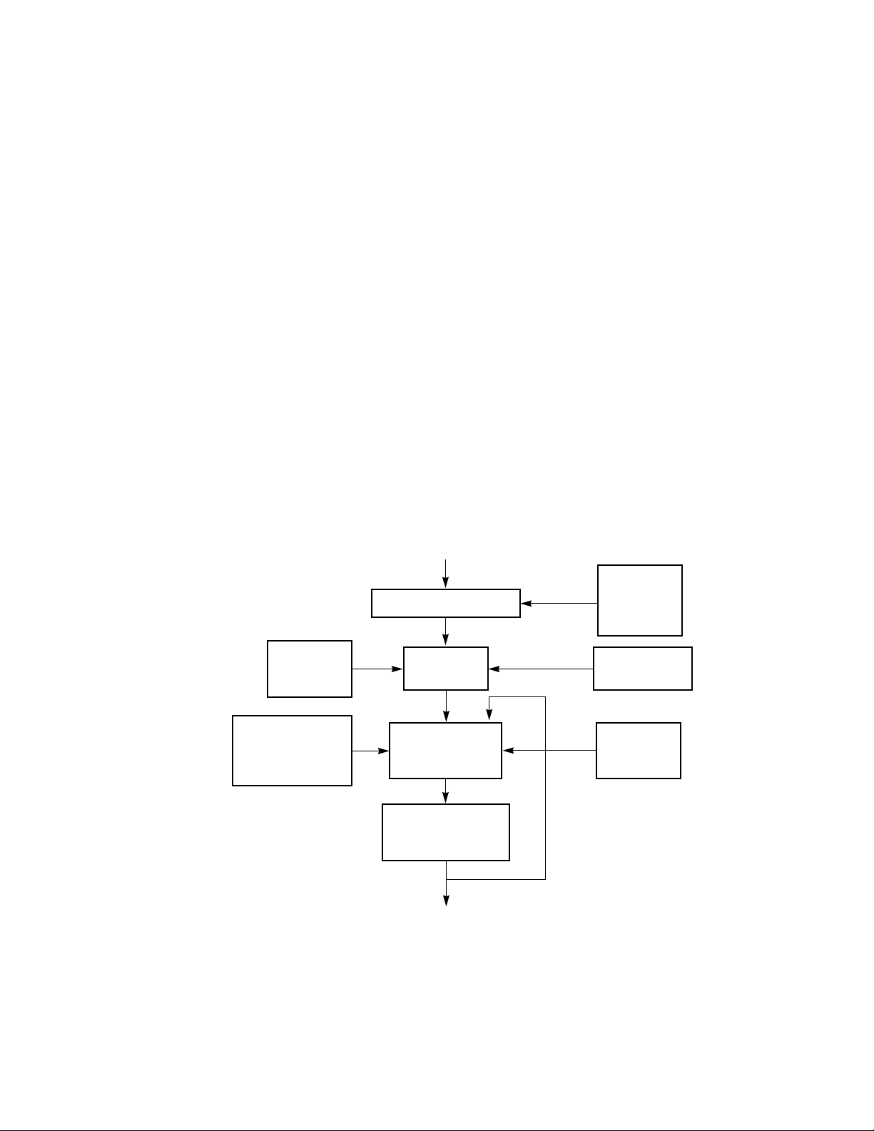
2.3.3 Graphics Controller
The graphics controller operates in either text or g raphics modes and has the follo wing major functions:
● Provides the host CPU with a read/write access path to display memory.
● Controls all four memory planes in planar modes (used for 16-color graphics).
● Allows data to be manipulated prior to being written to display memory.
● Formats data for use in various backward-compatibility modes.
● Provides color comparators for use in color painting modes.
● Reads/writes 32- or 64-bit words through the 32- or 64-bit display memory interface.
● Combines display memory data and attributes for output to the Pixel bus.
The graphics controller directs data from the display memory to the attribute controller and CPU.
Figure 2-3 and Figure 2-4 illustrate typical write and read operations.
For a write operation, the data from the CPU bus are combined with the data from the Set/Reset
logic, depending on the write and display modes. In addition, the data can be combined with the
contents of the read latches, and some bits or planes may be masked (prevented from being
changed). See the bit descriptions in Chapter 4, “VGA Core Registers”, for more information.
ENABLE
D[3:0]
WRITE MODE
AND DATA
MODE
FROM CPU DATA BUS
DATA ROTATOR
DATA
SELECT
FUNCTION
SELECTOR
PROCESSOR
LATCH
TO PLANES 0, 1, 2, 3
DATA
ROTATE
REGISTER
SET/RESET
D[3:0]
BIT
MASK
Figure 2-3. Graphics Controller Write Operation
Copyright 1996 – Cirrus Logic Inc. 2-7 November 1996

OVERVIEW CL-GD5446 Technical Reference Manual
The graphics controller is implemented when the CPU is reading data from display memory.
Depending on the read mode, the data returned may be the actual contents of the display memory
or reflect the outcome of comparisons with the color value in one of the Graphics Controller registers. See the descriptions in Chapter 4 for more information.
FROM PLANES 0, 1, 2, 3
READ MAP
REGISTER AND
READ MODE
PROCESSOR
LATCH
COLOR COMPARE
BITS 0–3
COMPARATOR
SELECTOR
COLOR DON’T CARE
BITS 0–3
PLANE
SELECT
TO CPU DATA BUS
Figure 2-4. Graphics Controller Read Operation
November 1996 2-8 Copyright 1996 – Cirrus Logic Inc.

CL-GD5446 Technical Reference Manual OVERVIEW
2.3.4 Attribute Controller
The attribute controller controls the blinking and underline attributes in alphanumeric modes. It
also provides horizontal pixel-panning capability in both alphanumeric and graphics modes. The
attribute controller registers are described in Chapter 4. Figure 2-5 is a functional block diagram
of the attribute controller.
OVERSCAN
REGISTER
PALETTE
DAC
P[7:0]
D[5:0]
ADDRESS REGISTER
AND DECODING
TIMING LOGIC
OUTPUT
LATCHES
AND
LOGIC
ATR[7:0]
CC[7:0]
ATTRIBUTE
LATCHES
AND
LOGIC
MODE CONTROL REGISTER
CONDITION CODE
SHIFT REGISTER
AND LOGIC
CURSOR BLINK
COUNTER
HORIZONTAL PIXEL
PANNING REGISTER
HORIZONTAL PIXEL
PANNING
SHIFT REGISTER
AND LOGIC
COLOR
PALETTE
REGISTERS
COLOR PLANE
ENABLE REGISTER
PALETTE
ADDRESS
AND DECODING
Figure 2-5. Attribute Controller
Copyright 1996 – Cirrus Logic Inc. 2-9 November 1996

OVERVIEW CL-GD5446 Technical Reference Manual
2.3.5 Programmable Dual-Frequency Synthesizer
The CL-GD5446 includes an integrated dual-frequency synthesizer that can be programmed to
generate the VCLK for all supported screen formats, and the MCLK used by the sequencer. The
VCLK synthesizer can support a pixel clock of up to 135 MHz. The MCLK synthesizer can be programmed for up to 80 MHz (for EDO DRAMS). The dual-frequency synthesizer includes an onchip oscillator that requires an inexpensive , two-pin 14.31818-MHz crystal. Alternatively, the dualfrequency synthesizer can use a reference frequency of 14.31818 MHz from an external source.
Figure 2-6 is a functional block diagram of the programmable dual-frequency synthesizer.
VCLK
SELECTION
CRYSTAL
MCLK
SELECTION
OSC
PROGRAMMABLE
VCLK
OSCILLATOR
PROGRAMMABLE MCLK
OSCILLATOR
VCLK
MCLK
Figure 2-6. Programmable Dual-Frequency Synthesizer Functional Diagram
November 1996 2-10 Copyright 1996 – Cirrus Logic Inc.

CL-GD5446 Technical Reference Manual OVERVIEW
2.3.6 Palette DAC
The CL-GD5446 includes an integrated palette DAC that can interface to an analog monitor connector through the appropriate RFI filters. The palette DAC can be programmed for 256 simultaneous colors from a palette of 256K, or it can be programmed for Direct-color mode . In Direct-color
mode, two, three, or four contiguous bytes from the display memory are combined for each pixel.
This allows 32K, 64K, or 16.8 million simultaneous colors on the screen.
The CL-GD5446 supports color space conversion and can display YUV 4:2:2 or AccuPak video
data as well as 8-bpp LUT and 16-bpp RGB in the hardware video window.
Figure 2-7 is a functional block diagram of the palette DAC.
P[31:0]
P[7:0]
VCLK
AccuPak DECODE,
VIDEO PIPELINE
ZOOMING, CSC
LOOKUP
TABLE
256 ×
18
MUX
DAC
R
G
B
Figure 2-7. 256-Color/Direct-Color Palette DAC
Copyright 1996 – Cirrus Logic Inc. 2-11 November 1996

OVERVIEW CL-GD5446 Technical Reference Manual
2.4 PCI Bus Interface
The CL-GD5446 includes a glueless 32-bit PCI bus interface . This interface features full PCI compliance, including optimized PCI burst write, which supports PCI writes to the frame buffer at
greater than 55 Mbytes per second.
The frame buffer is addressable through a 16-Mbyte window consisting of three 4-Mbyte byteswapping apertures, and a special video aperture. The VGA control registers are relocateable
anywhere in the 64-Kbyte space (allowing multiple devices in a single system).
The frame buffer in Revision B of the CL-GD5446 is addressable through two 16-Mbyte windows.
One window is for direct accesses to the frame b uffer; the second window is f or system-to-screen
BitBLTs. The V GA registers in Re vision B of the CL-GD5446 are accessible an ywhere in the memory address space. Revision B of the CL-GD5446 supports Subsystem Vendor ID in PCI2C.
2.5 BitBLT Engine
The CL-GD5446 includes a BitBL T engine f or block tr ansfers within displa y memory at full memory
bandwidth. System-to-display transfers can also be effected with the BitBLT engine.
The CL-GD5446 BitBLT engine suppor ts transparency with color expansion for all graphics formats and transparency without color expansion for 8- and 16-bpp graphics formats.
The BitBL T control registers are doub le-buff ered and memory-mapped. Doub le-buff ered registers,
in conjunction with the autostart feature, allow concurrent operation of the host and the BitBLT
engine. The host can prepare and load the par ameters f or operation n + 1 while the BitBLT engine
is executing operation n. When the current operation completes, the BitBLT engine automatically
loads and begins with the parameters for the next operation.
All 16 two-operand ROPs (raster operations) are implemented in hardware. Color expansion
leverages host bandwidth by up to 32 times.
HOST INTERFACE
DOUBLE-BUFFERED
REGISTERS
COLOR EXPANSION
COLORS
WORKING
REGISTERS
64-BIT DATA FLOW
TRANSPARENCY
COLORS
FRAME
BUFFER
Figure 2-8. BitBLT Engine
November 1996 2-12 Copyright 1996 – Cirrus Logic Inc.

CL-GD5446 Technical Reference Manual OVERVIEW
2.6 Video Capture
The CL-GD5446 V-Port accepts video data from a realtime or recorded source and stores it
into the frame buffer. V-Por t can accept data in YUV 4:2:2, RGB16, or AccuPak formats.
Figure 2-9 shows a V-Port functional block diagram.
Video data can be converted from YUV 4:2:2 to AccuP ak as it is being stored, or it can be decimated as it is being stored. Decimation and AccuPak conversion cannot be used together.
Horizontal and vertical decimation are independently specified. In addition, temporal decimation can be used.
The video capture address can come from either of two register sets, allowing automatic double buffering. When this is used, the video buffers being used for capture and display can be
automatically swapped, ensuring that partial images are not displayed.
The CL-GD5446 has an independent video capture FIFO, allowing simultaneous video capture and occlusion or interpolated Y-zooming (subject to frame buffer bandwidth restrictions).
DECIMATION
CONTROL
V-Port
Figure 2-9. V-Port Functional Block Diagram
2.7 Video Window and Video Display
The CL-GD5446 has a video window timing generator that defines a rectangular area on the
display. This area can display video data or mixed graphics and video data. Video data can
(and typically does) have a for mat different from Graphics data. Typically, Video data also
comes from a separate area in the frame buffer.
YUV (4:2:2 in CCIR601 encoding) data is color space converted to RGB in the video pipeline.
AccuPak data is expanded to YUV 4:2:2 prior to color space conversion.
CAPTURE ADDRESS
GENERATOR LOGIC
VIDEO CAPTURE FIFO
YUV TO ACCUPAK
FRAME
BUFFER
Video data can be zoomed for display in the video window. Zoom factors in the range of 1
through 4 are generally used. X-zooming is always done with interpolation (the intermediate
pixels values are a w eighted av erage of ‘real’ pixels). Y-zooming can be done with interpolation
(2× or above) or line replication. Inter polation zooming produces superior results and should
be used whenever bandwidth requirements permit.
Copyright 1996 – Cirrus Logic Inc. 2-13 November 1996

OVERVIEW CL-GD5446 Technical Reference Manual
The CL-GD5446 has support for occlusion in the video window. This permits Graphics data and
Video data to be mixed on a pixel-b y-pix el basis. Color keying the Graphics data or chroma keying
the Video data can determine which pixels to replace corresponding pix els from the alternate data
stream.
2.7.1 DDC2B/I
The CL-GD5446 supports a two-pin I
peripherals such as TV tuners with an I
2
C Support
2
C interface used for DDC2B support. It can also control
2
C interface.
2.7.2 General-Purpose I/O Port
The CL-GD5446 provides address decoding and an 8- or 16-bit data bus f or an additional peripheral device on the same adapter board as the GUI-X. The CL-GD5446 provides address and data
buffering to comply with the PCI ‘one-load’ specification. The base address of the port is specified
in a PCI configuration register. The port can be in I/O space or memory space.
2.8 Hardware/Software Compatibility
The CL-GD5446 is compatible with the IBM VGA standard.
2.9 Computer Display Subsystem Architecture
Figure 2-10 shows the main components required to implement a functional VGA subsystem
using the CL-GD5446. The interfaces that must be implemented are the host CPU, the BIOS (for
adapter board implementation only), the display memory, and the CRT. If video is required, the VPort interface must be implemented.
V-Port
INTERFACE
GPIO
I2C
MONITOR
SYSTEM BUS
ROM
DISPLAY
MEMORY
CL-GD5446
Figure 2-10. Computer Display Subsystem Architecture
November 1996 2-14 Copyright 1996 – Cirrus Logic Inc.

3
Data Book

DATA BOOK CL-GD5446 Technical Reference Manual
3. DATA BOOK
November 1996 3-ii Copyright 1996 – Cirrus Logic Inc.

FEATURES
■ High-throughput PCI bus interface optimized for video
playback
— Large write buff er allo ws sustained z ero-w ait-state bursts
— Independent memory apertures for BitBLT and CPU/video
allow concurrent operations for optimized video pla yback
— Byte-swapping for PowerPC support
— PCI v2.1-compliant
■ Advanced 64-bit BitBLT engine for Windows 95
— Transparent source data BitBLT for DirectDraw
— Color expansion for all graphics modes
— Large data buffers for fast screen-to-screen BitBLTs
— Double-b uffered, memory-mapped registers with AutoStart
— Optimized color 8 × 8 PatCopy
— Accelerated Packed-24 modes
■ 64-bit DRAM interface optimized for EDO DRAM
— 80-MHz MCLK offers up to 320 Mbytes/sec. peak bandwidth
— Supports new 128K × 16, 128K × 32 DRAM
■ V-Port, GPIO, I2C bus interfaces for video decoders
— Video capture, closed-caption capture applications
— GPIO permits video decoders with single load on PCI bus
— Automatic double buffering prev ents video ‘tearing’
— Glueless interface to the CL-PX4072
— Interface to MPEG and other video decoders
■ Hardware window for video display
— Multiformat frame buffer
— Supports YUV -16 true color video with 8-bit graphics
— YUV 4:2:2, AccuP ak, RGB-8, RGB-16 video formats
— Unique YUV planar assist mode
— Independent interpolated X and Y zooming
— Occlusion support with color- or chroma-key
■ PC97-compliant (Revision B)
(cont.)
CL-GD5446
Preliminary Data Book
64-bit
VisualMedia Accelerator
OVERVIEW
The CL-GD5446 delivers high-performance graphics and TVquality , full-motion, full-screen video pla yback in an integrated,
single-chip device. The CL-GD5446 VisualMedia accelerator, integrated into a cost-effective personal computer, plays
CD-ROM video clips and disk-based video files (including
MPEG titles), in full screen at up to 30 frames per second with
fully synchronized sound. At the same time, the CL-GD5446
delivers exceptional system throughput with minimal impact to
system operation. Transparent BitBLT and page-flipping features provide outstanding DirectDraw and games performance.
The CL-GD5446 provides a glueless connection to most of the
popular video decoder devices from Cirrus Logic as well as
other vendors. This provides broad flexibility to support live TV in-a-window, closed captioning, hardware MPEG, and video
conferencing, extending baseline system functions with
enhanced features to meet the requirements of a wide range
of applications.
The CL-GD5446 can support YUV 4:2:2 video playback in an
arbitrarily sized window on 1024 × 768, 256-color graphics
with a frame buffer of only 1 Mbyte. This capability can help
place PCs using the CL-GD5446 at a very fav orable price-performance point.
The CL-GD5446 supports pixel resolutions of up to
1280 × 1024, and 16.8 million colors at resolutions of up to
1024 × 768.
(cont.)
System
Block Diagram
MPEG
DECODER
(Optional)
TV
DECODER
(Optional)
DRAM
GPIO
CL-GD5446
V-Port
2
C
I
HARD DRIVE CD-ROM
208-Pin PQFP
PCI BUS
CRT DISPLAY
November 1996Version 2.0

O VERVIEW
CL-GD5446
64-bit VisualMedia Accelerator
FEATURES
■ Product differentiation for video-pla yback applications
— Home PC television tuner: ‘TV-in-a-window’
— Video clip capture
— Home video editing
— Video mail/video message
— Personal video conferencing
— MPEG-1, MPEG-2 applications
— Closed-caption applications
■ Cirrus Logic provides enabling software drivers
— Windows 95, Windows 3.x, NT, OS/2, and AutoCAD
— DirectDraw and DCI
— VPM (video port manager)
(cont.)
OVERVIEW
The CL-GD5446 features an integrated dual-frequency synthesizer with on-chip oscillator and filters, as well as a triple
8-bit palette DAC with on-chip current reference. Green-PC
power-management features help make systems based on
the CL-GD5446 compliant with the Energy Star Program.
The CL-GD5446 is software- and pin-compatible with the
industry-standard Alpine family of V GA controllers from Cirrus
Logic. It comes with the same Cirrus Logic quality software,
applications support, and documentation.
Revision B of the CL-GD5446 is PC97-compliant.
Cirrus Logic also provides TV decoder application softw are —
TVT ap — for the CL-GD5446/’PX407X designs.
(cont.)
ADVANTAGES
Unique Features Benefits
Outstanding VisualMedia Acceleration
■ High-throughput PCI bus interface ❒ Minimizes host bus bottleneck for VisualMedia playback.
■ Advanced 64-bit BitBLT engine with transparent BitBLT
and page-flip support
■ Optimized EDO DRAM interface ❒ 64-bit and 80-MHz MCLK offer best performance for
■ 128K × 16/32-bit DRAM options ❒ Allows 3- and 1-Mbyte (64-bit) options.
❒ Supports Fast Windows
mainstream DRAMs.
Superior TV -Like-Quality Video Perf ormance
■ Hardware video window ❒ Allows independent graphics and video streams to be
displayed on-screen.
■ X and Y linear interpolated scaling ❒ Minimizes aliasing and allows best video display regardless
of screen size.
■ YUV planar assist, AccuPak
■ Multiformat frame buffer ❒ Allows true-color video with 256-color graphics.
■ Color key, chroma key ❒ Allows graphics over video in video playback and video
encoding ❒ Technology to obtain best performance while minimizing
video-quality degradation.
capture modes.
Foundation for Differentiation
■ Video capture V-Port ❒ Allows video decoder interface and eliminates separate
frame buffer for lower system cost.
■ General-purpose I/O bus ❒ Allows single load, glueless, generic I/O interfacing to
industry-standard video decoders.
■ VPM
■ I
❒ Video port API for Windows
peripheral application software development.
2
C interface ❒ Allows low-cost control interface f or applications such as TV
decoders.
Compatibility
■ Compatible with VGA and VESA standards ❒ Compatible with installed base of systems and software.
■ Drivers supplied at various resolutions for Windows
Windows NT, AutoCAD
applications
, OS/2, and other popular
3.1,
❒ Provides a ‘ready-to-go’ solution minimizing the need for
additional driver development.
95, DirectDraw, and games.
v3.x and Windows 95 easing
OVERVIEW
PRELIMINARY DATA BOOK v2.0
November 19963-2

CL-GD5446
64-bit VisualMedia Accelerator
SOFTWARE SUPPORT
Cirrus Logic provides an extensive — and expanding — range of software drivers to enhance the resolution and performance of many popular software packages . Note that the CL-GD5446 VGA g r aphics portion of a system
software drivers to run applications in standard-resolution modes.
Cirrus Logic software drivers for the CL-GD5446 include:
does not
require
Software Drivers Resolution Supported
Microsoft / Intel DCI (display
control interface), DirectDraw,
VPM Provider
Microsoft
Microsoft
Microsoft
v4.0
OS/2
AutoCAD
Autoshade
3D Studio v1.0, v2.0, v3.0, v4.0
Windows v3.x
Windows 95
Windows NT v3.5, v3.51,
v2.11, v3.0
v12.0, v13.0
v2.0 with Renderman
a
640 × 480, 800 × 600, 1024 × 768, 1152 × 864, 1280 × 1024 256
640 × 480, 800 × 600, 1024 × 768, 1152 × 864, 1280 × 1024 65,536
640 × 480, 800 × 600, 1024 × 768 16.8 million
640 × 480, 800 × 600, 1024 × 768, 1152 × 864, 1280 × 1024 256
640 × 480, 800 × 600, 1024 × 768, 1152 × 864, 1280 × 1024 65,536
640 × 480, 800 × 600, 1024 × 768 16.8 million
640 × 480, 800 × 600, 1024 × 768, 1152 × 864, 1280 × 1024 16 and 256
640 × 480, 800 × 600, 1024 × 768, 1152 × 864, 1280 × 1024 65,536
640 × 480, 800 × 600, 1024 × 768 16.8 million
640 × 480, 800 × 600, 1024 × 768,1280 × 1024 256
640 × 480, 800 × 600, 1024 × 768, 1280 × 1024 65,536
640 × 480, 800 × 600, 1024 × 768 16.8 million
640 × 480, 800 × 600, 1024 × 768, 1280 × 1024 16
640 × 480, 800 × 600, 1024 × 768, 1280 × 1024 256
640 × 480, 800 × 600, 1024 × 768 32,768
640 × 480, 800 × 600, 1024 × 768 65,536
No. of Colors
640 × 480, 800 × 600, 1024 × 768 16.8 million
a
All monitor types do not support all resolutions; 640 × 480 drivers will run on PS/2-type monitors. Extended resolutions are dependent upon
monitor type and VGA system implementation.
BIOS SUPPORT
■ Fully IBM VGA-compatible BIOS
■ Relocatable, 32 Kbytes with PCI b us support
■ VBE (VESA BIOS Extensions) support in ROM
■ Support for DPMS (display power management
signaling) in ROM
■ VESA
■ DDC1/2B support
November 1996 3-3
monitor timing-compliant
PRELIMINARY DATA BOOK v2.0 OVERVIEW
UTILITIES
■ Graphics and video diagnostics test
■ Windows
■ Video mode configuration utility — CLMODE
■ Set resolution in Windows
■ Configurable system integration for OEMs — OEMSI
NT and DOS utilities
utility — WINMODE

CL-GD5446
64-bit VisualMedia Accelerator
CONTENTS
CONVENTIONS......................................................................................3-5
1.PIN INFORMATION................................................................................3-7
1.1Pin Summary..........................................................................................................3-8
2.FUNCTIONAL DESCRIPTION..............................................................3-20
2.1General.................................................................................................................3-20
2.2Functional Blocks..................................................................................................3-21
2.2.1 CPU Interface.........................................................................................3-21
2.2.2 CPU Write Buffer....................................................................................3-21
2.2.3 Graphics Controller................................................................................3-21
2.2.4 BitBLT Engine.........................................................................................3-21
2.2.5 Memory Arbitrator...................................................................................3-21
2.2.6 Memory Sequencer................................................................................3-21
2.2.7 CRT Controller........................................................................................3-21
2.2.8 Display FIFOs.........................................................................................3-22
2.2.9 Attribute Controller.................................................................................3-22
2.2.10 V-Port..................................................................................................3-22
2.2.11 Hardware Video Window........................................................................3-22
2.2.12 Palette DAC............................................................................................3-22
2.2.13 Dual-Frequency Synthesizer..................................................................3-22
2.2.14 VESA/VGA Pass-Through Connector..................................................3-23
2.2.15 General-Purpose I/O Port.......................................................................3-23
2.2.16 I2C Interface...........................................................................................3-23
2.3Performance..........................................................................................................3-23
2.4Compatibility.........................................................................................................3-23
2.5Board Testability....................................................................................................3-23
3.CONFIGURATION TABLES..................................................................3-24
3.1Graphics Modes....................................................................................................3-24
3.2Configuration Register, CF....................................................................................3-28
4.VGA REGISTER PORT MAP................................................................3-29
5.REGISTER MAP...................................................................................3-30
6.PACKAGE SPECIFICATIONS..............................................................3-36
7.ORDERING INFORMATION EXAMPLE...............................................3-37
Revision History
The following are the differences between the December 1995 and November 1996 versions of this data book:
● Information pertaining to the Revision B device has been added
PRELIMINARY DATA BOOK v2.0
November 19963-4

CL-GD5446
64-bit VisualMedia Accelerator
CONVENTIONS
Abbreviations
Symbol Units of measure
°C degree Celsius
Hz hertz (cycles per second)
Kbyte kilobyte (1,024 bytes)
kHz kilohertz
kΩ kilohm
Mbyte megabyte (1,048,576 bytes)
MHz megahertz (1,000 kilohertz)
µF microfarad
µs microsecond (1,000 nanoseconds)
mA milliampere
ms millisecond (1,000 microseconds)
ns nanosecond
pV picovolt
The use of ‘tbd’ indicates values that are ‘to be determined’, ‘n/a’ designates ‘not available’, and ‘n/c’ indicates a pin that is a ‘no connect’.
Numeric Naming
Hexadecimal numbers are represented with all letters in upper case and a lower-case ‘h’ is appended to
them (for example, ‘14h’, ‘3A7h’, and ‘C000h’ are hexadecimal numbers). Binar y numbers are represented with a lower-case ‘b’ appended. Numbers not indicated by a ‘b’ or an ‘h’ are decimal.
Acronyms
Acronym Definition
AC alternating current
ALU arithmetic logic unit
ATE automatic test equipment
BIOS basic input/output system
BitBLT, BLT bit boundary block transfer
bpp bits per pixel
CAD computer-aided design
CAS column address strobe
CGA color graphics adapter
Acronym Definition
CLUT color lookup table
CMOS complementary metal-oxide
semiconductor
CPU central processing unit
CRT cathode ray tube
CRTC CRT controller
DAC digital-to-analog converter
DC direct current
DDA digital differential algorithm
November 1996 3-5
PRELIMINARY DATA BOOK v2.0 CONVENTIONS

CL-GD5446
64-bit VisualMedia Accelerator
Acronym Definition
DDC display data channel
DMI desktop management signaling
DPMS display power management
DRAM dynamic random access memory
dword doubleword
EEPROM electrically erasable/programmable
EGA enhanced graphics adapter
EPROM electrically programmable read-only
EV AFC extended VESA
FIFO first in/first out
GPIO general-purpose IO
GSC graphics system controller
GUI graphical user interface
HDR Hidden DAC register
HRQ host read queue
HSYNC/VSYNC horizontal/vertical synchronization
HWQ host write queue
IC integrated circuit
I/O input/output
LBI local bus interface
LSB least-significant bit
LUT lookup table
MA memory arbiter
MC memory controller
signaling
read-only memory
memory
connector
advanced feature
Acronym Definition
PCI peripheral component
PFS programmable frequency
PLL phase-locked loop
PQFP plastic quad-flat pack
qword two dwords
RAC Rambus
RAM random-access memory
RAS row address strobe
RDRAM Rambus dynamic random-access
RGB red, green, and blue
RIF Rambus
ROPs raster operations
RSU result storage unit
R/W read/write
SC serial clock
SG signature generator
SGRAM synchronous graphics RAM
SRAM static random-access memory
TSR terminate and stay resident
TTL transistor-transistor logic
VBE VESA BIOS extensions
VBI vertical blanking interval
VDD virtual device driver
VESA
interconnect
synthesizer
access channel
memory
interface
Video Electronics Standards
Association
MCC monochrome-to-color converter
MD memory data
MMI/O memory-mapped I/O
MSB most-significant bit
OFU operand fetch unit
OSU operand storage unit
CONVENTIONS
VGA video graphics array
VL VESA
VPM video port manager
VRAM video random-access memory
WE transparency write enable
PRELIMINARY DATA BOOK v2.0
local
November 19963-6

104
103
102
101
100
99
98
97
96
95
94
93
92
91
90
89
88
87
86
85
84
83
82
81
80
79
78
77
76
75
74
73
72
71
70
69
68
67
66
65
64
63
62
61
60
59
58
57
56
55
54
53
123456789101112131415161718192021222324252627282930313233343536373839404142434445464748495051
52
156
155
154
153
152
151
150
149
148
147
146
145
144
143
142
141
140
139
138
137
136
135
134
133
132
131
130
129
128
127
126
125
124
123
122
121
120
119
118
117
116
115
114
113
112
111
110
109
108
107
106
105
157
158
159
160
161
162
163
164
165
166
167
168
169
170
171
172
173
174
175
176
177
178
179
180
181
182
183
184
185
186
187
188
189
190
191
192
193
194
195
196
197
198
199
200
201
202
203
204
205
206
207
208
VDD1
MD32
CAS4#
CAS0#
MD7/BIOSD7
MD6/BIOSD6
MD5/BIOSD5
MD4/BIOSD4
MD3/BIOSD3
MD2/BIOSD2
MD1/BIOSD1
MD0/BIOSD0
MCLKVDD
XTAL
MCLKVSS
MCLK
OSC
VSS1
INTR#
C/BE#0
C/BE#1
C/BE#2
C/BE#3
BIOSA0
BIOSA1
BIOSA2
BIOSA3
BIOSA4
BIOSA5
BIOSA6
BIOSA7
BIOSA8
EROM#
BIOSA9
BIOSA10/ P15
BIOSA11/ P14
BIOSA12/ P13
RESERVED/ P12
RESERVED/ P11
BIOSA13/ P10
BIOSA14
BIOSA15
CLK
RESERVED/ P9
RESERVED/ P8
FRAME#
IRDY#
STOP#
TRDY#
PAR
RST#
VSS2
VSS6
IREF
RED
GREEN
BLUE
DACVDD
HSYNC
DACVSS
VSYNC
VCLKVDD
RSET
VCLKVSS
AD0
AD1
AD2
AD3
AD4
AD5
VSS5
AD6
AD7
VDD3
AD8
AD9
AD10
AD11
AD12
VSS4
AD13
AD14
AD15
AD16
AD17
AD18
AD19
AD20
AD21
VSS3
RESERVED
DEVSEL#
VDD2
AD22
AD23
AD24
AD25
AD26
AD27
AD28
AD29
AD30
AD31
IDSEL
CL-GD5446
208-Pin PQFP/HQFP
PCI Bus
CAS1#
MD8
MD9
MD10
MD11
MD12
VSS9
MD13
MD14
MD15
VDD5
CAS2#
MD16
MD17
MD18
MD19
MD20
MD21
MD22
MD23
VSS8
CAS3#
MD24
MD25
MD26
MD27
MD28
MD29
MD30
MD31
BLANK#
DCLK
VSS7
EDCLK#
ESYNC#
VDD4
EVIDEO#
DACVSS P7P6P5P4
DACVDDP3P2P1P0
OVRW#
RESERVED
DDCCLK
DDCDAT
TWR#
MD63
MD62
MD61
MD60
MD59
MD58
MD57
MD56
VSS10
CAS7#
WE#
RAS1#
RAS0#
MD55
MD54
MD53
MD52
MD51
MD50
MD49
MD48
VDD6
CAS6#
MA0
VSS11
MA1
MA2
MA3
MA4
MA5
MA6
MA7
MA8
MA9
MD47
MD46
MD45
MD44
VSS12
MD43
MD42
MD41
MD40
CAS5#
MD39
MD38
MD37
MD36
MD35
MD34
MD33
VSS13
CL-GD5446
64-bit VisualMedia Accelerator
1. PIN INFORMATION
The CL-GD5446 VGA GUI controller is available in a 208-pin PQFP (plastic quad flat pack) or HQFP
(high-performance quad flat pack) for the PCI bus only.
November 1996 3-7
PRELIMINARY DATA BOOK v2.0 PIN INFORMATION

PIN INFORMATION
CL-GD5446
64-bit VisualMedia Accelerator
1.1 Pin Summary
The following abbreviations are used for pin types in the following tables: (I) indicates input; (O) indicates
output; (O-Z) indicates tristate output; (OC) indicates open-collector output; (BIO) indicates bidirectional
I/O; (I/O) indicates input or output depending on how the device is configured and programmed.
Table 1-1. Host Interface
Pin
Number
53 I IDSEL
51 I RST#
46 I FRAME#
47 I IRDY#
43 I CLK
49 BIO −3 8 240 TRDY#
48 BIO −3 8 240 STOP#
50 O −3 8 240 PAR
65 O −3 4 200 DEVSEL#
19 OC (OC) 24 200 INTR#
54 BIO −3 12 240 AD31
55 BIO −3 12 240 AD30
56 BIO −3 12 240 AD29
Pin
Type
Pull-up
IOH
a
(mA)
IOL
(mA)
Load
(pF)
PCI
b
GPIO
Redefinition
Pixel Bus
c
Redefinition
57 BIO −3 12 240 AD28
58 BIO −3 12 240 AD27
59 BIO −3 12 240 AD26
60 BIO −3 12 240 AD25
61 BIO −3 12 240 AD24
62 BIO −3 12 240 AD23
63 BIO −3 12 240 AD22
68 BIO −3 12 240 AD21
69 BIO −3 12 240 AD20
70 BIO −3 12 240 AD19
71 BIO −3 12 240 AD18
72 BIO −3 12 240 AD17
73 BIO −3 12 240 AD16
PIN INFORMATION
PRELIMINARY DATA BOOK v2.0
November 19963-8

CL-GD5446
64-bit VisualMedia Accelerator
Table 1-1. Host Interface
Pin
Number
74 BIO −3 12 240 AD15
75 BIO −3 12 240 AD14
76 BIO −3 12 240 AD13
78 BIO −3 12 240 AD12
79 BIO −3 12 240 AD11
80 BIO −3 12 240 AD10
81 BIO −3 12 240 AD9
82 BIO −3 12 240 AD8
84 BIO −3 12 240 AD7
85 BIO −3 12 240 AD6
87 BIO −3 12 240 AD5
88 BIO −3 12 240 AD4
89 BIO −3 12 240 AD3
Pin
Type
Pull-up
(cont.)
a
IOH
(mA)
IOL
(mA)
Load
(pF)
PCI
b
GPIO
Redefinition
Pixel Bus
c
Redefinition
90 BIO −3 12 240 AD2
91 BIO −3 12 240 AD1
92 BIO −3 12 240 AD0
23 I C/BE#3
22 I C/BE#2
21 I C/BE#1
20 I C/BE#0
42 I/O −3 8 50 BIOSA15 GPA1
41 I/O −3 8 50 BIOSA14 GPA0
40 I/O −3 8 50 BIOSA13 GPD10 P10
37 I/O −3 8 50 BIOSA12 GPD13 P13
36 I/O −3 8 50 BIOSA11 GPD14 P14
35 I/O −3 8 50 BIOSA10 GPD15 P15
34 I/O −3 8 50 BIOSA9 GPIOWR#
32 I/O −3 8 50 BIOSA8 GPIORD#
31 I/O −3 8 50 BIOSA7 GPD7
30 I/O −3 8 50 BIOSA6 GPD6
November 1996 3-9
PRELIMINARY DATA BOOK v2.0 PIN INFORMATION

CL-GD5446
64-bit VisualMedia Accelerator
Table 1-1. Host Interface
Pin
Number
29 I/O −3 8 50 BIOSA5 GPD5
28 I/O −3 8 50 BIOSA4 GPD4
27 I/O −3 8 50 BIOSA3 GPD3
26 I/O −3 8 50 BIOSA2 GPD2
25 I/O −3 8 50 BIOSA1 GPD1
24 I/O −3 8 50 BIOSA0 GPD0
66 I/O −3 8 50 Reserved GPRDY/DT
45 I/O −3 8 50 Reserved GPD8 P8
44 I/O −3 8 50 Reserved GPD9 P9
39 I/O −3 8 50 Reserved GPD11 P11
38 I/O −3 8 50 Reserved GPD12 P12
a
Indicates nominal 250-kΩ pull-up resistor.
b
See Appendix B11 for additional information on the general-purpose I/O port.
c
See the definition of register GR18[6].
Pin
Type
Pull-up
(cont.)
a
IOH
(mA)
IOL
(mA)
Load
(pF)
PCI
b
GPIO
Redefinition
Pixel Bus
c
Redefinition
Table 1-2. Video Interface
Pin
Number
96 O-Z −12 24 50 VSYNC
98 O-Z −12 24 50 HSYNC
126 I/O −12 12 50 BLANK# HREF Input
35 I/O −3 8 50 P15
36 I/O −3 8 50 P14
37 I/O −3 8 50 P13
38 I/O −3 8 50 P12
39 I/O −3 8 50 P11
40 I/O −3 8 50 P10
44 I/O −3 8 50 P9
45 I/O −3 8 50 P8
118 I/O −12 12 50 P7 PIXD7
117 I/O −12 12 50 P6 PIXD6
Pin
Type
Pull-up
a
IOH (mA) IOL (mA) Load (pF) Name
Redefinition
b
b
b
b
b
b
b
b
V-Port
PIXD15
PIXD14
PIXD13
PIXD12
PIXD11
PIXD10
PIXD9
PIXD8
PIN INFORMATION
PRELIMINARY DATA BOOK v2.0
November 19963-10

CL-GD5446
64-bit VisualMedia Accelerator
Table 1-2. Video Interface
Pin
Number
116 I/O −12 12 50 P5 PIXD5
115 I/O −12 12 50 P4 PIXD4
113 I/O −12 12 50 P3 PIXD3
112 I/O −12 12 50 P2 PIXD2
111 I/O −12 12 50 P1 PIXD1
110 I/O −12 12 50 P0 PIXD0
125 I/O −12 12 50 DCLK PIXCLK Input
122 I/O
120 I/O
123 I
102 Analog Out RED
101 Analog Out GREEN
100 Analog Out BLUE
Pin
Type
(cont.)
Pull-up
●
●
●
a
IOH (mA) IOL (mA) Load (pF) Name
−12 12 ESYNC
−12 12 EVIDEO# VACT Input
Redefinition
#
EDCLK# VREF Input
(Prog. Output 1)
V-Port
103 Analog In IREF
94 Analog In RSET
a
● indicates the presence of an internal 250-kΩ ±50% pull-up resistor.
b
P[15:8] are redefined PCI pins. See the definition of register GR18[6].
Table 1-3. Display Memory Interface
Pin Number Pin Type Pull-up
168 O −12 12 50 RAS1#
169 O −12 12 50 RAS0#
166 O −12 12 50 CAS7#
179 O −12 12 50 CAS6#
200 O −12 12 50 CAS5#
3O −12 12 50 CAS4#
135 O −12 12 50 CAS3#
145 O −12 12 50 CAS2#
156 O −12 12 50 CAS1#
a
IOH (mA) IOL (mA) Load (pF) Name
4O −12 12 50 CAS0#
November 1996 3-11
PRELIMINARY DATA BOOK v2.0 PIN INFORMATION

CL-GD5446
64-bit VisualMedia Accelerator
Table 1-3. Display Memory Interface
Pin Number Pin Type Pull-up
(cont.)
a
IOH (mA) IOL (mA) Load (pF) Name
167 O −12 12 150 WE#
190 O −12 12 150 MA9
189 O −12 12 150 MA8
188 O −12 12 150 MA7
187 O −12 12 150 MA6
186 O −12 12 150 MA5
185 O −12 12 150 MA4
184 O −12 12 150 MA3
183 O −12 12 150 MA2
182 O −12 12 150 MA1
180 O −12 12 150 MA0
157 I/O
158 I/O
●
●
−8 8 50 MD63
−8 8 50 MD62
b
c
159 I/O
160 I/O
161 I/O
162 I/O
163 I/O
164 I/O
170 I/O
171 I/O
172 I/O
173 I/O
174 I/O
175 I/O
176 I/O
177 I/O
191 I/O
192 I/O
●
●
●
●
●
●
●
●
●
●
●
●
●
●
●
●
−8 8 50 MD61
−8 8 50 MD60
−8 8 50 MD59
−8 8 50 MD58
−8 8 50 MD57
−8 8 50 MD56
−8 8 50 MD55
−8 8 50 MD54
−8 8 50 MD53
−8 8 50 MD52
−8 8 50 MD51
−8 8 50 MD50
−8 8 50 MD49
−8 8 50 MD48
−8 8 50 MD47
−8 8 50 MD46
193 I/O
194 I/O
PIN INFORMATION
●
●
−8 8 50 MD45
−8 8 50 MD44
PRELIMINARY DATA BOOK v2.0
November 19963-12

CL-GD5446
64-bit VisualMedia Accelerator
Table 1-3. Display Memory Interface
Pin Number Pin Type Pull-up
196 I/O
197 I/O
198 I/O
199 I/O
201 I/O
202 I/O
203 I/O
204 I/O
205 I/O
206 I/O
207 I/O
2 I/O
127 I/O
●
●
●
●
●
●
●
●
●
●
●
●
●
(cont.)
a
IOH (mA) IOL (mA) Load (pF) Name
−8 8 50 MD43
−8 8 50 MD42
−8 8 50 MD41
−8 8 50 MD40
−8 8 50 MD39
−8 8 50 MD38
−8 8 50 MD37
−8 8 50 MD36
−8 8 50 MD35
−8 8 50 MD34
−8 8 50 MD33
−8 8 50 MD32
−8 8 50 MD31
128 I/O
129 I/O
130 I/O
131 I/O
132 I/O
133 I/O
134 I/O
137 I/O
138 I/O
139 I/O
140 I/O
141 I/O
142 I/O
143 I/O
144 I/O
147 I/O
●
●
●
●
●
●
●
●
●
●
●
●
●
●
●
●
−8 8 50 MD30
−8 8 50 MD29
−8 8 50 MD28
−8 8 50 MD27
−8 8 50 MD26
−8 8 50 MD25
−8 8 50 MD24
−8 8 50 MD23
−8 8 50 MD22
−8 8 50 MD21
−8 8 50 MD20
−8 8 50 MD19
−8 8 50 MD18
−8 8 50 MD17
−8 8 50 MD16
−8 8 50 MD15
148 I/O
149 I/O
November 1996 3-13
PRELIMINARY DATA BOOK v2.0 PIN INFORMATION
●
●
−8 8 50 MD14
−8 8 50 MD13

CL-GD5446
64-bit VisualMedia Accelerator
Table 1-3. Display Memory Interface
Pin Number Pin Type Pull-up
151 I/O
152 I/O
153 I/O
154 I/O
155 I/O
5 I/O
6 I/O
7 I/O
8 I/O
9 I/O
10 I/O
11 I/O
12 I/O
●
●
●
●
●
●
●
●
●
●
●
●
●
(cont.)
a
IOH (mA) IOL (mA) Load (pF) Name
−8 8 50 MD12
−8 8 50 MD11
−8 8 50 MD10
−8 8 50 MD9
−8 8 50 MD8
−8 8 50 MD7/BIOSD7
−8 8 50 MD6/BIOSD6
−8 8 50 MD5/BIOSD5
−8 8 50 MD4/BIOSD4
−8 8 50 MD3/BIOSD3
−8 8 50 MD2/BIOSD2
−8 8 50 MD1/BIOSD1
−8 8 50 MD0/BIOSD0
d
d
d
d
d
d
d
d
a
● indicates the presence of an internal 250-kΩ ±50% pull-up resistor.
b
MA8 is connected to Memory Address 0 for asymmetric DRAMs.
c
MA0 is connected to Memory Address 8 for asymmetric DRAMs.
d
MD[7:0] are also used as the BIOS Data Input pins.
Table 1-4. General-Purpose I/Oa Port
Pin Number Pin Type IOH (mA) IOL (mA) Load (pF) Pin Name Redefined As
35 I/O −3 8 50 BIOSA10 GPD15
36 I/O −3 8 50 BIOSA11 GPD14
37 I/O −3 8 50 BIOSA12 GPD13
38 I/O −3 8 50 Reserved GPD12
39 I/O −3 8 50 Reserved GPD11
40 I/O −3 8 50 BIOSA13 GPD10
44 I/O −3 8 50 Reserved GPD9
45 I/O −3 8 50 Reserved GPD8
31 I/O −3 8 50 BIOSA7 GPD7
30 I/O −3 8 50 BIOSA6 GPD6
29 I/O −3 8 50 BIOSA5 GPD5
28 I/O −3 8 50 BIOSA4 GPD4
PIN INFORMATION
PRELIMINARY DATA BOOK v2.0
November 19963-14

CL-GD5446
64-bit VisualMedia Accelerator
Table 1-4. General-Purpose I/Oa Port
Pin Number Pin Type IOH (mA) IOL (mA) Load (pF) Pin Name Redefined As
27 I/O −3 8 50 BIOSA3 GPD3
26 I/O −3 8 50 BIOSA2 GPD2
25 I/O −3 8 50 BIOSA1 GPD1
24 I/O −3 8 50 BIOSA0 GPD0
14 I/O −3 8 50 XTAL GPA6
42 I/O −3 8 50 BIOSA15 GPA5/GPA1
41 I/O −3 8 50 BIOSA14 GPA4/GPA0
109 O −3 8 50 OVRW# GPA3
105 I/O −3 8 50 TWR# GPA2
108 O −3 8 50 Reserved GPCS#
32 I/O −3 8 50 BIOSA8 GPIORD#
34 I/O −3 8 50 BIOSA9 GPIOWR#
66 I/O −3 8 50 Reserved GPRDY/DT
a
The pins in this table are redefined to be used for the General-Purpose I/O port. See Appendix B11.
Table 1-5. V-Port
a
Pin Number Pin Type IOH (mA) IOL (mA) Load (pF) Pin Name Redefined As
35 I/O −3 8 50 BIOSA10 PIXD15
36 I/O −3 8 50 BIOSA11 PIXD14
37 I/O −3 8 50 BIOSA12 PIXD13
38 I/O −3 8 50 Reserved PIXD12
39 I/O −3 8 50 Reserved PIXD11
40 I/O −3 8 50 BIOSA13 PIXD10
44 I/O −3 8 50 Reserved PIXD9
45 I/O −3 8 50 Reserved PIXD8
118 I/O −12 12 50 P7 PIXD7
117 I/O −12 12 50 P6 PIXD6
116 I/O −12 12 50 P5 PIXD5
115 I/O −12 12 50 P4 PIXD4
113 I/O −12 12 50 P3 PIXD3
112 I/O −12 12 50 P2 PIXD2
November 1996 3-15
PRELIMINARY DATA BOOK v2.0 PIN INFORMATION

CL-GD5446
64-bit VisualMedia Accelerator
Table 1-5. V-Port
a
Pin Number Pin Type IOH (mA) IOL (mA) Load (pF) Pin Name Redefined As
111 I/O −12 12 50 P1 PIXD1
110 I/O −12 12 50 P0 PIXD0
120 I/O −12 12 50 EVIDEO# VACT
123 I EDCLK# VREF
125 I/O −12 12 50 DCLK PIXCLK
126 I/O −12 12 50 BLANK# HREF
a
The pins in this table are redefined to be used for the V-Port.
Table 1-6. Miscellaneous Pins
Pin Number Pin Type Pull-up
107 I/O −12 12 35 DDCCLK
106 I/O −12 12 35 DDCDAT
33 O −12 12 35 EROM#
a
IOH (mA) IOL (mA) Load (pF) Name
GPIO
Redefinition
b
109 O −12 12 35 OVRW# GPA3
105 I
108 – Reserved GPCS#
a
● indicates the presence of an internal 250-kΩ ±50% pull-up resistor.
b
These pins are also used for the General-Purpose I/O port. See Appendix B11.
●
TWR# GPA2
Table 1-7. Clock Synthesizer Interface
Pin Number Pin Type IOH (mA) IOL (mA) Load (pF) Name
17 I OSC
14 O XTAL
16 I/O −12 12 20 MCLK
a
Pin 16 is also used as Programmable Output 0.
a
PIN INFORMATION
PRELIMINARY DATA BOOK v2.0
November 19963-16

CL-GD5446
64-bit VisualMedia Accelerator
Table 1-8. Power and Ground
Pin Number Pin Type Name Note
178 Power VDD6 Digital
146 Power VDD5 Digital
121 Power VDD4 Digital
83 Power VDD3 Digital
64 Power VDD2 Digital
1 Power VDD1 Digital
208 Ground VSS13 Digital
195 Ground VSS12 Digital
181 Ground VSS11 Digital
165 Ground VSS10 Digital
150 Ground VSS9 Digital
136 Ground VSS8 Digital
124 Ground VSS7 Digital
104 Ground VSS6 Digital
86 Ground VSS5 Digital
77 Ground VSS4 Digital
67 Ground VSS3 Digital
52 Ground VSS2 Digital
18 Ground VSS1 Digital
95 Power VCLKVDD VCLK
93 Ground VCLKVSS VCLK
13 Power MCLKVDD MCLK
15 Ground MCLKVSS MCLK
114 Power DACVDD DAC
99 Power DACVDD DAC
119 Ground DACVSS DAC
97 Ground DACVSS DAC
November 1996 3-17
PRELIMINARY DATA BOOK v2.0 PIN INFORMATION

Table 1-9. Pins with Multiple Uses (Ordered by Pin Number)
CL-GD5446
64-bit VisualMedia Accelerator
Pin
Number
5 BIOSD7 – – – – MD7 – –
6 BIOSD6 – – – – MD6 – –
7 BIOSD5 – – – – MD5 – –
8 BIOSD4 – – – – MD4 – –
9 BIOSD3 – – – – MD3 – –
10 BIOSD2 – – – – MD2 – –
11 BIOSD1 – – – – MD1 – –
12 BIOSD0 – – – – MD0 – –
14 – GPA6 – – – – – XTAL
16 – – – – – – Prog. Out 0 MCLK
24 BIOSA0 GPD0 – – HD[0] – – –
25 BIOSA1 GPD1 – – HD[1] – – –
26 BIOSA2 GPD2 – – HD[2] – – –
27 BIOSA3 GPD3 – – HD[3] – – –
PCI
Name
b
GPIO
a
V-Port
c
VESA
d
VMI
Interface
Memory
Bus
Programmable
I/O
Other
28 BIOSA4 GPD4 – – HD[4] – – –
29 BIOSA5 GPD5 – – HD[5] – – –
30 BIOSA6 GPD6 – – HD[6] – – –
31 BIOSA7 GPD7 – – HD[7] – – –
32 BIOSA8 GPIORD# – – RD# – – –
34 BIOSA9 GPIOWR# – – WR# – – –
35 BIOSA10 GPD15 PIXD15 P15 – – – –
36 BIOSA11 GPD14 PIXD14 P14 – – – –
37 BIOSA12 GPD13 PIXD13 P13 – – – –
38 – GPD12 PIXD12 P12 – – – –
39 – GPD11 PIXD11 P11 – – – –
40 BIOSA13 GPD10 PIXD10 P10 – – – –
41 BIOSA14 GPA0 – – HA[0] – – –
42 BIOSA15 GPA1 – – HA[1] – – –
44 – GPD9 PIXD9 P9 – – – –
45 – GPD8 PIXD8 P8 – – – –
PIN INFORMATION
PRELIMINARY DATA BOOK v2.0
November 19963-18

CL-GD5446
64-bit VisualMedia Accelerator
Table 1-9. Pins with Multiple Uses (Ordered by Pin Number)
Pin
Number
66 – GPDRY/DT – – GPRDY – – –
105 – GPA2 – – HA[2] – – TWR#
108 – GPCS# – – CS# – – –
109 – GPA3 – – HA[3] – – OVRW#
110 – – PIXD0 P0 – – – –
111 – – PIXD1 P1 – – – –
112 – – PIXD2 P2 – – – –
113 – – PIXD3 P3 – – – –
115 – – PIXD4 P4 – – – –
116 – – PIXD5 P5 – – – –
117 – – PIXD6 P6 – – – –
118 – – PIXD7 P7 – – – –
120 – – VACT EVIDEO# – – – –
PCI
Name
b
GPIO
a
V-Port
c
VESA
VMI
Interface
d
(cont.)
Memory
Bus
Programmable
I/O
Other
122 – – – ESYNC# – – Prog. Out 1 –
123 – – VREF EDCLK# – – – –
125 – – PIXCLK DCLK – – – –
126 – – HREF BLANK# – – – –
a
These functions are enabled when the BIOS is enabled in PCI30.
b
GPIO is configured with CF8, CF4, CF3 (Revision A only).
c
These pins are configured for V-Port in CR50[4] and CR50[1:0].
d
These are the pin names on the VMI interface for reference only.
November 1996 3-19
PRELIMINARY DATA BOOK v2.0 PIN INFORMATION

2. FUNCTIONAL DESCRIPTION
CL-GD5446
64-bit VisualMedia Accelerator
2.1 General
The CL-GD5446 offers a VGA solution that is
totally compatible with the IBM VGA standard. The
CL-GD5446 includes a VGA core, 64-bit BitBLT
engine, video capture and display, and on-board
frequency synthesizers and palette DAC. A complete VGA motherboard solution can be imple-
DISPLAY MEMORY
1–4 MBYTES
ADDRESS
MEMORY SEQUENCER
MEMORY ARBITRATOR
BIT BLITTER
DEVICE
BOUNDARY
V-Port
V-Port
INTERFACE
V-Port
FIFO
32
mented by using two 256K × 16 DRAMs with the
CL-GD5446.
Figure 2-1 presents a functional block diagram of
the CL-GD5446, showing the connections to the
host, display memory, V-Port, and monitor.
6410
DATA
CONTROLS
64
HOST
BUS
CONTROLS
DATA
ADDRESS
GRAPHICS
CONTROLLER
32
CPU WRITE BUFFER
CPU INTERFACE
I2C GPIO
INTERFACE
Figure 2-1. CL-GD5446 Functional Block Diagram
32
32
INTERFACE
CRT
CONTROLLER
MCLK
FREQUENCY
SYNTHESIZER
14.31818-MHz CRYSTAL
VCLK
DUAL-
REF OSC
CURSOR
2
A TTRIBUTE
CONTROLLER
2
CURSOR
P ALETTE T ABLE
256 + 3 × 18
DISPLAY FIFOs
32
32
COLOR SPACE
CONVERSION
32
32
8
D
8
A
C
8
HSYNC
VSYNC
OVRW#
ANALOG
MONITOR
R
G
B
FUNCTIONAL DESCRIPTION
PRELIMINARY DATA BOOK v2.0
November 19963-20

CL-GD5446
64-bit VisualMedia Accelerator
2.2 Functional Blocks
The following sections describe functional blocks
that are integrated into the CL-GD5446.
2.2.1 CPU Interface
The CL-GD5446 connects directly to the PCI bus
with no glue logic. The CL-GD5446 decodes the
entire 32-bit address so that no address mirroring
occurs. The CL-GD5446 interface executes 32-bit
I/O and memory accesses at a speed of up to 33
MHz. The CL-GD5446 also supports memory burst
cycles. The CL-GD5446 can support an additional
peripheral device while remaining fully compliant
with the PCI single-load specification. The
CL-GD5446 is PCI 2.1-compliant.
Revision B of the CL-GD5446 has two 16-Mbyte
windows into the frame buffer for compliance with
PC97.
2.2.2 CPU Write Buffer
The CL-GD5446 has a multi-lev el 32-bit CPU write
buffer which dramatically increases GUI acceleration and enhances CPU performance. The CPU
write buffer contains a queue of CPU write
accesses to display memory or the BitBLT engine
that have not been executed because frame b uffer
bandwidth has not yet been available. Maintaining
a queue allows the CL-GD5446 to generate
TRD Y# to complete the b us cycle as soon as it has
recorded the address and data, and then to execute the operation when display memory cycles
are availab le .
2.2.3 Graphics Controller
The graphics controller is located between the
CPU interface and the memory sequencer. It performs text manipulation, data rotation, color mapping, and miscellaneous operations. These
operations are typically performed in the graphics
controller for VGA-compatible applications; newer
applications take advantage of the BitBLT engine.
2.2.4 BitBLT Engine
The CL-GD5446 has a 64-bit BitBLT engine that
supports color expansion with or without transparency for all graphics pixel sizes as well as
transparency without color expansion for 8- and
16-bpp graphics formats.
The Control registers for the BitBLT engine are
memory-mapped and double-buffered. Memorymapping the Control registers allows the fastest
possible parameter transf er . Double-Buffered Control registers and the AutoStart feature provide the
greatest possible degree of parallelism between
the host and the BitBLT engine.
2.2.5 Memory Arbitrator
The memory arbitrator allocates bandwidth to the
four functions that compete for the frame buffer
bandwidth: DRAM refresh, screen refresh, V-Por t
writes, and CPU and BitBLT access.
DRAM refresh is handled invisibly by allocating a
selectable number of CAS#-before-RAS# refresh
cycles at the beginning of each scanline. Screen
refresh, V-Port writes, and CPU/BitBLT access are
allocated cycles according to the FIFO control
parameters. Pr iority is given to screen refresh and
V-Port writes.
2.2.6 Memory Sequencer
The memory sequencer generates timing for display memory. The CL-GD5446 can be configured
to generate timing optimized for EDO (extended
data output) DRAMS with MCLK programmable up
to 80 MHz. The control signals from the
CL-GD5446 to the DRAM are RAS#, CAS#, WE#,
and the multiplexed address bus. The sequencer
generates CAS#-before-RAS# refresh cycles, r andom read and random early write cycles, FastPage mode read and early write cycles, and EDO
read cycles. The memory sequencer can generate
addresses for symmetric or asymmetric DRAMs.
2.2.7 CRT Controller
The CRT controller generates all the timing
required by the monitor including HSYNC, HSYNC ,
and BLANK#. The sync signals have programmable polarity and can be forced static for monitor
power management. The CL-GD5446 BIOS supports all standard VGA modes , as well as extended
resolutions up to 1280 × 1024. The CL-GD5446
supports a hardware video window for video playback.
November 1996 3-21
PRELIMINARY DATA BOOK v2.0 FUNCTIONAL DESCRIPTION

CL-GD5446
64-bit VisualMedia Accelerator
2.2.8 Display FIFOs
The display FIFOs allow data from the frame b uffer
to be fetched before it is actually needed f or screen
refresh. This allows the fetches to be executed as
EDO Fast-Page mode read cycles rather than random read cycles, greatly increasing the available
memory bandwidth. The CL-GD5446 has two display FIFOs, allowing inf ormation from two independent sources streams to be mixed together in the
display pipeline. This is necessar y for occlusion
support and also for Y-interpolation.
2.2.9 Attribute Controller
The attribute controller formats the display for the
screen (primarily text modes). Display color selection, text blinking, and underlining are performed
by the attribute controller. Alternate font selection
also occurs in the attribute controller.
2.2.10 V-Port
The CL-GD5446 V-Port writes realtime or recorded
video from a decoder to the frame buffer, typically
for display in the video window. Video can be converted to AccuPak or can be decimated vertically
and horizontally. When video is being captured for
display in the window , the capture and displa y b uffers can be automatically swapped as each frame
is captured. This prevents the display of par tial
frames with a minimum of host intervention.
The CL-GD5446 has an independent capture
FIFO. This allows video capture to occur at the
same time interpolated Y-zooming or occlusion is
being used.
Luminance-only capture is available for TeleText
and closed caption with suitable software.
pixel sizes. The display of 8-bpp palettized graphics with YUV 4:2:2 graphics is a typical application.
The video can be independently zoomed in the
horizontal and vertical directions up to 4×. Horizontal zooming is always done with interpolation of ‘inbetween’ pix els. Vertical zooming can be done with
scanline replication. Scanline interpolation can be
used for vertical zooming at 2× or greater (subject
to frame buffer bandwidth limitations).
Occlusion support allows the graphics and video
streams to be mixed on a pixel-by-pixel basis.
Color key matching of the graphics source or
chroma key matching of the video source can be
used to determine which pixels are replaced.
Occlusion is supported for 8- and 16-bpp graphics.
Occlusion and Y-zoom with interpolation are mutually exclusive.
2.2.12 Palette DAC
The palette DAC block contains the color palette
and three 8-bit digital-to-analog converters. The
color palette, with 256 18-bit entries, converts an 8bit color code that specifies the color of a pixel into
three 6-bit values, one each for red, green, and
blue.
Alternatively , the CL-GD5446 can be configured for
8-, 15-, 16-, or 24-bit direct color RGB pixels. This
allows 256, 32K, 64K, or 16M simultaneous colors
to be displayed on the screen.
The CL-GD5446 also supports YUV 4:2:2 and
AccuPak f ormats within the video window.
The palette DAC suppor ts a Power-Down mode
which temporarily turns off clocks to the palette
and power to the D AC to conserve power.
The V-Port hardware interface uses the same pins
as the VGA pass-through connector. It can be configured for an 8- or 16-bit pixel bus and for either
active sense of HREF.
2.2.11 Hardware Video Window
The CL-GD5446 features a programmable hardware window for the simultaneous display of
graphics and video. The graphics and video formats can have different color spaces and even
FUNCTIONAL DESCRIPTION
2.2.13 Dual-Frequency Synthesizer
The dual-frequency synthesizer generates the
memory sequencer and display clocks from a single reference frequency. The frequency of each
clock is independently programmable. The maximum memory sequencer clock and display clock
are 80 MHz and 135 MHz, respectively. The reference frequency of 14.31818 MHz can be generated on-chip using an inexpensive 2-pin crystal or
it can be supplied from an external TTL source .
PRELIMINARY DATA BOOK v2.0
November 19963-22

CL-GD5446
64-bit VisualMedia Accelerator
2.2.14 VESA/VGA Pass-Through
Connector
The CL-GD5446 can connect directly to a VESA
connector for input or output. The device supports
the three enable/disable inputs; the Pixel bus can
drive the connector directly.
2.2.15 General-Purpose I/O Port
The CL-GD5446 can support an additional peripheral device on its adapter card. Address decoding
and data buffering allow the additional de vice while
maintaining the PCI ‘single-load’ specification.
2.2.16 I
2
C Interface
The CL-GD5446 has a built-in two pin interface
that can be used to control peripheral devices such
as TV tuners. This interface can also be used for
DDC2B monitor identification.
2.3 Performance
The CL-GD5446 is designed with the following performance-enhancing features:
● 64-bit display memory data bus for f aster access
to display memory
● Memory-mapped, double-buffered BitBLT regis-
ters with autostart maximizes host/BLT overlap
● Transparent source BitBLT for increased BLT
functionality
● DRAM timing configurable for EDO operations
for faster access to display memory
● 80-MHz MCLK provides 320-Mbyte/second
peak frame-buffer bandwidth
● Burst host bus performance and a CPU write
buffer that allows f aster CPU access f or writes to
display memory
● Increased throughput with PCI local bus inter-
face with Burst mode
● 32-bit CPU interface to display memory for f aster
host access in all modes, including Planar mode
● 16- or 32-bit CPU interface to I/O registers for
faster host access
● Multi-level, 32-bit system memory write cache
● 32-bit internal data inputs for internal DAC
● Two display FIFOs to minimize memory conten-
tion
● Video capture decimation to reduce the memory
bandwidth requirements
● YUV planar assist and AccuPak reduce codec
CPU processing, increasing host bus and memory bus transfer rates
● 32 × 32 and 64 × 64 hardware cursor to impro v e
Microsoft Windows performance
2.4 Compatibility
The CL-GD5446 includes all registers and data
paths required for VGA controllers, and is upwardcompatible with the CL-GD542X family.
The CL-GD5446 supports extensions to VGA,
including 1024 × 768 × 16M interlaced, 1024 ×
768 × 64K interlaced and non-interlaced, and 1280
× 1024 × 256 interlaced and non-interlaced modes.
Production Revision B of the CL-GD5446 is compliant with PC97.
2.5 Board T estability
The CL-GD5446 device is testable, even when
installed on a printed circuit board. By using PinScan testing, any IC signal pin not connected to the
board or shorted to a neighboring pin or trace, is
detected (see Appendix B7, “Pin Scan” in the
CL-GD5446 Technical Reference Manual
signature generator allows the entire system,
including the display memory , to be tested at speed
(see Appendix B6, “Signature Generator” in the
CL-GD5446 Technical Reference Manual
CL-GD5446 enhanced signature generator test
allows the BitBLT engine, the V-Port, as well as the
frame buffer to be tested.
).The
). The
November 1996 3-23
PRELIMINARY DATA BOOK v2.0 FUNCTIONAL DESCRIPTION

3. CONFIGURA TION T ABLES
3.1 Graphics Modes
Table 3-1. IBM Standard VGA Display Modes
CL-GD5446
64-bit VisualMedia Accelerator
Mode
No.
0, 1 0, 1 16/256K 40 × 25 9 × 16 360 × 400 Text 14 31.5 70
2, 3 2, 3 16/256K 80 × 25 9 × 16 720 × 400 Text 28 31.5 70
4, 5 4, 5 4/256K 40 × 25 8 × 8 320 × 200 Graphics 12.5 31.5 70
D D 16/256K 40 × 25 8 × 8 320 × 200 Graphics 12.5 31.5 70
E E 16/256K 80 × 25 8 × 14 640 × 200 Graphics 25 31.5 70
F F Monochrome 80 × 25 8 × 14 640 × 350 Graphics 25 31.5 70
10 10 16/256K 80 × 25 8 × 14 640 × 350 Graphics 25 31.5 70
11 11 2/256K 80 × 30 8 × 16 640 × 480 Graphics 25 31.5 60
11+ 11 2/256K 80 × 30 8 × 16 640 × 480 Graphics 31.5 37.9 72
11+ 11 2/256K 80 × 30 8 × 16 640 × 480 Graphics 31.5 37.5 75
12 12 16/256K 80 × 30 8 × 16 640 × 480 Graphics 25 31.5 60
VESA
No.
6 6 2/256K 80 × 25 8 × 8 640 × 200 Graphics 25 31.5 70
7 7 Monochrome 80 × 25 9 × 16 720 × 400 Text 28 31.5 70
No. of
Colors
Char. ×
Row
Char.
Cell
Screen
Format
Display
Mode
Pixel
Freq.
MHz
Horiz.
Freq.
kHz
Vert.
Freq.
Hz
12+ 12+ 16/256K 80 × 30 8 × 16 640 × 480 Graphics 31.5 37.9 72
12+ 12+ 16/256K 80 × 30 8 × 16 640 × 480 Graphics 31.5 37.5 75
12+ 12+ 16/256K 80 × 30 8 × 16 640 × 480 Graphics 35.8 43.3 85
13 13 256/256K 40 × 25 8 × 8 320 × 200 Graphics 12.5 31.5 70
NOTE: The EGA-compatib le te xt modes (which use an 8 × 14 font) and g raphics modes 10 and F use a 16-dot high
font, with the bottom two lines truncated, in the absence of TSRFONT (8 × 14 f ont TSR). This creates some
errors when displaying characters with descenders, b ut does not restrict operation of programs using these
modes. In text modes using the 8 × 14 font, the characters ‘g’, ‘j’, ‘p’, ‘q’, ‘y’, and ‘ÿ’ are truncated using a
middle- and bottom-line algorithm to avoid truncation of descenders. F or compatibility with some DOS applications using the 8
× 14 font, the TSRFONT utility should be used. Applications such as DOSSHELL, in
Graphics 25 or 34 line display modes, require the TSRFONT utility to be loaded.
CONFIGURA TION TABLES
PRELIMINARY DATA BOOK v2.0
November 19963-24

CL-GD5446
64-bit VisualMedia Accelerator
Table 3-2. Cirrus Logic Extended Display Modes
Mode
No.
58, 6A 102 16/256K 100 × 37 8 × 16 800 × 600 Graphics 36 35.2 56
58, 6A 102 16/256K 100 × 37 8 × 16 800 × 600 Graphics 40 37.8 60
58, 6A 102 16/256K 100 × 37 8 × 16 800 × 600 Graphics 50 48.1 72
58, 6A 102 16/256K 100 × 37 8 × 16 800 × 600 Graphics 49.5 46.9 75
5C 103 256/256K 100 × 37 8 × 16 800 × 600 Graphics 36 35.2 56
5C 103 256/256K 100 × 37 8 × 16 800 × 600 Graphics 40 37.9 60
5C 103 256/256K 100 × 37 8 × 16 800 × 600 Graphics 50 48.1 72
5C 103 256/256K 100 × 37 8 × 16 800 × 600 Graphics 49.5 46.9 75
5C 103 256/256K 100 × 37 8 × 16 800 × 600 Graphics 56.25 53.7 85
5D
5D 104 16/256K 128 × 48 8 × 16 1024 × 768 Graphics 65 48.3 60
5D 104 16/256K 128 × 48 8 × 16 1024 × 768 Graphics 75 56 70
†
VESA
No.
104 16/256K 128 × 48 8 × 16 1024 × 768 Graphics 44.9 35.5 43i
No. of
Colors
Char. ×
Row
Char.
Cell
Screen
Format
Display
Mode
Pixel
Freq.
MHz
Horiz.
Freq.
kHz
Vert.
Freq.
Hz
†
5D 104 16/256K 128 × 48 8 × 16 1024 × 768 Graphics 77 58 72
5D 104 16/256K 128 × 48 8 × 16 1024 × 768 Graphics 78.7 60 75
5E 100 256/256K 80 × 25 8 × 16 640 × 400 Graphics 25 31.5 70
5F 101 256/256K 80 × 30 8 × 16 640 × 480 Graphics 25 31.5 60
5F 101 256/256K 80 × 30 8 × 16 640 × 480 Graphics 31.5 37.9 72
5F 101 256/256K 80 × 30 8 × 16 640 × 480 Graphics 31.5 37.5 75
5F 101 256/256K 80 × 30 8 × 16 640 × 480 Graphics 36 43.3 85
†
60
60 105 256/256K 128 × 48 8 × 16 1024 × 768 Graphics 65 48.3 60
60 105 256/256K 128 × 48 8 × 16 1024 × 768 Graphics 75 56 70
60 105 256/256K 128 × 48 8 × 16 1024 × 768 Graphics 77 58 72
60 105 256/256K 128 × 48 8 × 16 1024 × 768 Graphics 78.7 60 75
60 105 256/256K 128 × 48 8 × 16 1024 × 768 Graphics 94.5 68.3 85
64 111 64K – – 640 × 480 Graphics 25 31.5 60
64 111 64K – – 640 × 480 Graphics 31.5 37.9 72
64 111 64K – – 640 × 480 Graphics 31.5 37.5 75
105 256/256K 128 × 48 8 × 16 1024 × 768 Graphics 44.9 35.5 43i
†
64 111 64K – – 640 × 480 Graphics 36 43.3 85
November 1996 3-25
PRELIMINARY DATA BOOK v2.0 CONFIGURATION TABLES

CL-GD5446
64-bit VisualMedia Accelerator
Table 3-2. Cirrus Logic Extended Display Modes
Mode
No.
VESA
No.
No. of
Colors
Char. ×
Row
Char.
Cell
(cont.)
Screen
Format
Display
Mode
Pixel
Freq.
MHz
Horiz.
Freq.
kHz
65 114 64K – – 800 × 600 Graphics 36 35.2 56
65 114 64K – – 800 × 600 Graphics 40 37.8 60
65 114 64K – – 800 × 600 Graphics 50 48.1 72
65 114 64K – – 800 × 600 Graphics 49.5 46.9 75
65 114 64K – – 800 × 600 Graphics 56.25 53.7 85
66 110 32K
66 110 32K
66 110 32K
66 110 32K
67 113 32K
67 113 32K
67 113 32K
67 113 32K
67 113 32K
†
68
116 32K
68 116 32K
68 116 32K
68 116 32K
68 116 32K
†
6C
6D
†
106 16/256K 160 × 64 8 × 16 1280 × 1024 Graphics 75 48 43i
107 256/256K 160 × 64 8 × 16 1280 × 1024 Graphics 75 48 43i
‡
‡
‡
‡
‡
‡
‡
‡
‡
‡
‡
‡
‡
‡
– – 640 × 480 Graphics 25 31.5 60
– – 640 × 480 Graphics 31.5 37.9 72
– – 640 × 480 Graphics 31.5 37.5 75
– – 640 × 480 Graphics 36 43.3 85
– – 800 × 600 Graphics 36 35.2 56
– – 800 × 600 Graphics 40 37.8 60
– – 800 × 600 Graphics 50 48.1 72
– – 800 × 600 Graphics 49.5 46.9 75
– – 800 × 600 Graphics 56.25 53.7 85
– – 1024 × 768 Graphics 44.9 35.5 43i
– – 1024 × 768 Graphics 65 48.3 60
– – 1024 × 768 Graphics 75 56 70
– – 1024 × 768 Graphics 78.7 60 75
– – 1024 × 768 Graphics 94.5 68.3 85
Vert.
Freq.
Hz
†
†
†
6D 107 256/256K 160 × 64 8 × 16 1280 × 1024 Graphics 108 65 60
6D 107 256/256K 160 × 64 8 × 16 1280 × 1024 Graphics 135 80 75
71 112 16M – – 640 × 480 Graphics 25 31.5 60
71 112 16M – – 640 × 480 Graphics 31.5 37.9 72
71 112 16M – – 640 × 480 Graphics 31.5 37.5 75
71 112 16M – – 640 × 480 Graphics 36 43.3 85
†
74
117 64K – – 1024 × 768 Graphics 44.9 35.5 43i
74 117 64K – – 1024 × 768 Graphics 65 48.3 60
CONFIGURA TION TABLES
PRELIMINARY DATA BOOK v2.0
November 19963-26
†

CL-GD5446
64-bit VisualMedia Accelerator
Table 3-2. Cirrus Logic Extended Display Modes
Mode
No.
74 117 64K – – 1024 × 768 Graphics 75 56 70
74 117 64K – – 1024 × 768 Graphics 78.7 60 75
74 117 64K – – 1024 × 768 Graphics 94.5 68.3 85
75
78 115 16M – – 800 × 600 Graphics 36 35.2 56
78 115 16M – – 800 × 600 Graphics 40 37.8 60
78 115 16M – – 800 × 600 Graphics 50 48.1 72
78 115 16M – – 800 × 600 Graphics 49.5 46.9 75
78 115 16M – – 800 × 600 Graphics 56.25 53.7 85
79 118 16M – – 1024 × 768 Graphics 44.9 35.5 43i
79 118 16M – – 1024 × 768 Graphics 65 48.3 60
79 118 16M – – 1024 × 768 Graphics 75 56 70
†
VESA
No.
11A 64K – – 1280 × 1024 Graphics 75 48 43i
No. of
Colors
Char. ×
Row
Char.
Cell
(cont.)
Screen
Format
Display
Mode
Pixel
Freq.
MHz
Horiz.
Freq.
kHz
Vert.
Freq.
Hz
†
†
79 118 16M – – 1024 × 768 Graphics 78.7 60 75
79 118 16M – – 1024 × 768 Graphics 94.5 68.3 85
7B – 256/256K – – 1600 × 1200 Graphics 135 62.5 48i
7C – 256/256K 144 × 54 8 × 16 1152 × 864 Graphics 94.5 63.9 70
7C – 256/256K 144 × 54 8 × 16 1152 × 864 Graphics 108 67.5 75
†
NOTES:
1) ‘‡’ character indicates 32K Direct-Color/256-Color Mixed mode.
2) †’ character indicates Interlaced mode.
3) Some modes and some refresh rates are not supported by the CL-GD5446. Refer to the CL-GD5446 Software
Release Kit for the list of display modes supported by the CL-GD5446 BIOS. Also see the inside front cover of
this manual.
4) Some modes are not supported by all monitors. The fastest vertical refresh rate for the monitor type selected is
automatically used.
5) The CL-GD5446 can support 132-column text modes, not included in the BIOS.
November 1996 3-27
PRELIMINARY DATA BOOK v2.0 CONFIGURATION TABLES

CL-GD5446
64-bit VisualMedia Accelerator
3.2 Configuration Register, CF
When RESET (system power-on reset) is active , the CL-GD5446 samples the levels on se ver al of the Display Memory Data (MD[63:48]) pins. These levels are latched into a write-only Configuration register
(CF1). This register controls some fundamental operating modes of the CL-GD5446.
The levels on the Memory Data bus def ault to a logic ‘1’ during pow er-on reset because of internal 250-kΩ
pull-up resistors. A logic ‘0’ is achieved b y installing an external 6.8-kΩ pull-down resistor on the memory
data line corresponding to the appropriate bit in the Configuration register. Refer to Appendix B5, “Con-
figuration Notes”, in this manual. Table 3-3 summarizes the Configuration register.
Table 3-3. Configuration Register Bits
Memory Data Bit Pin Number CF Bits Level Description
MD63 157 15 0
MD62 158 14 0
MD61 159 13 – Reserved
MD60 160 12 – Used with CF5 to define MCLK
MD59 161 11 0
MD58 162 10 – Pull-down resistor required (CAS steering)
MD57 163 9 0
MD56 164 8
MD55 170 7 – Reserved
MD54 171 6 0
Enable Pin-Scan test
1
Disable Pin-Scan test
PCI3C[8] = 1 (interrupt claimed)
1
PCI3C[8] = 0 (interrupt not claimed)
Asymmetric DRAM (RAS*/CAS* addressing)
1
Symmetric DRAM (RAS*/CAS* addressing)
7-MCLK RAS* cycle
1
6-MCLK RAS* cycle
Used with CF4 to define GPIO, VGA register relocation
–
Revision A only. See Appendix A2 for Revision B silicon.
Feature Connector pins (P[7:0], BLANK#, DCLK) disabled
1
Feature Connector pins normal operation
MD53 172 5 – Used with CF12 to define MCLK
MD52 173 4
MD51 174 3 0
MD50, MD49,
MD48
CONFIGURA TION TABLES
141, 142, 143 2, 1, 0 000
001
010
011
100
110
111
Used with CF8 to define GPIO, VGA register relocation
–
Revision A only. See Appendix A2 for Revision B silicon.
Enable PCI14 for GPIO, VGA register relocation
1
Disable PCI14 (no GPIO, VGA register relocation)
Reserved
Reserved
Reserved
Reserved
PCI bus
Reserved (VESA VL-Bus, reference only)
Reserved
PRELIMINARY DATA BOOK v2.0
November 19963-28

CL-GD5446
64-bit VisualMedia Accelerator
4. VGA REGISTER PORT MAP
Table 4-1. VGA Register Port Map
Address Port
94 POS 102 Access Control (3C3 sleep) ✔
102 POS102 register ✔
3B4 CRT Controller Index (R/W — monochrome)
3B5 CRT Controller Data (R/W — monochrome)
3BA Feature Control (W), Input Status Register 1 (R — monochrome)
3C0 Attribute Controller Index/Data (Write)
3C1 Attribute Controller Index/Data (Read)
3C2 Miscellaneous Output (W), Input Status Register 0 (R)
3C3 Motherboard Sleep
3C4 Sequencer Index (R/W)
3C5 Sequencer Data (R/W)
3C6 Video DAC Pixel Mask (R/W), Hidden DAC Register (R/W)
3C7 Pixel Address Read Mode (W), DAC State (R)
3C8 Pixel Mask Write Mode (R/W)
VESA VL-Bus
Note
a
3C9 Pixel Data (R/W)
3CA Feature Control Readback (R)
3CC Miscellaneous Output Readback (R)
3CE Graphics Controller Index (R/W)
3CF Graphics Controller Data (R/W)
3D4 CRT Controller Index (R/W — color)
3D5 CRT Controller Data (R/W — color)
3DA Feature Control (W), Input Status Register 1 (R — color)
46E8 Adapter Sleep ✔
a
These registers are available only when the CL-GD5446 is configured for VESA VL-Bus. The CL-GD5446 is not
available for VESA VL-Bus.
November 1996 3-29
PRELIMINARY DATA BOOK v2.0 VGA REGISTER PORT MAP

CL-GD5446
64-bit VisualMedia Accelerator
5. REGISTER MAP
All CL-GD5446 registers are listed in Table 5-1. Page numbers in the Page column refer to the register
description chapters later in this manual. The registers that have a (V) in the I/O port column are for the
VESA VL-Bus and are listed for reference only. Registers at I/O port 3Dxh are at 3Bxh when the
CL-GD5446 is programmed for Monochrome mode (MISC[0] = 0).
Table 5-1. CL-GD5446 Registers
Abbreviation Register Name I/O Port Index MMI/O Page
MISC Miscellaneous Output (write only) 3C2h – – 4-9
Miscellaneous Output (read only) 3CCh – – 4-9
FC Feature Control (write only) 3DAh – – 4-11
Feature Control (read only) 3CAh – – 4-11
FEAT Input Status Register 0 3C2h – – 4-12
STAT Input Status Register 1 3DAh – – 4-13
– Pixel Mask 3C6h – – 4-14
– Palette Address (Read mode) (write only) 3C7h – – 4-15
– DAC State (read only) 3C7h – – 4-16
– Palette Address (Write mode) 3C8h – – 4-17
– Palette Data 3C9h – – 4-18
HDR Hidden DAC Register 3C6h – – 8-52
PCI00 PCI Device/Vendor ID 00h – – 7-3
PCI04 PCI Status/Command 04h – – 7-4
PCI08 PCI Class Code 08h – – 7-5
PCI10 PCI Display Memory Base Address 10h – – 7-6
PCI14
PCI14
PCI18 PCI GPIO Base Address (Revision B) 18h – – 7-9
PCI2C
PCI Relocatable I/O and GPIO Base Address
(Revision A)
PCI VGA/BitBLT Register Base Address
(Revision B)
PCI Subsystem/Subsystem Vendor ID
(Revision B)
14h – – 7-7
14h – – 7-8
2Ch – – 7-10
PCI30 PCI Expansion ROM Base Address 30h – – 7-11
PCI3C PCI Interrupt Line 3Ch – – 7-12
ARX Attribute Controller Index 3C0h/3C1h – – 4-72
AR0–ARF Attribute Controller Palette 3C0h/3C1h 00h–0Fh – 4-73
AR10 Attribute Controller Mode 3C0h/3C1h 10h – 4-74
REGISTER MAP
PRELIMINARY DATA BOOK v2.0
November 19963-30

CL-GD5446
64-bit VisualMedia Accelerator
Table 5-1. CL-GD5446 Registers
(cont.)
Abbreviation Register Name I/O Port Index MMI/O Page
AR11 Overscan (Border) Color 3C0h/3C1h 11h – 4-76
AR12 Color Plane Enable 3C0h/3C1h 12h – 4-77
AR13 Pixel Panning 3C0h/3C1h 13h – 4-78
AR14 Color Select 3C0h/3C1h 14h – 4-79
CRX CRTC Index 3D4h – – 4-26
CR0 CRTC Horizontal Total 3D5h 00h – 4-29
CR1 CRTC Horizontal Display End 3D5h 01h – 4-30
CR2 CRTC Horizontal Blanking Start 3D5h 02h – 4-31
CR3 CRTC Horizontal Blanking End 3D5h 03h – 4-32
CR4 CRTC Horizontal Sync Start 3D5h 04h – 4-34
CR5 CRTC Horizontal Sync End 3D5h 05h – 4-35
CR6 CRTC V ertical Total 3D5h 06h – 4-37
CR7 CRTC Overflow 3D5h 07h – 4-38
CR8 CRTC Screen A Preset Row-Scan 3D5h 08h – 4-39
CR9 CRTC Character Cell Height 3D5h 09h – 4-40
CRA CRTC Text Cursor Start 3D5h 0Ah – 4-41
CRB CRTC Text Cursor End 3D5h 0Bh – 4-42
CRC CRTC Screen Start Address High 3D5h 0Ch – 4-43
CRD CRTC Screen Start Address Low 3D5h 0Dh – 4-44
CRE CRTC Text Cursor Location High 3D5h 0Eh – 4-45
CRF CRTC Text Cursor Location Low 3D5h 0Fh – 4-46
CR10 CRTC Vertical Sync Start 3D5h 10h – 4-47
CR11 CRTC Vertical Sync End 3D5h 11h – 4-48
CR12 CRTC Vertical Display End 3D5h 12h – 4-50
CR13 CRTC Offset (Pitch) 3D5h 13h – 4-51
CR14 CRTC Underline Row Scanline 3D5h 14h – 4-52
CR15 CRTC Vertical Blank Start 3D5h 15h – 4-53
CR16 CRTC Vertical Blank End 3D5h 16h – 4-54
CR17 CRTC Mode Control 3D5h 17h – 4-55
CR18 CRTC Line Compare 3D5h 18h – 4-57
CR19 Interlace End 3D5h 19h – 8-41
CR1A Miscellaneous Control 3D5h 1Ah – 8-42
November 1996 3-31
PRELIMINARY DATA BOOK v2.0 REGISTER MAP

CL-GD5446
64-bit VisualMedia Accelerator
Table 5-1. CL-GD5446 Registers
(cont.)
Abbreviation Register Name I/O Port Index MMI/O Page
CR1B Extended Display Controls 3D5h 1Bh – 8-44
CR1C Sync Adjust and GENLOCK 3D5h 1Ch – 8-46
CR1D Overlay Extended Control 3D5h 1Dh – 8-48
CR22 Graphics Data Latches Readback (read only) 3D5h 22h – 4-58
CR24 Attribute Controller Toggle Readback (read only) 3D5h 24h – 4-59
CR25 Part Status (read only) 3D5h 25h – 8-50
CR26 Attribute Controller Index Readback (read only) 3D5h 26h – 4-60
CR27 ID (read only) 3D5h 27h – 8-51
CR31 Video Window Horizontal Zoom Control 3D5h 31h – 6-4
CR32 Video Window Vertical Zoom Control 3D5h 32h – 6-5
CR33 Video Window Horizontal Region 1 Size 3D5h 33h – 6-6
CR34 Video Window Region 2 Width 3D5h 34h – 6-7
CR35 Video Window Region 2 Source Data Size 3D5h 35h – 6-8
CR36 Video Window Horizontal Overflow 3D5h 36h – 6-9
CR37 Video Window Vertical Start 3D5h 37h – 6-10
CR38 Video Window Vertical End 3D5h 38h – 6-11
CR39 Video Window Vertical Overflow 3D5h 39h – 6-12
CR3A Video Buffer 1 Start Address Byte 0 3D5h 3Ah – 6-13
CR3B Video Buffer 1 Start Address Byte 1 3D5h 3Bh – 6-13
CR3C Video Buffer 1 Start Address Byte 2 3D5h 3Ch – 6-14
CR3D Video Buffer Address Offset 3D5h 3Dh – 6-15
CR3E Video Window Master Control 3D5h 3Eh – 6-16
CR3F Miscellaneous Video Control 3D5h 3Fh – 6-18
CR50 Video Capture Control 3D5h 50h – 6-20
CR51 Video Capture Data Format 3D5h 51h – 6-22
CR52 Video Capture Horizontal Data Reduction 3D5h 52h – 6-23
CR53 Video Capture Vertical Data Reduction 3D5h 53h – 6-24
CR54 Video Capture Horizontal Delay 3D5h 54h – 6-25
CR56 Video Capture Vertical Delay 3D5h 56h – 6-26
CR57 Video Capture Maximum Height 3D5h 57h – 6-27
CR58 Video Capture Miscellaneous Control 3D5h 58h – 6-28
CR59 Video Buffer 2 Start Address Byte 0 3D5h 59h – 6-29
REGISTER MAP
PRELIMINARY DATA BOOK v2.0
November 19963-32

CL-GD5446
64-bit VisualMedia Accelerator
Table 5-1. CL-GD5446 Registers
(cont.)
Abbreviation Register Name I/O Port Index MMI/O Page
CR5A Video Buffer 2 Start Address Byte 1 3D5h 5Ah – 6-29
CR5B Video Window Brightness Adjust 3D5h 5Bh – 6-30
CR5C Luminance-Only Capture Control 3D5h 5Ch – 6-31
CR5D Video Window Pixel Alignment 3D5h 5Dh – 6-32
CR5E Double-Buffer Control 3D5h 5Eh – 6-33
GRX Graphics Controller Index 3CEh – – 4-61
GR0 Set/Reset / Background Color Byte 0 3CFh 00h 00 4-62
GR1 Set/Reset Enable / Foreground Color Byte 0 3CFh 01h 04 4-63
GR2 Graphics Controller Color Compare 3CFh 02h – 4-64
GR3 Graphics Controller Data Rotate 3CFh 03h – 4-65
GR4 Graphics Controller Read Map Select 3CFh 04h – 4-66
GR5 Graphics Controller Mode 3CFh 05h – 4-67
GR6 Graphics Controller Miscellaneous 3CFh 06h – 4-69
GR7 Graphics Controller Color Don’t Care 3CFh 07h – 4-70
GR8 Graphics Controller Bit Mask 3CFh 08h – 4-71
GR9 Offset Register 0 3CFh 09h – 8-26
GRA Offset Register 1 3CFh 0Ah – 8-28
GRB Graphics Controller Mode Extensions 3CFh 0Bh – 8-29
GRC Color Key/Chroma Key Compare 3CFh 0Ch – 8-31
GRD Color Key/Mask/Chroma Key 3CFh 0Dh – 8-32
GRE Power Management 3CFh 0Eh – 8-33
GR10 Background Color Byte 1 3CFh 10h 01 5-3
GR11 Foreground Color Byte 1 3CFh 11h 05 5-3
GR12 Background Color Byte 2 3CFh 12h 02 5-3
GR13 Foreground Color Byte 2 3CFh 13h 06 5-3
GR14 Background Color Byte 3 3CFh 14h 03 5-3
GR15 Foreground Color Byte 3 3CFh 15h 07 5-3
GR16 Active Display Line Readback Byte 0 3CFh 16h – 8-35
GR17 Active Display Line Readback Byte 1 3CFh 17h – 8-36
GR18 Extended DRAM Control 3CFh 18h – 8-37
GR19 GPIO Port Configuration 3CFh 19h – 8-39
GR1A Scratch Pad 4 3CFh 1Ah – 8-40
November 1996 3-33
PRELIMINARY DATA BOOK v2.0 REGISTER MAP

CL-GD5446
64-bit VisualMedia Accelerator
Table 5-1. CL-GD5446 Registers
(cont.)
Abbreviation Register Name I/O Port Index MMI/O Page
GR1B Scratch Pad 5 3CFh 1Bh – 8-40
GR1C Chroma Key – U Minimum/Green Minimum 3CFh 1Ch – 6-35
GR1D Chroma Key – U Maximum/Green Maximum 3CFh 1Dh – 6-35
GR1E Chroma Key – V Minimum/Blue Minimum 3CFh 1Eh – 6-35
GR1F Chroma Key – V Maximum/Blue Maximum 3CFh 1Fh – 6-35
GR20 BLT Width Byte 0 3CFh 20h 08 5-4
GR21 BLT Width Byte 1 3CFh 21h 09 5-4
GR22 BLT Height Byte 0 3CFh 22h 0A 5-5
GR23 BLT Height Byte 1 3CFh 23h 0B 5-5
GR24 BLT Destination Pitch Byte 0 3CFh 24h 0C 5-6
GR25 BLT Destination Pitch Byte 1 3CFh 25h 0D 5-6
GR26 BLT Source Pitch Byte 0 3CFh 26h 0E 5-7
GR27 BLT Source Pitch Byte 1 3CFh 27h 0F 5-7
GR28 BLT Destination Start Byte 0 3CFh 28h 10 5-8
GR29 BLT Destination Start Byte 1 3CFh 29h 11 5-8
GR2A BLT Destination Start Byte 2 3CFh 2Ah 12 5-8
GR2C BLT Source Start Byte 0 3CFh 2Ch 14 5-9
GR2D BLT Source Start Byte 1 3CFh 2Dh 15 5-9
GR2E BLT Source Start Byte 2 3CFh 2Eh 16 5-9
GR2F BLT Destination Left-Side Clipping 3CFh 2Fh 17 5-10
GR30 BLT Mode 3CFh 30h 18 5-11
GR31 BLT Start/Status 3CFh 31h 40 5-13
GR32 BLT ROP (Raster Operation) 3CFh 32h 1A 5-15
GR33 BLT Mode Extensions 3CFh 33h 1B 5-17
GR34 Transparent BLT Key Color Byte 0 3CFh 34h 1C 5-18
GR35 Transparent BLT Key Color Byte 1 3CFh 35h 1D 5-18
SRX Sequencer Index 3C4h – – 4-19
SR0 Sequencer Reset 3C5h 00h – 4-20
SR1 Sequencer Clocking Mode 3C5h 01h – 4-21
SR2 Sequencer Plane Mask 3C5h 02h – 4-22
SR3 Sequencer Character Map Select 3C5h 03h – 4-23
SR4 Sequencer Memory Mode 3C5h 04h – 4-25
REGISTER MAP
PRELIMINARY DATA BOOK v2.0
November 19963-34

CL-GD5446
64-bit VisualMedia Accelerator
Table 5-1. CL-GD5446 Registers
(cont.)
Abbreviation Register Name I/O Port Index MMI/O Page
SR6 Key 3C5h 06h – 8-4
SR7 Extended Sequencer Mode 3C5h 07h – 8-5
SR8 DDC2B/EEPROM Control 3C5h 08h – 8-7
SR9 Scratch Pad 0 3C5h 09h – 8-9
SRA Scratch Pad 1 3C5h 0Ah – 8-9
SRB VCLK0 Numerator 3C5h 0Bh – 8-10
SRC VCLK1 Numerator 3C5h 0Ch – 8-10
SRD VCLK2 Numerator 3C5h 0Dh – 8-10
SRE VCLK3 Numerator 3C5h 0Eh – 8-10
SRF DRAM Control 3C5h 0Fh – 8-11
SR10 Graphics Cursor X Position 3C5h 10h – 8-13
SR11 Graphics Cursor Y Position 3C5h 11h – 8-14
SR12 Graphics Cursor Attributes 3C5h 12h – 8-15
SR13 Graphics Cursor Pattern Address Offset 3C5h 13h – 8-16
SR14 Scratch Pad 2 3C5h 14h – 8-17
SR15 Scratch Pad 3 3C5h 15h – 8-17
SR16 Display FIFO Threshold Control 3C5h 16h – 8-18
SR17 Configuration Readback and Extended Control 3C5h 17h – 8-19
SR18 Signature Generator Control 3C5h 18h – 8-20
SR19 Signature Generator Result Low Byte 3C5h 19h – 8-22
SR1A Signature Generator Result High Byte 3C5h 1Ah – 8-23
SR1B VCLK0 Denominator and Post Scalar 3C5h 1Bh – 8-24
SR1C VCLK1 Denominator and Post Scalar 3C5h 1Ch – 8-24
SR1D VCLK2 Denominator and Post Scalar 3C5h 1Dh – 8-24
SR1E VCLK3 Denominator and Post Scalar 3C5h 1Eh – 8-24
SR1F MCLK Select 3C5h 1Fh – 8-25
POS94 POS102 Access Control 94h (V) – – 4-5
POS102 POS102 102h (V) – – 4-6
VSSM 3C3 (Planar) Sleep Address 3C3h (V) – – 4-7
VSSM 46E8 (Adapter) Sleep Address 46E8h (V) – – 4-8
November 1996 3-35
PRELIMINARY DATA BOOK v2.0 REGISTER MAP

6. PACKAGE SPECIFICATIONS
CL-GD5446
64-bit VisualMedia Accelerator
30.35 (1.195)
30.85 (1.215)
27.90 (1.098)
28.10 (1.106)
0.13 (0.005)
0.28 (0.011)
27.90 (1.098)
28.10 (1.106)
30.35 (1.195)
30.85 (1.215)
0.50
(0.0197)
BSC
0.09 (0.004)
0.23 (0.009)
Pin 208
Pin 1
4.07
(0.160)
MAX
Pin 1 Indicator
0.40 (0.016)
0.75 (0.030)
CL-GD5446
208-Pin PQFP/HQFP
3.17 (0.125)
3.67 (0.144)
1.30 (0.051) REF
0.25
(0.010)
MIN
0° MIN
7° MAX
NOTES:
1) Dimensions are in millimeters (inches), and controlling dimension is millimeter.
2) Drawing above does not reflect exact package pin count.
3) Before beginning any new design with this device , please contact Cirrus Logic for the latest package inf ormation.
4) HQFP is a high-performance QFP with an exposed or unexposed heat sink.
PACKAGE SPECIFICATIONS
PRELIMINARY DATA BOOK v2.0
November 19963-36

CL-GD5446
64-bit VisualMedia Accelerator
7. ORDERING INFORMATION EXAMPLE
CL – GD5446 – 3QC – A
Cirrus Logic Inc.
Graphics, Display
Part Number
3.3 V device
†
Contact Cirrus Logic. for up-to-date information on revisions.
Revision
Temperature Range:
C = Commercial
Package Type:
Q = Plastic Quad Flat Pack
H = High Performance Quad Flat Pack
†
November 1996 3-37
PRELIMINARY DATA BOOK v2.0 ORDERING INFORMATION EXAMPLE

CL-GD5446
64-bit VisualMedia Accelerator
ORDERING INFORMATION EXAMPLE
PRELIMINARY DATA BOOK v2.0
November 19963-38

4
VGA Core Registers

VGA CORE REGISTERS CL-GD5446 Technical Reference Manual
4. VGA CORE REGISTERS
The V GA core registers are summarized in Table 4-1. These are registers defined in the IBM V GA.
The first four are not accessible when the CL-GD5446 is configured for PCI; these are indicated
with a (V) in the I/O Port column.
Table 4-1. VGA Core Registers Quick Reference
Abbreviation Register Name I/O Port Index Page
POS94 POS102 Access Control 94h (V) – 4-5
POS102 POS102 102h (V) – 4-6
VSSM 3c3 (Planar) Sleep Address 3C3h (V) – 4-7
46E8 (Adapter) Sleep Address 46E8h (V) – 4-8
MISC Miscellaneous Output (write only) 3C2h – 4-9
Miscellaneous Output (read only) 3CCh – 4-9
FC Feature Control (write only) 3DAh – 4-11
Feature Control (read only) 3CAh – 4-11
FEAT Input Status Register 0 (read only) 3C2h – 4-12
STAT Input Status Register 1 (read only) 3DAh – 4-13
Pixel Mask 3C6h – 4-14
Palette Address (Read mode) (write only) 3C7h – 4-15
DAC State (read only) 3C7h – 4-16
Palette Address (Write mode) 3C8h – 4-17
Palette Data 3C9h – 4-18
SRX Sequencer Index 3C4h – 4-19
SR0 Sequencer Reset 3C5h 00h 4-20
SR1 Sequencer Clocking Mode 3C5h 01h 4-21
SR2 Sequencer Plane Mask 3C5h 02h 4-22
SR3 Sequencer Character Map Select 3C5h 03h 4-23
SR4 Sequencer Memory Mode 3C5h 04h 4-25
CRX CRTC Index 3D4h
a
– 4-26
CR0 CRTC Horizontal Total 3D5h 00h 4-29
CR1 CRTC Horizontal Display End 3D5h 01h 4-30
CR2 CRTC Horizontal Blanking Start 3D5h 02h 4-31
CR3 CRTC Horizontal Blanking End 3D5h 03h 4-32
November 1996 4-2 Copyright 1996 – Cirrus Logic Inc.

CL-GD5446 Technical Reference Manual VGA CORE REGISTERS
Table 4-1. VGA Core Registers Quick Reference
(cont.)
Abbreviation Register Name I/O Port Index Page
CR4 CRTC Horizontal Sync Start 3D5h 04h 4-34
CR5 CRTC Horizontal Sync End 3D5h 05h 4-35
CR6 CRTC V ertical T otal 3D5h 06h 4-37
CR7 CRTC Overflow 3D5h 07h 4-38
CR8 CRTC Screen A Preset Row-Scan 3D5h 08h 4-39
CR9 CRTC Character Cell Height 3D5h 09h 4-40
CRA CRTC Text Cursor Start 3D5h 0Ah 4-41
CRB CRTC Text Cursor End 3D5h 0Bh 4-42
CRC CRTC Screen Start Address High 3D5h 0Ch 4-43
CRD CRTC Screen Start Address Low 3D5h 0Dh 4-44
CRE CRTC Text Cursor Location High 3D5h 0Eh 4-45
CRF CRTC Text Cursor Location Low 3D5h 0Fh 4-46
CR10 CRTC Vertical Sync Start 3D5h 10h 4-47
CR11 CRTC Vertical Sync End 3D5h 11h 4-48
CR12 CRTC Vertical Display End 3D5h 12h 4-50
CR13 CRTC Offset (Pitch) 3D5h 13h 4-51
CR14 CRTC Underline Row Scanline 3D5h 14h 4-52
CR15 CRTC Vertical Blanking Start 3D5h 15h 4-53
CR16 CRTC Vertical Blanking End 3D5h 16h 4-54
CR17 CRTC Mode Control 3D5h 17h 4-55
CR18 CRTC Line Compare 3D5h 18h 4-57
CR22 Graphics Data Latches Readback (read only) 3D5h 22h 4-58
CR24 Attribute Controller Toggle Readback (read only) 3D5h 24h 4-59
CR26 Attribute Controller Index Readback (read only) 3D5h 26h 4-60
GRX Graphics Controller Index 3CEh – 4-61
GR0 Graphic Controller Set/Reset 3CFh 0h 4-62
GR1 Graphics Controller Set/Reset Enable 3CFh 1h 4-63
GR2 Graphics Controller Color Compare 3CFh 2h 4-64
GR3 Graphics Controller Data Rotate 3CFh 3h 4-65
GR4 Graphics Controller Read Map Select 3CFh 4h 4-66
GR5 Graphics Controller Mode 3CFh 5h 4-67
Copyright 1996 – Cirrus Logic Inc. 4-3 November 1996

VGA CORE REGISTERS CL-GD5446 Technical Reference Manual
Table 4-1. VGA Core Registers Quick Reference
(cont.)
Abbreviation Register Name I/O Port Index Page
GR6 Graphics Controller Miscellaneous 3CFh 6h 4-69
GR7 Graphics Controller Color Don’t Care 3CFh 7h 4-70
GR8 Graphics Controller Bit Mask 3CFh 8h 4-71
ARX Attribute Controller Index 3C0/3C1h – 4-72
AR0–ARF Attribute Controller Palette 3C0/3C1h 0h–Fh 4-73
AR10 Attribute Controller Mode 3C0/3C1h 10h 4-74
AR11 Overscan (Border) Color 3C0/3C1h 11h 4-76
AR12 Color Plane Enable 3C0/3C1h 12h 4-77
AR13 Pixel Panning 3C0/3C1h 13h 4-78
AR14 Color Select 3C0/3C1h 14h 4-79
a
If the CL-GD5446 is programmed for Monochrome mode (MISC[0] = 0), registers at 3Dxh are at 3Bxh.
November 1996 4-4 Copyright 1996 – Cirrus Logic Inc.

CL-GD5446 Technical Reference Manual VGA CORE REGISTERS
4.1 POS94: POS102 Access Control
I/O Port Address: (VESA VL-Bus): 94h
Index: –
Size (bits): 8
Access T ype: Write only
Bit Description Reset State
7:6 Reserved
5 POS102 Access 1
4:0 Reserved
This register contains the enable bit for POS102. This was originally an IBM PS/2 planar register
and is retained for software compatibility.
This register is accessible only if CL-GD5446 is configured for 3C3 (planar) sleep and the VESA
VL-Bus. This port is not accessible when the de vice is configured for the PCI bus. This port is not
readable. When CL-GD5446 is configured for the VESA VL-Bus, it responds to writes to this register by latching the data, but does not generate LDEV# or LRDY#.
NOTE: The CL-GD5446 is marketed as PCI-compatib le only. VESA VL-Bus functionality is not guaranteed.
Bit Description
7:6 Reserved
5 POS102 Access: If the CL-GD5446 is configured for 3C3 sleep and the VESA
VL-Bus, this bit controls access to POS register 102. If this bit is ‘0’, POS102 is
accessible; if it is ‘1’, POS102 is not accessible.
In addition, if this bit is ‘0’, the Displa y Subsystem Enab le in 3C3 is ov erridden, and
CL-GD5446 remains in Sleep mode.
4:0 Reserved
Copyright 1996 – Cirrus Logic Inc. 4-5 November 1996

VGA CORE REGISTERS CL-GD5446 Technical Reference Manual
4.2 POS102: POS102
I/O Port Address: (VESA VL-Bus): 102h
Index: –
Size (bits): 8
Access T ype: Read/write
Bit Description Reset State
7:1 Reserved
0 Display Subsystem Enable 0
This register contains a Display Subsystem Enable bit. This port is not accessible when the device
is configured for the PCI bus. This register is accessible according to the following table and only
if the CL-GD5446 is configured for the VESA VL-Bus.
NOTE: The CL-GD5446 is marketed as PCI-compatib le only. VESA VL-Bus functionality is not guaranteed.
Sleep Address 102 Register Accessibility
46E8 (Adapter) 46E8 [4] = 1
3C3 (Motherboard) POS94[5] = 0
Bit Description
7:1 Reserved
0 Display Subsystem Enable: If this bit is ‘1’, the CL-GD5446 is enabled and oper-
ates normally if the VSE bit in 46E8 or 3C3 is also ‘1’. If this bit is ‘0’, the
CL-GD5446 is disabled. It does not respond to any I/O accesses except those to
POS94 and POS102 or to any memory accesses except those to the BIOS ROM.
This bit has the same effect as 3C3[0] or 46E8[3], and is provided for compatibility
with software written for certain models of IBM PS/2.
November 1996 4-6 Copyright 1996 – Cirrus Logic Inc.

CL-GD5446 Technical Reference Manual VGA CORE REGISTERS
4.3 VSSM: 3C3 (Planar) Sleep Address
I/O Port Address: (VESA VL-Bus): 3C3h
Index: –
Size (bits): 8
Access T ype: Read/write
Bit Description Reset State
7:1 Reserved
0 Display Subsystem Enable
This is the Sleep register when CL-GD5446 is configured for 3C3 (planar) sleep. This por t is not
accessible when the device is configured for the PCI bus. This register is read/write.
NOTE: The CL-GD5446 is marketed as PCI-compatib le only. VESA VL-Bus functionality is not guaranteed.
Bit Description
7:1 Reserved
0 Display Subsystem Enable: If the CL-GD5446 is configured for 46E8 sleep, this
register is not accessible and this bit is a don’t care. If the CL-GD5446 is configured
for 3C3 sleep and for the VESA VL-Bus, this register is always accessible.
If this bit is ‘1’, register POS102[0] is ‘1’, and register 94[5] is ‘1’ the CL-GD5446 is
enabled and operates normally. If this bit is ‘0’, the CL-GD5446 is disabled; it does
not respond to any I/O accesses, except those addressed to 3C3 or 94. It does not
respond to any accesses to display memory, but responds normally to BIOS
accesses. The display continues (if enabled) regardless of the state of this bit.
Copyright 1996 – Cirrus Logic Inc. 4-7 November 1996

VGA CORE REGISTERS CL-GD5446 Technical Reference Manual
4.4 VSSM: 46E8 (Adapter) Sleep Address
I/O Port Address: (VESA VL-Bus): 46E8h
Index: –
Size (bits): 8
Access T ype: Read/write
Bit Description Reset State
7:5 Reserved
4 Setup 0
3 Display Subsystem Enable 0
2:0 Reserved
This is the Sleep Address register for an adapter VGA and can be accessed only if the CL-GD5446
is configured for 46E8 (adapter) Sleep Address. This port is not accessible when the device is configured for the PCI bus.
NOTE: The CL-GD5446 is marketed as PCI-compatib le only. VESA VL-Bus functionality is not guaranteed.
Bit Description
7:5 Reserved
4 Setup: If this bit is ‘1’, the CL-GD5446 is in Setup mode. In Setup mode, the
resister at I/O Address 102 is accessible, and the register at 46E8 is accessible.
The device responds normally to accesses to BIOS, but does not respond to
accesses to display memory. If this bit is ‘0’, the device is not in Setup mode and
operates normally.
3 Display Subsystem Enable: If the CL-GD5446 is not configured for 46E8 Sleep
Address, this bit cannot be accessed.
If this bit is ‘1’, the CL-GD5446 is enabled and operates nor mally. If this bit is ‘0’,
the CL-GD5446 is disabled; it does not respond to any I/O accesses except those
addressed to 46E8 and 102. It does not respond to any accesses to display memory, but responds normally to BIOS accesses. The display continues (if enabled)
regardless of the state of this bit.
2:0 Reserved
November 1996 4-8 Copyright 1996 – Cirrus Logic Inc.

CL-GD5446 Technical Reference Manual VGA CORE REGISTERS
4.5 MISC: Miscellaneous Output
I/O Port Address: 3C2h (write); 3CCh (read)
Index: –
Size (bits): 8
Access T ype: Read/write
Bit Description
7 Vertical Sync Polarity
6 Horizontal Sync Polarity
5 Page Select
4 Reserved
3 Clock Select [1]
2 Clock Select [0]
1 Enable Display Memory
0 CRTC I/O Address
This is one of the standard VGA registers.
Bit Description
7 V ertical Sync P olarity: If this bit is ‘0’, the Vertical Sync is a low signal, going high
to indicate the beginning of sync time. If this bit is ‘1’, the Vertical Sync is a high
signal, going low to indicate the beginning of sync time.
See the description of register GRE for information regarding static sync signals.
6 Horizontal Sync Polarity: If this bit is ‘0’, the Horizontal Sync is a low signal, going
high to indicate the beginning of sync time. If this bit is ‘1’, the Horizontal Sync is a
high signal, going low to indicate the beginning of sync time.
See the description of register GRE for information regarding static sync signals.
For some monitors, the polarities of Vertical and Horizontal Sync indicates the
number of scanlines per frame as summarized below:
MISC[7] MISC[6] Vertical Size
0 (+)0 (+) Reserved
0 (+)1 (−) 400
1 (−)0 (+) 350
1 (−)1 (−) 480
Copyright 1996 – Cirrus Logic Inc. 4-9 November 1996

VGA CORE REGISTERS CL-GD5446 Technical Reference Manual
4.5 MISC: Miscellaneous Output
Bit Description
5 Page Select: This bit affects the meaning of the least-significant bit of the display
memory address when in Even/Odd modes (SR4[2] = 1). If this bit is ‘0’, only odd
memory locations are selected. If this bit is ‘1’, only even memory locations are
selected.
NOTE: This bit is effective in modes 6, D, E, 11, and 12. This bit is ignored if Chain
(GR6[1]) or Chain4 (SR4[3]) are enabled.
4 Reserved
3:2 Clock Select [1:0]: This 2-bit field selects one of the VCLK frequencies, as shown
in the following table:
EDCLK# Clock Select [1:0]
1 00 VCLK0 25.180 MHz
1 01 VCLK1 28.325 MHz
1 10 VCLK2 41.165 MHz
1 11 VCLK3 36.082 MHz
(cont.)
VCLK
Source
Default Frequency
01X
0 0X DCLK pin (DAC only)
NOTE: Refer to Chapter 9, “Programming Notes”, for programming VCLK frequencies
other than those listed in the table above.
DCLK pin (DAC
and CRTC counters)
1 Enable Display Memory: If this bit is ‘0’, the CL-GD5446 does not respond to any
access to display memory. If this bit is ‘1’, the CL-GD5446 responds nor mally to
accesses to display memory.
0 CRTC I/O Address: This bit selects I/O addresses for either Monochrome or Color
mode. The affected addresses are summarized in the table below:
MISC[0] ISR/FC CRTC Index CRTC Data Mode
0 3BA 3B4 3B5 Monochrome
1 3DA 3D4 3D5 Color
November 1996 4-10 Copyright 1996 – Cirrus Logic Inc.

CL-GD5446 Technical Reference Manual VGA CORE REGISTERS
4.6 FC: Feature Control
I/O Port Address: 3DAh (write), 3CAh (read)
Index: –
Size (bits): 8
Access T ype: Read/write
Bit Description Reset State
7:4 Reserved
3 VSYNC Control 0
2:0 Reserved
This is one of the original IBM VGA registers.
Bit Description
7:4 Reserved
3 VSYNC Control: If this bit is ‘1’, VSYNC is logically OR’ed with Display Enab le (an
internal signal) prior to going to the VSYNC pin.
If this bit is ‘0’, VSYNC is unchanged.
2:0 Reserved
NOTE: If the CL-GD5446 is programmed for Monochrome mode, the registers at 3Dxh are at 3Bxh.
Copyright 1996 – Cirrus Logic Inc. 4-11 November 1996

VGA CORE REGISTERS CL-GD5446 Technical Reference Manual
4.7 FEAT: Input Status Register 0
I/O Port Address: 3C2h
Index: –
Size (bits): 8
Access T ype: Read only
Bit Description
7 VGA Interrupt Pending
6:5 Reserved
4 DAC Sensing
3:0 Reserved
This is one of the registers in the IBM VGA. This register is read only.
Bit Description
7 VGA Interrupt Pending: If this bit is ‘1’, an interrupt request is pending. If this bit
is ‘0’, no interrupt is pending. See the description of register CR11 for more information regarding the CL-GD5446 interrupt system. Additional infor mation is in
Chapter 9, “Programming Notes”.
6:5 Reserved
4 DAC Sensing: This read-only bit is used by the Cirr us Logic BIOS to determine
whether a monitor is connected and, if so, whether it is color or monochrome.
3:0 Reserved
November 1996 4-12 Copyright 1996 – Cirrus Logic Inc.

CL-GD5446 Technical Reference Manual VGA CORE REGISTERS
4.8 STAT: Input Status Register 1
I/O Port Address: 3DAh
Index: –
Size (bits): 8
Access T ype: Read only
Bit Description
7:6 Reserved
5 Diagnostic [1]
4 Diagnostic [0]
3 Vertical Retrace
2:1 Reserved
0 Display Enable
This read-only register contains some VGA status bits.
Bit Description
7:6 Reserved
5:4 Diagnostic [1:0]: These bits follow two of eight outputs of the attribute controller.
The selection is made according to AR12[5:4] (Color Plane Enable register) as
indicated in the following table:
AR12[5] AR12[4] STAT[5] STAT[4]
0 0 P[2] P[0]
0 1 P[5] P[4]
1 0 P[3] P[1]
1 1 P[7] P[6]
If CR1A[3:2] are programmed for o verlay, the inputs on P[7:0] can be read on these
bits.
3 Vertical Retrace: If this bit is ‘1’, a vertical retrace is in progress.
2:1 Reserved
0 Display Enable: If this bit is read as ‘0’, data is being serialized and displayed. If
this bit is read as ‘1’, vertical or horizontal blanking is active.
NOTE: If the CL-GD5446 is programmed for Monochrome mode, the registers at 3Dxh are at 3Bxh.
Copyright 1996 – Cirrus Logic Inc. 4-13 November 1996

VGA CORE REGISTERS CL-GD5446 Technical Reference Manual
4.9 Pixel Mask
I/O Port Address: 3C6h
Index: –
Size (bits): 8
Access T ype: Read/write
Bit Description
7 Pixel Mask [7]
6 Pixel Mask [6]
5 Pixel Mask [5]
4 Pixel Mask [4]
3 Pixel Mask [3]
2 Pixel Mask [2]
1 Pixel Mask [1]
0 Pixel Mask [0]
The bits in this register form the pixel mask f or the palette D A C . All bits in this register are typically
programmed to ‘1’ by the Cirrus Logic BIOS.
Bit Description
7:0 Pixel Mask [7:0]: This field is the pixel mask for the palette D A C . If a bit in this field
is ‘0’, the corresponding bit in the pixel data is ignored when looking up an entry in
the LUT.
November 1996 4-14 Copyright 1996 – Cirrus Logic Inc.

CL-GD5446 Technical Reference Manual VGA CORE REGISTERS
4.10 Palette Address (Read Mode, Write only)
I/O Port Address: 3C7h
Index: –
Size (bits): 8
Access T ype: Write only
Bit Description
7 Palette Address (Read Mode) [7]
6 Palette Address (Read Mode) [6]
5 Palette Address (Read Mode) [5]
4 Palette Address (Read Mode) [4]
3 Palette Address (Read Mode) [3]
2 Palette Address (Read Mode) [2]
1 Palette Address (Read Mode) [1]
0 Palette Address (Read Mode) [0]
The bits in this write-only register specify the address (Read mode) for the palette. This is used to
specify the entry in the LUT to be read.
Bit Description
7:0 Palette Ad dress (Read Mode) [7:0]: This field is the address (Read mode) f or the
LUT. This address is incremented after every third read of the Pixel Data register.
Copyright 1996 – Cirrus Logic Inc. 4-15 November 1996

VGA CORE REGISTERS CL-GD5446 Technical Reference Manual
4.11 DAC State (Read only)
I/O Port Address: 3C7h
Index: –
Size (bits): 8
Access T ype: Read only
Bit Description
7:2 Reserved
1 DAC State [1]
0 DAC State [0]
The bits in this read-only register indicate whether a read or a write occurred last to the LUT.
Bit Description
7:2 Reserved
1:0 DAC State [1:0]: This field indicates whether the Palette Address (Read) register
or the Palette Address (Write) register was accessed last. The two bits m ust always
have the same value. When the state of these bits is ‘00’, a write operation is in
progress. When the state of these bits is ‘11’, a read operation is in progress.
November 1996 4-16 Copyright 1996 – Cirrus Logic Inc.

CL-GD5446 Technical Reference Manual VGA CORE REGISTERS
4.12 Palette Address (Write Mode)
I/O Port Address: 3C8h
Index: –
Size (bits): 8
Access T ype: Write only
Bit Description
7 Palette Address (Write Mode) [7]
6 Palette Address (Write Mode) [6]
5 Palette Address (Write Mode) [5]
4 Palette Address (Write Mode) [4]
3 Palette Address (Write Mode) [3]
2 Palette Address (Write Mode) [2]
1 Palette Address (Write Mode) [1]
0 Palette Address (Write Mode) [0]
The bits in this register form the address (Write mode) for the palette DA C . This specifies the entry
in the LUT to be written.
Bit Description
7:0 Palette Address (Write Mode) [7:0]: This field is the Palette Address (Write
mode) for the LUT. This address is incremented after every third wr ite to the Pixel
Data register.
Copyright 1996 – Cirrus Logic Inc. 4-17 November 1996

VGA CORE REGISTERS CL-GD5446 Technical Reference Manual
4.13 Palette Data
I/O Port Address: 3C9h
Index: –
Size (bits): 8
Access T ype: Read/write
Bit Description
7 Pixel Data [7]
6 Pixel Data [6]
5 Pixel Data [5]
4 Pixel Data [4]
3 Pixel Data [3]
2 Pixel Data [2]
1 Pixel Data [1]
0 Pixel Data [0]
This is the Pixel Data register for the palette DAC.
Bit Description
7:0 Pixel Data [7:0]: This field is the Pix el Data f or the palette D AC . This is a read/write
register. Prior to writing to this register, 3C8h is written with the first or only palette
address. Then three values, corresponding to red, green, and blue are written to
this address.
Following the third write, the values are transferred to the LUT, and the Palette
Address is incremented in case values for the next address that are to be written.
Prior to reading from this register, 3C7h is written with the first or only palette
address. Then three values, corresponding to red, green, and blue, can be read
from this address. Following the third read, the Palette Address is incremented in
case the values for the next address that are to be read.
November 1996 4-18 Copyright 1996 – Cirrus Logic Inc.

CL-GD5446 Technical Reference Manual VGA CORE REGISTERS
4.14 SRX: Sequencer Index
I/O Port Address: 3C4h
Index: –
Size (bits): 8
Access T ype: Read/write
Bit Description
7:5 Reserved
4 Sequencer Index [4]
3 Sequencer Index [3]
2 Sequencer Index [2]
1 Sequencer Index [1]
0 Sequencer Index [0]
This register specifies the register in the sequencer block to be accessed by the next I/O read or
write to Address 3C5. Indices greater than fiv e point to the registers that are defined in Chapter 8,
“Miscellaneous Extension Registers”.
Bit Description
7:5 Reserved
4:0 Sequencer Index [4:0]: This field selects the register to be accessed with the next
I/O read or I/O write to 3C5h.
Copyright 1996 – Cirrus Logic Inc. 4-19 November 1996

VGA CORE REGISTERS CL-GD5446 Technical Reference Manual
4.15 SR0: Sequencer Reset
I/O Port Address: 3C5h
Index: 00h
Size (bits): 8
Access T ype: Read/write
Bit Description Reset State
7:2 Reserved
1 Synchronous Reset 1
0 Asynchronous Reset 1
This register resets the sequencer. These bits are for compatibility only and ne v er need to be used
in the CL-GD5446.
Bit Description
7:2 Reserved
1 Synchronous Reset: If this bit is ‘0’, the sequencer clears and halts. This disables
screen refresh and display memory refresh. If this bit is ‘1’ and SR0[0] is ‘1’, the
sequencer operates normally.
0 Asynchronous Reset: If this bit is ‘0’, the sequencer clears and halts and register
SR3 is cleared. If this bit is ‘1’ and SR0[1] is ‘1’, the sequencer operates normally.
November 1996 4-20 Copyright 1996 – Cirrus Logic Inc.

CL-GD5446 Technical Reference Manual VGA CORE REGISTERS
4.16 SR1: Sequencer Clocking Mode
I/O Port Address: 3C5h
Index: 01h
Size (bits): 8
Access T ype: Read/write
Bit Description
7:6 Reserved
5 Full Bandwidth
4 Shift and Load 32
3 Dot Clock
2 Shift and Load 16
1 Reserved
0 8/9 Dot Clock
This register controls miscellaneous functions in the sequencer.
Bit Description
÷ 2
7:6 Reserved
5 Full Bandwidth: If this bit is ‘1’, screen refresh stops. This allows the CPU to use
nearly 100% of the display memory bandwidth. HSYNC and VSYNC continue nor-
mally, and display memory refresh also continues. BLANK# goes active and stays
active. If this bit is ‘0’, the CL-GD5446 operates normally.
4 Shift and Load 32: This bit in conjunction with SR1[2], controls the Display Data
Shifters in the graphics controller according to the following table:
SR1[4] SR1[2] Data Shifters Loaded
0 0 Every character clock
0 1 Every second character clock
1 X Every fourth character clock
3 Dot Clock ÷ 2: If this bit is ‘1’, VCLK is divided by two to generate DCLK. This is
for low-resolution displa y modes (such as, 0, 1, 4, 5, and D). If this bit is ‘0’, the Mas-
ter Clock is not divided by two.
2 Shift and Load 16: Refer to the description of SR1[4].
1 Reserved
0 8/9 Dot Clock: If this bit is ‘1’, DCLK is divided by eight to generate the character
clock. If this bit is ‘0’, DCLK is divided by nine to generate the character cloc k. This
is used for 720 × 350 and 720 × 400 resolution AN (alphanumeric) modes.
Copyright 1996 – Cirrus Logic Inc. 4-21 November 1996

VGA CORE REGISTERS CL-GD5446 Technical Reference Manual
4.17 SR2: Sequencer Plane Mask
I/O Port Address: 3C5h
Index: 02h
Size (bits): 8
Access T ype: Read/write
Bit Description
7:4 Reserved
3 Map 3 Enable [3]
2 Map 2 Enable [2]
1 Map 1 Enable [1]
0 Map 0 Enable [0]
This register enables/disables writing to the four planes of display memory.
Bit Description
7:4 Reserved
3:0 Map Enable [3:0]: These four bits individually control whether Bit Planes 3:0 are
written with Write modes 0 through 3. If GRB[2] is set to ‘1’, these bits can also control which bytes are written by the BitBLT engine.
November 1996 4-22 Copyright 1996 – Cirrus Logic Inc.

CL-GD5446 Technical Reference Manual VGA CORE REGISTERS
4.18 SR3: Sequencer Character Map Select
I/O Port Address: 3C5h
Index: 03h
Size (bits): 8
Access T ype: Read/write
Bit Description
7:6 Reserved
5 Secondary Map Select [0]
4 Primary Map Select [0]
3 Secondary Map Select [2]
2 Secondary Map Select [1]
1 Primary Map Select [2]
0 Primary Map Select [1]
This register specifies the primary and secondary character sets (fonts). This is used only for T ext
modes.
Bit Description
7:6 Reserved
5, 3:2 Secondary Map Select: These three bits select the Secondary Character Map
according to the following table:
SR3[5] SR3[3] SR3[2] Map Offset
00000K
001116K
010232K
011348K
10048K
101524K
110640K
111756K
Copyright 1996 – Cirrus Logic Inc. 4-23 November 1996

VGA CORE REGISTERS CL-GD5446 Technical Reference Manual
4.18 SR3: Sequencer Character Map Select
Bit Description
4, 1:0 Primary Map Select: These three bits select the Primary Character Map accord-
ing to the following table:
SR3[4] SR3[1] SR3[0] Map Offset
00000K
001116K
010232K
011348K
10048K
101524K
110640K
111756K
NOTES:
1) In Text modes, the ASCII text character is stored in Plane 0, the attribute is stored in Plane 1, and the
font is stored in Plane 2.
2) Bit 3 of the attribute byte normally controls the intensity of the foreground color. This bit may be redefined
to be a switch between character sets, allowing 512 displayable characters. This switch is enabled
whenever there is a difference between the values of the Primar y Map Select and Secondary Map
Select, and SR4[1] is ‘1’.
3) The format of the Plane 2 Font Address bits 15:0 is:
F0 F1 F2 C7 C6 C5 C4 C3 C2 C1 C0 R4 R3 R2 R1 R0,
where F[2:0] is the Character Map Select, C[7:0] is the ASCII character, and R[4:0] is the Character
Row (scanline in the character cell).
(cont.)
November 1996 4-24 Copyright 1996 – Cirrus Logic Inc.

CL-GD5446 Technical Reference Manual VGA CORE REGISTERS
4.19 SR4: Sequencer Memory Mode
I/O Port Address: 3C5h
Index: 04h
Size (bits): 8
Access T ype: Read/Write
Bit Description
7:4 Reserved
3 Chain-4
2 Odd/Even
1 Extended Memory
0 Reserved
This register controls miscellaneous functions in the sequencer.
Bit Description
7:4 Reserved
3 Chain-4: If this bit is ‘1’, A0 provides Plane Select bit 0, and A1 provides Plane
Select bit 1. This has an similar effect to Odd/Even mode, except that both A1 and
A0 are used. This bit takes priority over SR4[2] (Odd/Even) and GR5[4]. There is
not a separate bit in the graphics controller to select Chain-4 addressing, as is the
case with the Odd/Even bit.
The Graphics Controller Read Map register (GR4) is ignored when this bit is ‘1’.
This bit also modifies the meaning of SR7[0].
2 Odd/Even: If this bit is ‘0’, the sequencer is placed in Odd/Even mode. Even CPU
addresses access Planes 0 and 2; odd CPU addresses access Planes 1 and 3.
This bit must be ‘0’ for Text modes. The value of this bit must track GR5[4]
(Odd/Even); the values are opposite.
This bit also modifies the meaning of SR7[0].
1 Extended Memory: If this bit is ‘0’, the effective memory size is 64K, regardless of
the memory actually installed. EGA modes require this to be the case. If this bit is
‘1’, the effective memory size is equal to the actual memory installed.
0 Reserved
Copyright 1996 – Cirrus Logic Inc. 4-25 November 1996
 Loading...