

查询CL-CS3712供应商查询CL-CS3712供应商
PRELIMINARY DRAFT
Integrated AVI/ATAPI DVD
Drive Manager Datasheet
• Integrates all required components for a complete AVI
or ATAPI interface DVD drive (front-end) electronics
solution:
-RF amp
- Data channel
- Servo control processor
- DVD ECC (error correction code)
- CSS (content scramble system)
- ATAPI decoder
• Reads DVD+RW, DVD-ROM, DVD-RW, CDDA, CDROM, CD-R, CD-RW, VCD, and DVCD discs
• Direct Audio/Video interface for DVD player
applications
• ATAPI interface for game console and DVD loader
solutions
• High-performance controller supports DVD disc speeds
up to 8x and CD-ROM disc speeds up to 40x
• Partial Response Maximum Likelihood (PRML) data
channel
• Servo Control Processor (SCP) on-chip
• DVD navigation support
• 208-pin LQFP/EPAD packages
CL-CS3712
OverviewFeatures
The CL-CS3712 is Cirrus Logic’s high-integration, highperformance ATAPI DVD drive manager. It integrates all
required components for a DVD loader for DVD players,
game consoles, and DVD-ROM drives. The CL-CS3712
includes an RF amp, servo control processor, data
channel, DVD ECC, CSS authorization, CD-ROM
decoder, and ATAPI interface.
The CL-CS3712 can be configured with an audio DAC
(digital-to-analog converter), external buffer memory (8- or
16-bit DRAM), a local micro-controller with its RAM and
ROM, and power drivers to create a complete DVD-ROM
electronics solution.
The CL-CS3712 supports DVD disc speeds up to 8x and
Ultra DMA host speeds up to 33.3 Mbytes/sec.
The RF signal is over-sampled by a high-speed ADC
(analog-to-digital converter). The timing loop is closed in
the digital domain with variable decimation and
interpolation used to provide the output samples to the
data recovery logic. A channel-quality logic circuit is
provided to allow parametric calibration.
The CL-CS3712 data channel supports partial response
maximum likelihood (PRML) data acquisition, providing
state-of-the-art data recognition in a noisy environment,
coming from the pick-up head.
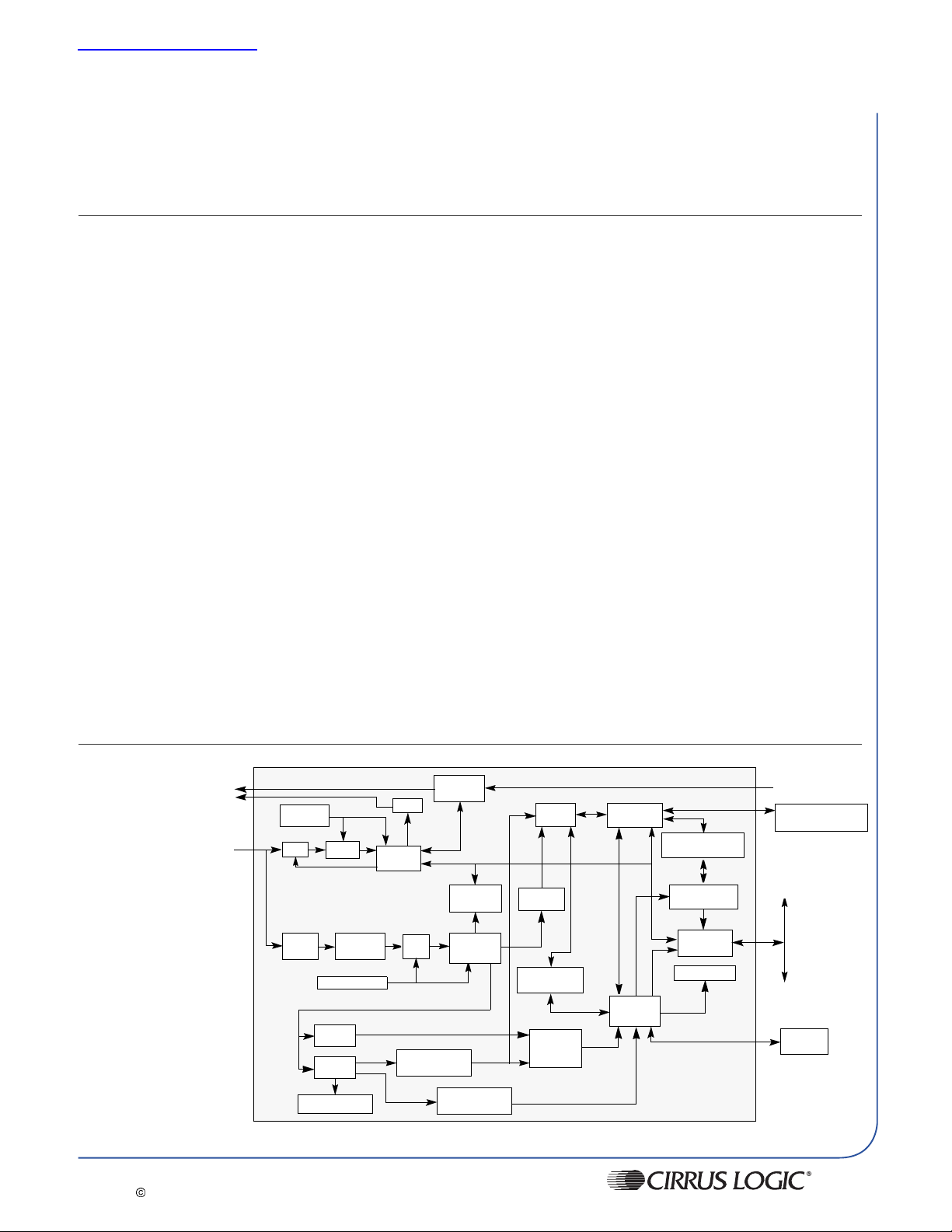
Block
Diagram
TO PO WE R
DRIVERS
FROM
IV AMP
SAMPLE
RATE GEN
VGA
SUM &
VGA
SUB-Q READ
ADCS
LOW PASS
FILTER
SYNTHE SIZER
8/16
DEMOD
EFM
DEMOD
SCP
DACS
RF
ADC
C1/C2 ECC &
DE-INTER LEAVE
SPINDLE
CONTROL
CHANNE L
QUALI TY
DPLL &
DATA CHNL
SUBCODE
DE-INTER LEAVE
DS588PP1 - rev 0.4 April 11, 2002 CONFIDENTIAL
Copyright 2002 Cirrus Logic Inc.
RAM
BAC
CAPTURE
LAYERED ECC
& DVD ECC
HEADER
SEARCH &
CHECKS
MICRO
INTERFACE
BUFFER
MANAGER
CSS
AUTHENTIFICATION
CSS
DESCRAMBLE
HOST
INTERFACE
NAVIGATION
CL-CS3712
www.cirrus.com
FROM
SENSORS
LOCAL
MICR OCONTRO LLER
ATAP I O R
MPEG
BUFFER
MEMORY

Features (Cont.)
PRELIMINARY DRAFT
RF Amp
• Provides laser power control
• Gain control in digital domain
• Generates focus error and tracking signal
• Provides RF signal for the data channel
• Bypass for external RF amp applications
Data Channel
• Digital PLL provides flexible control of center
frequency to support improved access times
• Channel quality provided for parametric calibration
• Channel data rates up to 210 Mbits/sec.
• Flexible and error-tolerant channel sync mark
windowing
SCP (Servo Control Processor)
• Includes a servo control processor for focus, tracking,
sled, and spindle servo loops
• Significantly faster capture for focus and tracking
• Effective in a wide range of parameter variations
• Superior response to defects, shock, and vibration
• Supports both CLV (constant linear velocity) and CAV
(constant angular velocity) modes
ECC
• Real-time DVD ECC error correction
• Real-time CD-ROM layered ECC error correction with
programmable number of sets of P-word and Q-word
corrections per sector (up to 64 total)
• C1/C2 ECC and de-interleaving
• Real-time subcode error correction in CD-DA
(compact disc digital audio) mode
Decoder
• Supports hardware streaming operation
• DVD navigation support
• Supports ADB (audio data buffering)
• Automatic target sector header search
• Hardware sector header validity check
• Supports high-speed Intel
microcontrollers
• Supports nonmultiplexed and multiplexed address
and data buses
- and Motorola-type
Host Interface
• True real-time hardware/software ATAPI compatibility
• Supports Ultra DMA: capable of synchronous DMA
data rates up to 33.3 Mbytes/sec.
• Supports ATA PIO modes 3 and 4 transfers without
IOCHRDY
Host Interface (cont.)
• Supports DMA modes 1 and 2
• Hardware implementation of:
- ATAPI packet command
- ATAPI reset command
High-Performance
• PIO/DMA ATAPI bus transfer rate:
- PIO modes 3 and 4, multiword DMA modes 1
and 2, and singleword DMA modes 1 and 2
• Data transfer rate:
- CD-ROM CLV –maximum 32 × data rate with
25% overspeed capture
- CD-ROM CAV – maximum 40× OD data rate
- DVD-ROM CLV – maximum 6× data rate with
33% overspeed capture
- DVD-ROM CAV – maximum 8× OD data rate
- DVD+R CLV – max. 4x read
• Buffer bandwidth:
- 55 Mbytes per second with 16-bit DRAM
Buffer Manager
• Dual-port circular buffer control with access-priority
resolver
• Supports streaming operation
• Direct addressing of up to 4 Mbytes of DRAM
• Supports variable buffer segmentation
• Programmable timing control for SDRAM
• Host overrun control
• Supports 16-bit SDRAM
Overview (Cont.)
The CL-CS3712 servo control processor implements the
focus, tracking, sled, and spindle servo loops. An ADC is
provided to convert the focus and tracking error signal.
The outputs to the power drivers are linear DACs.
The CL-CS3712 supports real-time DVD ECC, CD-ROM
C1/C2, and layered ECC correction, which is
programmable for up to 64 P- and Q-word corrections per
sector. It also supports subcode R/W correction in CDDA (compact disc digital audio) mode.
C ONFIDENTIAL DS588PP1 - rev 0.4 April 11, 2002
www.cirrus.com
The buffer manager controls the flow of data from the data
channel, through the ECC, and to either the host interface
or the serial audio channel. Data is stored and retrieved in
the external buffer memory using interleaved access
cycles. The buffer memory is implemented with SDRAM
devices. Up to 4 Mbytes of SDRAM can be directly
addressed by the CL-CS3712.
Copyright
2002 Cirrus Logic Inc.

Features (Cont.)
Microcontroller Interface
• Supports high-speed Intel- and Motorola-type
microcontrollers
• Supports nonmultiplexed and multiplexed address
and data busses
• Interrupt or polled microcontroller interface
• Microcontroller access to six external switch settings
on the buffer bus
- Three-level power-down capability when idle,
automatic power-up when command is
received
PRELIMINARY DRAFT
Overview (Cont.)
www.cirrus.com
C ONFIDENTIAL DS588PP1 - rev 0.4 April 11, 2002
Copyright
2002 Cirrus Logic Inc.

PRELIMINARY DRAFT
System Block Diagrams .........................................................................................................................1
Functional Decriptions............................................................................................................................2
Decoder.....................................................................................................................................2
Data Channel ............................................................................................................................4
Servo Channel...........................................................................................................................6
Register Map..........................................................................................................................................8
Pinout Information ...............................................................................................................................13
Pinout Diagram .......................................................................................................................13
Pin Decriptions ........................................................................................................................14
Package And Order Information...........................................................................................................19
Package Information ...............................................................................................................19
LQFP Ordering Information.....................................................................................................21
Table of Contents
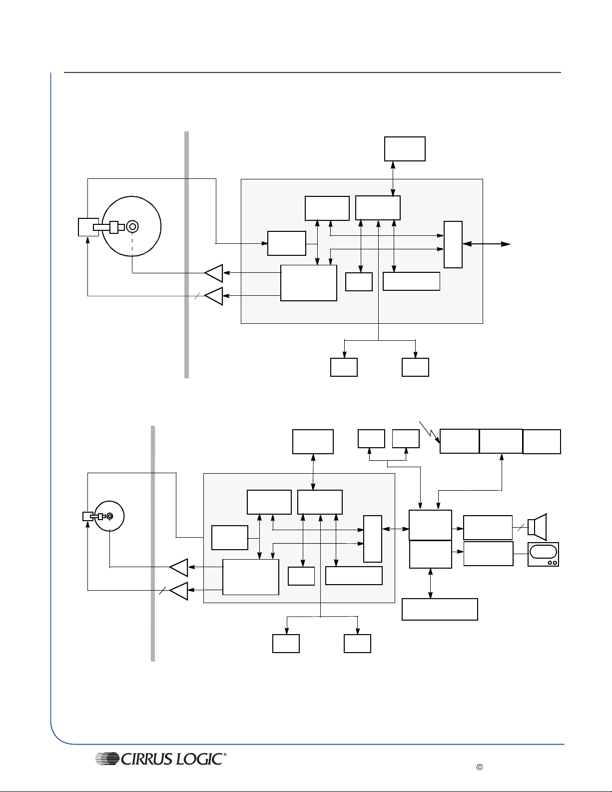
DVD-ROM ...................................................................................................................1
DVD PLAYER ..............................................................................................................1
DVD Mode....................................................................................................................2
CD Form .......................................................................................................................3
Pickup/Sensor Interface ...............................................................................................6
Servo Control Processor ..............................................................................................6
Servo DACs..................................................................................................................6
DS588PP1 - rev 0.4 April 11, 2002 C ONFIDENTIAL
Copyright 2002 Cirrus Logic Inc.
www.cirrus.com
iii
System Block Diagrams PRELIMINARY DRAFT
System Block Diagr ams
DVD-ROM
BUFFER
MEMORY
CL-CS3712
DATA
CHANNEL
DECODER
SLED/TRACK/FOCUS
DVD PLAYER
SPINDLE
SLED/TRACK/FOCUS
SPINDLE
3
POWER
DRIVERS
3
POWER
DRIVERS
CL-CS3712
RF AMP
CONTROL
PROCESSOR
CHANNEL
SERVO
RF AMP
DATA
SERVO
CONTROL
PROCESSOR
BUFFER
MEMORY
DECODER
CSS
CSS
ROM MC
DVD/CD-ROM
ECC
DVD/CD-ROM
ROM MC
ATAPI
ATAPI
ECC
IR
SENSOR
AC-3
AUDIO
DECODER
MPEG2
VIDEO
DECODER
BUFFER MEMORY
(2 MBYTES)
USER
CONTROL
6 CHANNEL
AUDIO
NTSC/PAL
ENCODER
HOST
INTERFACE
ATAPI
LED
DISPLAY
6
ROM MC
C ONFIDENTIAL DS588PP1 - rev 0.4 April 11, 2002
1
www.cirrus.com
Copyright
2002 Cirrus Logic Inc.

PRELIMINARY DRAFT
Functional Dec rip tions
This section overviews the main functional blocks of the CL-CS3712 Integrated AVI/
ATAPI DVD Drive Manager, and is divided into the following sub-sections:
• "Decoder" on page 2
• "Data Channel" on page 4
• "Servo Channel" on page 6
Decoder
The CL-CS3712 contains a highly automated DVD/CD decoder that takes EFM data from
the Analog Front and Digital PRML read channel and transform this data through a series
of operations into user data and sends it to the Host controller.
The sequence of operation is as follows:
The high level firmware sets up the decoder through the UP control interface. The
decoder is controlled through a register set. The high level FW sets up the mode of
operation (CD or DVD), the buffer manager and the host interface. The external SDRAM
buffer is controlled through a set of address pointers programmed by the FW. This
address pointers controls the data flow from the DISC, to and fro to the ECC Block and
the HOST.
Functional Decriptions
DVD Mode
The actual data that is written on the DVD DISC is a transformed version of the user data
and follows the DVD Physical Specification.
To understand the decoder flow the transformation process needs to be understood,
which is beyond the scope of this document. In summary the user data is organized in
sectors (2048 bytes). The transformation process involves adding ID (Sector #) and other
information such as copy protection etc. to the data, Scrambling the data, ECC encoding,
splitting the data into recording frames , EFM modulation and creation of EFMP frames
with unique sync patterns inserted for EFMP frame identification.
The function of the decoder is to take this transformed data and convert back into the
user format.
Once the FW sets the start transfer control bit(s) in the decoder, the Decoder starts
processing the data from the Read Channel. The data is in the EFMP format (Eight to
Fourteen Modulation Plus) as defined in the DVD Physical Specification. The first step is
to synchronize and align the data on the EFMP frame boundaries by detecting unique
sync patterns that are embedded in the EFMP data stream. Once the data is aligned on
the EFMP frame boundary it is de-serialized into 16-bit symbols, and than demodulated
into 8 bits of data according to the EFMP modulation standard.
The next step is to determine the right starting point to start the transfer of data into the
buffer. The FW will program the Target Header or ID information. Once the incoming data
ID matches the programmed ID, data transfer to the Buffer starts. The data transfer
DS588PP1 - rev 0.4 April 11, 2002 CONFIDENTIAL
Copyright 2002 Cirrus Logic Inc.
www.cirrus.com
2

Functional Decriptions PRELIMINARY DRAFT
always start on an ECC boundary. The HW monitors the subsequent ID to detect any
interruption in the DVD data stream.
After sufficient data is stored (at least 1 ECC Block = 16 sectors) in the Buffer, the Error
Correction (ECC) system can start the Error Detection and Correction. The Error
Correction algorithm is programmable to allow for multi-pass correction, depending
upon the application e.g. in the DVD-ROM case, one would program it with more passes
than for DVD-Movie case.
Once ECC system has corrected one ECC block, this data can be transferred to the
host. However before transferring this data need to be de-scrambled. The descrambling process is done during Host transfer to save Buffer BW.
All the Disc Transfer, ECC correction, Descrambling and Host Transfers are done in
parallel without any intervention from the micro-controller. The hardware keeps track of
how many sectors are transferred from the disc to the buffer, how many sectors have
been corrected and how many transferred to the host. This is a fully automated
operation also known as "full streaming".
CD Form
The actual data that is written on the CD DISC is a transformed version of the user data
and follows the CD Physical Specification. The Physical format of a CD disc is defined
by the CD-Digital Audio Physical Specification. All CD whether CD-ROM or CD-Audio
follows this standard. The recordable formats also follow this format, except for the
linking area for multi-session recordings.
Again it is beyond the scope of this document to describe the CD formats as unlike the
DVD format, there are host of different formats that the decoder needs to process.
These are CD-DA, CD-ROM Mode 0, CD-ROM Mode 2/Form1 CD-ROM Mode 2/ Form
2 plus CD-Recordable data. In addition for the CD-DA mode the decoder needs to
process the Sub Channel Data. The Sub-Channel contains additional information that is
embedded in the EFM data stream, which contains sector identifications and other
information unique to the data.
Basically there are two types of data, CD-Audio and CD-ROM (with different modes and
form). For CD-Audio both the main channel and the Sub Channel Data needs to be
processed, for the CD-ROM case only the main channel data is processed.
The data arriving from the Read Channel is in the EFM format, first it is synchronized
and aligned on the EFM frame boundaries. After synchronization the data is
demodulated using the EFM demodulation table.
CD data is protected through 2 levels of correction C1 and C2 for the CD-DA and 3
levels C1, C2 and C3 for CD-ROM formats.
C1 and C2 correction is done on the fly, i.e. before the data is transferred to the Buffer.
After EFM demodulation, the data is sent to CIRC block (Cross Interleaved Reed
Solomon Code) which performs C1 and C2 correction on the incoming data. It also
marks data it cannot correct, these markers called C2 Pointers are used by the Audio
Interpolator block to perform audio interpolation and in the case of CD-ROM data, help
the C3 correction engine in identifying the errors quickly.
After the EFM demodulation, the Target Header Search looks for the target sector ID in
the data stream. In the case of CD-DA this ID is in the sub channel data stream,
C ONFIDENTIAL DS588PP1 - rev 0.4 April 11, 2002
3
www.cirrus.com
Copyright
2002 Cirrus Logic Inc.
PRELIMINARY DRAFT
whereas in the case of CD-ROM data it is embedded in the main channel data. Once the
Target Header is found the data transfer to the Buffer starts and the de-scrambling is
done while storing the data in the buffer from the disc. This data is than transferred to the
Host (ATAPI or Audio DAC interface)
In the case of CD-ROM data, depending on the format additional C3 correction needs to
be performed. This flow is similar to the DVD case, i.e. when sufficient sectors are
available in the buffer, the ECC engine starts correcting the data and the Host transfer
starts as soon as sufficient sectors are available after C3 correction.
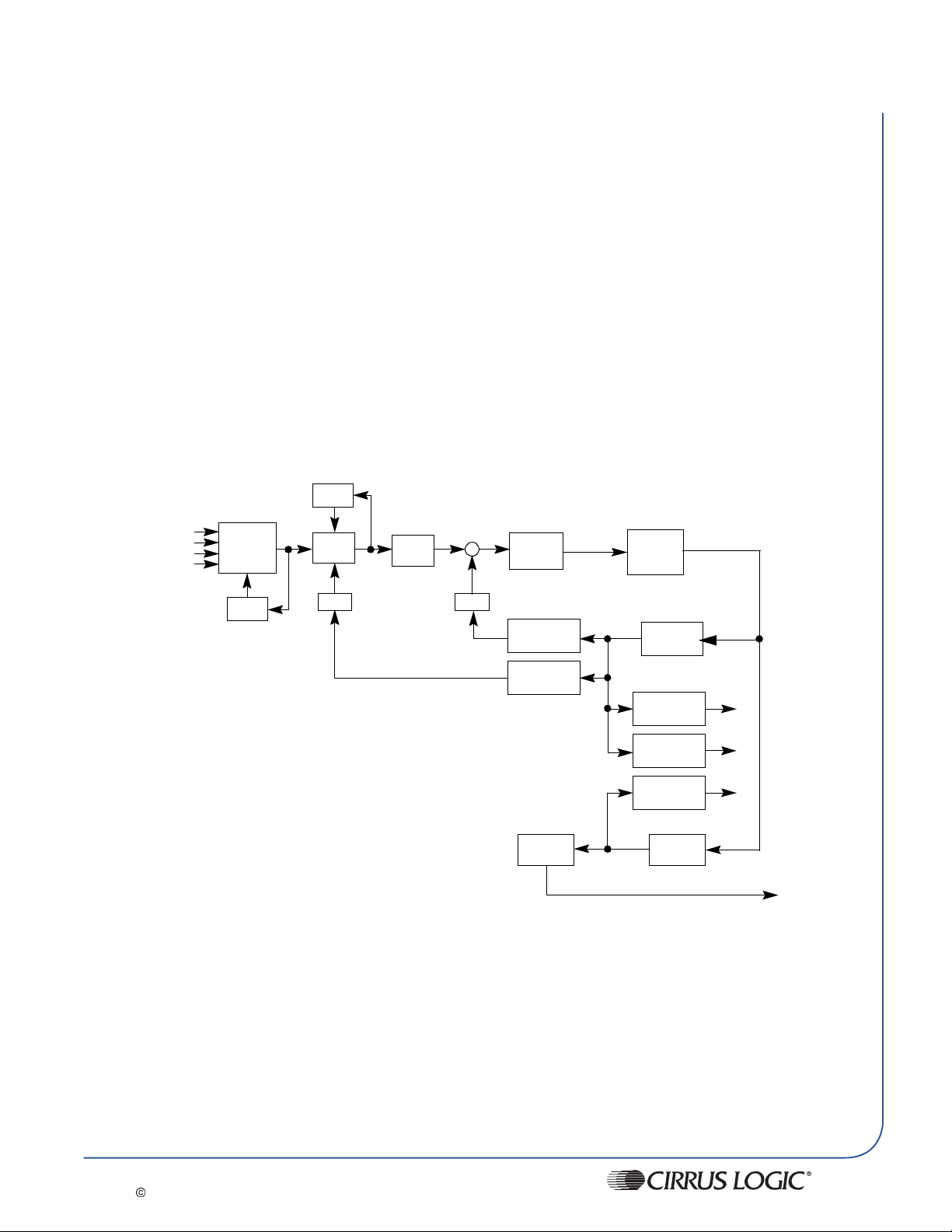
Data Channel
The CL-CS3712 contains a partial response maximum likelihood (PRML) read channel.
The channel takes the analog signals from the optical pickup's (OPU) photo detector
outputs, detects the EFM or EFM+ data, and sends the data to the decoder. Figure 1
illustrates the Data Channel architecture.
OFFSET
CONTROL
Functional Decriptions
PD A
PD B
PD C
PD D
ATTENUATOR
AND
SUMMATION
OFFSET
CONTROL
VGA
DAC
LPF
+
DAC
Figure 1. Data Channel Diagram
RF ADC
OFFSET
CONTROL
GAIN
CONTROL
SEQUENCE
DETECT OR
DIGIT AL
EQUALIZER
ENVELOPE
DETECT
DEFECT
DETECT
RF TRACK
CROSSING
CHANNEL
QUALI TY
ITR
TO DECODER
DS588PP1 - rev 0.4 April 11, 2002 CONFIDENTIAL
Copyright 2002 Cirrus Logic Inc.
www.cirrus.com
4

Functional Decriptions PRELIMINARY DRAFT
The CL-CS3712 data channel architecture minimizes analog signal processing and
migrates all feasible functionality to real-time digital signal processing blocks. The
analog blocks are:
• Summation Amplifier
• Digitally Controlled Variable Gain Amplifier (VGA)
• Analog Low Pass Filter (LPF)
• Analog-to-Digital Converter (RF ADC)
The main data path digital blocks are:
• Digital Equalizer
• Interpolate Timing Recovery (ITR)
• Sequence Detector
The data path blocks are supported by the loop control blocks: the digital automatic gain
control (DAGC), offset control, and digital asymmetry control. The digital defect detect
block allows the loops and the servo processor to coast through defects. u-Controller
accessible channel quality metrics support servo error signal gain and offset calibration.
The Attenuator and Summation block interfaces the OPU's A, B, C, and D photodetector
outputs or the RF signal to the data channel. The attenuator and offset loop keeps the
signals within the linear range of the circuitry. The channel can use either internally or
externally summed RF.
The variable gain amplifier (VGA) is part of the automatic gain control (AGC) loop. This
amplifier's gain is exponentially proportional to its gain control. The analog low pass filter
is designed to limit noise and serve as an anti-aliasing filter.
The CL-CS3712 contains a high speed analog to digtial convertor that allows the
majority of the signal processing to be performed in the digital domain. The sampling
frequency is fixed and can be Fsynth/2 or Fsynth/4. This allows for a wide range of
allowable input data rates.
The digital equalizer is a 5 tap finite impulse response filter. It's coefficients change
automatically as the data rate changes. The envelope detector is used to generate error
signals for the offset and AGC loops. The defect detection is also performed here. The
digital offset loop keeps the read signal's baseline at the ADC's range center. The AGC
also keeps the signal's amplitude within the ADC's range. These loops are digital with
the exception of the digital to analog convertors (DACs), ADC, an adder, and a VGA.
The CL-CS3712 data channel performs data separation via the ITR. This all digital
implementation of a phase locked-loop (PLL) makes for consistent chip to chip
performance. It also allows for wide capture ranges. This decreases the speed of seeks
in constant linear velocity (CLV) mode. It has been designed handle the rate changes
inherent in constant angular velocity (CAV) mode automatically. Asymmetry
compensation is performed at the ITR input.
The CL-CS3712 contains a maximum likelihood sequence detector especially designed
for low resolution DVD signals. This sequence detector achieves substantial signal
processing gain over a slicer detector.
C ONFIDENTIAL DS588PP1 - rev 0.4 April 11, 2002
5
www.cirrus.com
Copyright
2002 Cirrus Logic Inc.

PRELIMINARY DRAFT
The channel is controlled by a state machine that automatically starts timing recovery and
deals with defects. This ensures quick recovery from defects and fast data acquisition
after seeks.
The CL-CS3712 contains a versatile digital block that can be used to monitor the ongoing
‘health’ or ‘quality’ of the channel, and that enables accurate equalization calibration to
compensate for wide variations in disc resolution.
Servo Channel
The CL-CS3712 contains an integrated servo system that can control either a CDROM or
a DVD mechanism, with the following features:
Functional Decriptions
• Servo Control Processor (SCP), implementing algorithms designed specifically
for optical disc drives
• Supports dual pick up for CD and DVD applications
• Integrated RF amplifier with Laser Diode Automatic Power Control (LD APC)
• Track counter with velocity estimation
Figure 2 shows the CL-CS3712 in a complete servo system. Four control loops can be
processed by this chip: focus, track, sled, spindle. Since the CL-CS3712 contains a
processor, control algorithms and interface circuitry, little external hardware and little
microcontroller intervention is required to implement the servo system.
Pickup/Sensor Interface
The Pickup Interface is the input to the servo control processor (SCP). This circuitry
provides the analog and digital processing needed before the SCP can process the
control signals from the sensors. Since laser diode automatic power control and
reference voltage generation are also provided, the CL-CS3712 can be connected
directly to the pick up electronics without the need for an external RF amplifier.
Servo Control Processor
The SCP does all the processing necessary to control all four servo loops with little
loading of the external microcontroller. The microcontroller sends setup information and
commands to the control system through the microcontroller interface. It can also monitor
key metrics and change control variables to optimize system performance.
• Multi-function register banks
• External microcontroller interface circuitry
• Programmable Sample Rate Subsystem
All parameter variables and SCP instructions are stored in internal RAM. Since the CLCS3712 is a RAM based device, the microcontroller must first initialize these RAMs
before servo operations can begin.
Servo DACs
Control outputs for the sled, focus, and track loops are converted to analog through an
array of three 11-bit DACs. The spindle loop has a pulse width modulated (PWM) output.
DS588PP1 - rev 0.4 April 11, 2002 CONFIDENTIAL
Copyright 2002 Cirrus Logic Inc.
www.cirrus.com
6

Functional Decriptions PRELIMINARY DRAFT
PICK UP
ELECTRONICS
PD OUTPUTS
10
VREF1
LD-MON1
LD-PC1
LD-MON2
LD-PC2
PICK UP
INTERFACE
SERVO SYSTEM
MICROCONTROLLER
MICROCONTROLLER
SPIN
TRANSDUCER
SERVO
CONTROL
PROCESSOR
(SCP)
INTERFACE
SPINDLE
MOTOR
SLED
MOTOR
SERVO
DACS
POWER AMPS
DAC
OUTPUTS
4
VREF2
PWM-SP
MOTION
Figure 2. Servo System Diagram
FOCUS
ACTUATOR
TR A CK I N G
ACTUATOR
C ONFIDENTIAL DS588PP1 - rev 0.4 April 11, 2002
7
www.cirrus.com
Copyright
2002 Cirrus Logic Inc.

PRELIMINARY DRAFT
Register Map
Address (Hex) Register Name R/W
30H-31H Audio Address Pointer (AAP) R/W
34H-35H Host Address Pointer (HAP) R/W
Register Map
Table 1: CL-CS3712 Registers
00H ATAPI Error (ATERR) R/W
01H ATAPI Features (ATFEA) R/W
02H ATAPI Interrupt Reason (ATINT) R/W
03H ATA Sector Number (ATSECN) R/W
04H ATAPI Byte Count Low (ATBCL) R/W
05H ATAPI Byte Count High (ATBCH) R/W
06H ATAPI Drive Select (ATDSEL) R/W
07H ATAPI Command (ATCMD) R
08H ATAPI Packet (ATPKT) R
09H Alternate ATAPI Error (ALTERR) R/W
0AH ATA Drive Control/Status (ATDRV) R/W
0BH Host Drive Address (HDA) R/W
0CH AT Control 1 (ATCTRL1) R/W
0DH AT Control 2 (ATCTRL2) R/W
0EH AT Control 3 (ATCTRL3) R/W
10H Host Interrupt Status 1 (HIST1) R/W
11H Host Interrupt Enable 1 (HIEN1) R/W
12H Host Interrupt Status 2 (HIST2) R/W
13H Host Interrupt Enable 2 (HIEN2) R/W
15H PC Mode Control 1 (PCMODE1) R/W
16H Host Transfer/Packet FIFO Control (HXFR) R/W
17H ATAPI Phase Lock Release (ATULOCK) W
18H Synchronous DMA Control (SDMA) R/W
19H PC Mode Control 2 (PCMODE2) R/W
1BH MPEG Interface Configuration 1 (MPEGCFG1) R/W
1CH MPEG Interface Configuration 2 (MPEGCFG2) R/W
1DH MPEG Interface Configuration 3 (MPEGCFG3) R/W
1EH MPEG/BCA Interface Interrupt Status (MPEGIST) R/W
1FH MPEG/BCA Interface Interrupt Enable (MPEGIEN) R/W
2CH C2P Threshold Control (C2PTC) R/W
2DH C2P Threshold Counter R/W
2EH Servo Coefficient Control R/W
2FH DAC Interface Status/Control (DACS) R/W
DS588PP1 - rev 0.4 April 11, 2002 CONFIDENTIAL
Copyright 2002 Cirrus Logic Inc.
www.cirrus.com
8

Register Map PRELIMINARY DRAFT
Table 1: CL-CS3712 Registers
Address (Hex) Register Name R/W
38H-39H Host Buffer Start Address (HBSA) R/W
3CH-3DH Local Address Base Pointer (LABP) R/W
40H-41H Host Buffer End Address (HBEA) R/W
44H-45H Host Transfer Count (HTC) R/W
46H Scheduled Buffer Data Access (SBDA) R/W
47H Buffer Transfer Control (BTC) R/W
48H-49H Adjust Difference Block Count (ADBC) R/W
4AH Host Transfer Sector Type (HTST) R/W
4BH Host Transfer Format 1 (HTF1) R/W
4CH Host Transfer Format 2 (HTF2) R/W
4DH Buffer Timing Control (BTIM) R/W
4EH Buffer Mode Control (BMC) R/W
4FH DRAM Refresh Period (RFSH) R/W
50H-51H Disc Address Pointer (DAP) R/W
54H-55H Disc Buffer Start Address (DBSA) R/W
58H-5BH Disc Transfer Count (DTC) R/W
5CH-5DH Disc Buffer End Address (DBEA) R/W
60H-61H Corrector Address Pointer (CAP) R/W
64H-65H Sector to be Corrected (STC) R/W
66H-67H Current Host Transfer Count (CHTC) R
68H-6BH Corrector Transfer Count (CTC) R/W
70H-71H Buffer Sector Size (BSS) R/W
72H-73H Difference Block Count (DBC) R/W
74H-77H Local Address Offset Pointer (LAOP) R/W
78H-79H Navigation Pack Address Pointer (NAP) R
7AH-7BH Navigation Pack Detected (NAVPKDET) R
7CH Navigation Play Control (NAVCTL) R/W
7FH Threshold Transfer Count (TTC) R/W
80H Decoder Operation Mode (DOPMD) R/W
81H Disc Configuration (DCFG) R/W
82H Disc Transfer Control/Status (DCTRL) R/W
83H ECC Control/Status 1 (ECC1) R/W
84H DVD ECC Error Information (ECC2) R/W
85H Data Channel Interface Configuration 2 (DCCFG2) R/W
86H Target Header (TRGHD) R/W
87H Target Header Search Time-Out (HSTO) R/W
88H RAW Header/Subheader Read-Out (RHDRD) R
89H RAW Header Mismatch Threshold (RHDMTH) R/W
8BH Expected Header Read-Out (EXPHD) R
C ONFIDENTIAL DS588PP1 - rev 0.4 April 11, 2002
9
www.cirrus.com
Copyright
2002 Cirrus Logic Inc.

PRELIMINARY DRAFT
Address (Hex) Register Name R/W
8CH RAW Header/SubHeader Flag (HDFLG) R
8DH Header Read-Out Control (RDCTRL) R/W
8EH Data Channel Interface Configuration 3 (DCCFG3) R/W
90H Disc Interrupt Status 1 (DIST1) R/W
91H Disc Interrupt Enable 1 (DIEN1) R/W
92H Disc Interrupt Status 2 (DIST2) R/W
93H Disc Interrupt Enable 2 (DIEN2) R/W
94H Disc Transfer Control 1 (DCTRL1) R/W
95H Sector Per Track Count (SPTC) R/W
98H BCA Control 1 R/W
99H BCA Status 1 R/W
9AH BCA Control 2 R/W
9BH BCA Control 3 R/W
9CH BCA Control 4 R/W
9DH BCA Channel Clock R/W
9EH-9FH Spindle Speed R
A0H Defect Address FIFO1/FIFO2(DMF) R/W
A1H C1/C2 Control (C12CNTL) R/W
A2H EFM Sync Control (EFMSYCTL) R/W
A3H EFM Plus Sync Control (EFMPSYCTL) R/W
A4H Subcode Read-Out (SBRD) R
A5H Subcode Control/Status (SBCTL) R/W
A6H EFM Plus Sync Status (EFMPSYNSTS) R
A7H Corrected ID Read-Out (CIDR) R/W
B5H SRAM Diagnostics Status 1 (SRAMST1) R
B6H SRAM Diagnostics Status 2 (SRAMST2) R
B7H SRAM Diagnostics Status 3 (SRAMST3) R
B8H SRAM Diagnostics Control 1 (SRAMDIACTL1) R/W
B9H SRAM Diagnostics Control 2 (SRAMDIACTL2) R/W
BAH SRAM uC Access Data (SRAMUPDATA) R/W
BBH SRAM uC Access Address (SRAMUPADDR) R/W
BDH Test1 (TEST) R/W
BEH Product and Revision Number (PRVN) R
BFH Miscellaneous Control (MISC) R/W
C0H Power Control R/W
C1H Clock Selection R/W
C2H RF ADC Diagnostic Control 1 R/W
C3H RF ADC Diagnostic Control 2 R/W
C4H Analog Diagnostic R/W
Register Map
Table 1: CL-CS3712 Registers
DS588PP1 - rev 0.4 April 11, 2002 CONFIDENTIAL
Copyright 2002 Cirrus Logic Inc.
www.cirrus.com
10

Register Map PRELIMINARY DRAFT
Table 1: CL-CS3712 Registers
Address (Hex) Register Name R/W
C5H-C7H RF ADC Diagnostic Accumulator R
C8H Laser Diode 1 Control R/W
C9H Laser Diode 2 Control R/W
CAH Reference Voltage/Diode/RF Amp Configuration R/W
CBH Pickup Interface R/W
CCH Analog Static Data Channel VGA R/W
CDH Analog Static Data Channel LPF R/W
CEH RF ADC Calibration Control R/W
CFH Bandgap Reference Calibration Control R/W
D0H Moving-Average Filter/Digital Filtering 1 R/W
D1H Digital Filtering 2 R/W
D2H Zone Control R/W
D3H Offset Loop Control R/W
D4H Automatic Gain Control R/W
D5H Gain Loop Accumulator Layer 0 and Layer 1 R/W
D7H Offset Loop Accumulator Layer 0 and Layer 1 R/W
D8H RF Envelope Detector Read R/W
D9H LF Envelope Detector R/W
DAH Topstate Monitor R/W
DBH Asymmetry Accumulator Layer 0 and Layer 1 R/W
DCH Asymmetry Control R/W
DDH Channel Top Level State Control 1 R/W
DEH Channel Top Level State Control 2 R/W
DFH Channel Top Level State Control 3 R/W
E0H DPLL Control 1 R/W
E1H DPLL Control 2 R/W
E2H DPLL Control 3 R/W
E3H Sequence Detector R/W
E4H-E5H DPLL Center Period Accumulator R/W
E6H-E7H Channel Quality Accumulator R
E8H Channel Quality Mode Select R/W
E9H Defect Control 1 R/W
EAH Defect Control 2 R/W
EBH Defect Control 3 R/W
ECH RF BCA Slicer R/W
EDH RF BCA Parser R/W
EFH Digital Diagnostic R/W
F0H Track Crossing Control R/W
F1H Servo Control R/W
11
www.cirrus.com
C ONFIDENTIAL DS588PP1 - rev 0.4 April 11, 2002
Copyright
2002 Cirrus Logic Inc.

PRELIMINARY DRAFT
Address (Hex) Register Name R/W
F2H SCP Program Command (SPC) R/W
FBH SCP State Generator M Divider R/W
FCH SCP State Generator N/P Dividers R/W
FDH Memory Data R/W
FEH-FFH SCP Memory Control/Address R/W
Register Map
Table 1: CL-CS3712 Registers
DS588PP1 - rev 0.4 April 11, 2002 CONFIDENTIAL
Copyright 2002 Cirrus Logic Inc.
www.cirrus.com
12

Pinout Information PRELIMINARY DRAFT
Pinout Informati on
Pinout Diagram
AGND
NC_GND
AGND
REXT
AVDD
NC_GND
LD-MON2
LD-PC2
VREF1
AGND
AVDD
PD-CF
HP_FILT2
RF_N
RF_P
PD-CB
PD-CA
PD-CE
PD-CC
PD-CD
NC_GND
PD-T
HP_FILT3
PD-DB
PD-DD
PD-DC
PD-DA
HP_FILT1
LD-MON1
LD-PC1
PD-DF2
PD-DF1
PD-DE2
PD-DE1
AGND
AVDD
APC_GND
DAC-F
DAC-T
ADC-AUX
AVDD
VREF2
NC_GND
DAC-SL
DAC-TL
NC_GND
AVDD
NC_GND
AGND
PWM-SP
SPIN_P
SPIN_N
157
159
158
160
161
162
164
163
165
166
167
169
168
170
171
172
174
173
175
176
177
179
178
180
181
182
184
183
185
186
187
189
188
190
191
192
194
193
195
196
197
198
199
200
201
203
202
204
205
206
208
207
AVD D
CKE
WE*
BVDD
CS0*
CS1*
CAS*
RAS*
BD15
BD14
BD13
BD12
BVDD
BD11
BD10
BVDD
BA11
BA10
BA9
BA8
BA7
BA6
BA5
BA4
BVDD
BA3
1
2
3
4
5
6
7
8
9
10
11
12
13
14
15
16
17
18
19
20
21
22
23
24
25
26
27
28
29
30
31
32
33
34
35
36
37
38
39
40
41
42
43
44
45
46
47
48
49
50
51
52
CL-CS3712
208-Pin LQFP
156
155
154
153
152
151
150
149
148
147
146
145
144
143
142
141
140
139
138
137
136
135
134
133
132
131
130
129
128
127
126
125
124
123
122
121
120
119
118
117
116
115
114
113
112
111
110
109
108
107
106
105
NC
NC
NC
NC
NC
AV DD
XTALO
MCLK2/XTALI
AGND
BGND
MCLK1
CLK_OUT
uC_CLK
CGND
DMA33CLK
RST*
INT1
INT2
BGND
CS*
WR*/R/W*
RD*/DS
A7/ALE
A6
A5
A4
BVDD
A3
CGND
A2
A1
A0
CVDD
AD7
BGND
AD6
AD5
AD4
AD3
AD2
AD1
AD0
EF2
BVDD
EF1
BGND
N/C
N/C
EXTCR
N/C
TEST
TEST_ENBL*
DIAG4
DIAG3
DIAG2
DIAG1
RF_ENV
CH QUAL MON
AGND
BGND
SDCLK
DQMU
DQML
BGND
CVDD
CGND
BD9/PLL_CLK_BP_SL
BD8/CS_P OLARITY
BD7/MOT-I*
BD5/DEC_CLK_BP_SL
BD6/M-NM*
BD4/DTSL
BD3/XTSL
BGND
BD2/UCSL2
BD1/UCSL1
BD0/UCSL0
BGND
13
www.cirrus.com
5354555657585960616263646566676869707172737475767778798081828384858687888990919293949596979899
DA1
DA0
BA2
BA1
BA0
DD7
DD8
DD6
DD9
DD5
DD4
DD3
DD10
DD11
BGND
CVDD
CGND
HRESET*
BVDD
BGND
DD12
DD2
DD1
DD0
DD14
DD13
BVDD
DD15
BGND
DIOW*
DMARQ
BVDD
DIOR*
BGND
IORDY
INTRQ
IOCS16*
DMACK*
DA2
BVDD
BGND
CGND
PDIAG*
DASP*
CS1FX*
CS3FX*
C ONFIDENTIAL DS588PP1 - rev 0.4 April 11, 2002
Copyright
100
101
102
103
104
N/C
N/C
N/C
CVDD
BGND
EXTCQ
2002 Cirrus Logic Inc.

PRELIMINARY DRAFT
Pin Decriptions
Abbreviation or Conv ention Description
Pin name in italics
Pinout Information
Table 2: Pin Map Legend
I A pin that functions as an input only.
O A pin that functions as an output only.
I/O A pin that operates as an input or an output.
OD An open-drain output.
TS A test pin.
Z A tristate output or input/output.
(*) Following a signal name designates an active-low signal.
An italicized function name for a multifunction pin indicates that the function is
only valid on the low-to-high transition of RST*.
Table 3: CL-CS3712 Pin Map
Type Name Pin(s) I/O Function
I/O-TS
I/O-TS
I/O-TS
I/O-TS
I/O-TS
I/O-TS
I/O-TS
I/O-TS
I/O-TS
I/O-TS
I/O-TS
I/O-TS
I/O-TS
I/O-TS
I/O-TS
I/O-TS
I
I
I
Host Data Bus
Host Address Lines
Host
Interface
Signals
DD15
DD14
DD13
DD12
DD11
DD10
DD9
DD8
DD7
DD6
DD5
DD4
DD3
DD2
DD1
DD0
DA2
DA1
DA0
CS1FX* 95 I Host Chip Select 0*
CS3FX* 96 I Host Chip Select 1*
DIOR* 82 I Host I/O Read Strobe*
DIOW* 81 I Host I/O Write Strobe*
HRESET* 57 I Host Reset*
IOCS16* 88 OD 16-bit Data Transfer*
INTRQ 87 O -TS Host Interrupt Request
IORDY 83 O -TS I/O Channel Ready
79
77
74
71
69
67
63
60
58
62
65
68
70
72
76
78
94
89
92
DS588PP1 - rev 0.4 April 11, 2002 CONFIDENTIAL
Copyright 2002 Cirrus Logic Inc.
www.cirrus.com
14

Pinout Information PRELIMINARY DRAFT
Table 3: CL-CS3712 Pin Map (Continued)
Type Name Pin(s) I/O Function
DMARQ 80 O -TS DMA Request
Host
Interface
Signals (cont.)
Buffer
Interface
Signals
DMACK* 85 I DMA Acknowledge*
PDIAG* 90 I/O Passed Diagnostics*
DASP* 98 I/O Slave Present
SDCLK 10 O SDRAM CLK
CKE 11 O Clock Enable
DQMU 12 O Upper Data Mask Enable
DQML 13 O Lower Data Mask Enable
WE* 15 O Write Enable
CS0* 17 O Chip Select 0
CS1* 18 O Chip Select 1
CAS* 19 O Column Address Strobe Low
RAS* 20 O Row Address Strobe
BA11
BA10
BA9
BA8
BA7
BA6
BA5
BA4
BA3
BA2
BA1
BA0
BD15
BD14
BD13
BD12
BD11
BD10
BD9/
PLL_CLK_BP_SL
BD8/CS_POLARITY 31 I/O Buffer Data Bus Bit 8 / uComputer Clock Select
BD7/MOT-I* 32 I/O Buffer Data Bus Bit 7 / Motorola-Intel
BD6/M-NM* 33 I/O Buffer Data Bus Bit 6 / Multiplexed - Nonmultiplexed
BD5/
DEC_CLK_BP_SL
BD4/DTSL 35 I/O Buffer Data Bus Bit 4 / Drive Test Select
BD3/XTSL 36 I/O Buffer Data Bus Bit3 / XTAL Select
BD2/UCSL2
BD1/UCSL1
BD0/UCSL0
42
43
44
45
46
47
48
50
52
53
54
55
21
22
23
24
27
29
30 I/O Buffer Data Bus Bit 9 / PLL Clock Bypass
34 I/O Buffer Data Bus Bit 5 / Decoder Clock
38
40
41
O
O
O
O
O
O
O
O
O
O
O
O
I/O
I/O
I/O
I/O
I/O
I/O
I/O Buffer Data Bus Bit 2-0 / uComputer Clock Select
Buffer Address [11:0]
Buffer Data Bus
15
www.cirrus.com
C ONFIDENTIAL DS588PP1 - rev 0.4 April 11, 2002
Copyright
2002 Cirrus Logic Inc.

PRELIMINARY DRAFT
Table 3: CL-CS3712 Pin Map (Continued)
Type Name Pin(s) I/O Function
Pinout Information
Microcontroller
Interface
Signals
Servo
Analog
Interface
Signals
Clock
Interface
Signals
AD7
AD6
AD5
AD4
AD3
AD2
AD1
AD0
A7/ALE 134 I
A6
A5
A4
A3
A2
A1
A0
CS* 137 I Chip Select*
RD*/DS 135 I Read Strobe*/data Strobe
WR*/ R/W* 136 I Write Strobe/ Read/write*
INT1 140 O-OD Interrupt1
INT2 139 O-OD Interrupt2
RST* 141 I Reset*
SPIN_P
SPIN_N
DAC-TL 164 O Tilt DAC
DAC-SL 165 O Sled DAC
DAC-F 171 O Focus DAC
DAC-T 170 O Tracking DAC
ADC-AUX 169 I Auxiliary ADC
PWM-SP 159 O Spin PWM
EXTCR 108 I
EXTCQ 102 I
VREF2 167 O Voltage Reference 2
MCLK1 146 I Master Clock 1
MCLK2/XTALI 149 I Master Clock 2 / Crystal Input
XTALO 150 O Crystal Output
DMA33CLK 142 I DMA33 Clock
CLK_OUT 145 O Clock Output
uC_CLK 144 O Microcontroller Clock
123
121
120
119
118
117
116
115
133
132
131
129
127
126
125
158
157
I/O
I/O
I/O
I/O
I/O
I/O
I/O
I/O
Local Microcontroller Address And Data Bus
Local Microcontroller Address Bus Bit 5 /
Address Latch Enable
I
I
I
I
I
I
I
I
I
External Track Counter Real And External Track Counter
Local Microcontroller Address Bus
Spin Transducer
Quadrature
DS588PP1 - rev 0.4 April 11, 2002 CONFIDENTIAL
Copyright 2002 Cirrus Logic Inc.
www.cirrus.com
16

Pinout Information PRELIMINARY DRAFT
Table 3: CL-CS3712 Pin Map (Continued)
Type Name Pin(s) I/O Function
RF
Amplifier
Interface
Signals
Diagnostic
Signals
PD-DE1
PD-DE2
PD-DF1
PD-DF2
PD-DA
PD-DC
PD-DD
PD-DB
RF_P
RF_N
PD-CA
PD-CB
PD-CC
PD-CD
PD-CE
PD-CF
PD-T 187 I Photo Detector-T
LD-PC1
LD-PC2
LD-MON1
LD-MON2
VREF1 200 I/O Voltage Reference 1
REXT 205 I/O External Resistor
HP_FILT1
HP_FILT2
HP_FILT3
DIAG1
DIAG2
DIAG3
DIAG4
RF_ENV 5 O RF Envelope
CH QUAL MON 6 O Channel Quality Monitor
EF2
EF1
TEST_ENBL* 105 I Test Enable
TEST 106 I Test
175
176
177
178
182
183
184
185
194
195
192
193
190
189
191
197
179
201
180
202
181
196
186
4
3
2
1
114
112
O
O
I/O
I/O
I/O
I/O
O
O
I
I
I
I
I
I
I
I
I
I
I
I
I
I
I
I
I
I
I
I
I
Servo Differential Push Pull Amp Inputs
Photo Detector-DVD
RF External Summation Inputs
Photo Detector-CDROM
Photo Detector E & F-CDROM
Laser Diode Power Control
Laser Diode Monitor
High Pass Filter
Diagnostic 1-4
Error Flag (2:1)
17
www.cirrus.com
C ONFIDENTIAL DS588PP1 - rev 0.4 April 11, 2002
Copyright
2002 Cirrus Logic Inc.

PRELIMINARY DRAFT
Table 3: CL-CS3712 Pin Map (Continued)
Type Name Pin(s) I/O Function
8 , 151, 162,
Power
and
Ground
Pins
AVDD
AGND
BVDD
BGND
CVDD 26 , 61 , 99, 124 – Core Power Supply
CGND
APC_GND 172 – Apc Ground
NC_GND
168, 173, 198,
204
7, 148, 160,
174, 199, 206,
208
16, 25, 39, 51,
66, 73, 86, 91,
113, 130
9, 14, 37, 49,
56, 64, 75, 84,
93, 104, 111,
122, 138, 147
28, 59, 97, 128,
143
161, 163, 166,
188, 203, 207
– Analog Power Supply
– Analog Ground
– Buffer Power Supply
– Buffer Ground
– Core Ground
– Nc Ground
Pinout Information
DS588PP1 - rev 0.4 April 11, 2002 CONFIDENTIAL
Copyright 2002 Cirrus Logic Inc.
www.cirrus.com
18

Package And Order Information PRELIMINARY DRAFT
Package And Order Information
Package Information
For complete dimensional and thermal information, see the latest version of the Cirrus
Logic Package Information Guide. The package and PCB design affects the amount of
power that can be dissipated by the package and could limit the maximum transfer rate.
29.60 (1.165)
30.40 (1.197)
27.80 (1.094)
28.20 (1.110)
0.17 (0.007)
0.27 (0.011)
29.60 (1.165)
30.40 (1.197)
0.50
(0.0197)
BSC
0.09 (0.004)
0.20 (0.008)
Pin 208
Pin 1
1.40 (0.055)
1.60 (0.063)
Pin 1 Indicator
0.45 (0.018)
0.75 (0.030)
CL-CS3712
208-Pin LQFP
1.35 (0.053)
1.45 (0.057)
1.00 (0.039) BSC
0.05 (0.002)
0.15 (0.006)
27.80 (1.094)
28.20 (1.110)
0° MIN
7° MAX
19
www.cirrus.com
Note: Dimensions are in millimeters (inches), and controlling dimension is millimeter.
Drawing above does not reflect exact package pin count.
Before beginning any new design with this device, please contact Cirrus Logic for
the latest package information.
C ONFIDENTIAL DS588PP1 - rev 0.4 April 11, 2002
Copyright
2002 Cirrus Logic Inc.

PRELIMINARY DRAFT
CL-CS3712
Package And Order Information
208-Pin EPAD
DS588PP1 - rev 0.4 April 11, 2002 CONFIDENTIAL
Copyright 2002 Cirrus Logic Inc.
www.cirrus.com
20

Package And Order Information PRELIMINARY DRAFT
c
e
d
o
d
3
5
LQFP Ordering Informati on
Cirrus Logic, Inc.
Mass Storage
Part Number
CL-CS3712
Data Rate:
Mb/s
– 33 QC – A
Revision
Temperature Range:
C = Commercial
Package Type: LQFP = Q
21
Copyright, Cirrus Logic Inc., 2002
Preliminary product information describes products that are in production, but for which full characterization data is not yet available. Cirrus Logic In
has made best efforts to ensure that the information contained in this document is accurate and reliable. However, the information is subject to chang
without notice. No responsibility is assumed by Cirrus Logic Inc. for the use of this information, nor for infringements of patents or other rights of thir
parties. This document is the property of Cirrus Logic Inc. and implies no license under patents, copyrights, or trade secrets. Cirrus Logic and Log
are trademarks of Cirrus Logic, Inc. Other trademarks in this document belong to their respective companies. Cirrus Logic Inc. products are covere
by the following U.S. patents: 4,293,783; Re. 31,287; 4,763,332; 4,777,635; 4,839,896; 4,931,946; 4,975,828; 4,979,173; 5,032,981; 5,122,78
5,131,015; 5,140,595; 5,157,618; 5,179,292; 5,185,602; 5,220,295; 5,280,488; 5,287,241; 5,291,499; 5,293,159; 5,293,474; 5,297,184; 5,298,91
5,300,835; 5,311,460; 5,313,224; 5,327,128; 5,329,554; 5,351,231; 5,359,631. Additional patents pending.
C ONFIDENTIAL DS588PP1 - rev 0.4 April 11, 2002
www.cirrus.com
Copyright
2002 Cirrus Logic Inc.

 Loading...