

Page 1
CK49x
Customer Kit
CK49x–4953xx/
4970x4
User’s Manual
Preliminary Product Information
http://www.cirrus.com
This document contains information for a new product.
Cirrus Logic reserves the right to modify this product without notice.
Copyright 2012 Cirrus Logic, Inc. DEC 2012
DS898CK7
Page 2

CK49x User’s Manual
Contacting Cirrus Logic Support
For all product questions and inquiries contact a Cirrus Logic Sales Representative.
To find the one nearest to you go to www.cirrus.com
I
MPORTANT NOTICE
“Preliminary” product information describes products that are in production, but for which full characterization data is not yet available.
Cirrus Logic, Inc. and its subsidiaries (“Cirrus”) believe that the information contained in this document is accurate and reliable. However, the information
is subject to change without notice and is provided “AS IS” without warranty of any kind (express or implied). Customers are advised to obtain the latest
version of relevant information to verify, before placing orders, that information being relied on is current and complete. All products are sold subject to the
terms and conditions of sale supplied at the time of order acknowledgment, including those pertaining to warranty, indemnification, and limitation of liability.
No responsibility is assumed by Cirrus for the use of this information, including use of this information as the basis for manufacture or sale of any items,
or for infringement of patents or other rights of third parties. This document is the property of Cirrus and by furnishing this information, Cirrus grants no
license, express or implied under any patents, mask work rights, copyrights, trademarks, trade secrets or other intellectual property rights. Cirrus owns
the copyrights associated with the information contained herein and gives consent for copies to be made of the information only for use within your organization with respect to Cirrus integrated circuits or other products of Cirrus. This consent does not extend to other copying such as copying for general
distribution, advertising or promotional purposes, or for creating any work for resale.
CERTAIN APPLICATIONS USING SEMICONDUCTOR PRODUCTS MAY INVOLVE POTENTIAL RISKS OF DEATH, PERSONAL INJURY, OR SEVERE PROPERTY OR ENVIRONMENTAL DAMAGE (“CRITICAL APPLICATIONS”). CIRRUS PRODUCTS ARE NOT DESIGNED, AUTHORIZED OR
WARRANTED FOR USE IN PRODUCTS SURGICALLY IMPLANTED INTO THE BODY, AUTOMOTIVE SAFETY OR SECURITY DEVICES, LIFE SUPPORT PRODUCTS OR OTHER CRITICAL APPLICATIONS. INCLUSION OF CIRRUS PRODUCTS IN SUCH APPLICATIONS IS UNDERSTOOD TO
BE FULLY AT THE CUSTOMER'S RISK AND CIRRUS DISCLAIMS AND MAKES NO WARRANTY, EXPRESS, STATUTORY OR IMPLIED, INCLUDING
THE IMPLIED WARRANTIES OF MERCHANTABILITY AND FITNESS FOR PARTICULAR PURPOSE, WITH REGARD TO ANY CIRRUS PRODUCT
THAT IS USED IN SUCH A MANNER. IF THE CUSTOMER OR CUSTOMER'S CUSTOMER USES OR PERMITS THE USE OF CIRRUS PRODUCTS
IN CRITICAL APPLICATIONS, CUSTOMER AGREES, BY SUCH USE, TO FULLY INDEMNIFY CIRRUS, ITS OFFICERS, DIRECTORS, EMPLOYEES,
DISTRIBUTORS AND OTHER AGENTS FROM ANY AND ALL LIABILITY, INCLUDING ATTORNEYS' FEES AND COSTS, THAT MAY RESULT FROM
OR ARISE IN CONNECTION WITH THESE USES.
Cirrus Logic, Cirrus, the Cirrus Logic logo designs, DSP Composer, Cirrus Extra Surround, Cirrus Original Multichannel Surround, and Cirrus Original
Surround are trademarks of Cirrus Logic, Inc. All other brand and product names in this document may be trademarks or service marks of their respective
owners.
Microsoft, Windows, and XP are trademarks of Microsoft Corporation.
Motorola and SPI are registered trademarks of Motorola, Inc.
2
C is a trademark of Philips Semiconductor Corp.
I
HDMI is a trademark or registered trademark of HDMI Licensing, LLC in the United States and/or other countries.
Silicon Image is a trademark of Silicon Image, Inc.
DS898CK7 Copyright 2012 Cirrus Logic, Inc
Page 3

CK49x User’s Manual
Chapter 1. Customer Kit Contents and Requirements ......................................1-1
1.1 CK49x Customer Kit Contents . . . . . . . . . . . . . . . . . . . . . . . . . . . . . . . . . . . . . . . . . . . . . . . . .1-1
1.2 Requirements. . . . . . . . . . . . . . . . . . . . . . . . . . . . . . . . . . . . . . . . . . . . . . . . . . . . . . . . . . . . . . .1-2
1.2.1 PC Requirements ............................................................................................................1-2
1.2.2 Software Requirements ...................................................................................................1-2
1.2.3 Support Hardware Requirements ....................................................................................1-2
1.2.4 Cabling Requirements .....................................................................................................1-3
1.3 CK49x System Description . . . . . . . . . . . . . . . . . . . . . . . . . . . . . . . . . . . . . . . . . . . . . . . . . . . .1-4
1.3.1 Audio Inputs.....................................................................................................................1-5
1.3.1.1 Analog Line-level Inputs ................................................................................1-5
1.3.1.2 HDMI Digital Input..........................................................................................1-5
1.3.1.3 Optical Digital Inputs......................................................................................1-5
1.3.1.4 Coaxial Digital Inputs .....................................................................................1-5
1.3.1.5 I2S Digital Input .............................................................................................1-5
1.3.1.6 Microphone Input ...........................................................................................1-5
1.3.2 Audio Outputs..................................................................................................................1-6
1.3.2.1 Main Analog Line-level Outputs.....................................................................1-6
1.3.2.2 Headphone Output ........................................................................................1-6
1.3.2.3 Dual Zone Analog Line-level Outputs ............................................................1-6
1.3.2.4 HDMI Digital Output.......................................................................................1-6
1.3.2.5 Optical Digital Output.....................................................................................1-6
1.3.2.6 I2S Digital Output...........................................................................................1-6
1.3.2.7 I2S Digital Output (DAO Mux Output) ............................................................1-7
1.3.3 DC Power Input ...............................................................................................................1-7
1.3.4 USB Connector................................................................................................................1-7
1.3.5 MCU Programming Header .............................................................................................1-7
1.3.6 Reset button ....................................................................................................................1-7
1.3.7 Buttons and Knobs ..........................................................................................................1-7
1.3.8 DAO MUX Select Header ................................................................................................1-7
1.3.9 DAI1 Audio Input Source Multiplexer...............................................................................1-8
1.3.10 DAI2 Audio Input Source Multiplexer.............................................................................1-8
1.3.11 CS495xxx/CS497xxx Audio DSP ..................................................................................1-8
1.3.12 Debug Header ...............................................................................................................1-9
1.3.13 CS2000 Clock Synthesizer............................................................................................1-9
1.3.14 CS42528 S/PDIF RX .....................................................................................................1-9
1.3.15 CS42528 Audio CODEC ...............................................................................................1-9
1.3.16 CS4344 DAC .................................................................................................................1-9
1.3.17 HDMI Recevier (RX)....................................................................................................1-10
1.3.18 HDMI Transmitter (TX) ................................................................................................1-10
1.3.19 Memory........................................................................................................................1-10
1.3.20 Audio Clocking.............................................................................................................1-10
1.3.20.1 Clock and Data Flow for ADC Input ...........................................................1-11
1.3.20.2 Clock and Data Flow for S/PDIF Input .......................................................1-12
1.3.20.3 Clock and Data Flow for HDMI or ASIO Input Data Delivery .....................1-13
1.4 DS898CK4Other Useful Information. . . . . . . . . . . . . . . . . . . . . . . . . . . . . . . . . . . . . . . . . . . .1-14
1.4.1 Web Sites ......................................................................................................................1-14
1.4.2 DSP Information ............................................................................................................1-14
1.4.3 Board Information ..........................................................................................................1-14
1.4.4 Audio CODEC Information ............................................................................................1-14
1.4.5 DSP Software Utility Information ...................................................................................1-14
DS898CK7 Copyright 2012 Cirrus Logic, Inc
Page 4

CK49x User’s Manual
Chapter 2. Introduction to CK49x Evaluation System .......................................2-1
2.1 Introducing the CK49x Evaluation System . . . . . . . . . . . . . . . . . . . . . . . . . . . . . . . . . . . . . . .2-1
2.2 Identifying Components on the CK49x Evaluation System. . . . . . . . . . . . . . . . . . . . . . . . . .2-2
2.2.1 CDB49x Main Board Components ..................................................................................2-2
2.2.1.1 CDB49x Main Board Components.................................................................2-4
2.2.2 DC4953x Daughter Card .................................................................................................2-5
2.2.2.1 DC4953x Daughter Card Components..........................................................2-6
2.2.2.2 DC4970x4 Daughter Card Components........................................................2-6
2.2.2.3 DC4953x3 Daughter Card Components........................................................2-6
Chapter 3. Installation, Setup, and Running Application ..................................3-1
3.1 Installation, Setup, and Running First Application. . . . . . . . . . . . . . . . . . . . . . . . . . . . . . . . .3-1
3.1.1 Board Software Installation..............................................................................................3-1
3.1.2 Setting up the CK49x Evaluation Board ..........................................................................3-1
3.1.3 Connecting to a PC .........................................................................................................3-4
3.1.4 Opening a Console Window from the Cirrus Device Manager ........................................3-4
3.1.5 Running a Stereo PCM Application on CK49x ................................................................3-6
3.1.6 Downloading Other Applications .....................................................................................3-7
3.1.7 Running a Multichannel PCM Application via HDMI........................................................3-7
3.1.8 Running a Stereo Analog Input Application.....................................................................3-7
Chapter 4. Programming the DSP on the CK49x Evaluation Board .................4-1
4.1 Introduction . . . . . . . . . . . . . . . . . . . . . . . . . . . . . . . . . . . . . . . . . . . . . . . . . . . . . . . . . . . . . . . .4-1
4.2 Basic Application Download and System Configuration - PCM Pass-through . . . . . . . . . .4-1
4.2.1 System Block...................................................................................................................4-1
4.2.2 Channel Remap of the DSP ............................................................................................4-2
4.3 Changing Audio Input Source . . . . . . . . . . . . . . . . . . . . . . . . . . . . . . . . . . . . . . . . . . . . . . . . .4-3
4.3.1 S/PDIF Audio Input..........................................................................................................4-3
4.3.2 Analog Audio Input ..........................................................................................................4-4
4.3.3 HDMI Audio Input ............................................................................................................4-5
4.3.4 DAI Input..........................................................................................................................4-6
4.4 Changing Audio Output Source . . . . . . . . . . . . . . . . . . . . . . . . . . . . . . . . . . . . . . . . . . . . . . . .4-7
4.4.1 DAO Output of the DSP...................................................................................................4-7
4.4.2 Changing Serial Control Protocol (I2C‘ or SPI‘) / Memory Usage ...................................4-8
4.5 Programming the On-board Serial Flash. . . . . . . . . . . . . . . . . . . . . . . . . . . . . . . . . . . . . . . . .4-9
Chapter 5. Running the CK49x Board in Standalone Mode ..............................5-1
5.1 Introduction . . . . . . . . . . . . . . . . . . . . . . . . . . . . . . . . . . . . . . . . . . . . . . . . . . . . . . . . . . . . . . . .5-1
5.1.1 Standalone Mode Setup ..................................................................................................5-1
5.2 System Boot-up . . . . . . . . . . . . . . . . . . . . . . . . . . . . . . . . . . . . . . . . . . . . . . . . . . . . . . . . . . . . .5-2
5.3 Top-Level Description of the CK49x Evaluation System Buttons
and Rotary Knob Functions. . . . . . . . . . . . . . . . . . . . . . . . . . . . . . . . . . . . . . . . . . . . . . . . . . . . . . .5-2
5.4 Configuration Modes Details . . . . . . . . . . . . . . . . . . . . . . . . . . . . . . . . . . . . . . . . . . . . . . . . . .5-5
5.4.1 Status Display Mode........................................................................................................5-5
5.4.2 Adjusting Audio Volume ..................................................................................................5-6
5.4.3 Selecting the Audio Source .............................................................................................5-6
5.4.4 Selecting the Surround Sound Mode...............................................................................5-6
5.4.5 Selecting the Virtualizer Mode.........................................................................................5-7
5.4.6 Selecting the Bass Management Mode...........................................................................5-7
iv Copyright 2012 Cirrus Logic, Inc. DS898CK7
Page 5

CK49x User’s Manual
Chapter 6. CK49x Schematics..............................................................................6-1
6.1 Obtaining Schematic Updates . . . . . . . . . . . . . . . . . . . . . . . . . . . . . . . . . . . . . . . . . . . . . . . . .6-1
6.1.1 CK49x Daughter Card Schematics..................................................................................6-1
6.1.1.1 DC4953xx Daughter Card Modification .........................................................6-1
Chapter 7. Troubleshooting..................................................................................7-1
7.1 Troubleshooting Guide . . . . . . . . . . . . . . . . . . . . . . . . . . . . . . . . . . . . . . . . . . . . . . . . . . . . . . .7-1
7.1.1 Power LEDs.....................................................................................................................7-1
7.1.2 Board not Recognized by PC ..........................................................................................7-1
7.1.3 Audio is not Heard ...........................................................................................................7-1
7.1.4 Only Stereo Audio is Heard .............................................................................................7-2
Appendix A. Modification for the Serial Flash Chip Select Signal on DC4953x3A-1
Appendix B. DAI I2S Play Back Header.............................................................. B-1
B.1 DAI I2S Play Back Header. . . . . . . . . . . . . . . . . . . . . . . . . . . . . . . . . . . . . . . . . . . . . . . . . . . . B-1
Appendix C. CDB49x Rev. A Rework for I2C Buffer on SCP_CLK .................. C-1
C.1 Modifications to Improve the Signal Integrity of I2C Communications . . . . . . . . . . . . . . . C-1
Appendix D. CDB49x Rev. A Rework for I2C Buffer on DBCK Signal............. D-1
D.1 Modifications to Improve the Signal Integrity of Debugger Communications . . . . . . . . . D-1
Revision History................................................................................................... D-2
DS898CK7 Copyright 2012 Cirrus Logic, Inc
Page 6

CK49x User’s Manual
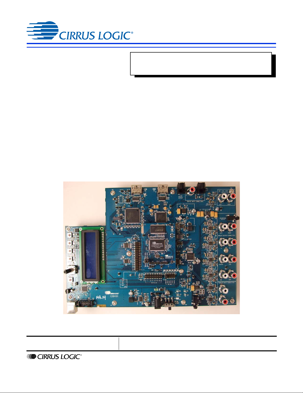
Figure 1-1. CDB49x Evaluation Base Board (without DC4953x Installed) ....................................................1-2
Figure 1-2. CK49x Evaluation System (CDB49x Evaluation Base Board (with DC4953x Installed) .............1-2
Figure 1-3. CDB49x Main Board Block Diagram ...........................................................................................1-4
Figure 1-4. DC4953x Daughter Card Block Diagram ....................................................................................1-4
Figure 1-5. CS495xxx/CS497xxx ADC Clocking.........................................................................................1-11
Figure 1-6. CS495xxx/CS497xxx S/PDIF Clocking .....................................................................................1-12
Figure 1-7. HDMI Clocking ..........................................................................................................................1-13
Figure 2-1. CK49x Evaluation System Block Diagram Using PC Control .....................................................2-1
Figure 2-2. CK49x System Block Diagram in Standalone Mode ...................................................................2-1
Figure 2-3. CDB49x Main Board Top View ...................................................................................................2-3
Figure 2-4. Top View DC4953x/DC4953x3/DC4970x4 Daughter Card ........................................................2-5
Figure 3-1. Board Setup and Connection Diagram .......................................................................................3-3
Figure 3-2. Cirrus Device Manager Icon ......................................................................................................3-4
Figure 3-3. Cirrus Device Manager as Displayed after Double-clicking the CDM Icon .................................3-4
Figure 3-4. Opening a Console Window from Cirrus Device Manager .........................................................3-5
Figure 3-5. CDM Device Console Window ....................................................................................................3-5
Figure 3-6. PCM Pass-through Example Application ....................................................................................3-6
Figure 4-1. System Properties Showing CS495304 as the Chip ID ..............................................................4-1
Figure 4-2. System Properties Showing CS495314 as the Chip ID ..............................................................4-2
Figure 4-3. CK49x DAO Channel Remap .....................................................................................................4-2
Figure 4-4. CK49x Audio In Properties..........................................................................................................4-3
Figure 4-5. CK49x S/PDIF Rx Properties ......................................................................................................4-3
Figure 4-6. CK49x Analog Properties............................................................................................................4-4
Figure 4-7. DSP Composer Support for HDMI Audio Input via I2S ...............................................................4-5
Figure 4-8. CK49x DAI Input Properties ........................................................................................................4-6
Figure 4-9. CK49x Audio Out Properties .......................................................................................................4-7
Figure 4-10. CK49x Digital Audio Output Properties .....................................................................................4-7
Figure 4-11. CK49x Comm Mode / Memory Usage ......................................................................................4-8
Figure 5-1. Close-up View of the CK49x Evaluation System Push Buttons and Rotary Knob ......................5-3
Figure 5-2. LED Status Display: Current Audio Stream Sample Rate ..........................................................5-5
Figure 5-3. Using the Rotary Know to Increments/Decrements the Volume .................................................5-6
Figure 5-4. Setting the Audio Source ............................................................................................................5-6
Figure 5-5. Setting Surround Mode ...............................................................................................................5-7
Figure 5-6. Setting the Virtualizer Mode........................................................................................................5-7
Figure 5-7. Setting the Bass Management Mode..........................................................................................5-8
Figure A-1. DC1: DAI Record and Asio Play Block Diagram ....................................................................... A-2
Figure A-2. DC1: DAI Record and Asio Play ................................................................................................ A-3
DS898CK7 Copyright 2012 Cirrus Logic, Inc
Page 7

CK49x User’s Manual
Table 1-1. CK49x Customer Kit Contents .....................................................................................................1-1
Table 1-2. ADC Clocking.............................................................................................................................1-11
Table 1-3. S/PDIF Clocking .........................................................................................................................1-12
Table 1-4. HDMI Clocking ...........................................................................................................................1-13
Table 2-1. HDMI Clocking .............................................................................................................................2-6
Table 5-1. Options for when S5 Button/Rotary Knob is Turned ....................................................................5-3
DS898CK7 Copyright 2012 Cirrus Logic, Inc
Page 8
CK49x Customer Kit Contents
CK49x User’s Manual
Chapter 1
Customer Kit Contents and Requirements
1.1 CK49x Customer Kit Contents
Table 1-1. CK49x Customer Kit Contents
Customer Kit Item Quantity
CK49x-49530
CK49x-49531
CK49x-495303
CK49x-4953131
CK49x-497024
CK49x-497014
CK49x-49530
CK49x-49531
CK49x-495303
CK49x-4953131
CK49x-497024 DC497024 Daughter Card (128-pin package) with CS497024 DSP 1
CK49x-497014
CK49x-49530
CK49x-49531
CK49x-495303
CK49x-4953131
CK49x-497024
CK49x-497014
CK49x-49530
CK49x-49531
CK49x-495303
CK49x-4953131
CK49x-497024
CK49x-497014
CK49x-49530
CK49x-49531
CK49x-495303
CK49x-495313
CK49x-497024
CK49x-497014
1
1
CDB49x Evaluation Board
4
1
1
DC49530 Daughter Card (128-pin package) with CS495304 DSP 1
3
DC49531
Daughter Card (128-pin package) with CS495314 DSP
DC49503 Daughter Card (128-pin package) with CS495303 DSP 1
2
1
1
DC49513 Daughter Card (128-pin package) with CS495313 DSP 1
4
1
DC497014 Daughter Card (128-pin package) with CS497014 DSP 1
Power Supply: +9V, 2A, 100V - 240V with AC Power Cord 1
4
1
USB Cable (USB 2.0) 1
4
1
1
4
Document Card explaining how to get the latest board software 1
1. Not available for ordering.
2. In this manual, the main (large) board is called the “CDB49x Evaluation Board as shown in Figure 1-1.” When
a daughter card is installed on the CDB49x Evaluation Board as shown in Figure 1-2, the board is then called
the “CK49x Evaluation System”
3. DC49531 is being renamed to DC495314.
4. Use the DC497014 daughter card when implementing firmware other than firmware from DTS.
DS898CK7 Copyright 2012 Cirrus Logic, Inc 1-1
Page 9
Requirements
DC4953x Daughter Card
CK49x User’s Manual
.
Figure 1-1. CDB49x Evaluation Base Board (without DC4953x Installed)
1.2 Requirements
1.2.1 PC Requirements
1.2.2 Software Requirements
1.2.3 Support Hardware Requirements
DS898CK7 Copyright 2012 Cirrus Logic, Inc 1-2
•Microsoft® Windows XP® Operating System
• USB 2.0 Support
• Cirrus Board Software Package (available from your local Cirrus Logic representative)
• Digital or Analog Audio Source (for example, DVD player, PC with a digital audio card/device)
• Amplified Speakers for audio playback (for example, powered PC speakers, AVR/amp + speakers)
Figure 1-2. CK49x Evaluation System (CDB49x Evaluation Base Board (with DC4953x Installed)
Page 10

Requirements
CK49x User’s Manual
1.2.4 Cabling Requirements
• Digital Audio Inputs – HDMI cables, S/PDIF optical cables, RCA audio cables (Connect to digital
audio card, audio analyzer, or DVD player), 20-pin ribbon cable (Play I
card)
• Digital Audio Output – HDMI cables, S/PDIF Optical cable, RCA audio cable (Connect to digital
audio card, audio analyzer, or AV), 20-pin ribbon cable (Record I
• Analog Audio Inputs – RCA audio cables (Connect CK49x line-level inputs to analog audio source)
• Analog Audio Outputs – RCA audio cables (Connect CK49x line-level outputs to powered speakers
or AVR), 1/8” stereo headphone cable (Connect CK49x line-level output to headphones)
2
S audio from digital audio
2
S audio from digital audio card)
1-3 Copyright 2012 Cirrus Logic, Inc. DS898CK7
Page 11
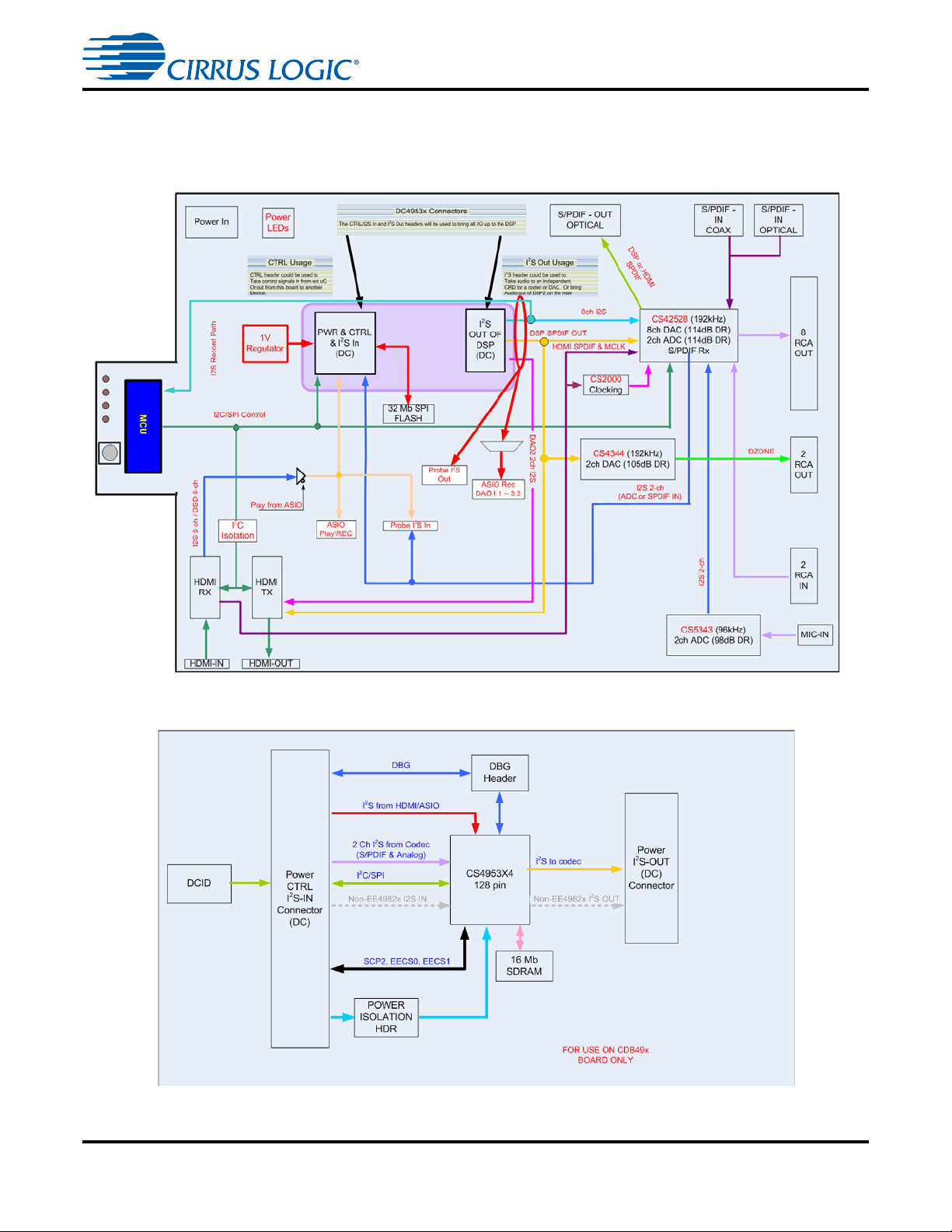
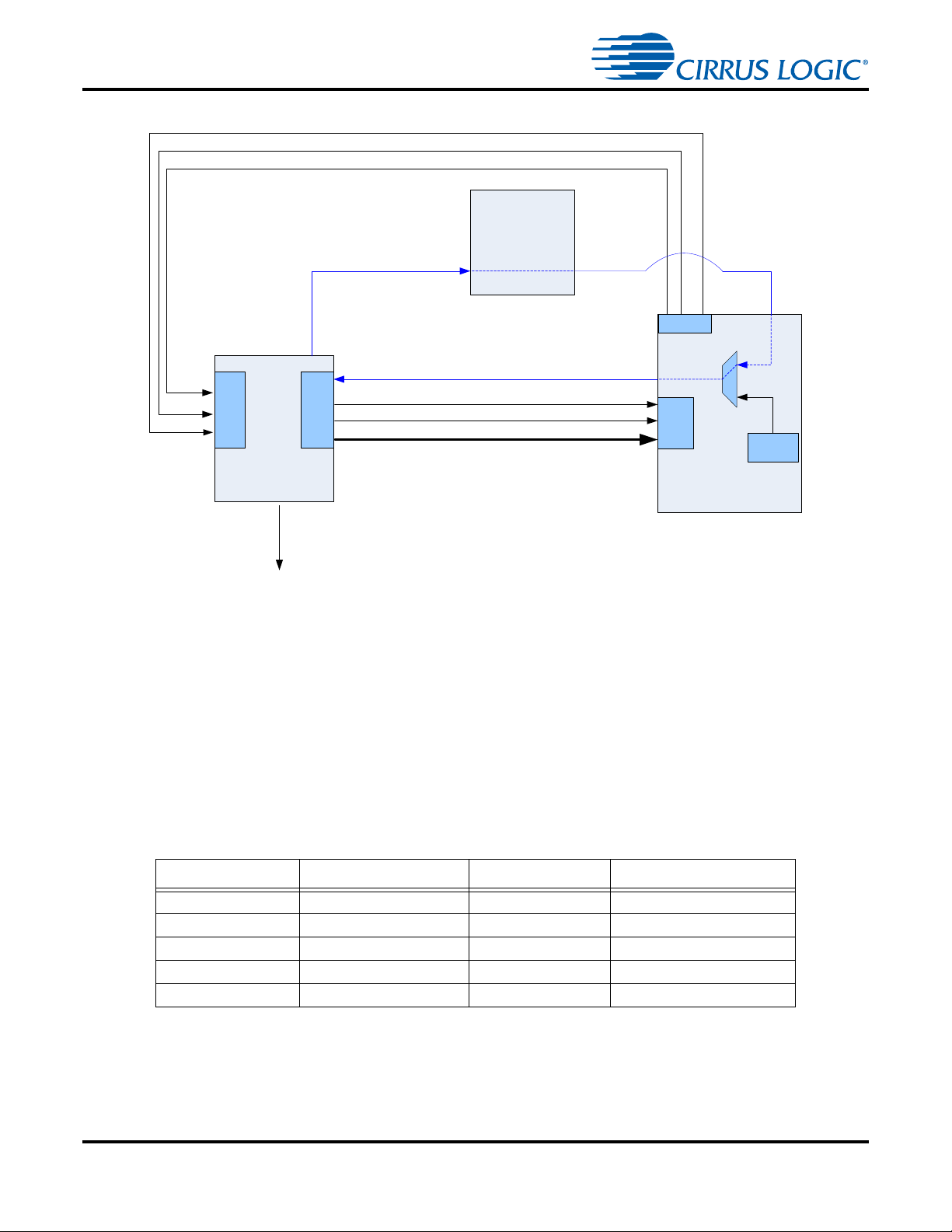
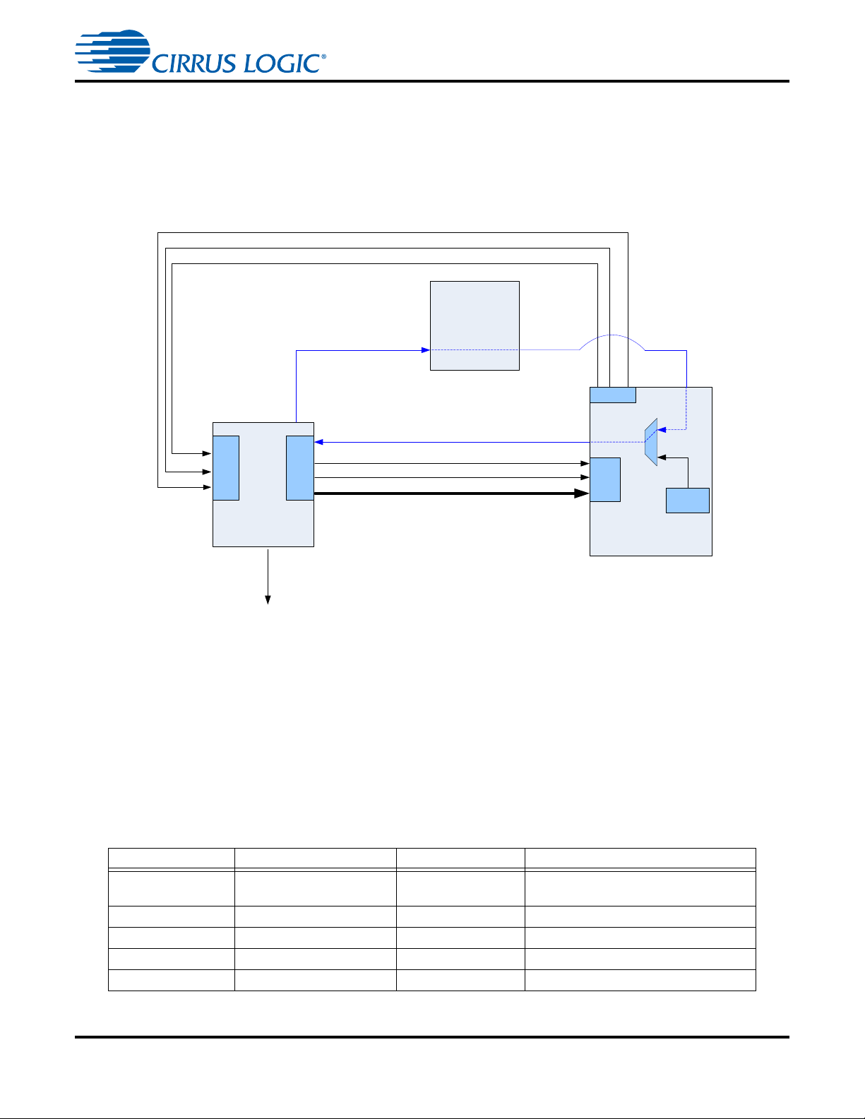
1.3 CK49x System Description
A block diagram of the CDB49x main board is shown in Figure 1-3 and a block diagram of the DC4953x
daughter card in Figure 1-4. The sections that follow provide a detailed description of each block.
CK49x System Description
CK49x User’s Manual
Figure 1-3. CDB49x Main Board Block Diagram
Figure 1-4. DC4953x Daughter Card Block Diagram
DS898CK7 Copyright 2012 Cirrus Logic, Inc 1-4
Page 12

CK49x System Description
CK49x User’s Manual
1.3.1 Audio Inputs
1.3.1.1 Analog Line-level Inputs
Analog line-level inputs have the following characteristics:
• Connector Type: RCA Female
• Absolute Maximum Signal Level: +12Vp-p
• Full Scale Amplitude: 2V
• Reference Designators: J26,J28, or LEFT-IN, RIGHT-IN
1.3.1.2 HDMI Digital Input
HDMI digital inputs have the following characteristics:
• Connector Type: HDMI Type A Female
• Reference Designators: J4, or HDMI RX
1.3.1.3 Optical Digital Inputs
Optical digital inputs have the following characteristics:
RMS
• Connector Type: Fiber Optic RX for Digital Audio, JIS F05 (TOSLINK)
• Reference Designators: J8, or RX0
1.3.1.4 Coaxial Digital Inputs
Coaxial digital inputs have the following characteristics:
• Connector Type: RCA Female
• Maximum Signal Level: 5Vp-p
• Reference Designators: J31, or RX1
1.3.1.5 I2S Digital Input
Coaxial digital inputs have the following characteristics:
• Connector Type: 0.100” Male Header
• Maximum Signal Level: +3.3V
• Reference Designator: P3
1.3.1.6 Microphone Input
The microphone input has the following characteristics:
• Connector Type: 3.5mm (1/8”) Stereo Female
• Absolute Maximum Signal Level: 14.3mVp-p
• Full Scale Amplitude: 6.5mVp-p
• Reference Designator: J5
1-5 Copyright 2012 Cirrus Logic, Inc. DS898CK7
Page 13

1.3.2 Audio Outputs
1.3.2.1 Main Analog Line-level Outputs
Analog line-level outputs have the following characteristics:
• Connector Type: RCA Female
• Full Scale Amplitude: 2V
• Reference Designators: J33-J40, or LEFT, RIGHT, Ls, Rs, CENTER, SUB, SBL, SBR
1.3.2.2 Headphone Output
Analog line-level outputs have the following characteristics:
• Connector Type: 3.5mm (1/8”) Stereo Female
• Full Scale Amplitude: 2V
• Reference Designators: J12, or HEADPHONE OUT
The headphone output shares the same Op Amp that drives Main LEFT/RIGHT outputs, which means
that headphone content will always be the same as Main LEFT/RIGHT. Only one pair of outputs should be
connected to a load - either HEADPHONE OUT or J34/J36.
RMS
RMS
CK49x System Description
CK49x User’s Manual
1.3.2.3 Dual Zone Analog Line-level Outputs
Analog line-level outputs have the following characteristics:
• Connector Type: RCA Female
• Max Full Scale Amplitude: 1.23V
• Reference Designators: J1, J10, or LEFT, RIGHT
1.3.2.4 HDMI Digital Output
HDMI digital outputs have the following characteristics:
• Connector Type: HDMI Type A Female
• Reference Designators: J6, or HDMI TX
1
RMS
1.3.2.5 Optical Digital Output
The optical digital output has the following characteristics:
• Connector Type: Fiber Optic TX for Digital Audio, JIS F05 (TOSLINK)
• Reference Designator: J24, or DIGITAL OUTPUT
1.3.2.6 I2S Digital Output
I2S digital output has the following characteristics:
• Connector Type: 0.100” Male Header
• Maximum Signal Level: +3.3V
• Reference Designator: P12
1. HDMI Digital Output is not currently supported.
DS898CK7 Copyright 2012 Cirrus Logic, Inc 1-6
Page 14

CK49x System Description
CK49x User’s Manual
1.3.2.7 I2S Digital Output (DAO Mux Output)
I2S digital output has the following characteristics:
• Connector Type: 0.100” Male Header
• Maximum Signal Level: +3.3V
• Reference Designator: P16
1.3.3 DC Power Input
The DC power input has the following characteristics and is switched by S7:
• Voltage Range: +9V
• Minimum Power: 18W supply (2A @ 9V)
• Connector Type: 2mm Female, positive center pin
• Reference Designator: J25
DC TO +12VDC
1.3.4 USB Connector
The control header has the following characteristics:
• Connector Type: USB Standard B Connector
• Reference Designator: J2
This connector is the interface between the CK49x and the PC.
1.3.5 MCU Programming Header
This header is used to program the MCU from a Silicon Labs programming dongle. This is not for
customer use, and should be used only by Cirrus FAEs for upgrading the board.
• Connector Type: 0.100” Shrouded Male Header
• Reference Designator: J9
1.3.6 Reset button
The button S6 (located near the USB connector J2) is used to reset the MCU. In stand-alone mode this
will re-initialize the entire board and start the stand-alone program over from the beginning.
In USB-control mode, this button will re-initialize the board and force the device to re-enumerate itself on
the PC USB interface.
1.3.7 Buttons and Knobs
The buttons S1 - S4 (located near the LCD) are used for controlling the MCU when in stand-alone mode.
The knob S5 is also used for controlling the MCU when in stand-alone mode.
1.3.8 DAO MUX Select Header
The DAO outputs of the DSP are sent to a mux that drives I2S Digital Output header P16. The signals
driven to P16 are selected by the Header P17. Only 1 shunt may be installed on header P17 at any time.
Using more than 1 shunt will cause multiple buffers to drive their outputs simultaneously and cause
contention.
1-7 Copyright 2012 Cirrus Logic, Inc. DS898CK7
Page 15

The output buffer currently enabled is indicated by the LEDs D18 - D23.
1.3.9 DAI1 Audio Input Source Multiplexer
The audio input source multiplexer has the following characteristics:
• Source 0 [shunt removed]: HDMI RX I2S Audio
• Source 1 [shunt installed]: I
2
S Audio (ASIO I2S Board)
• Reference Designators: U15, U28
This multiplexer is controlled by pins 1-2 of header P4, and is used to select which audio source feeds the
CS495xxx/CS497xxx DAI1 pins when the ASIO I
2
S Board is installed. When the on-board sources (HDMI
RX) are being used, the ASIO audio data cannot be processed. Likewise, when the ASIO audio data
2
source (ASIO I
S Board) is selected, the on-board audio inputs are disabled.
1.3.10 DAI2 Audio Input Source Multiplexer
The audio input source multiplexer has the following characteristics:
• Source 0: CS42528 Audio (ADC or S/PDIF)
• Source 1: Bi-Phase Encoded S/PDIF Signal
• Reference Designator: U23
CK49x System Description
CK49x User’s Manual
This multiplexer is controlled by GPO1 of the CS42528 (U5), and is used to select which audio sources
feed the CS495xxx/CS497xxx DAI2 pins. When the DSD audio from HDMI RX is being used, the
CS42528 data cannot be processed. Likewise, when the CS42528 audio is selected, the HDMI RX DSD
audio is disabled.
1.3.11 CS495xxx/CS497xxx Audio DSP
The audio DSP (U1 on DSP Daughtercard) is a dual-core processor designed specifically for audio
applications. The CK49x allows a designer to evaluate the CS495xxx/CS497xxx DSPs in many different
modes of multi-channel input and output. The 128-pin footprint on this board is compatible with any
CS495xxx/CS497xxx chip that uses the LQFP128 package.
Audio input data to the DSP can come from any of the following sources:
• CS42528 Line-Level Analog In
• CS42528 Microphone Analog In
• CS42528 Digital S/PDIF In
• HDMI RX
2
•I
S Through ASIO I2S Board (feature not currently supported)
Audio output data from the DSP can be sent to the following destinations:
• CS42528 Line-Level Analog Output
• CS42528 Headphone Analog Output
• CS42528 Digital S/PDIF Out
• HDMI TX
2
•I
S Through Header P16
DS898CK7 Copyright 2012 Cirrus Logic, Inc 1-8
Page 16

CK49x System Description
CK49x User’s Manual
The CS4953xx/CS4970x4 has many applications stored in internal ROM, but a host is still required to
configure the application for a particular system. The CK49x allows the PC to act as a host to boot and
configure the DSP through the GUI software.
The DSP is booted primarily from external serial Flash (U13 on CDB49x) using the DSP Condenser
system for simplified MCU control.
1.3.12 Debug Header
The DC49xxx daughtercard (DSP daughtercard) has a debug port (TP13) intended for factory testing of
the DSP. By default, shunts are installed across the header to allow debug from the attached MCU. If the
jumpers are removed, it is possible to debug the DSP using an external controller.
1.3.13 CS2000 Clock Synthesizer
The CS2000 (U25) is a high performance clocking device that is used to reduce jitter on recovered clocks
through the use of a low-jitter PLL and clean reference clock. The CS2000 is used on this board to reduce
the jitter on the MCLK recovered from an HDMI link.
The CS2000 can also be programmed to pass the reference clock (XTAL_OUT from the DSP) directly to
the CS42528 audio CODEC and S/PDIF RX.
1.3.14 CS42528 S/PDIF RX
The CS42528 (U5) has an integrated 192 kHz S/PDIF receiver with an input multiplexer. All of the S/PDIF
sources on the board (RX0, RX1, DSP, U16) are connected to the CS42528 input multiplexer. The active
S/PDIF signal is selected by changing the internal mux through the serial host port of the CS42528. This
selection is controlled through the Audio In configuration within DSP Composer (see
"Programming the DSP on the CK49x Evaluation Board"
When S/PDIF audio is being processed, the CS42528 must master MCLK for the system (see Figure 1-6
for details).
1.3.15 CS42528 Audio CODEC
The CS42528 (U5) is a high-performance, multi-channel audio CODEC capable of supporting sample
rates up to 192 kHz on its 2 ADCs and 8 DACs. This device is used for main-channel analog-to-digital and
digital-to-analog conversions on the CK49x.
All analog inputs (J5, J26, J28) and 8 of the analog outputs (J33 - J40) are connected to the CS42528.
The microphone input (J5) uses an external ADC (U7) to feed the dedicated ADC input of the CS42528.
When the microphone is in use, a special TDM format is used to deliver the digitized microphone audio to
the DSP via the SAI data output of the CS42528.
When analog audio is being processed, the 24.576 MHz crystal for the CS495xxx/CS497xxx must master
MCLK for the system (see ‘Audio Clocking on page 1-10 for details).
Chapter 4,
for details).
1.3.16 CS4344 DAC
The CS4344 (U3) is a high-performance, 2-channel DAC capable of converting audio data with sample
rates up to 192 kHz. This device is used for the dual-zone digital-to-analog conversions on the CK49x.
Analog outputs (J1, J10) are connected to the CS4344. The dual-zone DAC is connected to the DAO2
port of the CS495xxx/CS497xxx to allow up to 10 channels of simultaneous analog output.
1-9 Copyright 2012 Cirrus Logic, Inc. DS898CK7
Page 17

1.3.17 HDMI Recevier (RX)
The Silicon Image™ Si9135 HDMI Rx (U16) is used for the HDMI input on the CK49x. It can provide up to
2
4 lines of I
streams.
Because the Si9135 responds to all I
HDMI Rx from responding to serial communication intended for other devices on the CK49x.
S data which can support PCM, legacy compressed audio (DD, DTS), and new HD audio
1.3.18 HDMI Transmitter (TX)
The Silicon Image Si9134 HDMI Tx (U19) is used for the HDMI output on the CK49x.
Note: The HDMI Tx function is currently not supported on the CK49x.
Because the Si9134 responds to all I
HDMI Tx from responding to serial communication intended for other devices on the CK49x.
1.3.19 Memory
The CDB49x is assembled with a 32-Mbit serial Flash (U13).
CK49x System Description
CK49x User’s Manual
2
C addresses, a bus isolator (U14) has been used to prevent the
2
C addresses, a bus isolator (U14) has been used to prevent the
The CS495xxx/CS497xxx can use external SDRAM (U15 on DC4953x) to implement features such as
large multi-channel audio delays. A 16 Mbit SDRAM (200 MHz) is connected to the 150 MHz memory bus
of the CS495xxx/CS497xxx.
1.3.20 Audio Clocking
Clocking architecture is one of the most important aspects of an audio system. The input and output clock
domains of the DSP must be synchronous when delivering audio data in an isochronous fashion (constant
bit-rate delivery), even if the input/output domains operate at different frequencies (e.g. 48 kHz input/96
kHz output). Systems utilizing I
isochronous delivery.
The requirements are slightly more complicated for systems using “bursty” delivery on the input side of the
DSP, but the CK49x is designed to emulate isochronous systems.
The CK49x can operate in three different clocking modes. Each of these modes is explained in the
following sections.
2
S delivery of S/PDIF input, ADC input, or other digital audio input use
DS898CK7 Copyright 2012 Cirrus Logic, Inc 1-10
Page 18
CK49x System Description
OUT_DAO1_SCLK
OUT_DAO1_LRCLK
OUT_DA01_D[3:0]
XMTA S/PDIF
OUT
MUXED_BUF_MCLK
DAI DAO
SDIN
CS42528
XTAL_OUT
CS2000
S/PDIF
RX
CODEC_SCLK
CODEC_LRCLK
CODEC_DOUT
SDOUT
CS4953x
DSP-1
CK49x User’s Manual
1.3.20.1 Clock and Data Flow for ADC Input
Figure 1-5. CS495xxx/CS497xxx ADC Clocking
The ADC clocking architecture is used when the ADCs are used as the only audio input (i.e. S/PDIF is
disabled, and the audio input source multiplexer (U23) is used to select CODEC audio sources. Figure 1-
5 illustrates this clocking configuration.
XTAL_OUT from the CS495xxx/CS497xxx is MCLK for the system via the CS2000 and CS42528 clocking
mux, and the codec masters the input clocks (MUXED_SCLK/MUXED_LRCLK) of the CS495xxx/
CS497xxx. The system routing of the clocks was simplified by using the CS42528 to drive MCLK to the
system, but the internal clock multiplexer of the CS42528 is forced to the OMCK setting to pass
XTAL_OUT.
The CS495xxx/CS497xxx always masters its output clocks (OUT_DAO1_SCLK/OUT_DAO1_LRCLK).
MUXED_BUF_MCLK CS495xxx/CS497xxx CS42528 24.576 MHz
OUT_DAO1_LRCLK MUXED_BUF_MCLK CS495xxx/CS497xxx 1*Input Fs (default)
CODEC_LRCLK MUXED_BUF_MCLK CS42528 Input Fs
OUT_DAO1_SCLK MUXED_BUF_MCLK CS495xxx/CS497xxx 64*Output Fs (default)
Table 1-2. ADC Clocking
Clock Name Clock Master Source Clock Driver Clock Frequency
CODEC_SCLK MUXED_BUF_MCLK CS42528 64*Input Fs (default)
1-11 Copyright 2012 Cirrus Logic, Inc. DS898CK7
Page 19
Note: MUXED_MCLK is the clock signal that is driven by the CS42528’s RMCK pin. The CS42528
OUT_DAO1_SCLK
OUT_DAO1_LRCLK
OUT_DA01_D[3:0]
XMTA S/PDIF
OUT
MUXED_BUF_MCLK
DAI DAO
SDIN
CS42528
XTAL_OUT
CS2000
S/PDIF
RX
CODEC_SCLK
CODEC_LRCLK
CODEC_DOUT
SDOUT
CS4953x
DSP-1
provides the recovered clock from the S/PDIF input unless it loses signal lock, in which case the
CS42528 passes the DSP clock (XTAL_OUT) that it receives on the OMCK pin via the CS2000.
1.3.20.2 Clock and Data Flow for S/PDIF Input
CK49x System Description
CK49x User’s Manual
Figure 1-6. CS495xxx/CS497xxx S/PDIF Clocking
The S/PDIF clocking architecture is used when any S/PDIF RX is used as an audio source. That is, any S/
PDIF RX is selected, and the audio input source multiplexer (U23) is used to select CODEC audio
sources. Figure 1-6 illustrates this clocking configuration.
MCLK recovered from the incoming S/PDIF stream must be MCLK for the system, and the codec masters
the input clocks (CODEC_SCLK/CODEC_LRCLK) of the CS495xxx/CS497xxx. In this configuration the
internal multiplexer of the CS42528 routes the recovered MCLK to MUXED_MCLK.
The CS495xxx/CS497xxx always masters its output clocks (OUT_DAO1_SCLK/OUT_DAO1_LRCLK).
Clock Name Clock Master Source Clock Driver Clock Frequency
MUXED_MCLK CS42528 CS42528
CODEC_SCLK MUXED_MCLK CS42528 64*Input Fs (default)
CODEC_LRCLK MUXED_MCLK CS42528 Input Fs
OUT_DAO1_SCLK MUXED_MCLK CS495xxx/CS497xxx 64*Output Fs (default)
OUT_DAO1_LRCLK MUXED_MCLK CS495xxx/CS497xxx 1*Input Fs (default)
Note: MUXED_MCLK is the clock signal that is driven by the CS42528’s RMCK pin. The CS42528
Table 1-3. S/PDIF Clocking
512*S/PDIF Fs
(e.g. 24.576 MHz for 48 kHz),
DS898CK7 Copyright 2012 Cirrus Logic, Inc 1-12
Page 20

CK49x System Description
CS4953x4
HDMI RX /
ASIO Input
DAI1_SCLK
OUT_DAO1_SCLK
OUT_DAO1_LRCLK
DAI1_LRCLK
MUXED_DAI[4:0]
DSP_DA0[3:0]
XMTA S/PDIF
OUT
MUXED_BUF_MCLK
DAI DAO
SDIN
CS42528
XTAL_OUT
CS2000
S/PDIF
RX
CK49x User’s Manual
provides the recovered clock from the S/PDIF input unless it loses signal lock, in which case the
CS42528 passes the DSP clock (XTAL_OUT) that it receives on the OMCK pin.
1.3.20.3 Clock and Data Flow for HDMI or ASIO Input Data Delivery
Figure 1-7. HDMI Clocking
When the HDMI or ASIO source is selected, that device masters the system MCLK, and the input clocks
(MUXED_SCLK/MUXED_LRCLK) of the CS495xxx/CS497xxx.
The CS495xxx/CS497xxx always masters its output clocks (OUT_DAO1_SCLK/OUT_DAO1_LRCLK).
Table 1-4. HDMI Clocking
Clock Name Clock Master Source Clock Driver Clock Frequency
MUXED_MCLK HDMI/ASIO Source HDMI/ASIO Source
256*S/PDIF Fs
(e.g. 12.288 MHz for 48 kHz)
DAI1_SCLK MUXED_MCLK HDMI/ASIO Source 64*Input Fs (default)
DAI1_LRCLK MUXED_MCLK HDMI/ASIO Source Input Fs
OUT_DAO1_SCLK MUXED_MCLK CS495xxx/CS497xxx 64*Output Fs (default)
OUT_DAO1_LRCLK MUXED_MCLK CS495xxx/CS497xxx 1*Input Fs (default)
Note: MUXED_MCLK is the clock signal that is driven by the HDMI source.
1-13 Copyright 2012 Cirrus Logic, Inc. DS898CK7
Page 21

1.4 DS898CK4Other Useful Information
1.4.1 Web Sites
• Cirrus Logic main web site: www.cirrus.com
1.4.2 DSP Information
The following information can be obtained from your Cirrus Logic representative.
• CS495xxx/CS497xxx Data Sheet
• CS495xxx/CS497xxx System Designer’s Guide
•AN288, CS495xxx/CS497xxx Firmware User’s Manual
1.4.3 Board Information
• The following information can be obtained from your local Cirrus Logic representative.
• Schematics
•BOM
• Artwork and PCB stack up
DS898CK4Other Useful Information
CK49x User’s Manual
1.4.4 Audio CODEC Information
The following information can be obtained from your local Cirrus Logic representative.
• CS42528 Data Sheet
• CS42528 Errata
1.4.5 DSP Software Utility Information
The following information can be obtained from your local Cirrus representative.
• DSP Composer
• DSP Composer
The documents listed above are updated periodically and may be more up-to-date than the information in
this document. Check the Cirrus Logic web site for the latest updates.
User’s Manual
Primitive Elements Reference
DS898CK7 Copyright 2012 Cirrus Logic, Inc 1-14
Page 22

Introducing the CK49x Evaluation System
HDMI
USB Port
Analog Audio
PC
S/PDIF
Multi-channel I2S
CDB49x
DC4953x
Digital Audio
Card
LCD
HDMI
User Input
Analog Audio
S/PDIF
Multi-channel I2S
CDB49x
DC4953x
Digital Audio
Card
LCD
CK49x User’s Manual
Introduction to CK49x Evaluation System
2.1 Introducing the CK49x Evaluation System
The CK49x Evaluation System is composed of the CDB49x base board and the DC4953x daughter card
where the C24953x4 DSP is installed. The CK49x Evaluation System provides a practical platform for
emulating a typical multi-channel audio system application. The on-board MCU provides a USB control
port used to interface the host PC to the CK49x Evaluation System, and convert GUI commands into the
serial control protocol required for configuring the CS4953x4 DSP, CS42528 and CS2000 audio ICs, and
the HDMI interface chips. Figure 2-1 shows the CK49x Evaluation System when controlled by the user’s
PC. Figure 2-2 shows the CK49x Evaluation System operating in Standalone mode. Standalone mode is
described in detail in Chapter 5.
Chapter 2
2-1 Copyright 2012 Cirrus Logic, Inc. DS898CK7
Figure 2-1. CK49x Evaluation System Block Diagram Using PC Control
Figure 2-2. CK49x System Block Diagram in Standalone Mode
Page 23

Identifying Components on the CK49x Evaluation System
CK49x User’s Manual
This document will concentrate on the features and basic operation of the CK49x board. Detailed
information regarding the operation and programming of the CS4953x4 DSP is covered by the CS4953xx
Data Sheet, the CS4970x4/CS4953x4 System Designer’s Guide and the application note AN288. See
Section 1.4 “DS898CK4Other Useful Information” on page 1-14 for more details.
The CK49x is a convenient and easy-to-operate evaluation platform. It has been designed to demonstrate
the majority of the DSP functions on a 9" x 6.5" base board. These features include:
™
• PC control of the DSP using the DSP Composer
• Serial control of audio devices on CK49x Evaluation System via I
• Digital audio input of PCM or compressed data via optical or coaxial S/PDIF
• Digital audio input of PCM or compressed data via HDMI
• 2-channel analog audio input via the CS42528 audio codec
• 8-channel analog output through the CS42528 audio codec
• Digital audio output of PCM data via optical S/PDIF
• Digital audio output of PCM or compressed data via HDMI (feature not currently supported)
• Multi-channel digital audio input via P11 header (feature not currently supported)
• Separate input and output clocking domains to allow 1FS-to-2FS audio processing on the DSP
• DSP Memory expansion through external 16-Mbit SDRAM
• Fast boot –master boot of custom applications from 32 Mbit serial SPI Flash device.
• Microphone input with integrated amplifier for Intelligent Room Calibration (IRC) evaluation
• Supports all members of the CS495xxx/CS4970x4 family in the 128-pin LQFP package.
graphical user interface
2
C™ or SPI™ protocols
Note: Not all features of the DSP are exercised on the CK49x. Evaluation System
2.2 Identifying Components on the CK49x Evaluation System
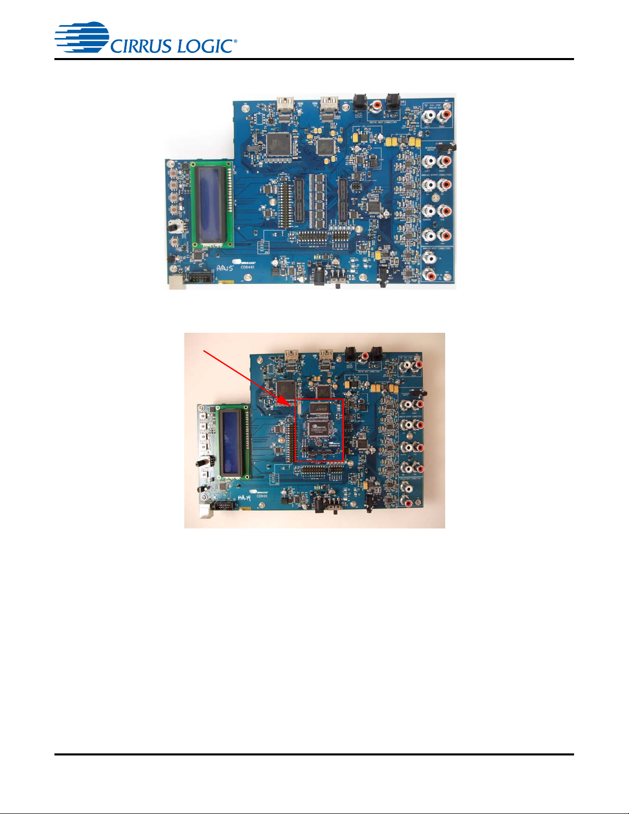
2.2.1 CDB49x Main Board Components
Figure 2-3 shows the top side of the CDB49x Main Board. The accompanying legend identifies the main
components of the board. Section 2.2.1.1 contains the legend for the reference points called out in red in
Figure 2-3.
DS898CK7 Copyright 2012 Cirrus Logic, Inc 2-2
Page 24

DS898CK7 Copyright 2012 Cirrus Logic, Inc 2-3
1
2
3
4
5
6
7
8
9
10
11
12
13
14
15
16
17
18
19
24
21
20
22
23
27
25
28
29
26
30
31
33
34
36
35
38
37
32
Identifying Components on the CK49x Evaluation System
Figure 2-3. CDB49x Main Board Top View
CK49x User’s Manual
Page 25

2.2.1.1 CDB49x Main Board Components
The circled numbers found in Figure 2-3 refer to the CDB49x Main Board components in the following list:
1. LCD
2. HDMI Receiver (Rx)
3. Extended Display Identification Data (EDID) Programming Header
4. HDMI Input Connector
5. Hot Plug Indicator
6. HDMI Transmitter (Tx)
7. HDMI Output Connector
8. S/PDIF Optical Tx
9. S/PDIF Coax Rx
10. S/PDIF Optical Rx
11. +5V Header
12. +1.8V Header
Identifying Components on the CK49x Evaluation System
CK49x User’s Manual
13. Dual Zone Analog Outputs
14. Headphone Output
15. Main Analog Line-Level Outputs (Left/Right; Left Surround/Right Surround; Center/Subwoofer;
Surround Back Left/Surround Back Right)
16. Cirrus Logic CS42528 CODEC
17. Cirrus Logic CS2000 Clock Generator and Clock Multiplier/Jitter-Reduced Clock Frequency
Synthesizer
18. DAO Selection
19. Analog Line-Level Input
20. Mic Input
21. Power Indicator LEDs (4)
22. Slave Boot Control
23. Power Switch
24. +9V Power Connector
25. DAO Mux Header
26. +3.3V Header
27. Daughter Card Connectors (2)
28. DAI 1, 2, and 3 Header
29. DSD/I
2
S Mux LED
30. MCU Programming Header (C2 Header)
31. USB Connector
32. USB Active LED
33. 8051 MCU
DS898CK7 Copyright 2012 Cirrus Logic, Inc 2-4
Page 26

Identifying Components on the CK49x Evaluation System
1
2
3
4
5
CK49x User’s Manual
34. IR Receiver
35. System Reset
36. Rotary Encoder Knob
37. MCU Buttons (4) (Menu, Left, Right, Exit)
38. MCU LEDs (4)
2.2.2 DC4953x Daughter Card
Figure 2-4 shows the top side of the DC4953x Daughter Card. The accompanying legend identifies the
main components of the board. Section 2.2.2.1 contains the legend for the reference points called out in
red in Figure 2-4.
Figure 2-4. Top View DC4953x/DC4953x3/DC4970x4 Daughter Card
2-5 Copyright 2012 Cirrus Logic, Inc. DS898CK7
Page 27

Identifying Components on the CK49x Evaluation System
2.2.2.1 DC4953x Daughter Card Components
The circled numbers found in Figure 2-4 refer to the DC4953x Daughter Card components in the following
list:
1. Cirrus Logic CS4953x DSP (U1)
2. 24.576 MHz Crystal (Y1)
3. Debug Header (P5)
4. ESMT 16-Mbit SDRAM (U2)
5. Power LEDs (2)
2.2.2.2 DC4970x4 Daughter Card Components
The circled numbers found in Figure 2-4 refer to the DC4970x4 Daughter Card components in the following
list:
1. Cirrus Logic CS4970x4 DSP (U1)
2. 24.576 MHz Crystal (Y1)DS898CK4
3. Debug Header (P5)
CK49x User’s Manual
4. ESMT 16-Mbit SDRAM (U2)
5. Power LEDs (2)
2.2.2.3 DC4953x3 Daughter Card Components
The circled numbers found in Figure 2-4 refer to the DC4953x3 Daughter Card components in the following
list:
1. Cirrus Logic CS4953x3 DSP (U1)
2. 24.576 MHz Crystal (Y1)
3. Debug Header (P5)
4. ESMT 16-Mbit SDRAM (U2)
5. Power LEDs (2)
Table 2-1. HDMI Clocking
Daughter Card
Var iants
DC495303 R89,R87,R81 R90,R85,R86
DC495313 R90,R85,R86 R89,R87,R81
DC495304 R89,R85,R81 R90,R87,R86
DC495314 R89,R87,R86 R90,R85,R81
DC497024 R85,R89,R86 R90,R87,R81
Populate Do Not Populate
DS898CK7 Copyright 2012 Cirrus Logic, Inc 2-6
Page 28

Installation, Setup, and Running First Application
CK49x User’s Manual
Installation, Setup, and Running Application
3.1 Installation, Setup, and Running First Application
It is important to install the Board Software BEFORE connecting the USB cable. Failure
to install the board software before the initial connection can result in an inability to
communicate with the CDB49x.
3.1.1 Board Software Installation
The DSP board software installation will first install the Cirrus Logic DSP board software followed by the
installation of the required USB drivers.
1. Run the latest DSP board software installation executable (CS4953x_eval_kit_rc**.exe or later). This
executable is supplied by your Cirrus Logic representative.
Chapter 3
2. At the Welcome screen, click Next.
3. At the Licensing Agreement window, select the “I accept the agreement” radio button to agree to the
terms and then select Next.
4. Select the Destination Location window, Select the default location “C:\CirrusDSP” and click Next.
5. Select Start Menu Folder window, Select the default location “C:\CirrusDSP” and click Next.
6. The Ready to Install window indicates the selected destination location and the Start menu folder for
confirmation, select Install to begin the install process which should take less than one minute. When
the software is being installed, release notes of the various components are opened. Release notes
are stored in C:\CirrusDSP\cs49xxx\doc\release_notes for future reference.
7. The Cirrus DSP board software will then prompt the user to click Finish to exit the setup wizard.
3.1.2 Setting up the CK49x Evaluation Board
Follow these steps to set up the CK49x Evaluation Board
1. Place the CDB49x on a static-free surface
2. Plug in the DSP daughter Card to the CDB49x base board. This board is now called the CK49x
Evaluation System.
3. Connect the power supply jack to the CK49x Evaluation System as shown in Figure 3-1 and the
adapter to a wall power socket or power strip.
4. Verify that 4 MCU LEDs on the CDB49x base board and the 2 LEDs on the daughter card are
illuminated.
5. The LCD Display on the Screen is Blank.
6. Connect a SPDIF source the CK49x Evaluation System
• Connect one end of the digital audio S/PDIF optical RX cable on the CK49x Evaluation System
3-1 Copyright 2012 Cirrus Logic, Inc. DS898CK7
Page 29

Installation, Setup, and Running First Application
CK49x User’s Manual
• Connect the other end of the optical cable to the optical output on the back of a DVD player or other
digital audio source.
7. Connect powered speaker to the CK49x Evaluation System:
• Use the RCA audio cables to connect the line-level analog outputs to powered speakers as shown in
Figure 3-1.
DS898CK7 Copyright 2012 Cirrus Logic, Inc 3-2
Page 30

DS898CK7 Copyright 2012 Cirrus Logic, Inc 3-3
USB
Cable
DVD Player
S/PDIF Optical Rx Cable
RCA Cables to
Powered Speakers
RCA Cables to
Powered Speakers
Power
Cable
S/PDIF Optical Tx
Analog
Outputs
USB
2.0 Port
“A”
“B”
Analog Line Level Inputs
+9V
Power
Supply
L
Dual Zone Outputs
R
Ls
Rs
Center
Sub
SBL
SBR
MCU Push Buttons
MCU Rotary Knob
MCU LEDs (4)
HDMI In
For Video
Installation, Setup, and Running First Application
CK49x User’s Manual
Figure 3-1. Board Setup and Connection Diagram
Page 31

3.1.3 Connecting to a PC
Note: There is a possibility that the CK49x Evaluation Board may disconnect from the PC during
operation. It is recommended to short across pads of R97 and C203 by the USB connector on
the board to avoid any USB connectivity issues.
Follow these steps, to connect the PC
1. Connect the “B” end of the USB cable to P1 on the CK49x Evaluation System.
2. Connect the “A” end of the USB Cable to a USB 2.0 port on a notebook or PC running Windows XP
3. The LCD displays “Wait for USB enumeration…” message first and then shows the board name,”
CK49x”, “USB” which signifies that a USB connection is active, and the MCU firmware revision
number that is currently active.
4. On the PC the “Found new Hardware” message will be displayed and the necessary USB device
drivers will be installed automatically
5. In the system tray an icon called CDM (Cirrus Device Manager) will be running as shown in
Figure 3-2.
Caution: The Cirrus Device Manager must be running in order for the board to operate correctly.
Installation, Setup, and Running First Application
CK49x User’s Manual
.
6. The CDM icon stays gray in color until the board is detected. Once the board is detected the icon
turns dark blue as shown in Figure 3-2.
Figure 3-2. Cirrus Device Manager Icon
7. Double click on the icon to open up CDM and verify that the board listed is correct. An example with
DC49531 is shown in Figure 3-3.
Figure 3-3. Cirrus Device Manager as Displayed after Double-clicking the CDM Icon
3.1.4 Opening a Console Window from the Cirrus Device Manager
1. Double click on the system tray icon to open up CDM
2. Right click on the board that is listed/detected (e.g.: CS495314_board), and click on “Start Console”
menu option, as shown in Figure 3-4.
DS898CK7 Copyright 2012 Cirrus Logic, Inc 3-4
Page 32

Installation, Setup, and Running First Application
CK49x User’s Manual
Figure 3-4. Opening a Console Window from Cirrus Device Manager
3. Figure 3-5 shows the CDM Console window, which is now available for the user to enter commands.
Figure 3-5. CDM Device Console Window
DS898CK7 Copyright 2012 Cirrus Logic, Inc 3-5
Page 33

Installation, Setup, and Running First Application
CK49x User’s Manual
3.1.5 Running a Stereo PCM Application on CK49x
Figure 3-6 shows the DSP Composer™ main window for a PCM pass-through application on the CK49x.
The blocks shown in the main window of DSP Composer™ can be selected from the folders in the lefthand window pane, and then connected together by “wires” to indicate the processing path as shown
The “Audio In” and “Audio Out” blocks represent the hardware ports that need to be configured. The
“Audio In” block is used to select the S/PDIF Input or Analog or HDMI input that is to be processed, and
configure the digital audio format for the CS42526’s ADC, SiI9135 HDMI Rx, and the CS4953x4 DAI port.
The “Audio Out” block is used to configure the digital audio format for the CS495xxx/CS497xxx DAO port,
the CS4252’s8 DACs, and enable or disable the S/PDIF TX output of the CK49x.
Figure 3-6. PCM Pass-through Example Application
To run a stereo PCM application on the CK49x Evaluation System, follow these steps:
1. Launch DSP Composer
- If DC4953xxx is used, Start
- If DC4970x4 is used, Start
2. In DSP Composer, go to File
C:\CirrusDSP\CS4953X\projects\<pcm_spp_spdif_input_49xxx>.cpa. depending on the DSP
daughter card used on the CK49x evaluation platform.
3. Press the GO button
4. Insert PCM material into the DVD player (e.g. music CD). If a DVD is being used as the audio source,
make sure that the DVD Player (or other digital audio source) is configured to output PCM data and
S/PDIF out of the player connected to RX0 on the board.
5. Press Play on the DVD player (or other digital audio source). You should now hear audio from the
speakers.
Note: Click on File->Properties in DSPComposer and make sure the board connected field is set to
CDB49x
3-6 Copyright 2012 Cirrus Logic, Inc. DS898CK7
Program Cirrus DSP CS495xxx/CS497xxx
Program Cirrus DSP CS497x
Open and open
Page 34

Installation, Setup, and Running First Application
CK49x User’s Manual
3.1.6 Downloading Other Applications
Separate project files (.cpa) are provided for other applications such as Dolby Digital. In order to evaluate
these, please contact your local FAE to ensure that the necessary licensing agreements have been
completed.
3.1.7 Running a Multichannel PCM Application via HDMI
The CK49x Evaluation System includes an HDMI 1.3–compliant receiver (Sil9135; To receive support for
the SiI9134 and SiI9135 chips, contact Silicon Image, Inc.) and an HDMI 1.32–compliant transmitter
(Sil9134), both of which are manufactured by Silicon Image, Inc.
To play multi-channel PCM via HDMI, follow the configuration and connections shown in Figure 3-1.
1. Open the appropriate .cpa file
- For the DC4953x3, use the CS4953x->DSPComposer menu option and open:
C:\CirrusDSP\CS4953x\projects\pcm_mch_spp_hdmi_input_4953x3.cpa.
- For the DC4970x4, use the CS497xx ->DSPComposer menu option and open:
C:\CirrusDSP\CS4953x\projects\pcm_mch_spp_hdmi_input_4970x4.cpa.
2. Ensure that the cable is connected between HDMI Rx of the board and HDMI output of the player.
3. Play a 1 fs (44.1 kHz or 48 kHz) PCM track on the player. The user can choose to set the player to
always send PCM out through HDMI if you have a track/disc with compressed material.
4. Press “Go” in DSP Composer
5. The user will now hear audio through the powered speakers.
Note: Click on File->Properties in DSPComposer and make sure the board connected field is set to
CDB49x
3.1.8 Running a Stereo Analog Input Application
The 4953x Evaluation System supports applications using Stereo Analog Input sources.
To play audio via Stereo Analog input, follow the configuration shown in Figure 3-1.
1. Open the appropriate .cpa file
- For the DC4953x, use the CS4953x->DSPComposer menu option and open
C:\CirrusDSP\CS4953x\projects\pcm_app_analog_input_4953x4.cpa.
- For the DC4953x3, use the CS4953x->DSPComposer menu option and open
C:\CirrusDSP\CS4953x\projects\pcm_app_analog_input_4953x3.cpa.
- For the DC4970x4, use the CS497xx->DSPComposer menu option and open
C:\CirrusDSP\CS4953x\projects\pcm_app_analog_input_4970x4.cpa.
2. Connect a Stereo Analog Source to Analog Input Connectors on the board.
3. For the DC4953x only, play a 1 fs (44.1 kHz or 48 kHz) PCM track on the player. The user can choose
to set the player to always send PCM out through HDMI if you have a track/disc with compressed
material.
4. Press “Go” in DSP Composer
5. The user will now hear audio through the powered speakers.
Note: Click on File->Properties in DSPComposer and make sure the board connected field is set to
CDB49x
3-7 Copyright 2012 Cirrus Logic, Inc. DS898CK7
Page 35

Programming the DSP on the CK49x Evaluation Board
CK49x User’s Manual
Chapter 4
Programming the DSP on the CK49x Evaluation Board
4.1 Introduction
With the exception of the power selection jumpers, the CK49x is configured exclusively through software.
™
The DSP Composer
DSP, and to configure the CK49x. This chapter provides basic instruction for using the GUI to control the
CK49x. Detailed information on using the DSP Composer can be found in the DSP Composer
Manual. Your local Cirrus Logic representative can assist you in obtaining both the DSP Composer
software and the User’s Manual for the software.
software is a graphical user interface (GUI) that is used to program the CK49x
™
User’s
4.2 Basic Application Download and System Configuration - PCM Pass-through
Follow the instructions in Section 3.1.5 "Running a Stereo PCM Application on CK49x" on page 3-6.
4.2.1 System Block
In DSP Composer, when you drag the System block onto the work space, a pop-up menu is displayed, as
illustrated in Figure 4-1 and Figure 4-2. This menu offers the option of selecting the Chip ID that you need
to evaluate, the Firmware version and the PCM input mode from the pull-down menu.
.
Figure 4-1. System Properties Showing CS495304 as the Chip ID
4-1 Copyright 2012 Cirrus Logic, Inc. DS898CK7
Page 36

Programming the DSP on the CK49x Evaluation Board
Figure 4-2. System Properties Showing CS495314 as the Chip ID
CK49x User’s Manual
4.2.2 Channel Remap of the DSP
The audio output channels of the DSP can be mapped by double-clicking on the System block in DSP
Composer
In DSP Composer, select the DAO remap tab as illustrated in Figure 4-3 and click on the DAO1 Combo
Box to select the internal channel to route to DA01 channel.
Figure 4-3. CK49x DAO Channel Remap
DS898CK7 Copyright 2012 Cirrus Logic, Inc 4-2
Page 37

Programming the DSP on the CK49x Evaluation Board
CK49x User’s Manual
4.3 Changing Audio Input Source
The active audio input to the CK49x is selected through the “Audio In” block in DSP Composer, this is
done by right-clicking on the “Audio In” block and selecting Device Properties, as illustrated in Figure 4-4.
Figure 4-4. CK49x Audio In Properties
This dialog allows the user to set the following parameters for the CK49x:
• Input Source - S/PDIF, Analog, or USB
• Audio Data Format - I
2
S, LJ, etc.
4.3.1 S/PDIF Audio Input
The CK49x has four different S/PDIF input jacks. Select the SPDIF input by right-clicking the “Audio In”
block and selecting “SPDIF” as the Input Source. Double click the Audio In block to see the signal flow.
Selecting the “SPDIF” block followed by right-clicking and selecting Device Properties will display the
SPDIF Rx Properties dialog as illustrated in Figure 4-5.The Master/Slave property must always be set to
Master to indicate that the SPDIF transmitter masters MCLK, SCLK, and LRCLK as described in Section
1.3.20 “Audio Clocking” on page 1-10.
Figure 4-5. CK49x S/PDIF Rx Properties
4-3 Copyright 2012 Cirrus Logic, Inc. DS898CK7
Page 38

4.3.2 Analog Audio Input
To deliver data to the DSP via 6ch ADC, select “Analog” as the Input Source following the same steps
used in selecting SPDIF as described in the previous section. Double click the “Audio In” block to see the
signal flow. Right-clicking the “ADC” block and selecting Device Properties will display the CODEC
Properties dialog as illustrated in Figure 4-6. The Master/Slave property must always be set to Master to
indicate that the ADC will master SCLK and LRCLK as described in Section 1.3.20 “Audio Clocking” on
page 1-10.
Programming the DSP on the CK49x Evaluation Board
CK49x User’s Manual
Figure 4-6. CK49x Analog Properties
The dialog windows of both SPDIF RX Properties and CODEC Properties allow the user to set the
following parameters:
• Input Sampling Frequency Range - Select the Fs range of the ADC on the CS42448 CODEC in
accordance to the input stream where
- 1FS = 32 kHz, 44.1 kHz, or 48 kHz
- 2Fs = 64 kHz, 88.2 kHz, or 96 kHz
- 4FS= 128 kHz, 176.4 kHz, or 192 kHz
• Master/Slave settings for the SCLK & LRCLK pins on the CS8416.
• SPDIF input only Mux: RX0 - RX3, and ‘NONE’. Choosing ‘NONE’ forces the CS8416 to pass the
DSP clock that comes in on the OMCK pin to MUXED_MCLK (RMCK). Use this setting when using
the ADC.
• Analog input only - Enable microphone input.
DS898CK7 Copyright 2012 Cirrus Logic, Inc 4-4
Page 39

Programming the DSP on the CK49x Evaluation Board
CK49x User’s Manual
4.3.3 HDMI Audio Input
Right-click on the HDMI element to access the HDMI properties dialog and to select from the following
HDMI configuration options:
• InputFS field has the following options:
-1 fs
-2 fs
- 4 fs. (default)
Note: The sampling rate selected in the InputFS field is the sample rate of the data as it’s streamed
from the HDMI port to the DSP. This rate is not the audio sampling rate for it’s possible to
receive a 4fs (192 kHz) stream of HDMI data that contains audio encoded at 48 kHz..
• Port RX Config: field has the following options:
- HD Low Bitrate
- HD High Bitrate (default)
- PCM 96 kHz
• PRX Port Select field has the following option:
- Port HDMI0
See Section 3.1.7 “Running a Multichannel PCM Application via HDMI” on page 3-7 for details on running
a sample .cpa file using an HDMI source.
Figure 4-7. DSP Composer Support for HDMI Audio Input via I2S
4-5 Copyright 2012 Cirrus Logic, Inc. DS898CK7
Page 40

4.3.4 DAI Input
Each available audio source for the board is shown as a block connected to the DAI port of the CK49x as
illustrated in Figure 4-8. Right-clicking any of the sources and selecting Device Properties, produces the
DAI Properties dialog.
Programming the DSP on the CK49x Evaluation Board
CK49x User’s Manual
Figure 4-8. CK49x DAI Input Properties
This dialog allows the user to set the following parameters for the CK49x:
• SCLK polarity - Rising edge / Falling edge
• LRCLK polarity - Channel 0 low / Channel 0 high
• Channel Mode - SPDIF on pin 4 / SPDIF on pin 0
• Temperature Grade - CK49xs are populated with commercial-grade chips by default
• Ref Clock - Set to the frequency of the crystal driving the CS49353xx (Y1). This is the reference
clock is used to determine the clock dividers needed to derive Fs in ADC-only applications. If this
number changes, then all dividers for LRCLK/SCLK will change by the same ratio (e.g.
@24.576 MHz MCLK/512 = 1Fs = LRCLK, @12.288 MHz MCLK/256 = 1Fs = LRCLK)
DS898CK7 Copyright 2012 Cirrus Logic, Inc 4-6
Page 41

Programming the DSP on the CK49x Evaluation Board
CK49x User’s Manual
4.4 Changing Audio Output Source
The audio output section of the CK49x is configured through the “Audio Out” block in DSP Composer, this
is done by right-clicking on the “Audio Out” block and selecting Device Properties, as illustrated in
Figure 4-9.
Figure 4-9. CK49x Audio Out Properties
This resulting dialog allows the user to set the following parameters for the CS42448 DACs:
• Audio Data Format - I
• Output Sampling Frequency Range - Select the Fs range where 1FS = 32 kHz, 44.1 kHz, or 48 kHz,
2Fs = 64 kHz, 88.2 kHz, 96 kHz, 4FS= 128 kHz, 176.4 kHz, 192 kHz, etc.
• SPDIF Enable - Checking this box configures DAO for S/PDIF output rather than I
2
S, LJ, etc.
2
S.
4.4.1 DAO Output of the DSP
The digital audio output (DAO) of the DSP is very flexible, making it compatible with a wide variety of
audio devices. This port can configured using the dialog box shown in Figure 4-10. Double-click on the
“Audio Out” block, then select the DAO block. Right-clicking the DAO block and selecting Device
Properties produces the DAO Properties dialog.
.
Figure 4-10. CK49x Digital Audio Output Properties
4-7 Copyright 2012 Cirrus Logic, Inc. DS898CK7
Page 42

Programming the DSP on the CK49x Evaluation Board
CK49x User’s Manual
This dialog allows the user to set the following parameters for the CK49x Audio Output:
• LRCLK polarity - Select the phase of LRCLK when the left-sample will be shifted out.
• SCLK polarity - Select which edge of SCLK for which the output data will be valid.
• DAO1/DAO2 - Select independent or unified clock domains for the DAO1 and DAO2 audio output
ports.
• MCLK/SCLK Ratios - Select the ratio of LRCLK to MCLK, and LRCLK to SCLK.
4.4.2 Changing Serial Control Protocol (I2C or SPI) / Memory Usage
The CK49x is designed to communicate using either I2C or SPI protocols. In order to change the
communication mode in DSP Composer, go to the menu bar and select File
the Project Properties dialog. To configure Memory usage click on the Advanced button, as illustrated in
Figure 4-11. Max memory allocation and external memory can be enabled from this panel.
Properties, which brings up
Figure 4-11. CK49x Comm Mode / Memory Usage
DS898CK7 Copyright 2012 Cirrus Logic, Inc 4-8
Page 43

Programming the DSP on the CK49x Evaluation Board
CK49x User’s Manual
4.5 Programming the On-board Serial Flash
The CK49x is populated with 4 Mbits of serial Flash that can be used to store custom DSP firmware or
run-time firmware configuration options. In order to emulate a system that boots the DSP from Flash, the
serial Flash can be programmed in system with the desired DSP firmware. The host (the PC in this case)
can be used to perform a master boot to boot the CK49x.
A special .uld file is loaded into the CK49x which provides the programming interface to the system host.
Programming then becomes a sequence of messages to the CK49x. See Chapter 7 of the CS4953x4/
CS4970x4 System Designer’s Guide for instructions on to use the DSP Condenser application to program
the serial Flash device located on the DC4953x daughter card.
4-9 Copyright 2012 Cirrus Logic, Inc. DS898CK7
Page 44

5.1 Introduction
The CK49x Evaluation System supports two methods of communicating with the CS4953x4 DSP on the
daughter card attached to the main board.
• Connect a PC to CK49x Evaluation System via USB cable – The USB connection supports
communication between DSP Composer on the user’s PC and the CK49x Evaluation System. See
Chapter 3,"Installation, Setup, and Running Application" for how to use DSP Controller on the
CK49x
• Disconnect the USB cable – This action puts the CK49x Evaluation System in Standalone mode.
Standalone mode can be used to run a quick demo of the audio on the system without PC control
and to conduct a quick verification of the operation of the CK49x hardware.
The MCU on the CKCK49x board automatically switches between USB and Standalone operation based
on whether a USB connection is detected.
Running the CK49x Board in Standalone Mode
CK49x User’s Manual
Chapter 5
Running the CK49x Board in Standalone Mode
The CK49x MCU in Standalone mode is an independent host that controls the DSP. While in Standalone
mode, the MCU is responsible for system boot -up, run-time monitoring of DSP operations, and controlling
the user interface. The MCU has three operational modes:
• Status Display mode
• Volume Adjustment mode
• Set-up mode to select /control the features described in Table 5-1 for activation on the CK49x
Evaluation System.
Note: Standalone code is currently supported only for DC49530,DC49531, DC497024
5.1.1 Standalone Mode Setup
Follow these steps to set up the CK49x Evaluation System in Standalone mode.
1. Connect the DSP daughter card to the CK49x main board.
2. Load the DSP with the Cirrus Licensed Technology Serial Flash Image. The CK49x Evaluation
System comes with the Cirrus Unlicensed Technology Serial Flash image that the Cirrus DSP uses to
operate. The unlicensed technology Flash image does not contain any third-party algorithms such as
PLIIx or Neo6.
To access the functionalities such as Surround, Virtualizer, and Bass Management, described
in this chapter, the user must load the Cirrus Licensed Technology Serial Flash Image. Refer
to Section 7.3.2.1 of the CS4953x4/CS4970x4 System Designer’s Guide, “Using the DSP
Condenser Wizard to Create a Serial Flash Image.” to program the DSP with the Cirrus
licensed technology Serial Flash Image.
3. Connect audio inputs (SPDIF, HDMI, and Analog Input) to the CK49x Evaluation System.
4. Connect powered speakers to the CK49x Evaluation System.
DS898CK7 Copyright 2012 Cirrus Logic, Inc 5-1
Page 45

Running the CK49x Board in Standalone Mode
CK49x User’s Manual
5.2 System Boot-up
If the USB cable is connected to the CK49x Evaluation System, the system will boot up in USB mode
upon power up or system reset. The LCD displays “Wait for USB enumeration…” message first and then
shows the board name,” CK49x”, “USB” which signifies that a USB connection is active, and the MCU
firmware revision number that is currently active.
If the USB cable is not connected to the CK49x Evaluation System, the system will boot in Standalone
mode on power up or system reset. The LCD displays “Booting 49x” and firmware revision number if DSP
startup failed. Otherwise, the LCD displays “Booted 49x Successfully!” message and then goes to the
Status Display mode.
If the MCU application does not recognize the installed daughter card, the user should check the
connection between the DS4953x daughter card and the CDB49x main board, and, if necessary,
reconnect the two boards. This action should correct any connectivity problems between the two boards.
5.3 Top-Level Description of the CK49x Evaluation System Buttons and Rotary Knob Functions
In Standalone mode, the functionality of the on-board buttons and Rotary Knob are defined as follows.
MENU Button
By pressing the MENU button, the system enters Set-up mode, which allows the user to
manually turn the S5 Button/Rotary Knob to cycle through the Level 1 menu options show in
Table 5-1. In this mode, the user can configure the audio source, surround sound mode,
virtualization mode, and bass management mode. Pressing this button again exits the Set-up
mode.
LEFT Button
In the Set-up mode, pressing this button causes the menu selection that is visible on the LCD
screen to move one menu level up in the menu hierarchy.
RIGHT Button
In the Set-up mode, pressing this button causes the menu selection that is visible on the LCD
screen to move one menu level down in the menu hierarchy, making a submenu option
visible with a blinking cursor next to it. By pressing the Right Button again, the user can
activate this submenu option. Once the option is chosen, an asterisk (*) will appear next to
the option indicating that the option is now the new default.
EXIT Button
In Set-up mode or Volume Adjustment mode, pressing this button exits to Status Display
mode.
Figure 5-1 shows the location of the CK49x Evaluation System push buttons
5-2 Copyright 2012 Cirrus Logic, Inc. DS898CK7
Page 46

Running the CK49x Board in Standalone Mode
MENU LEFT RIGHT
EXIT
See "MENU Button"
for details
See "LEFT Button"
for details
See "RIGHT Button"
for details
See "EXIT Button"
for details
Rotary Knob
See "Button/Rotary
Knob (S5)" for details
Reset Button
See "Reset Button"
for details
CK49x User’s Manual
Button/Rotary Knob (S5)
In Setup mode, turning the Rotary Knob clockwise/counterclockwise displays next/previous
option(s) on the menu respectively. Pressing this knob selects or activates the current option.
In Status Display mode, turning the Rotary Knob causes the system to enter Volume
Adjustment mode. In this mode, turning the Rotary Knob clockwise/counterclockwise adjusts
audio gain up/down. Pressing this knob again returns to the Status Display mode.
Reset Button
Pressing this button causes the system hardware to reset.
Figure 5-1 shows the location of the CK49x Evaluation System push buttons, Rotary Knob,
and Reset button.
Figure 5-1. Close-up View of the CK49x Evaluation System Push Buttons and Rotary Knob
Table 5-1. Options for when S5 Button/Rotary Knob is Turned
Level 1 Menu Option Level 2 Submenu Options Level 3 Submenu Options
• SPDIF Input (Default)
Audio Source>
• HDMI Input
• Analog Input
DS898CK7 Copyright 2012 Cirrus Logic, Inc 5-3
Page 47

Running the CK49x Board in Standalone Mode
CK49x User’s Manual
Table 5-1. Options for when S5 Button/Rotary Knob is Turned (Continued)
Level 1 Menu Option Level 2 Submenu Options Level 3 Submenu Options
Surround Sound>
None (Default)
Crossbar Mode>
COMS2 Mode>
•Main
•Main DZ
•L R 7CH
• L C R 7 CH
• L R LS RS 7 CH
• L C R LS RS 7
•L R 5CH
• L C R 5 CH
• L C R LS RS 5
• CLASSICA
• HALL1
• PANORAMA
•ROM1
• STADIUM
•THEATER 1
• 7STEREO
Virtualizer>
Bass Management>
(Continued on
Next Page)
PL2X Mode>
NEO6>
RETURN
None (Default)
DVS2 Mode>
HP2 Mode
RETURN
BM Mode:Bypass BM
(Default)
BM Mode:LLLLLL1
BM Mode:SSSSSS1
1
2
•Movie
•Music
• MC Movie
• MC Music
•DD EX
• Cinema
•Music
•Matrix
• Reference
• Reserved
•Wide
• Bypass
• Reserved
•DHMD
5-4 Copyright 2012 Cirrus Logic, Inc. DS898CK7
Page 48

Running the CK49x Board in Standalone Mode
Table 5-1. Options for when S5 Button/Rotary Knob is Turned (Continued)
Level 1 Menu Option Level 2 Submenu Options Level 3 Submenu Options
CK49x User’s Manual
Bass Management>
BM Mode:LSSSSS1
(Continued from
Previous Page)
EXIT
1. X0X1X2X3X4X5Y
X0 = L / R
= C
X
1
= LS
X
2
= RS
X
3
X4 = LB
= RB
X
5
- where L = Large and S = Small
= LFE
Y
0
- where 0 = no subwoofer and 1 = subwoofer present
so LLLLLL1 means all large speakers with a sub, also known as Dolby Bass
Manager Configuration 0. See Section 3.1 of AN246PPB, “Standard Bass Manager
Module”.
2. Dolby Bass Manager Configuration 1. See Section 3.2 of AN246PPB, “Standard
Bass Manager Module”.
3. Dolby Bass Manager Configuration 2. See Section 3.3 of AN246PPB, “Standard
Bass Manager Module”.
0
5.4 Configuration Modes Details
3
5.4.1 Status Display Mode
The Status Display mode is the default display mode of the Standalone mode. It shows the current
operation status on the LCD screen. The status message display shown in Figure 5-2 rotates between the
following settings every 4 seconds:
• Current audio source
• Current audio stream type (Displayed when audio stream is present.)
• Current audio stream channels (Displayed when audio stream is present.)
• Current audio stream sample rate (Displayed when audio stream is present.)
• Current surround sound mode
• Current virtualization mode
Figure 5-2. LED Status Display: Current Audio Stream Sample Rate
DS898CK7 Copyright 2012 Cirrus Logic, Inc 5-5
Page 49

5.4.2 Adjusting Audio Volume
Follow these steps to adjust audio volume See Figure 5-3 to view the Volume Adjustment (Master Gain)
mode on display on the system LCD.:
1. In the Status Display mode, turn the Rotary Knob either clockwise or counterclockwise to activate the
Volume Adjustment (Master Gain) mode
2. Turn the Rotary Knob clockwise to increment the volume, while turning the knob counterclockwise
decrements the volume.
3. To mute the audio, turn the Rotary Knob counterclockwise unit it reaches the minimum. level.
4. The Volume Adjustment mode automatically switches back to the Status Display mode after user
activity has ceased for 20 seconds or when the Rotary Knob is pressed.
Figure 5-3. Using the Rotary Know to Increments/Decrements the Volume
Running the CK49x Board in Standalone Mode
CK49x User’s Manual
5.4.3 Selecting the Audio Source
Follow these steps to set the audio source. See Figure 5-4 to view the Audio Source Selection display on
the system LCD.:
1. .Press the MENU button to enter Set-up mode.
2. Turn the Rotary Knob to select “Audio Source>” entry and press the knob or RIGHT button to select
one of the Audio Source Selection options. Now the audio playback is from the selected source.
3. Press the MENU button or Exit button to exit the Set-up mode.
Figure 5-4. Setting the Audio Source
5.4.4 Selecting the Surround Sound Mode
Follow these steps to select one of the available Surround Sound modes. See Figure 5-5 to view the
Surround Mode display on the system LCD.
1. .Press the MENU button to enter the Set-up mode.
2. Turn the Rotary Knob until “Surround Sound>” appears on the LCD screen. Press the Rotary Knob to
access the set of available Surround Sound submenu options. Turn the Rotary Knob clockwise/
counterclockwise to browse through the submenu options. In the Surround Sound submenu, “None”
disables surround sound and “RETURN” goes back to the top of the Set-up menu.
DS898CK7 Copyright 2012 Cirrus Logic, Inc 5-6
Page 50

Running the CK49x Board in Standalone Mode
CK49x User’s Manual
3. Press the RIGHT button or the Rotary Knob to activate the Surround Sound submenu option of your
choice. Once the option is chosen, an asterisk (*) will appear next to the option indicating that the
option is now the new default.
4. Press the MENU or EXIT button to exit the Set-up mode.
Figure 5-5. Setting Surround Mode
5.4.5 Selecting the Virtualizer Mode
Follow these steps to select the Virtualizer Mode. See Figure 5-6 to view the Virtualizer Mode display on
the system LCD.:
1. Press the MENU button to enter Set-up mode.
2. Turn the Rotary Knob until “Virtualizer>” appears on the LCD screen. Press the Rotary Knob to
access the set of available Virtualizer submenu options. Turn the Rotary Knob clockwise/
counterclockwise to browse through the submenu options. In the Virtualizer submenu, “None”
disables the Virtualizer> mode and pressing “RETURN” goes back to top of the Set-up menu.
3. Press the RIGHT button or the Rotary Knob to activate the Virtualizer submenu option of your choice.
Once the option is chosen, an asterisk (*) will appear next to the option indicating that the option is
now the new default.
4. Press the MENU or EXIT button to exit the Set-up mode.
Figure 5-6. Setting the Virtualizer Mode
5.4.6 Selecting the Bass Management Mode
Follow these steps to select the Bass Management Mode. See Figure 5-7 to view the Bass Management
Mode display on the system LCD.:
1. Press the MENU button to enter Set-up mode.
2. Turn the Rotary Knob until “Bass Management>” appears on the LCD screen. Press the Rotary Knob
to access the set of available Bass Management submenu options. Turn the Rotary Knob clockwise/
counterclockwise to browse through the submenu options.
3. Press the RIGHT button or the Rotary Knob to activate the Bass Management submenu option of
your choice. Once the option is chosen, an asterisk (*) will appear next to the option indicating that the
option is now the new default.
4. Press the MENU or EXIT button to exit the Set-up mode.
5-7 Copyright 2012 Cirrus Logic, Inc. DS898CK7
Page 51

Running the CK49x Board in Standalone Mode
Figure 5-7. Setting the Bass Management Mode
CK49x User’s Manual
DS898CK7 Copyright 2012 Cirrus Logic, Inc 5-8
Page 52

CK49x Schematics
CK49x User’s Manual
6.1 Obtaining Schematic Updates
Updates to the schematics for the CK49x Development Board can be found in the Schematics menu
accessed via Start > All Programs > Cirrus Logic DSP > Schematics after installing the Cirrus DSP eval kit
or the Cirrus DSP SDK. The schematics are provided in Adobe’s PDF and PADS
The latest schematics are included in Cirrus DSP full eval kit and Cirrus DSP SDK. After installing the eval
kit or the SDK, the schematic and the PADS format .pcb file for the latest revision of the CDB49x base
board can be found in C:\CirrusDSP\schematics\CDB49x_<rev> folder, assuming the SDK or eval kit is
installed into C:\CirrusDSP\ folder.
6.1.1 CK49x Daughter Card Schematics
The daughter card schematics in PDF and PADS formats are available with the evaluation kit installer.
When the Cirrus DSP SDK or the Cirrus DSP full eval kit is installed, the schematics are saved in
C:\CirrusDSP\schematics\CDB49XXXX-DC_<rev>, assuming the SDK or eval kit is installed into the
C:\CirrusDSP\ folder.
Chapter 6
CK49x Schematics
™
format.
6.1.1.1 DC4953xx Daughter Card Modification
Refer to Appendix A for the serial flash related modification on DC4953x3 daughter cards.
6-1 Copyright 2012 Cirrus Logic, Inc. DS898CK7
Page 53

Troubleshooting Guide
CK49x User’s Manual
7.1 Troubleshooting Guide
This section provides solutions to problems that users might experience when using the CK49x.
7.1.1 Power LEDs
Problem: Power LEDs are not illuminated.
• Possible cause: DC power supply is not connected to CK49x.
Solution: Ensure the DC wall supply is connected to the DC power input jack (J25), and the
supply is plugged into a wall outlet and the power switch is set to the On position.
7.1.2 Board not Recognized by PC
Chapter 7
Troubleshooting
Problem: CK49x is not Recognized by PC
• Possible cause: DC power supply is not connected to CK49x.
Solution: The CK49x is not a USB-powered device. Make sure the DC wall supply is
connected to the DC power input jack (J25), and the supply is plugged into a wall outlet and
the power switch is On.
• Possible cause: CK49x USB Drivers not installed before connecting to PC.
Solution: Follow these steps:
1.Pull the DC power plug on the CK49x.
2.Open the device manager on the PC and search for the “Opal Kelly” device under “USB
Devices”.
3.If there is a question mark next to the device, right click on it and open “Properties.” Press
the “Update Driver” button and let Windows automatically find the driver.
4.Wait 3 seconds, and plug the DC power supply back in.
7.1.3 Audio is not Heard
Problem: Audio cannot be heard.
Possible cause:
S/PDIF Source is not connected to RX0.
Solution: Follow the instructions in ‘Running a Stereo PCM Application on CK49x on page 3-
6 and ensure that an audio source is connected to RX0 using an optical cable.
7-1 Copyright 2012 Cirrus Logic, Inc. DS898CK7
Page 54

7.1.4 Only Stereo Audio is Heard
Problem: Only Stereo Audio is heard even when delivering a multi-channel compressed audio stream
(e.g. Dolby Digital, DTS).
Possible cause: DVD Player is not configured properly.
Solution: DSP is auto detecting a PCM stream and playing the 2-channel PCM. Navigate to
the audio setup for the DVD player and set to “Bitstream Out” instead of “PCM Out.”
Troubleshooting Guide
CK49x User’s Manual
DS898CK7 Copyright 2012 Cirrus Logic, Inc 7-2
Page 55

Modification for the Serial Flash Chip Select Signal on DC4953x3
DSP
14
38
R93
U1
\SPI_FLASH_CS
CK49x User’s Manual
Appendix A
Modification for the Serial Flash Chip Select Signal on DC4953x3
This modification should be present on daughter cards populated with CS495303 and CS495313 to
enable Host Controlled Master Boot from the serial flash connected to SCP2 port of the DSP.
1. Refer to Figure A-1.
2. Remove R93
3. Connect wire from pin 38 of U1 (DSP) to pad 1 of R93.
Figure A-1. Flash Chip Select for DC4953x3
A-1 Copyright 2012 Cirrus Logic, Inc. DS898CK7
Page 56

Modification for the Serial Flash Chip Select Signal on DC4953x3
CK49x User’s Manual
B.1 DAI I2S Play Back Header
See Figure B-1 for DC1: DAI Record and Asio Play Block Diagram. See Figure B-2 for DC1: DAI Record
and Asio Play.
Appendix B
DAI I2S Play Back Header
B-1 Copyright 2012 Cirrus Logic, Inc. DS898CK7
Page 57

DS898CK7 Copyright 2012 Cirrus Logic, Inc B-2
I2S-IN
Connector
DAI2
DAI1
ASIO DAI
REC
ASIO DAI
PLAY
DAI – ASIO
PLAY
SELECT
DAO3_MCLK
HDMI_MCLK
Figure B-1. DC1: DAI Record and Asio Play Block Diagram
Modification for the Serial Flash Chip Select Signal on DC4953x3
CK49x User’s Manual
Page 58

DS898CK7 Copyright 2012 Cirrus Logic, Inc B-3
Modification for the Serial Flash Chip Select Signal on DC4953x3
Figure B-2. Figure A-2. DC1: DAI Record and Asio Play
CK49x User’s Manual
Page 59

Modifications to Improve the Signal Integrity of I2C Communications
CK49x User’s Manual
CDB49x Rev. A Rework for I2C Buffer on SCP_CLK
Appendix C
C.1 Modifications to Improve the Signal Integrity of I
Communications
The rework instructions in this appendix apply only to Rev. A of the CDB49x, and it is only necessary if the
2
user wants to communicate with the DSP using I
default, as SPI is a much faster protocol than I
In order to improve the signal integrity of I
the SCP_CLK signal driven from the PCA9517 buffer and make its falling edge cleaner at the DSP.
1. Cut the SCP_CLK trace on the bottom of board as shown in yellow.
2. Connect Pin 5 of NC7SZ125 buffer to 3.3V on J4.2
3. Connect the 3.3k resistor between pins 1 and 5 of NC7SZ125 buffer
4. Scrape the solder mask off the plane on the bottom of the board and connect to Pins 2 and 3 of
NC7SZ125 buffer
5. Connect 15
of cut trace closest to J4.2 in Figure C-1
Figure C-1 shows the modifications made in Steps 1 to 5 on the actual board layout.
resistor to Pin 4 of the NC7SZ125 buffer and the other end of resistor to exposed end
2
C rather than SPI. The board is configured to use SPI by
2
C.
C communications, a modification has been created to buffer
2
C
C-1 Copyright 2012 Cirrus Logic, Inc. DS898CK7
Page 60

DS898CK7 Copyright 2012 Cirrus Logic, Inc C-2
Modifications to Improve the Signal Integrity of I
Figure C-1. Appendix D Modifications Shown on the Actual Board Layout
Figure C-2 shows the logical representation of the Appendix D Modifications
CK49x User’s Manual
2
C Communications
Page 61

Modifications to Improve the Signal Integrity of I2C Communications
CK49x User’s Manual
Figure C-2. Logical Representation of the Modifications Described in this Appendix
C-3 Copyright 2012 Cirrus Logic, Inc. DS898CK7
Page 62

Modifications to Improve the Signal Integrity of Debugger Communications
CK49x User’s Manual
Appendix D
CDB49x Rev. A Rework for I2C Buffer on DBCK Signal
D.1 Modifications to Improve the Signal Integrity of Debugger Communications
The rework instructions in this appendix apply only to Rev. A of the CDB49x, and it is only necessary for
use of the proprietary debug port connected to the DSP. Normal demonstration features are not affected
by this modification.
2
In order to improve the signal integrity of I
the DBCK signal driven from the PCA9517 buffer and make its falling edge cleaner at the DSP.
1. Lift Pin 47 of U41.
2. Connect Pin 5 of the NC7SZ125 buffer to 3.3V.
3. Connect Pin 7 of U41 to Pin 1 of the NC7SZ125 buffer.
C communications, a modification has been created to buffer
4. Connect a 3.3k resistor between Pins 1 and 5 of the NC7SZ125 buffer.
5. Connect Pins 2 and 3 of the NC7SZ125 buffer to GND on JP1.19 or JP1.20
6. Wire Pin 4 of the NC7SZ125 buffer to a 50
JP1.18
Figure D-1 shows the logical representation of the modifications
resistor, and connect the other end of the resistor to
Figure D-1. Logical Representation of Appendix D Modifications.
D-1 Copyright 2012 Cirrus Logic, Inc. DS898CK7
Page 63

Modifications to Improve the Signal Integrity of Debugger Communications
Revision History
Revision Date Changes
CK1 February, 2010
CK2 March, 2010
CK3 June, 2010
CK4 February, 2011
CK5 December, 2011
CK6 August, 2012
CK7 December, 2012 A
Initial release.
Updates related to DC4953x3 and DC4970x4
Updated Chapter 4 with updated screen captures
Added the following note at the end of Section 3.1.5, Section 3.1.7, and Section
3.1.8
“Note: Click on File->Properties in DSPComposer and make sure the board
connected field is set to CDB49x.”
In Section 6.1.1.1, the text "Use the DC49530 card daughter when implementing
firmware other than firmware from DTS" was changed to
"Use the DC497014 card daughter when implementing firmware other than
firmware from DTS."
In Section 6.1.1, the text "...the schematics are saved in
C:\CirrusDSP\schematics\DC4953x folder" was changed to "....the schematics are
saved in the C:\CirrusDSP\schematics\DC4953xx_DC497xx
folder, assuming the SDK or eval kit is installed into C:\CirrusDSP folder"
The following sentence was added to Section 6.1: "The latest schematics are also
included in Cirrus DSP full eval kit and Cirrus DSP SDK. After installing the eval kit
or the SDK,the schematic and the PADS format .pcb file for the latest revision of the
hardware can be found in C:\CirrusDSP\schematics\CDB49x_<rev>
folder,assuming the SDK or eval kit is installed into C:\CirrusDSP folder."
Updated language referring user to schematics menu in Section 6.1. Added
assumption statement to Section 6.1.1. Added Appendix A - DAI I
Header.
Added note to Section 3.1.3 regarding USB connectivity issues.
dded board image to cover page.
CK49x User’s Manual
2
S Play Back
DS898CK7 Copyright 2012 Cirrus Logic, Inc D-2
 Loading...