

Page 1
Evaluation Board for CS8427
CDB8427
Features
Receives and transmits AES/EBU, S/PDIF
z
and EIAJ-340 compatible digital audio
Convenient access to the Serial Audio Input
z
Port and Serial Audio Output Port through
headers.
Runs from a single 5 Volt supply.
z
Crystal supplied to allow operation at 48 kHz,
z
sample rate.
Digital patch area.
z
I
Description
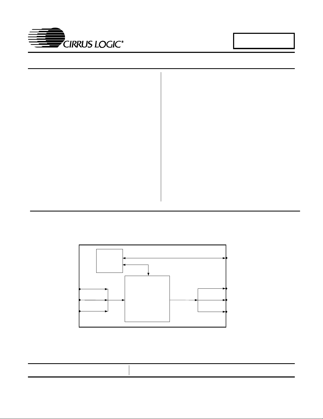
The CDB8427 is designed to allow rapid evaluation of
the CS8427. The board is set up for easy connection to
an Audio Precision or a Rohde and Schwarz test system.
Input and output data formats may independently be set
to either AES/EBU, or S/PDIF with either optical or coaxial physical format.
Separate headers are provided so the Serial Audio Input
Port and Serial Audio Output Port may be interfaced to
off board circuits.
Microsoft
interface to make configuration easy. The software communicates through the PC’s RS232 port to a
microcontroller on the evaluation board that controls the
CS8427. All the possible software modes of the CS8427
may be tested.
ORDERING INFORMATION
®
Windows® 98 PC software provides a GUI
CDB8427 Evaluation Board
Amtel
µC
Optical In
S/PDIF In
AES 3 In
Preliminary Product Information
Cirrus Logic, Inc.
P.O. Box 17847, Austin, Texas 78760
(512) 445 7222 FAX: (512) 445 7581
http://www.cirrus.com
RS232 port to PC
Optical Out
CS8427
S/PDIF Out
AES 3 Out
This document contains information for a new product.
Cirrus Logic reserves the right to modify this product without notice.
Copyright Cirrus Logic, Inc. 2002
(All Rights Reserved)
DS477DB2
AUG ‘02
1
Page 2

TABLE OF CONTENTS
1. OVERVIEW ............................................................................................................................... 3
1.1 CS8427 .............................................................................................................................. 3
1.2 Microcontroller and Memory .............................................................................................. 3
1.3 Crystal Oscillators .............................................................................................................. 3
1.4 RS232 Port ........................................................................................................................ 3
1.5 LED Function Indicators ..................................................................................................... 3
2. CDB8427.EXE QUICK START GUIDE .................................................................................... 4
2.1 Setting up the Hardware ....................................................................................................4
2.2 Installing the Software ........................................................................................................ 4
2.3 Starting up the Software .................................................................................................... 4
2.4 Starting up the Hardware ...................................................................................................4
3. CDB8427.EXE USER'S GUIDE ................................................................................................ 6
3.1 Main Window ..................................................................................................................... 6
3.2 Board Setup ....................................................................................................................... 7
3.3 Script file syntax ................................................................................................................. 7
LIST OF FIGURES
Figure 1. CDB8427 Control Panel Main Window ............................................................................ 6
Figure 2. Board Setup Panel ........................................................................................................... 7
Figure 3. CS8427 Digital Audio Transceiver ................................................................................... 9
Figure 4. Atmel AVR RISC Microcontroller ................................................................................... 10
Figure 5. Power Supplies and Reset Circuit.................................................................................. 11
Figure 6. Silkscreen....................................................................................................................... 12
Figure 7. Top PCB......................................................................................................................... 13
Figure 8. Bottom PCB ................................................................................................................... 14
CDB8427
LIST OF TABLES
Table 1. System Connections ......................................................................................................... 5
Table 2. CDB8427 Jumper Settings................................................................................................5
Table 3. Script file syntax description.............................................................................................. 7
Contacting Cirrus Logic Support
For a complete listing of Direct Sales, Distributor, and Sales Representative contacts, visit the Cirrus Logic web site at:
http://www.cirrus.com/corporate/contacts/sales.cfm
IMPORTANT NOTICE
“Preliminary” product information describes products that are in production, but for which full characterization data is not yet available. “Advance” product information describes products that are in development and subject to development changes. Cirrus Logic, Inc. and its subsidiaries (“Cirrus ”) b elie ve that the in formation contained in this document is accurate and reliable. However, the information is subject to change without notice and is provided “AS IS” without warranty
of any kind (express or implied). Customers are advised to obtain the latest version of relevant information to verify, before placing orders, that information being
relied on is current and complete. All products are sold subject to the terms and conditions of sale supplied at the time of order acknowledgment, including those
pertaining to warranty, patent infringement, and limitation of liability. N o res po nsibility is a ss um ed b y C irrus for the use of this inform a tion, in clu din g use o f this
information as the basis for manufacture or sale of any items, or for infringement of patents or other rights of third parties. This document is the property of Cirrus
and by furnishing this information, Cirrus grants no license, express or implied under any patents, mask work rights, copyrights, trademarks, trade secrets or
other intellectual property rights. Cirrus owns the copyrights of the information contained herein and gives consent for copies to be made of the information only
for use within your organization with respect to Cirrus integrated circuits or other parts of Cirrus. This consent does not extend to other copying such as copying
for general distribution, advertising or promotional purposes, or for creating any work for resale.
An export permit needs to be obtained from the competent authorities of the Japanese Government if any of the products or technologies described in this material and controlled under the “Foreign Exchange and Foreign Trade Law” is to be exported or taken out of Japan. An export license and/or quota needs to be
obtained from the competent authorities of the Chinese Government if any of the products or technologies described in this material is subject to the PRC Foreign
Trade Law and is to be exported or taken out of the PRC.
CERTAIN APPLICATIONS USING SEMICONDUCTOR PRODUCTS MAY INVOLVE POTENTIAL RISKS OF DEATH, PERSONAL INJURY, OR SEVERE
PROPERTY OR ENVIRONMENTAL DAMAGE (“CRITICAL APPLICATIONS”). CIRRUS PRODUCTS ARE NOT DESIGNED, AUTHORIZED, OR WARRANTED TO BE SUITABLE FOR USE IN LIFE-SUPPORT DEVICES OR SYSTEMS OR OTHER CRITICAL APPLICATIONS. INCLUSION OF CIRRUS PRODUCTS
IN SUCH APPLICATIONS IS UNDERSTOOD TO BE FULLY AT THE CUSTOMER'S RISK.
Cirrus Logic, Cirrus, and the Cirrus Logic logo designs are trademarks of Cirrus Logic, Inc. All other brand and product names in this document may be trademarks or service marks of their respective owners.
2
Page 3

1. OVERVIEW
CDB8427
The CDB8427 evaluation board contains a CS8427
and the supporting circuitry necessary for it to operate. The input and output options include AES3
and S/PDIF in optical and coaxial formats. In software mode, the control registers of the CS8427 are
set by an Atmel AVR RISC microcontroller. A Microsoft Windows 98 based program communicates
with the micro through an RS232 port to control the
configuration.
1.1 CS8427
The features and functions of the CS8427 are described in its data sheet.
1.2 Microcontroller and Memory
The functions of the board are controlled by an Atmel AVR RISC microcontroller. The board is
equipped with 512 KBytes of static RAM so that
Channel Status and User bits from the AES stream
may be captured and uploaded to the host PC. The
microcontroller communicates with the CS8427
through its SPI port. The Atmel AVR RISC microcontroller may be bypassed in order to utilize an
external microcontroller through header J10. Header J9 allows the microcontroller on the board to be
programmed with the programmer that is supplied
in the Atmel STK-300 development kit. Additional
software development tools and applications information for the Atmel microcontroller are available
at: http://www.atmel.com.
1.3 Crystal Oscillators
There are positions for two crystal oscillators on
the board. Both locations are equipped with pin
sockets that allow the oscillators to be removed.
The oscillator labeled U10 provides the 6 MHz
clock for the microcontroller and should not be
changed unless you plan on reprogramming the micro.
U3 is the oscillator that provides the Output Master
Clock for the CS8427. The board is shipped with a
12.288 MHz crystal oscillator that can be stuffed at
U3 to set the output sampling rate to 48 kHz.
1.4 RS232 Port
The RS232 port on the upper right hand side of the
board should be connected to the serial port of the
PC running the CDB8427 control software. Follow
the software instructions to properly configure the
serial port for use with the evaluation board.
1.5 LED Function Indicators
LEDs D8 and D9 on the upper right hand corner of
the board allow the user to determine when data is
being transmitted over the RS232 link. The red
LED D4 is the reset indicator and the red LED D1
is connected to the RERR pin of the CS8427. The
two remaining LEDs on the board are not currently
of use to the end user
3
Page 4

CDB8427
2. CDB8427.EXE QUICK START GUIDE
2.1 Setting up the Hardware
Note: SeeTable 1 on page 5 and Table 2 on page 5 for
the configuration and jumper settings.
1) Connect the CDB8427 to a 5 V DC power supply.
2) Set: J11 to Optical, J16 to S/PDIF, enable J13
(S/PDIF), and disable J15 (MUTE).
3) Connect the CDB8427 to the PC COM port using RS232 cable.
4) Apply power to the board.
5) Press the RESET switch (S5).
At this point, the RERR and PROC should be lit.
The hardware is now ready!
2.2 Installing the Software
1) Create a directory called CDB8427 anywhere
on your system.
2) Copy CDB8427.exe into this directory.
3) If you do not already have them, copy the included DLLs msvcrt.dll and mfc42.dll into
your \Windows\System directory.
4) If desired, create a shortcut to CDB8427.exe on
your desktop.
At this point, you are ready to start up the software.
2.3 Starting up the Software
1) Double-click on CDB8427.exe or its shortcut.
2) If you get errors right away, the COM port
needs to be set properly.
3) Click anywhere but inside one of the boxes, this
brings up the Board Setup control panel.
4) Select the COM port you are using to connect
to the CDB8427.
5) Shut down the application, reset the board, and
then restart the application.
2.4 Starting up the Hardware
1) Click anywhere but inside one of the boxes, this
brings up the Board Setup control panel.
2) Click on the Reset button. You should see the
TX and RX leds light up briefly.
3) Click on the AES3 Transmitter tab, then set the
Transmitter data source to AES3 Receiver.
4) Click on the Clock Sources tab, click on
RMCK derived from AES3 input frame and uncheck the Stop Internal Clocks box.
5) Check the performance of the board by doing
an FFT with a -1dBFS 1kHz sine wave for input at 44.1kHz and 48kHz sample rates using
the optical input and optical output.
.
4
Page 5
CDB8427
CONNECTOR INPUT/OUTPUT SIGNAL PRESENT
+5V Input +5 Volt power
GND Input Ground connection from power supply
OPTICAL INPUT Input Digital Audio Interface optical input
S/PDIF INPUT Input Digital Audio Interface coaxial input
AES3 INPUT Input Digital Audio Interface XLR input
RS232 Input/Output Parallel RS232 port for connection to serial port of PC
OPTICAL OUTPUT Output Digital Audio Interface optical output (always enabled)
S/PDIF OUTPUT Output Digital Audio Interface coaxial output
AES3 OUTPUT Output Digital Audio Interface XLR output
J5 Input/Output I/O for RMCLK, ISCLK,ILRCK, and SDIN
J6 Input/Output I/O for OLRCK, OSCLK, OMCK, and SDOUT
J9 Input 10-pin header for external programming of Atmel AVR µC
J10 Input/Output 12-pin header for CS8427 control from external µC
Table 1. System Connections
JUMPER PURPOSE POSITION FUNCTION SELECTED
J11 Selects physical format of digital
audio interface input
J12 Configures AES3 INPUT ENABLE
J13 Configures S/PDIF INPUT ENABLE
J14 Configures OPTICAL INPUT ENABLE
J16 Selects physical format of digital
audio interface output
J17 Configures S/PDFIF OUTPUT ENABLE
J15 Configures HARDWARE MODE
MUTE
Table 2. CDB8427 Jumper Settings
AES3 & S/PDIF
OPTICAL
DISABLE
DISABLE
DISABLE
AES3
S/PDIF
DISABLE
ENABLE
DISABLE
Connects input as either AES3 or S/PDIF
Connects input as OPTICAL
AES3 INPUT enabled
AES3 INPUT disabled
S/PDIF INPUT enabled
S/PDIF INPUT disabled
OPTICAL INPUT enabled
OPTICAL INPUT disabled
Connects output as AES3 XLR
Connects output as S/PDIF coaxial
S/PDIF OUTPUT enabled
S/PDIF OUTPUT disabled
Enables MUTE when in hardware mode 1
Disables MUTE when in hardware mode 1
5
Page 6

CDB8427
3. CDB8427.EXE USER'S GUIDE
3.1 Main Window
The CDB8427 Control Panel allows you to view
and access the data flow configuration of the
CS8427. See Figure 1. Clicking the right mouse
button in any of the boxes will bring up a property
menu containing all the register bits relevant to that
block, as well as some high level functions, such as
data sources and formatting options.
To access additional details about each block, click
the left mouse button on the desired block. This
will display a control panel for the selected block.
If you click outside the boxes, you will bring up the
Board Setup control panel, as shown on the next
page. Note that you can click on any of the tabs to
quickly access that section. Also, any changes you
make in the panel are immediately reflected in the
Main Window, so you may wish to arrange them so
that they do not obscure each other.
Figure 1. CDB8427 Control Panel Main Window
6
Page 7

CDB8427
3.2 Board Setup
The Board Setup panel has some very useful functions, including setting the COM Port used by the
application, resetting the CS8427 from software, as
well as loading/saving register settings into files.
See Figure 2. You can also can read or write any
register on the CS8427 using the CS8427 Register
Access.
3.3 Script file syntax
The setup files generated by the board setup function only record the state of the chip registers.
There are many more useful commands that you
can insert into the setup scripts. Table 1 contains a
short description of these commands with their allowed syntax.
Note: Most commands accept either hexadecimal
(indicated by either a “0x” prefix or “h” suffix) or
decimal parameters.
// used for single line comments
script scriptfile call an external script file named
“scriptfile”
reset 1 assert reset of the CS8427
reset 0 de-assert reset of the CS8427
wr 1 30h write register 1 with hex 30
set RUN 1 set the bit field labeled RUN to 1
write 2 3 0x10
12h 13
Table 3. Script file syntax description
write 3 consecutive registers starting from register 2 with hex 10, hex
12, and decimal 13
Figure 2. Board Setup Panel
7
Page 8

CDB8427
8
Page 9

CDB8427
APMS S/AES
123
R14 6.2K
R13
R12
R11
R10
R9
5
OPT2
4
C3
.1uF
47K
47K
47K
47K
47K
CCLKCDOUT
J2
PHONO-JACK
T2
TRANSFORMER
R16 110
C5
.1uF
5
TP2
TP26
TP27
TP28
CDIN
CCLK
123
TP24
TXP
1 8
R18
TP23
TXN
J16
TP22
H/S
681
VD
4 5
HDR3X1
TP19
TP20
OMCK
DGND
OMCK
TP18
U
6 2
R19
TP16
TP17
OLRCK
SDOUT
INT
SDOUT
84.5
TP15
OSCLK
16181719202122232425262728
OSCLK
OLRCK
123
J17
R21
78
56
132
1000pF
HDR3X1
22K1
J6
3
C41
HDR4X2
4
C8
.1uF
22pF
2
OMCK
C11
J4
OSCLK
OLRCK
SDOUT
+
C14
1
XLR-MALE
VD
L2 FERRITE BEAD
VD
1uF 50V
R24 2 Ohms
C15
+
C17
C16
1uF 50V
.1uF
1000pF
1
78
NC
GNDOut
VD
U3
14
12.888MHz
R26
100
6
VD
INT
SUP4
CEN
H/S
CDIN/CS
SFMT1
/RST
SFMT0
SUP2
SUP1SUP3
TCBLD
C1 .01uF
SUP0 SUP5
MUTE
123
6
CS8427_SPI
U1
CDOUT
/CS
/EMPH
RXP
RXNVAAGND
FILT
/RST
RMCK
RERR
ILRCK
1011121314 15
RMCK
ILRCK
TP7
TP8 TP21
TP9
TP10
TP11
TP12
TP13
TP14
HDR3X1
123
110
J14
123
236
J13
6 2
4 5
123
J11
.1uF
J1
PHONO-JACK
123456789
TP1
TP2
TP3
TP4
TP5
R17
HDR3X1
R15
T1
1 8
TRANSFORMER
C4
TP6
.1uF
R8
47K
R7
47K
R6
47K
R5
47K
R4
47K
R3
47K
R2
47K
R1
47K
L1
47UH
VD
C2
4
OPT1
5
ISCLK
ISCLK
SDIN
SDIN TCBL
1000pF
R20
C6
J12
C9
R22
1.2K
C7
J5
78
56
132
4.7K
.1uF
HDR3X1
123
4.7nF
C12
.1uF
HDR4X2
4
VD
123
J15
C40
HDR3X1
.1uF
C10
HDR3X1
22pF
3
C13
RMCK
ISCLK
ILRCK
SDIN
VA
+
2
1uF 50V
J3
XLR-FEMALE
1
U2A
D1
2 1
R25
74VHC125
2 3
825
LED_R
1
Figure 3. CS8427 Digital Audio Transceiver
9
Page 10

CDB8427
P1
594837261
GNDVD
1516
D5
LED_G
2 1
R30
825
.1uF
C31
.1uF
C30
.1uF
C29
C28
.1uF
C27
.1uF
VD
C26
.1uF
C25
.1uF
+
C24
1uF 50V
+
C23
1uF 50V
U2D
74VHC125
12 11
13
CEN
11 14
S/AES
T1 IN T1 OUT
R1 IN R1 OUT
13 12
VD
MUTE
H/S
SFMT1
D6 1N4148
CONNECTOR DB9
12
12
2
6
V-
V+
U9
C1+
C1-
T2 IN T2 OUT
R2 IN R2 OUT
1
3
8 9
10 7
L4
FERRITE BEAD
SFMT0
D7 1N4148
D8 LED_G
21
21
DS232
C2+
C2-
4
5
R31
2 Ohms
VD
MRST
D9 LED_R
R34
680
R33
680
C39
.1uF
C38
.1uF
C37
.1uF
VD
C36
.1uF
C35
.1uF
C32
+
1
NC
U10
VD
14
C34
C33
78
GNDOut
6.000MHz
R35 100
.1uF
1000pF
1uF 50V
J10
TCBLD
CDIN
CDOUT
1112
CCLK
5678910
/CS
/RESET
INT
1
3
HDR6X2
2
4
SUP1
SUP3
SUP5
SUP2
SUP4
C
9
B
10
A
11
INH
6
Z1
3
Z0
5
Y1
1
Y0
2
X1
13
X0
12
R37 100
132
56
78
910
J9
HDR5X2
SUP0
Figure 4. Atmel AVR RISC Microcontroller
VD
TP32
4
VD
16
15
14
13
12
11
10
9
8
7
6
5
4
3
2
TP30
APMS
TP31
Z
4
Y
15
U11 74HC4053
X
14
/PGM
R36 100
TP29
32
PD1
PD2
PD3
PD4
PD5
PD6
PD7
/WR
33
/RD
34
PC0
35
A8
PC1
36
A9
PC2
37
A10
PC3
38
A11
PC4
39
D7
D6
D5
D4
D3
D2
D1
D0
VD
A12
A13
A[8-14]
A14
D[0-7]
234561789
RN1
PC5
40
PC6
41
PC7
42
ALE
43
PA7(AD7)
44
PA6(AD6)
45
PA5(AD5)
46
PA4(AD4)
47
PA3(AD3)
48
PA2(AD2)
495051525354555657585960616263
8x 47K
A18
A15
31
A17
30
/WE
29
A13
28
A13
A8
27
A8
A9
26
A9
A11
25
A11
/OE
24
A10
23
A10
/CS
22
D7
21
D7
D6
20
D6
D5
19
D5
D4
18
D4
D3
17
D3
Q8
12
Q7
13
Q6
14
Q5
15
Q4
16
Q3
17
Q2
U5 74HC574
18
Q1
19
U6 HM628512
OC
CLK
D8
D7
D6
D5
D4
D3
D2
D1
2
A14
3
A14
A12
4
A12
A7
5
A6
6
A5
7
A4
8
A3
9
A2
10
A1
11
A0
12
D0
13
D0
D1
14
D1
D2
15
D2
1
11
9
D7
8
D6
7
D5
6
D4
5
D3
4
D2
3
D1
2
D0
1
A16
OC
1
C
11
Q8
D8
Q7
Q6
Q5
Q4
Q3
Q2
Q1
U7 74HC573
9
D7
8
D6
7
D5
6
D4
5
D3
4
D2
3
D1
2
12
13
14
15
16
17
18
19
PA1(AD1)
PA0(AD0)VDGND
VD
S6
PD0/INT0
U8
PF7(ADC7)
PF6(ADC6)
PF5(ADC5)
9
8
VD
GND
XTAL2
XTAL1
ATmega103
PF4(ADC4)
PF3(ADC3)
PF2(ADC2)
PF1(ADC1)
/RST
TOSC2
TOSC1
PF0(ADC0)
AREF
AGND
16151413121110
1234567
171819202122232425262728293031
PB7
AVCC
64
21
D10
R32 1K
SW DIP-8
VD
PB6
PB5
PB4
PB3/CDOUT
PB2/CDIN
PB1/CCLK
PB0/CS
PE7
PE6
PE5
PE4
PE3
PE2
PE1/TXD
PE0/RXD
/PEN
LED_G
10
Page 11

/RST
VD
CDB8427
LED_R
D4
2
R29
825
1
VA
VD
/RESET
D2
R28
BAT85
U2B
47K
1 2
74VHC125
5 6
4
BAT85
D3
12
VD
/PGM
U2C
74VHC125
D11
10
9 8
2
MRST
BAT85
1
C19
C18
+
R27
.1uF
100uF 6.3V
2 Ohms
L3
FERRITE BEAD
C22
C21
.1uF
C20
100uF 6.3V
+
Z1
P6KE6.8A
1 2
RED
1
J8
1
J7
VD
BLACK
R38
10K
S5
.01uF
SW_MOM
1 3
5
11
Figure 5. Power Supplies and Reset Circuit
Page 12

CDB8427
Figure 6. Silkscreen
12
Page 13

CDB8427
Figure 7. Top PCB
13
Page 14

CDB8427
Figure 8. Bottom PCB
14
 Loading...