

Page 1
Evaluation Board for CS8422
CS8406
CS8422
RX Input
TX Output
Canned
Oscillator
Crystal
Oscillator
Jumper
ILRCK
ISCLK
SDIN
Mux
XTI
FPGA
OLRCK2
OSCLK2
SDOUT2
ILRCK
ISCLK
SDIN
OMCK
Header
Header
Resistors
Hardware
Switches
Header
RMCK
USB Micro-
controller
I2C/SPI
OLRCK1
OSCLK1
SDOUT1
TDM_IN
Reset
Canned
Oscillator
Header
Reset
USB
CDB8422
Features
IEC-60958, AES3/EBU, S/PDIF Inputs
– Single-Ended Inputs via Optical and RCA
Input Jacks
– Differential Inputs via XLR Input Jack
S/PDIF Outputs
– Optical and RCA Output Jacks
– CS8406 Digital Audio Transmitter
I/O Stake Headers
– External Control Port Accessibility
– External Serial Audio I/O Accessibility
3.3 V Logic Interface
Powered by Single External Power Supply or
PC USB Port Connection
H/W Control via DIP Switches
FlexGUI S/W Control - Windows
– Pre-Defined & User-Configurable Scripts
®
Compatible
Description
Using the CDB8422 evaluation board is an ideal way to
evaluate the CS8422. Use of the board requires a digital
signal source, an analyzer, and a power supply. A Windows
PC-compatible computer is also required if using
software mode to configure the CDB8422.
S/PDIF and AES3/EBU input connections are made via
RCA phono, optical, or XLR connectors to the CS8422.
S/PDIF output connections are made via RCA phono or
optical connectors from the CS8406 (S/PDIF Tx). System timing can be provided by a S/PDIF or AES3/EBU
input signal, by the CS8422 with supplied master clock,
or by an I/O stake header with a DSP connected.
The provided Windows-based software GUI makes
configuring the CDB8422 easy. The software communicates through the PC’s USB port to configure the board
so that all features of the CS8422 can be evaluated.
The board may also be configured without a PC connection by using hardware switches; however, not all
configurations of the CDB8422 are possible in hardware mode.
ORDERING INFORMATION
CDB8422 Evaluation Board
http://www.cirrus.com
Copyright Cirrus Logic, Inc. 2010
(All Rights Reserved)
MAY '10
DS692DB2
Page 2

TABLE OF CONTENTS
1. SYSTEM OVERVIEW ............................................................................................................................. 4
1.1 Power ............................................................................................................................................... 4
1.2 Grounding and Power Supply Decoupling ....................................................................................... 4
1.3 FPGA ............................................................................................................................................... 4
1.4 CS8422 ............................................................................................................................................ 4
1.5 CS8406 Digital Audio Transmitter .................................................................................................... 5
1.6 CS8422 XTI Sources ....................................................................................................................... 5
1.7 I/O Stake Headers ........................................................................................................................... 5
1.8 S/PDIF and AES3/EBU Inputs ......................................................................................................... 5
2. SOFTWARE MODE ................................................................................................................................ 6
2.1 Quick Start Guide ............................................................................................................................. 6
2.2 Configuration Options ...................................................................................................................... 7
2.2.1 S/PDIF In to S/PDIF and PCM Out ......................................................................................... 7
2.2.2 AES3/EBU In to S/PDIF and PCM Out ................................................................................... 8
2.2.3 PCM In to S/PDIF and PCM Out .............................................................................................9
2.2.4 TDM In to TDM Out ............................................................................................................... 10
2.3 Software Mode Control .................................................................................................................. 11
2.3.1 CS8422 Main Setup Tab ....................................................................................................... 12
2.3.2 CS8422 Receiver Controls and Status Tab .......................................................................... 13
2.3.3 CS8422 Interrupt Controls and Status Tab ........................................................................... 14
2.3.4 FPGA Controls Tab ............................................................................................................... 15
2.3.5 Register Maps Tab ................................................................................................................ 16
2.4 FPGA Register Quick Reference ................................................................................................... 17
2.5 FPGA Register Descriptions .......................................................................................................... 17
2.5.1 Code Revision ID (Address 01h) - Read Only ....................................................................... 17
2.5.2 MCLK Control (Address 02h) ................................................................................................ 17
2.5.2.1 SAO2 HDR MCLK Source (SAO2_Mclk) ................................................................... 17
2.5.2.2 SAO1 HDR and CS8406 MCLK Source (SAO1_Mclk) .............................................. 17
2.5.2.3 AUX MCLK Source (AUX_Mclk) ................................................................................ 18
2.5.2.4 CS8422 Reset Pin (DUT_RST) ................................................................................. 18
2.5.3 Subclock Control (Address 03h) ............................................................................................ 18
2.5.3.1 TDM Header Subclock Source (TDM_SEL) .............................................................. 18
2.5.3.2 SAI Subclock Source (SAI_MS) ................................................................................ 18
2.5.3.3 SAO2 Subclock Source (SAO2_MS) ......................................................................... 19
2.5.3.4 SAO1 Subclock Source (SAO1_MS) ......................................................................... 19
2.5.4 CS8406 Control 1 (Address 04h) .......................................................................................... 19
2.5.4.1 OMCK/ILRCK Ratio (HWCK) ..................................................................................... 19
2.5.4.2 Validity Bit (VBIT_IN) .................................................................................................19
2.5.4.3 User Data (UBIT_IN) ................................................................................................. 20
2.5.4.4 TCBL (TCBL) ............................................................................................................. 20
2.5.4.5 C BIT (CBIT_INT) ...................................................................................................... 20
2.5.4.6 Interface Format (SFMT) ........................................................................................... 20
2.5.5 CS8406 Control 2 (Address 05h) .......................................................................................... 21
2.5.5.1 CS8406 Reset Pin (8406_RST) ................................................................................. 21
2.5.5.2 AUDIO Bit (AUDIOb) ................................................................................................. 21
3. HARDWARE MODE ............................................................................................................................. 22
3.1 Quick Start Guide ........................................................................................................................... 22
3.2 Configuration Options .................................................................................................................... 23
3.2.1 AES3/EBU In to S/PDIF and PCM Out ................................................................................. 23
3.2.2 TDM In to TDM Out ............................................................................................................... 24
3.3 Hardware Mode Control ................................................................................................................. 25
4. SYSTEM CONNECTIONS ........................................................................................................
CDB8422
........... 28
2 DS692DB2
Page 3

5. JUMPER SETTINGS ........................................................................................................................... 29
6. LEDS .................................................................................................................................................... 29
7. CDB8422 BLOCK DIAGRAM .............................................................................................................. 30
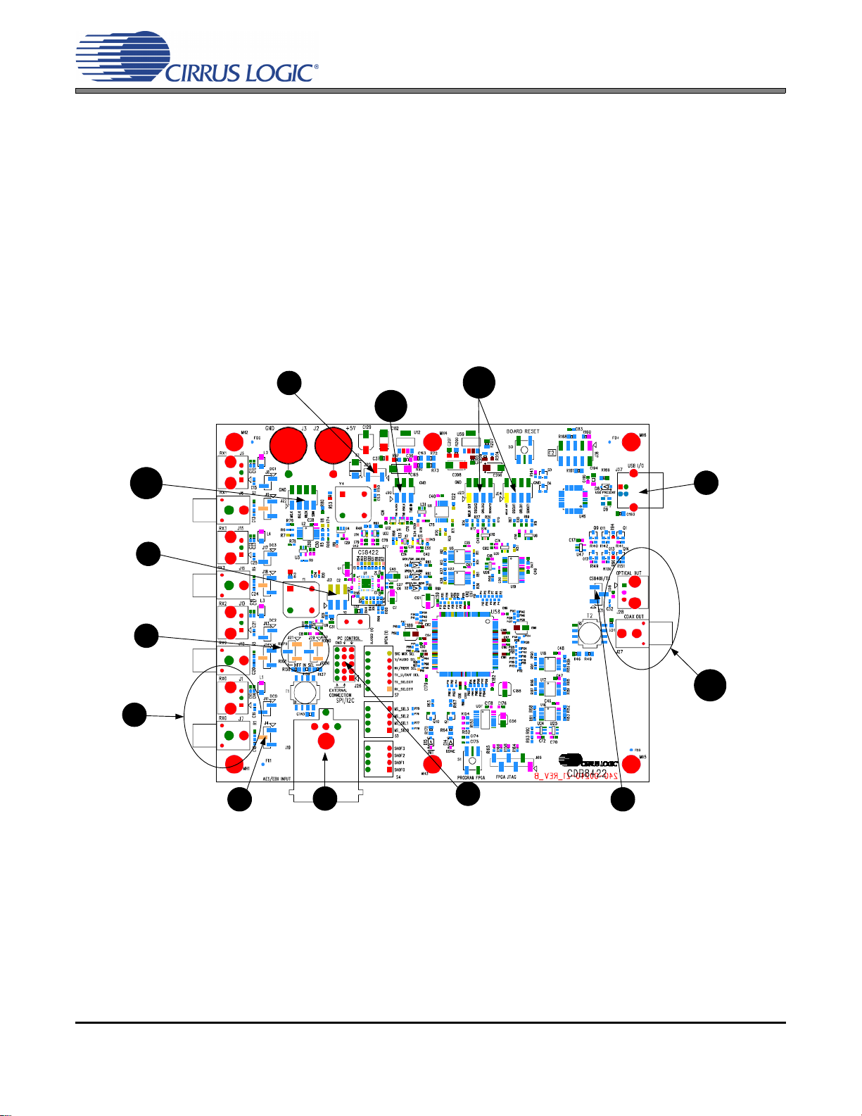
8. CDB8422 SCHEMATICS ...................................................................................................................... 31
9. CDB8422 LAYOUT ............................................................................................................................... 43
10. REVISION HISTORY .......................................................................................................................... 46
LIST OF FIGURES
Figure 1.Software Mode Quick Start Guide ................................................................................................ 6
Figure 2.S/PDIF In to S/PDIF and PCM Out ............................................................................................... 7
Figure 3.AES3/EBU In to S/PDIF and PCM Out ......................................................................................... 8
Figure 4.PCM In to S/PDIF and PCM Out ................................................................................................... 9
Figure 5.TDM In to TDM Out ..................................................................................................................... 10
Figure 6.CS8422 Main Setup Tab ............................................................................................................. 12
Figure 7.CS8422 Receiver Controls and Status Tab ................................................................................ 13
Figure 8.CS8422 Interrupt Controls and Status Tab ................................................................................. 14
Figure 9.FPGA Controls Tab ..................................................................................................................... 15
Figure 10.Register Maps Tab - CS8422 ................................................................................................... 16
Figure 11.Hardware Mode Quick Start Guide ........................................................................................... 22
Figure 12.AES3/EBU In to S/PDIF and PCM Out ..................................................................................... 23
Figure 13.TDM In to TDM Out ................................................................................................................... 24
Figure 14.Block Diagram ........................................................................................................................... 30
Figure 15.CS8422 & XTI (Schematic Sheet 1) ......................................................................................... 31
Figure 16.RX Inputs (Schematic Sheet 2) ................................................................................................. 32
Figure 17.PCM Input Header (Schematic Sheet 3) ................................................................................... 33
Figure 18.HW Mode Control (Schematic Sheet 4) .................................................................................... 34
Figure 19.FPGA (Schematic Sheet 5) ....................................................................................................... 35
Figure 20.MCLK Routing (Schematic Sheet 6) ......................................................................................... 36
Figure 21.Serial Audio 1 Output Header (Schematic Sheet 7) ................................................................. 37
Figure 22.Serial Audio 2 Output Header (Schematic Sheet 8) ................................................................. 38
Figure 23.TDM Header (Schematic Sheet 9) ............................................................................................ 39
Figure 24.CS8406 and Auxiliary TX (Schematic Sheet 10) ...................................................................... 40
Figure 25.USB and MCU (Schematic Sheet 11) ....................................................................................... 41
Figure 26.Power (Schematic Sheet 12) .................................................................................................... 42
Figure 27.Silk Screen ................................................................................................................................ 43
Figure 28.Top-Side Layer ......................................................................................................................... 44
Figure 29.Bottom-Side Layer .................................................................................................................... 45
CDB8422
LIST OF TABLES
Table 1. Switch Settings - AES3/EBU In to S/PDIF and PCM Out ........................................................... 23
Table 2. Switch Settings - TDM In to TDM Out ......................................................................................... 24
Table 3. S3 Settings .................................................................................................................................. 25
Table 4. S4 Settings .................................................................................................................................. 26
Table 5. S7 Settings .................................................................................................................................. 27
Table 6. System Connections ................................................................................................................... 28
Table 7. Jumper Settings .......................................................................................................................... 29
Table 8. LEDs ........................................................................................................................................... 29
DS692DB2 3
Page 4

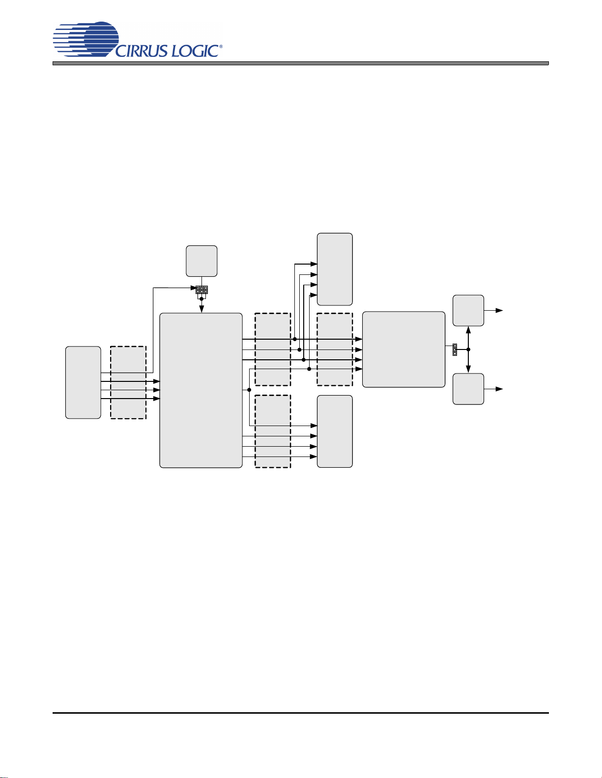
1. SYSTEM OVERVIEW
CDB8422
The CDB8422 platform provides S/PDIF and AES3/EBU digital interfaces to the CS8422 and allows for external
DSP and I²C
power supply of +5 V can be used to provide power for the CDB8422. Optionally, the evaluation board may be powered from a USB connection, which also serves as an interface to a PC. The CDB8422 is configured in software
mode using Cirrus Logic’s Windows-compatible FlexGUI software to read/write to device registers. In hardware
mode, the evaluation board is configured using several DIP switches.
This section describes the various components on the CDB8422 and how they are used. The two following sections
(Section 2 and Section 3) provide details on operating the CDB8422 in software and hardware mode, respectively.
Both sections begin with a simplified quick connect guide provided for user convenience which can be used to set
up the board quickly with the CS8422 in its startup default configuration. Next, descriptions are given for several
useful configuration options in which the board can be used. Then, complete configuration details for each mode
are described. Section 4, Section 5, and Section 6 provide a description of all stake headers, connectors, and LEDs
on the board, including the default factory settings for all jumpers. The CDB8422 schematic and layout set is shown
in Figures 15 through 29.
®
or SPITM control port interconnects. On-board voltage regulators are provided so that a single external
1.1 Power
Power and ground is supplied to the evaluation board via binding posts J2 and J3 (respectively) or the USB
connection J37. Jumper J20 allows the user to select the power source (see Section 5 for details). The voltage connected to the binding posts should be +5 V. An on-board voltage regulator provides +3.3 V for the
CS8422’s VA, VL, and V_REG supplies. All voltage inputs are referenced to ground using the black binding
post J3.
1.2 Grounding and Power Supply Decoupling
The CDB8422 demonstrates the optimal power supply and grounding arrangements for the CS8422.
Figure 14 provides an overview of the connections to the CS8422. Figure 27 shows the component place-
ment, Figure 28 shows the top layout, and Figure 29 shows the bottom layout. Power supply decoupling capacitors are located as close as possible to the CS8422. Extensive use of ground plane fill helps reduce
radiated noise.
1.3 FPGA
The FPGA controls digital signal routing between the CS8422, the CS8406, and the I/O stake headers. It
also provides routing control of the system master clock from an on-board canned oscillator, an on-board
crystal oscillator, and the CS8422. The FPGA configures the CDB8422 in hardware mode and routes serial
control signals from the micro controller to the CS8422 in software mode. The Cirrus FlexGUI software provides full control of the FPGA’s routing and configuration options, see Section 2.3, Section 2.4, and Section
2.5 for details. A subset of the FPGA’s options are accessible in hardware mode using DIP switches, see
Section 3.3 for details.
1.4 CS8422
A complete description of the CS8422 can be found in the CS8422 product data sheet.
When the evaluation board is connected to a PC via the USB connector, the CS8422 is placed in software
mode and is configured using the Cirrus FlexGUI. The device configuration registers are accessible via the
“Register Maps” tab of the Cirrus FlexGUI software. This tab provides low-level control of each bit. For easier configuration, additional tabs provide high-level control. Section 2.3 provides configuration details.
4 DS692DB2
Page 5

When the evaluation board is not connected to a PC, the CS8422 is placed in hardware mode and is configured using DIP switches. Certain switch settings require a board reset to take affect, see Section 3.3 for
more information.
1.5 CS8406 Digital Audio Transmitter
A complete description of the CS8406 transmitter and a discussion of the digital audio interface can be
found in the CS8406 data sheet.
The CS8406 converts the output PCM data stream from the CS8422 into S/PDIF data that is output to the
optical (J28) and RCA (J27) connectors. In software mode, device configuration pins are controlled by using
the “FPGA Controls” tab of the Cirrus FlexGUI software, see Section 2.3 for details.
1.6 CS8422 XTI Sources
The CS8422 XTI clock source is selected by jumper J23. The clock signal may be provided by the socketed
on-board canned oscillator (Y1), socketed on-board parallel resonant crystal (Y2), or input serial header
J22. The oscillator and crystal are mounted in pin sockets, allowing for easy removal and replacement. The
device footprint on the board for Y1 will only accommodate half-can-sized oscillators. Section 5 describes
which jumper position selects each clock source.
1.7 I/O Stake Headers
CDB8422
The evaluation board has been designed to allow interfacing with external systems via several serial port
headers and a control port header (J26). The input serial port header (J22) provides access to the input serial audio port of the CS8422. The output serial port headers provide access to both output serial audio
port 1 (J24) and output serial audio port 2 (J25) of the CS8422. All three serial port headers can be placed
in master or slave mode with respect to the CS8422. The TDM input header (J30) allows TDM data to be
input from another system into the CS8422.
The control port header provides bidirectional access to the I²C or SPI control port signals by simply removing all the shunts from the “PC Control” position. The user may then connect a ribbon cable connector to
the “External Connection” pins for external control of board functions. A single row of “GND” pins is provided
to maintain signal ground integrity. Two unpopulated pull-up resistors are also available should the user
choose to use the CDB8422 logic supply (VL) externally.
1.8 S/PDIF and AES3/EBU Inputs
The CDB8422 allows for both S/PDIF and AES3/EBU input signals to be connected to the CS8422. Four
pairs of optical and RCA connectors are provided to connect single-ended S/PDIF signals to the four receiver ports on the CS8422. A single XLR connector is provided to connect a differential AES3/EBU signal to
either of the two differential receiver ports on the CS8422.
Figure 16 illustrates how the S/PDIF and AES3/EBU inputs are connected and routed. Table 7 details the
associated jumper selections. The CS8422 data sheet specifies the maximum allowed input voltage levels.
Note that, as a result of signal attenuation resulting from PCB parasitics, the input S/PDIF signal amplitude
at the receiver input pins of the CS8422 may be lower than at the input connectors. See the CS8422 data
sheet for the minimum signal amplitude required at the receiver input pins of the CS8422.
DS692DB2 5
Page 6
CDB8422
Shunt right 2 pins of J20
to receive power from
USB +5 V DC power.
Connect USB to board.
Open Flex GUI software
on PC and load quick
setup script.
*See section 2.2 for
quick setup descriptions.
Provide S/PDIF
input to board via
J1 or J7.
PCM digital audio
input can be provided
to the board via
header J22.
1
7
8
PCM digital audio output can be
received from the board via
headers J24 and J25.
Shunt top 2 pins on J4
if using optical input
J1. Shunt bottom 2
pins on J4 if using
coaxial input J7.
4
Shunt the right 2 pins on all rows.
Connect a ribbon cable to left 2
pins of all rows if external system
connect is required.
5
Shunt the middle
2 pins on J23.
2
Receive S/PDIF
output from board
via J28 or J27.
Shunt the top 2 pins
on J31.
6
AES3/EBU input
can also be
provided to the
board via J19.
9
Shunt the top 2 pins on
J21 and J29.
3
TDM input can be
provided to the board via
header J30.
10
11
12
13
2. SOFTWARE MODE
Connecting a USB port cable from a PC to the USB connector (J37) on the CDB8422 and launching the provided
graphical user interface (Cirrus Logic FlexGUI) software enables one to use the board in software mode. The GUI
for the CDB8422 allows the user to configure the CS8422 and FPGA registers via the on-board I²C or SPI control
bus.
2.1 Quick Start Guide
Figure 1 below is a simplified quick start up guide made for user convenience. The user may choose from
steps 8 through 13 depending on the desired measurement. Refer to Section 2.2 for details on how the var-
ious components on the board interface with each other in different board configurations. Refer to Section
2.3 for descriptions on control settings in the Cirrus FlexGUI software.
Figure 1. Software Mode Quick Start Guide
6 DS692DB2
Page 7
2.2 Configuration Options
CS8422
CS8406
S/PDIF Tx
Optical
S/PDIF In
(SLAVE)
J1
OR
RX0
Buffer Buffer
Header
J24
Buffer
Header
J25
(MASTER)
(MASTER)
J7
J4
Coaxial
S/PDIF In
OSCL K1
OLRC K1
SDOUT1
OSCL K2
OLRC K2
SDOUT2
ISCLK
ILRCK
SDIN
OSCLK2
OLRCK2
SDOUT2
OSCLK1
OLRCK1
SDOUT1
Optical
S/PDIF
Out
J28
AND
J27
J31
Coaxial
S/PDIF
Out
S/PDIF
OUT
RMCK
OMCK
MCLK OUT
MCLK OUT
PCM Out
through SRC
PCM Out
no SRC
In software mode, to configure the CDB8422 for making performance measurements, one needs to use Cirrus Logic’s Windows compatible FlexGUI software to program the various components on the board. This
section serves to give a deeper understanding of the on-board circuitry and the digital clock and data signal
routing involved in several common software mode configurations of the CDB8422. These scripts only serve
as a starting point; after loading a script, the GUI can be further configured as needed (clock ratios, serial
formats, etc).
2.2.1 S/PDIF In to S/PDIF and PCM Out
The CS8422’s S/PDIF receiver and SRC output performance can be tested by loading the “SPDIF In to
SPDIF and PCM Out” quick setup file provided with the software package. The script configures the dig-
ital clock and data signal routing on the board as shown in Figure 2.
Digital S/PDIF input can be provided on the optical (J1) or RCA (J7) jacks. Jumper J4 selects which input
signal is connected to the RX0 pin of the CS8422. The script configures the CS8422’s internal circuitry to
send the input audio data through its SRC to serial output port 1. This data is presented as PCM audio at
header J24 and S/PDIF audio at J27 (coaxial) and J28 (optical). The input data is also passed through
(SRC is bypassed) to serial output port 2. This data is presented as PCM audio at header J25. Refer to
Section 2.3 for details on software configuration.
CDB8422
Figure 2. S/PDIF In to S/PDIF and PCM Out
DS692DB2 7
Page 8
2.2.2 AES3/EBU In to S/PDIF and PCM Out
CS8422
CS8406
S/PDIF Tx
(SLAVE)
Buffer Buffer
Header
J24
Buffer
Header
J25
(MASTER)
(MASTER)
OSCLK 1
OLRCK1
SDOUT1
OSCLK 2
OLRCK2
SDOUT2
ISCLK
ILRCK
SDIN
OSCL K2
OLRCK2
SDOUT2
OSCL K1
OLRCK1
SDOUT1
Optical
S/PDIF
Out
J28
AND
J27
J31
Coaxial
S/PDIF
Out
S/PDIF
OUT
RMCK
OMCK
MCLK OUT
MCLK OUT
J19
J21
AES3/EBU
In
J29
RXP0
RXP1
RXN0
RXN1
PCM Out
through SRC
PCM Out
no SRC
The CS8422’s AES3/EBU receiver and SRC output performance can be tested by loading the “AES3 In
to SPDIF and PCM Out” quick setup file provided with the software package. The script configures the
digital clock and data signal routing on the board as shown in Figure 3.
Digital AES3/EBU input is provided by the XLR jack J19 to the RXP0 and RXN0 pins of the CS8422. The
script configures the CS8422’s internal circuitry to send the input audio data through its SRC to serial output port 1. This data is presented as PCM audio at header J24 and S/PDIF audio at J27 (coaxial) and J28
(optical). The input data is also passed through (SRC is bypassed) to serial output port 2. This data is
presented as PCM audio at header J25. Refer to Section 2.3 for details on software configuration.
CDB8422
Figure 3. AES3/EBU In to S/PDIF and PCM Out
8 DS692DB2
Page 9
2.2.3 PCM In to S/PDIF and PCM Out
CS8406
S/PDIF Tx
(SLAVE)
Buffer Buffer
Header
J24
Buffer
Header
J25
(MASTER)
(MASTER)
OSCLK1
OLRCK1
SDOUT1
OSCLK2
OLRCK2
SDOUT2
ISCLK
ILRCK
SDIN
OSCLK2
OLRCK2
SDOUT2
OSCLK1
OLRCK1
SDOUT1
Optical
S/PDIF
Out
J28
AND
J27
J31
Coaxial
S/PDIF
Out
S/PDIF
OUT
RMCK
OMCK
MCLK OUT
MCLK OUT
CS8422
J23
XTI
Y1
ISCLK
ILRCK
SDIN
Buffer
(SLAVE)
PCM In
MCLK
ISCLK
ILRCK
Header
J22
SDIN
PCM Out
through SRC
PCM Out
no SRC
The CS8422’s serial input port and SRC output performance can be tested by loading the “PCM In to
SPDIF and PCM Out” quick setup file provided with the software package. The script configures the digital clock and data signal routing on the board as shown in Figure 4.
PCM audio input is provided by the PCM input header J22. The jumper position on J23 may be changed
to use the MCLK signal from J22 for the CS8422’s XTI signal. The script configures the CS8422’s internal
circuitry to send the input audio data through its SRC to serial output port 1. This data is presented as
PCM audio at header J24 and S/PDIF audio at J27 (coaxial) and J28 (optical). The input data is also
passed through (SRC is bypassed) to serial output port 2. This data is presented as PCM audio at header
J25. Refer to Section 2.3 for details on software configuration.
CDB8422
Figure 4. PCM In to S/PDIF and PCM Out
DS692DB2 9
Page 10
2.2.4 TDM In to TDM Out
CS8422
Optical
S/PDIF In
J1
OR
RX0
Buffer
Header
J24
Buffer
Header
J25
(MASTER)
(MASTER)
J7
J4
Coaxial
S/PDIF In
OSCLK1
OLRCK1
SDOUT1
OSCLK2
OLRCK2
SDOUT2
OSCLK2
OLRCK2
SDOUT2
OSCLK1
OLRCK1
SDOUT1
XTI
J23
Y1
Header
J30
TDM
OSCLK
TDM
OLRCK
TDM IN
Buffer
TDM
Out
TDM_IN
TDM
In
PCM Out
no SRC
RMCK
MCLK OUT
MCLK OUT
GPO3
(XTI)
The CS8422’s TDM output performance can be tested by loading the “TDM In to TDM Out” quick setup
file provided with the software package. The script configures the digital clock and data signal routing on
the board as shown in Figure 5.
TDM audio input data is provided by the TDM input header J30. The LRCK and SCLK signals located at
header J30 should be used to clock in the input TDM data. Optionally, digital S/PDIF input can be provided
on the optical (J1) or RCA (J7) jacks. Jumper J4 selects which input signal is connected to the RX0 pin of
the CS8422. The script configures the CS8422’s internal circuitry to multiplex the TDM input and S/PDIF
input data together and send the output data to serial output port 1. This data is presented as TDM audio
at header J24. The S/PDIF input data is also passed through (not multiplexed) to serial output port 2. This
data is presented as PCM audio at header J25. Refer to Section 2.3 for details on software configuration.
CDB8422
Figure 5. TDM In to TDM Out
10 DS692DB2
Page 11
2.3 Software Mode Control
The CDB8422 may be used with the Microsoft® Windows®-based FlexGUI graphical user interface, allowing software control of the CS8422 and FPGA registers. The latest control software may be downloaded
from www.cirrus.com/msasoftware. Step-by-step instructions for setting up the FlexGUI are provided as follows:
1. Download and install the FlexGUI software as instructed on the Website.
2. Connect the CDB to the host PC using a USB cable (make sure pin 1 and pin 2 of J20 are shunted).
3. Launch the Cirrus FlexGUI. Once the GUI is launched successfully, all registers are set to their default
reset state.
4. Refresh the GUI by clicking on the “Update All Devices” button. The default state of all registers are now
visible.
For standard set-up:
5. Set up the CS8422 in the “CS8422 Main Setup”, “CS8422 Receiver Controls and Status”, and “CS8422
Interrupt Controls and Status” tabs as desired.
6. Set up the FPGA and CS8406 in the “FPGA Controls” tab as desired.
7. Begin evaluating the CS8422.
CDB8422
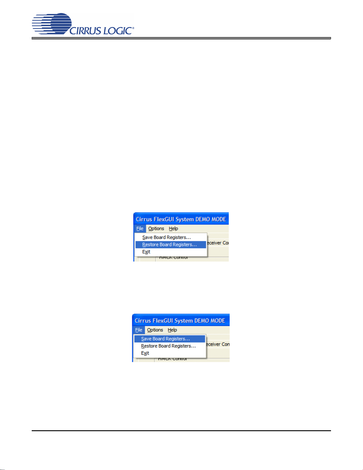
For quick set-up, the CDB8422 may, alternatively, be configured by loading a predefined sample script file:
8. On the File menu, click "Restore Board Registers..."
9. Browse to Boards\CDB8422\Scripts\.
10. Choose any one of the provided scripts to begin evaluation.
To create personal scripts files:
11. On the File menu, click "Save Board Registers..."
12. Enter any name that sufficiently describes the created setup.
13. Choose the desired location and save the script.
14. To load this script, follow the instructions from step 8 above.
DS692DB2 11
Page 12
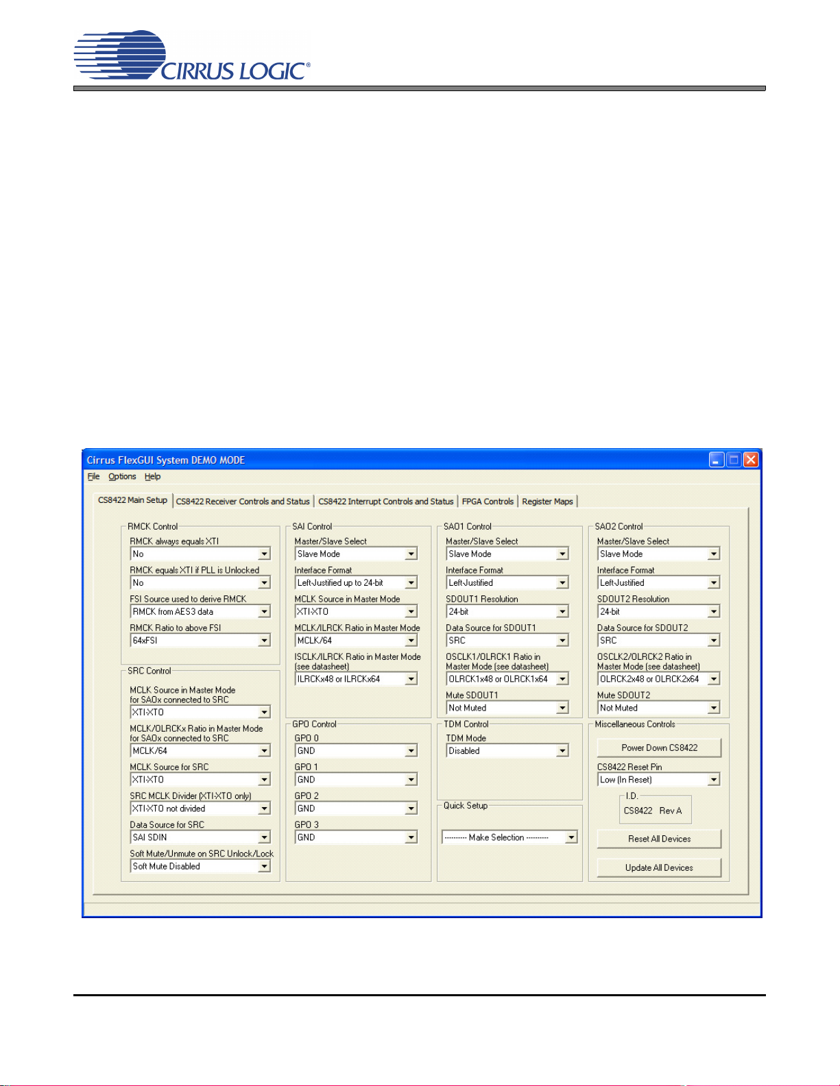
2.3.1 CS8422 Main Setup Tab
Figure 6. CS8422 Main Setup Tab
The “CS8422 Main Setup” tab provides high-level control of the serial port related registers within the
CS8422. A description of each control group is outlined below. See the CS8422 data sheet for complete
register descriptions.
RMCK Control - Configures the CS8422’s RMCK source and behavior.
SAI Control - Configures the serial audio input port of the CS8422.
SAO1 and SAO2 Control - Configures the two serial audio output ports of the CS8422.
SRC Control - Configures the CS8422’s sample rate converter (SRC).
GPO Control - Specifies the signals located on each of the four GPO pins of the CS8422.
TDM Control - Enables TDM Mode on either serial audio output port of the CS8422.
Quick Setup - Loads register settings for preset configurations of the CDB8422, see Section 2.2.
Miscellaneous Controls - Controls the power-down bit of CS8422, resets to return either the CS8422 or
CDB8422 to default setup, and an update button to read all registers and reflect the current values in the
GUI.
CDB8422
12 DS692DB2
Page 13
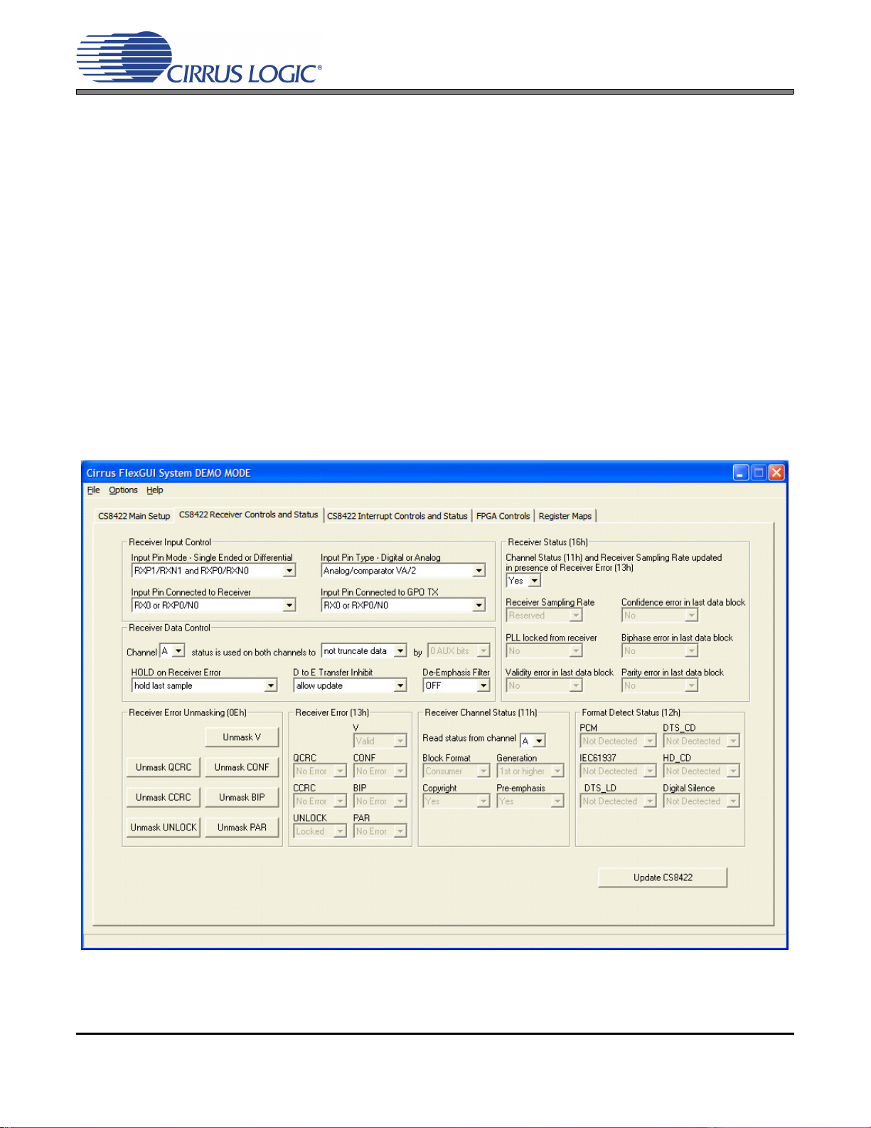
2.3.2 CS8422 Receiver Controls and Status Tab
Figure 7. CS8422 Receiver Controls and Status Tab
The “CS8422 Receiver Controls and Status” tab provides high-level control of the CS8422’s S/PDIF receiver register settings. A description of each group is outlined below. See the CS8422 data sheet for
complete register descriptions.
Receiver Input Control - Configures the CS8422’s receiver input pins and mux.
Receiver Data Control - Configures the CS8422’s receiver data processing.
Receiver Error Unmasking - Configures the CS8422’s receiver error unmasking.
Receiver Error - Shows the status for the CS8422’s unmasked receiver errors.
Receiver Channel Status - Shows the status bits for the CS8422’s selected receiver channel.
Receiver Status - Shows CS8422’s receiver errors occurring within last input data block.
Receiver Format Detect Status - Shows the data format detected on the CS8422’s receiver.
Update CS8422 - Reads all registers in the CS8422 and reflects the current values in the GUI.
CDB8422
DS692DB2 13
Page 14
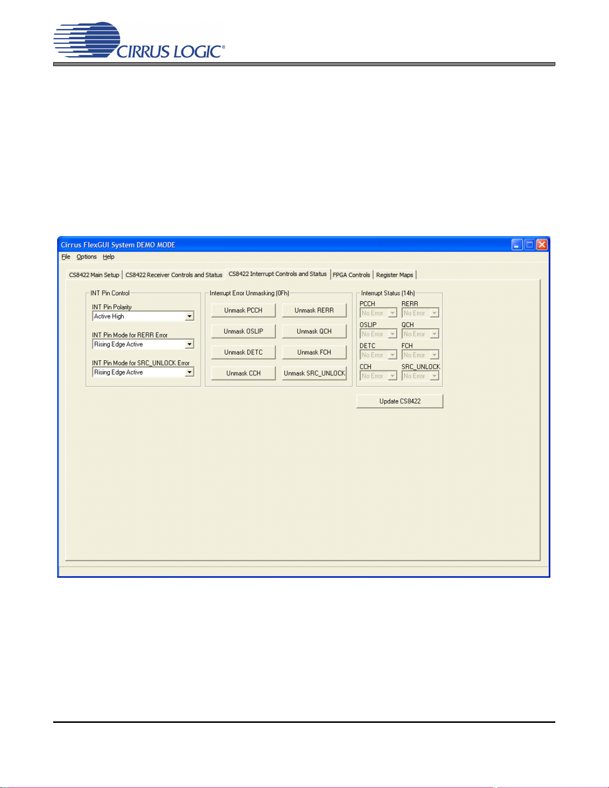
2.3.3 CS8422 Interrupt Controls and Status Tab
Figure 8. CS8422 Interrupt Controls and Status Tab
The “CS8422 Interrupt Controls and Status” tab provides high-level control of the CS8422’s interrupt pin
register settings. A description of each control group is outlined below. See the CS8422 data sheet for
complete register descriptions.
INT Pin Control - Controls the CS8422’s INT pin polarity and modes.
Interrupt Error Unmasking - Controls the CS8422’s interrupt error unmasking to affect the INT pin.
Interrupt Status - Shows the status of CS8422’s unmasked interrupt errors.
Update CS8422 - Reads all registers in the CS8422 and reflects the current values in the GUI.
CDB8422
14 DS692DB2
Page 15

2.3.4 FPGA Controls Tab
Figure 9. FPGA Controls Tab
The “FPGA Controls” tab provides high-level control of the on-board FPGA’s register settings. This tab
provides controls for MCLK and subclock routing between devices on the CDB8422. Controls for the
CS8406 S/PDIF transmitter are also provided. A description of each control group is outlined below.
MCLK Routing - Specifies MCLK source for both serial audio output port headers on the board.
Subclock Routing - Controls bidirectional buffers to determine subclock signal direction between the
CS8422 and serial I/O interface headers. Make sure the CS8422 is also configured to properly output subclocks in master mode or receiver subclocks in slave mode for each serial port.
CS8422 Controls - The state of the CS8422 reset pin may be set.
CS8406 Controls - Controls CS8406 settings and reset pin state.
Reset FPGA - Returns the FPGA and CS8422 to their default setup.
Update FPGA - Reads all registers in the FPGA and reflects the current values in the GUI.
CDB8422
DS692DB2 15
Page 16

2.3.5 Register Maps Tab
Figure 10. Register Maps Tab - CS8422
The Register Maps tabs provide low-level control of the CS8422, FPGA, and GPIO register settings. Register values can be modified bit-wise or byte-wise. “Left-clicking” on a particular register accesses that register and shows its contents at the bottom. The user can change the register contents by using the pushbuttons, by selecting a particular bit and typing in the new bit value, or by selecting the register in the map
and typing in a new hex value. The communication mode of the CS8422 (I²C or SPI) may be selected as
well. See Section 2.5 for details on each register setting of the FPGA. If the CS8422’s configurable I²C
address bits (AD1 or AD0) are modified in the GPIO tab, the FPGA and CS8422 will be reset. The
CS8422’s AD2 bit is always set to zero (GPO2 has no pull-up resistor).
CDB8422
16 DS692DB2
Page 17

CDB8422
2.4 FPGA Register Quick Reference
This table shows the register names and their associated default values.
Adr Name76543210
01h Rev_ID RevID7 RevID6 RevID5 RevID4 RevID3 RevID2 RevID1 RevID0
page17xxxxxxxx
02h Mclk_Ctl Reserved SAO2_Mclk SAO1_Mclk AUX_Mclk Reserved Reserved Reserved DUT_RST
page1700000001
03h Subclk_Ctl TDM_SEL Reserved SAI_MS1 SAI_MS0 SAO2_MS1 SAO2_MS0 SAO1_MS1 SAO1_MS0
page1800000000
04h CS8406 Ctl 1 HWCK1 HWCK0 VBIT_IN UBIT_IN TCBL CBIT_INT SFMT1 SFMT0
page1900000000
05h CS8406 Ctl 2 Reserved Reserved Reserved Reserved Reserved Reserved 8406_RST AUDIOb
page2100000011
2.5 FPGA Register Descriptions
All registers are read/write unless otherwise stated. All “Reserved” bits must maintain their default state.
2.5.1 Code Revision ID (Address 01h) - Read Only
76543210
RevID7 RevID6 RevID5 RevID4 RevID3 RevID2 RevID1 RevID0
Function:
This register identifies the revision of the FPGA code. This register is read-only.
2.5.2 MCLK Control (Address 02h)
76543210
Reserved SAO2_Mclk SAO1_Mclk AUX_Mclk Reserved HDR_AD1 HDR_AD0 DUT_RST
2.5.2.1 SAO2 HDR MCLK Source (SAO2_Mclk)
Default = 0
Function:
This bit controls the source of the MCLK signal sent to the SAO2 header J25. If the auxiliary source is
used, see Section 2.5.2.3 for options.
SAO2_Mclk Setting SAO2 HDR MCLK Source
0 ..........................................CS8422 RMCK.
1 ..........................................AUX MCLK.
2.5.2.2 SAO1 HDR and CS8406 MCLK Source (SAO1_Mclk)
Default = 0
Function:
This bit controls the source of the MCLK signal sent to the SAO1 header J24 and the CS8406’s OMCK
pin. If the auxiliary source is used, see Section 2.5.2.3 for options.
SAO1_Mclk Setting SAO1 HDR and CS8406 MCLK Source
0 ..........................................CS8422 RMCK.
1 ..........................................AUX MCLK.
DS692DB2 17
Page 18

CDB8422
2.5.2.3 AUX MCLK Source (AUX_Mclk)
Default = 0
Function:
This bit controls the source of the auxiliary MCLK signal. If the CS8422’s GPO3 pin is selected, the GPO3
pin should be configured to output XTI_OUT (CS8422 register 06h = XFh).
AUX_Mclk Setting AUX MCLK Source
0 ..........................................Y4 Canned Oscillator.
1 ..........................................CS8422 pin 30 (GPO3).
2.5.2.4 CS8422 Reset Pin (DUT_RST)
Default = 1
Function:
This bit controls the state of the CS8422’s RST
DUT_RST Setting CS8422 Reset State
0 ..........................................CS8422 in reset.
1 ..........................................CS8422 out of reset.
pin.
2.5.3 Subclock Control (Address 03h)
76543210
TDM_SEL Reserved SAI_MS1 SAI_MS0 SAO2_MS1 SAO2_MS0 SAO1_MS1 SAO1_MS0
2.5.3.1 TDM Header Subclock Source (TDM_SEL)
Default = 0
Function:
This bit controls the source of the LRCK and SCLK signals sent to the TDM header J30.
TDM_SEL Setting TDM HDR Subclock Source
0 ..........................................CS8422 OLRCK2/OSCLK2.
1 ..........................................CS8422 OLRCK1/OSCLK1.
2.5.3.2 SAI Subclock Source (SAI_MS)
Default = 00
Function:
These bits control the direction of the LRCK and SCLK signals between the SAI header J22 and the
CS8422. The CS8422’ SAI port should be configured in the appropriate master/slave mode.
SAI_MS Setting SAI Subclock Source
00 ........................................HDR J22 drives CS8422’s ILRCK and ISCLK inputs.
01 ........................................CS8422’s ILRCK and ISCLK outputs drive HDR J22.
10 ........................................Reserved.
11.........................................Reserved.
18 DS692DB2
Page 19

CDB8422
F
i18
2.5.3.3 SAO2 Subclock Source (SAO2_MS)
Default = 00
Function:
These bits control the direction of the LRCK and SCLK signals between the SAO2 header J25 and the
CS8422. The CS8422’ SAO2 port should be configured in the appropriate master/slave mode.
SAO2_MS Setting SAO2 Subclock Source
00 ........................................HDR J25 drives CS8422’s OLRCK2 and OSCLK2 inputs.
01 ........................................CS8422’s OLRCK2 and OSCLK2 outputs drive HDR J25.
10 ........................................Reserved.
11.........................................Reserved.
2.5.3.4 SAO1 Subclock Source (SAO1_MS)
Default = 00
Function:
These bits control the direction of the LRCK and SCLK signals between the SAO1 header J24, the
CS8422, and the CS8406. The CS8406 will automatically switch between master and slave modes. The
CS8422’s SAO1 port should be configured in the appropriate master/slave mode.
SAO1_MS Setting SAO1 Subclock Source
00 ........................................HDR J24 drives CS8422’s OLRCK1 and OSCLK1 inputs and CS8406’s ILRCK and ISCLK inputs.
01 ........................................CS8406’s ILRCK and ISCLK outputs drive HDR J24 and CS8422’s OLRCK1 and OSCLK1 inputs.
10 ........................................CS8422’s OLRCK1 and OSCLK1 outputs drive HDR J24 and CS8406’s ILRCK and ISCLK inputs.
11.........................................Reserved.
2.5.4 CS8406 Control 1 (Address 04h)
76543210
HWCK1 HWCK0 VBIT_IN UBIT_IN TCBL CBIT_INT SFMT1 SFMT0
2.5.4.1 OMCK/ILRCK Ratio (HWCK)
Default = 00
Function:
These bits control the ratio between the CS8406’s OMCK and ILRCK signals.
HWCK Setting OMCK/ILRCK Ratio
00 ........................................ILRCK = OMCK/256.
01 ........................................ILRCK = OMCK/128.
10 ........................................ILRCK = OMCK/512.
11.........................................Reserved.
2.5.4.2 Validity Bit (VBIT_IN)
Default = 0
Function:
This bit controls the state of the validity bit for the CS8406’s output S/PDIF data.
VBIT_IN Setting Validity Polarity
0 ..........................................Low.
1 ..........................................High.
DS692DB2 19
Page 20

2.5.4.3 User Data (UBIT_IN)
Default = 0
Function:
This bit controls the state of the user data bit for the CS8406’s output S/PDIF data.
UBIT_IN Setting User Data Polarity
0 ..........................................Low.
1 ..........................................High.
2.5.4.4 TCBL (TCBL)
Default = 0
Function:
This bit controls the state of the CS8406’s TCBL pin.
TCBL Setting TCBL Polarity
0 ..........................................Low.
1 ..........................................High.
2.5.4.5 C BIT (CBIT_INT)
Default = 0
CDB8422
Function:
This bit controls the state of the C data bit for the CS8406’s output S/PDIF data.
CBIT_INT Setting C Bit Polarity
0 ..........................................Low.
1 ..........................................High.
2.5.4.6 Interface Format (SFMT)
Default = 00
Function:
These bits control the CS8406’s input data interface format.
SFMT Setting Interface Format
00 ........................................Left-Justified.
01 ........................................I
10 ........................................Right-Justified 24-bit.
11.........................................Right-Justified 16-bit.
2
S.
20 DS692DB2
Page 21

CDB8422
2.5.5 CS8406 Control 2 (Address 05h)
76543210
Reserved Reserved Reserved Reserved Reserved Reserved 8406_RST AUDIOb
2.5.5.1 CS8406 Reset Pin (8406_RST)
Default = 1
Function:
This bit controls the state of the CS8406’s RST
8406_RST Setting CS8406 Reset State
0 ..........................................CS8406 in reset.
1 ..........................................CS8406 out of reset.
2.5.5.2 AUDIO Bit (AUDIOb)
Default = 1
Function:
This bit controls the state of the audio bit for the CS8406’s output S/PDIF data.
pin.
AUDIOb Setting AUDIO
0 ..........................................Low.
1 ..........................................High.
Polarity
DS692DB2 21
Page 22

CDB8422
Provide AES3/EBU
input to board via
J19.
1
7
PCM digital audio output can be
received from the board via
headers J24 and J25.
3
Shunt the right 2
pins on all rows on
J26.
4
Shunt the middle
2 pins on J23.
2
Receive S/PDIF
output from board
via J28 or J27.
Shunt the top 2 pins
on J31.
6
Shunt left 2 pins on J20
and connect +5 V power
source between J2 and J3.
5
Set S3, S4 and S7 as needed.
*See section 3.2 for quick
setup descriptions.
8
9
TDM input can be
provided to the board
via header J30.
10
Shunt the top 2 pins on
J21 and J29.
3. HARDWARE MODE
Powering up the CDB8422 without a USB connection to a PC operates the evaluation board in hardware mode. In
this mode, on-board DIP switches allow the user to configure the CDB8422 without the use of a PC and GUI. However, only a subset of configuration options are available in hardware mode.
3.1 Quick Start Guide
Figure 11 below is a simplified quick start up guide made for user convenience. The user may choose from
steps 7 through 10 depending on the desired measurement. Refer to Section 3.2 for details on how the var-
ious components on the board interface with each other in different board configurations. Refer to Section
3.3 for descriptions on hardware switches S3, S4, and S7 control settings.
22 DS692DB2
Figure 11. Hardware Mode Quick Start Guide
Page 23

3.2 Configuration Options
CS8422
CS8406
S/PDIF Tx
(SLAVE)
Buffer Buffer
Header
J24
Buffer
Header
J25
(MASTER)
(MASTER)
OSCL K1
OLRCK1
SDOUT1
OSCL K2
OLRCK2
SDOUT2
ISCLK
ILRCK
SDIN
OSCLK2
OLRC K2
SDOUT 2
OSCLK1
OLRC K1
SDOUT 1
Optical
S/PDIF
Out
J28
AND
J27
J31
Coaxial
S/PDIF
Out
S/PDIF
OUT
RMCK
OMCK
MCLK OUT
MCLK OUT
J19
J21
AES3/EBU
In
J29
RXP0
RXP1
RXN0
RXN1
PCM Out
through SRC
PCM Out
no SRC
In hardware mode, to configure the CDB8422 for making performance measurements, one needs to use
the on-board control switches to set up the various components on the board. This section serves to give a
deeper understanding of the on-board circuitry and the digital clock and data signal routing involved in two
different hardware mode configurations of the CDB8422. These setups only serve as a starting point; the
switches can be further configured as needed (clock ratios, serial formats, etc).
3.2.1 AES3/EBU In to S/PDIF and PCM Out
The CS8422’s AES3/EBU receiver and SRC output performance can be tested by setting the hardware
switches as shown in Table 1. This configures the digital clock and data signal routing on the board as
shown in Figure 12.
Digital AES3/EBU input is provided by the XLR jack J19 to the RXP0 and RXN0 pins of the CS8422. The
CS8422’s internal circuitry is configured to send the input audio data through its SRC to serial output port
1. This data is presented as PCM audio at header J24 and S/PDIF audio at J27 (coaxial) and J28 (optical).
The input data is also passed through (SRC is bypassed) to serial output port 2. This data is presented
as PCM audio at header J25. Refer to Section 3.3 for full details on hardware configuration.
Switch Position Setting
S3 MS_SEL[3:0] 1010
S4 SAOF[3:0] 0011
RX_SELECT 0
TX_SELECT 0
S7
TX_U/OUT SEL 0
NV/RERR SEL 0
V/AUDIO SEL 0
SRC MCK SEL 1
CDB8422
Table 1. Switch Settings - AES3/EBU In to S/PDIF and PCM Out
Figure 12. AES3/EBU In to S/PDIF and PCM Out
DS692DB2 23
Page 24

3.2.2 TDM In to TDM Out
CS8422
Buffer
Header
J24
Buffer
Header
J25
(MASTER )
(MASTER )
OSCL K1
OLRCK1
SDOUT1
OSCL K2
OLRCK2
SDOUT2
OSCL K2
OLRCK2
SDOUT2
OSCL K1
OLRCK1
SDOUT1
XTI
J23
Y1
Header
J30
TDM
OSCL K
TDM
OLRCK
TDM IN
Buffer
TDM
Out
TDM_IN
TDM
In
PCM Out
no SRC
RMCK
MCLK OUT
MCLK OUT
MCLK_OU T
J19
J21
AES3/EBU
In
J29
RXP0
RXP1
RXN0
RXN1
The CS8422’s TDM output performance can be tested by setting the hardware switches as shown in
Table 2. This configures the digital clock and data signal routing on the board as shown in Figure 13.
TDM audio input data is provided by the TDM input header J30. The LRCK and SCLK signals located at
header J30 should be used to clock in the input TDM data. Optionally, digital AES3/EBU input can be provided by the XLR jack J19 to the RXP0 and RXN0 pins of the CS8422. The CS8422’s internal circuitry is
configured to multiplex the TDM input and AES3/EBU input data together and send the output data to serial output port 1. This data is presented as TDM audio at header J24. The AES3/EBU input data is also
passed through (not multiplexed) to serial output port 2. This data is presented as PCM audio at header
J25. Refer to Section 3.3 for full details on hardware configuration.
Switch Position Setting
S3 MS_SEL[3:0] 1010
S4 SAOF[3:0] 1001
S7
CDB8422
RX_SELECT 0
TX_SELECT 0
TX_U/OUT SEL 0
NV/RERR SEL 0
V/AUDIO SEL 0
SRC MCK SEL 0
Table 2. Switch Settings - TDM In to TDM Out
24 DS692DB2
Figure 13. TDM In to TDM Out
Page 25

3.3 Hardware Mode Control
This section provides a full description for the hardware mode control switches S3, S4, and S7, see the tables below. Switches S3 and S4 control the pull-up or pull-down resistor value attached to the MS_SEL and
SAOF pins of the CS8422, respectively. Each resistor value is sensed during the power-up sequence to
configure the device correctly. Consequently, for a modification to S3 or S4 to take affect, the CDB8422
should be reset by pressing push-button S5. For all switch positions, 0 = OPEN and 1 = CLOSED. See the
CS8422 data sheet for complete details of hardware mode behavior.
Due to a limited number of switches, the following CS8422 hardware mode configuration settings are not
changeable on the CDB8422: de-emphasis auto-detect is always enabled and the SRC MCLK is always the
PLL clock.
Also, some FPGA register settings are fixed in hardware mode. The MCLK sent to the SAO2 header J25 is
always the CS8422’s RMCK, the TDM subclocks at header J30 are always from SAO1, and the CS8406’s
V, U, C, TCBL, and AUDIO
Switch S3 controls the master/slave and clock ratio options for both serial output ports, see Table 3 for
switch configurations. For SDOUT1, when the serial port is set to master mode, the master clock ratio determines what the output sample rate will be based on the MCLK selected for SDOUT1 (chosen by
position 6 on S7). For SDOUT2, the output sample rate is equal to the sample rate of the incoming receiver
data, and the master mode clock ratio determines the frequency of RMCK relative to the incoming receiver
sample rate.
MS_SEL[3:0] SDOUT1 SDOUT2
0000 Slave Mode
0001 Master Mode, Fso = MCLK/128
0010 Master Mode, Fso = MCLK/256
0011 Master Mode, Fso = MCLK/512
0100 Slave Mode
0101 Master Mode, Fso = MCLK/128
0110 Master Mode, Fso = MCLK/256
0111 Master Mode, Fso = MCLK/512
1000 Slave Mode
1001 Master Mode, Fso = MCLK/128
1010 Master Mode, Fso = MCLK/256
1011 Master Mode, Fso = MCLK/512
1100 Slave Mode
1101 Master Mode, Fso = MCLK/128
1110 Master Mode, Fso = MCLK/256
1111 Mas t er M o d e , F s o = MCLK/512
pins are always low.
CDB8422
Slave Mode,
RMCK = 256*Fsi
Master Mode,
RMCK = 128*Fsi
Master Mode,
RMCK = 256*Fsi
Master Mode,
RMCK = 512*Fsi
Table 3. S3 Settings
Note: If SDOUT1 is set to slave mode, the SAO1 header J24 will be the master (not the CS8406) and the
CS8406’s OMCK/ILRCK ratio will be set to 256xFs.
Note: If TDM Mode is selected for SDOUT1 by switch S4, then SDOUT1 cannot be set to “Master Mode,
Fso = MCLK/128”
DS692DB2 25
Page 26

CDB8422
Switch S4 controls the data format options for both serial output ports, see Table 4 for switch configurations.
For SDOUT2, the output resolution will be equal to the resolution of the incoming receiver data. The exception is the case where right-justified mode is selected and the receiver input word-length is an odd number
of bits. In this case, the SDOUT2 word-length will be zero-stuffed to be 1 bit longer than the receiver input
word-length (example: a 19-bit receiver input word will result in an 20-bit right-justified serial format).
SAOF[3:0] SDOUT1 SDOUT2
0000 I²S 24-bit
I²S0001 I²S 20-bit
0010 I²S 16-bit
0011 Left-Justified 24-bit
Left-Justified0100 Left-Justified 20-bit
0101 Left-Justified 16-bit
0110 Right-Justified 24-bit
(Master Mode only)
0111 Right-Justified 20-bit
(Master Mode only)
1000 Right-Justified 16-bit
(Master Mode only)
1001 TDM Mode 24-bit
1011 TDM Mode 16-bit
1100
1101
1110
1111
Reserved Reserved
Right-Justified
(Master Mode only)
I²S1010 TDM Mode 20-bit
Table 4. S4 Settings
Note: The CS8406 does not support Right-Justified 20-bit resolution in hardware mode.
26 DS692DB2
Page 27

CDB8422
Switch S7 controls the remaining options for the CS8422 in hardware mode, see Table 5 for switch configurations. The NV/RERR (CS8422 pin 9) and V/AUDIO
pins 5 and 2, respectively, and their states are indicated by LEDs D2 and D3. The TX/U (CS8422 pin 18)
signal is provided at pin 1 of J31. If the transmitter pass-through option is selected for this signal, the data
can be sent to the optical and coaxial output S/PDIF connectors by shunting the bottom two pins of J31.
POSITION LABEL PURPOSE SETTING FUNCTION SELECTED
1 RX_SELECT
2 TX_SELECT
3
4
5 V/AUDIO SEL
6
TX_U/OUT
SEL
NV/RERR
SEL
SRC MCK
SEL
Selects Active Receiver Input
Pins
Selects Receiver Input to be Out-
put to Transmitter Pass-through
Selects Transmitter Pass-through
or U Data Output on Pin 18
Selects NV or RERR Output on
Pin 9
Selects Validity Data Output or
AUDIO
Indicator Output on Pin 10
Selects MCLK Source for Serial
Output Port 1
Table 5. S7 Settings
(CS8422 pin 10) signals are provided at header J26
0 RXP0/RXN0 Selected
1 RXP1/RXN1 Selected
0 RXP0/RXN0 Selected
1 RXP1/RXN1 Selected
0 Transmitter Pass-through Output
1 Incoming U Data Output
0 NVERR Output
1 RERR Output
0 Validity Data Output
1 AUDIO
0XTI-XTO Selected
1 RMCK Selected
Indicator Output
Note: Position 6 also selects either the CS8422’s RMCK or MCLK_OUT signal to send to the SAO1 head-
er J24 and the CS8406’s OMCK pin.
DS692DB2 27
Page 28

4. SYSTEM CONNECTIONS
CONNECTOR REF INPUT/OUTPUT SIGNAL PRESENT
+5V J2 Input
GND J3 Input
USB I/O J37 Input/Output
RX0
RX1
RX2
RX3
RX0
RX1
RX2
RX3
J1
J5
J10
J15
J7
J6
J12
J16
Input
Input
Input
Input
Input
Input
Input
Input
AES/EBU INPUT J19 Input
OPTICAL OUT J28 Output
COAX OUT J27 Output
Input Serial Port Header J22 Input/Output
Output Serial Port 1
J24 Input/Output
Header
Output Serial Port 2
J25 Input/Output
Header
TDM Input Header J30 Input/Output
SPI/I2C J26 Input/Output
C2 J36 Input/Output
FPGA JTAG J69 Input/Output
BOARD RESET S5 Input
FPGA PROGRAM S1 Input
MS SEL S3 Input
SAOF S4 Input
HW CONFIG S7 Input Misc. control of the CS8422 in hardware mode (see Section 3.3)
+5 V Power Supply
Ground Reference
USB connection to PC for I²C or SPI control port signals
CS8422 digital audio input via optical cable
CS8422 digital audio input via coaxial cable
CS8422 digital audio input via XLR cable
CS8406 digital audio output via optical cable
CS8406 digital audio output via coaxial cable
I/O for Clocks & Data to/from the CS8422’s input serial port
I/O for Clocks & Data to/from the CS8422’s output serial port 1
I/O for Clocks & Data to/from the CS8422’s output serial port 2
I/O for Clocks & Data to/from the CS8422’s TDM input
I/O for external I²C or SPI control port signals
I/O for programming the micro controller (U46)
I/O for programming the FPGA (U58)
Reset for the CDB8422
Reload Xilinx program into the FPGA from Flash (U57)
Selects master/slave mode and clock ratio settings for the serial
output ports of the CS8422 in hardware mode (see Section 3.3)
Selects data format for the serial output ports of the CS8422 in
hardware mode (see Section 3.3)
CDB8422
Table 6. System Connections
28 DS692DB2
Page 29

5. JUMPER SETTINGS
JMP LABEL PURPOSE POSITION FUNCTION SELECTED
J20 [No Label]
J11
J8
J13
J17
J4
J9
J14
J18
J23 [No Label]
J31 CS8406/TX
J21
J29
DC0
DC1
DC2
DC3
[No Label]
DIFF IN SEL
Selects voltage source for the
CDB8422
Bypasses optical S/PDIF input DC
coupling capacitor
Selects S/PDIF input source to
receiver input pins of CS8422
Selects XTI clock source for
CS8422
Selects S/PDIF signal source for
J27 and J28
Connects AES3/EBU signal from
J19 to receiver input pins of
CS8422
Table 7. Jumper Settings
1 - 2 Voltage source is USB connection (J37).
*2 - 3 Voltage source is +5 V binding post (J2).
SHUNTED 0.01 µF series capacitor is shorted.
*OPEN 0.01 µF series capacitor in optical input path.
*1 - 2 Optical S/PDIF input selected.
2 - 3 Coaxial S/PDIF input selected.
1 - 2 Crystal Y2 selected.
*3 - 4 Oscillator Y1 selected.
5 - 6 MCLK from header J22 selected.
1 - 2 GPO2 S/PDIF pass through from CS8422 selected.
*2 - 3 CS8406 S/PDIF output selected.
*RXP0/RXN0 RXP0/RXN0 input pair selected.
RXP1/RXN1 RXP1/RXN1 input pair selected.
CDB8422
Note: All settings denoted by an asterisk (*) are the Default Factory Settings.
Note: If a S/PDIF source is connected to the board, the AES3/EBU jumpers (J21 and J29) should be unpop-
ulated to ensure proper operation. If an AES3/EBU source is connected to the board, the S/PDIF
jumpers (J4, J9, J14, and J18) should be unpopulated to ensure proper operation.
6. LEDS
LED LABEL Hardware Mode Software Mode
D2 GPO2/NV_RERR NV/RERR (CS8422 pin 9) GPO2 (CS8422 pin 18)
D3 GPO0/V_AUDIO
V/AUDIO
(CS8422 pin 10)
D4 GPO1/SRC_UNLOCK SRC_UNLOCK (CS8422 pin 30) GPO1 (CS8422 pin 17)
D8 USB PRESENT USB power indicator USB power indicator
D14 DONE FPGA programming finished FPGA programming finished
D15 INIT FPGA programming initialized FPGA programming initialized
Table 8. LEDs
GPO0 (CS8422 pin 16)
DS692DB2 29
Page 30

30 DS692DB2
CS8406
CS8422
RX Input
TX Output
Canned
Oscillator
Crystal
Oscillator
Jumper
ILRCK
ISCLK
SDIN
Mux
XTI
FPGA
OLRCK2
OSCLK2
SDOUT2
ILRCK
ISCLK
SDIN
OMCK
Header
Header
Resistors
Hardware
Switches
Header
RMCK
USB Micro-
controller
I2C/SPI
OLRCK1
OSCLK1
SDOUT1
TDM_IN
Reset
Canned
Oscillator
Header
Reset
USB
7. CDB8422 BLOCK DIAGRAM
Figure 14. Block Diagram
CDB8422
Page 31

31 DS692DB2
8. CDB8422 SCHEMATICS
Figure 15. CS8422 & XTI (Schematic Sheet 1)
CDB8422
Page 32

32 DS692DB2
Figure 16. RX Inputs (Schematic Sheet 2)
CDB8422
Page 33

33 DS692DB2
Figure 17. PCM Input Header (Schematic Sheet 3)
CDB8422
Page 34

34 DS692DB2
Figure 18. HW Mode Control (Schematic Sheet 4)
CDB8422
Page 35

35 DS692DB2
Figure 19. FPGA (Schematic Sheet 5)
CDB8422
Page 36

36 DS692DB2
Figure 20. MCLK Routing (Schematic Sheet 6)
CDB8422
Page 37

37 DS692DB2
Figure 21. Serial Audio 1 Output Header (Schematic Sheet 7)
CDB8422
Page 38

38 DS692DB2
Figure 22. Serial Audio 2 Output Header (Schematic Sheet 8)
CDB8422
Page 39

39 DS692DB2
Figure 23. TDM Header (Schematic Sheet 9)
CDB8422
Page 40

40 DS692DB2
Figure 24. CS8406 and Auxiliary TX (Schematic Sheet 10)
CDB8422
Page 41

41 DS692DB2
Figure 25. USB and MCU (Schematic Sheet 11)
CDB8422
Page 42

42 DS692DB2
Figure 26. Power (Schematic Sheet 12)
CDB8422
Page 43

43 DS692DB2
9. CDB8422 LAYOUT
Figure 27. Silk Screen
CDB8422
Page 44

44 DS692DB2
Figure 28. Top-Side Layer
CDB8422
Page 45

45 DS692DB2
Figure 29. Bottom-Side Layer
CDB8422
Page 46

10.REVISION HISTORY
Contacting Cirrus Logic Support
For all product questions and inquiries, contact a Cirrus Logic Sales Representative.
To find the one nearest you, go to www.cirrus.com.
IMPORTANT NOTICE
Cirrus Logic, Inc. and its subsidiaries ("Cirrus") believe that the information contained in this document is accurate and reliable. However, the information is subject
to change without notice and is provided "AS IS" without warranty of any kind (express or implied). Customers are advised to obtain the latest version of relevant
information to verify, before placing orders, that information being relied on is current and complete. All products are sold subject to the terms and conditions of sale
supplied at the time of order acknowledgment, including those pertaining to warranty, indemnification, and limitation of liability. No responsibility is assumed by Cirrus
for the use of this information, including use of this information as the basis for manufacture or sale of any items, or for infringement of patents or other rights of third
parties. This document is the property of Cirrus and by furnishing this information, Cirrus grants no license, express or implied under any patents, mask work rights,
copyrights, trademarks, trade secrets or other intellectual property rights. Cirrus owns the copyrights associated with the information contained herein and gives consent for copies to be made of the information only for use within your organization with respect to Cirrus integrated circuits or other products of Cirrus. This consent
does not extend to other copying such as copying for general distribution, advertising or promotional purposes, or for creating any work for resale.
CERTAIN APPLICATIONS USING SEMICONDUCTOR PRODUCTS MAY INVOLVE POTENTIAL RISKS OF DEATH, PERSONAL INJURY, OR SEVERE PROPERTY OR ENVIRONMENTAL DAMAGE (“CRITICAL APPLICATIONS”). CIRRUS PRODUCTS ARE NOT DESIGNED, AUTHORIZED OR WARRANTED FOR USE
IN PRODUCTS SURGICALLY IMPLANTED INTO THE BODY, AUTOMOTIVE SAFETY OR SECURITY DEVICES, LIFE SUPPORT PRODUCTS OR OTHER CRITICAL APPLICATIONS. INCLUSION OF CIRRUS PRODUCTS IN SUCH APPLICATIONS IS UNDERSTOOD TO BE FULLY AT THE CUSTOMER’S RISK AND CIRRUS DISCLAIMS AND MAKES NO WARRANTY, EXPRESS, STATUTORY OR IMPLIED, INCLUDING THE IMPLIED WARRANTIES OF MERCHANTABILITY AND
FITNESS FOR PARTICULAR PURPOSE, WITH REGARD TO ANY CIRRUS PRODUCT THAT IS USED IN SUCH A MANNER. IF THE CUSTOMER OR CUSTOMER’S CUSTOMER USES OR PERMITS THE USE OF CIRRUS PRODUCTS IN CRITICAL APPLICATIONS, CUSTOMER AGREES, BY SUCH USE, TO FULLY
INDEMNIFY CIRRUS, ITS OFFICERS, DIRECTORS, EMPLOYEES, DISTRIBUTORS AND OTHER AGENTS FROM ANY AND ALL LIABILITY, INCLUDING ATTORNEYS’ FEES AND COSTS, THAT MAY RESULT FROM OR ARISE IN CONNECTION WITH THESE USES.
Cirrus Logic, Cirrus, and the Cirrus Logic logo designs are trademarks of Cirrus Logic, Inc. All other brand and product names in this document may be trademarks
or service marks of their respective owners.
I²C is a registered trademark of Philips Semiconductor.
SPI is a trademark of Motorola, Inc.
Microsoft and Windows
are registered trademarks of Microsoft Corporation.
Revision Changes
DB1 Initial Release
DB2 Added S/PDIF receiver sensitivity note to Section 1.8 on page 5.
Changed 0.01 pF to 0.01 µF in Table 7 on page 29.
CDB8422
46 DS692DB2
 Loading...