

Page 1
Evaluation Board For CS8421
CDB8421
Features
Asynchronous Sample Rate Conversion
CS8416 S/PDIF Digital Audio Receiver
CS8406 S/PDIF Digital Audio Transmitter
Header for External Serial Audio I/O
3.3 V or 5.0 V Logic Interface
No software required to operate.
Demonstrates recommended layout and
grounding arrangements.
I
OSC XTAL
Jumper
Description
The CDB8421 demonstration board is an excellent
means for evaluating the CS8421 sample rate converter.
Evaluation requires a digital signal source, digital analyzer, and power supplies.
System timing can be provided by the CS8421, by the
CS8416 phase-locked to its S/PDIF input, by an I/O
stake header, or by an on-board oscillator. Digital I/O is
available via coaxial (RCA) or optical connectors to the
CS8416 and CS8406. All configuration control is handled from onboard switches.
ORDERING INFORMATION
CDB8421 Evaluation Board
OSC
Buffers
Header
RST
Header
Switches
Jumper
OMCK
ISCLK
ILRCK
SDIN
MCLK_OUT
XTI
RMCK
RX In TX Out
Cirrus Logic, Inc.
www.cirrus.com
CS8416 CS8406CS8421
OSCLK
OLRCK
SDOUT
Buffers
Header
ISCLK
ILRCK
Buffers
SDIN
Resistors
CPLD
Copyright © Cirrus Logic, Inc. 2004
(All Rights Reserved)
OSCLK
OLRCK
SDOUT
Buffers
TDM_IN
Hardware
NOV ‘04
DS641DB3
Page 2

TABLE OF CONTENTS
1. SYSTEM OVERVIEW ............................................................................................................... 3
1.1 CS8421 Sample Rate Converter ....................................................................................... 3
1.2 CS8406 Digital Audio Transmitter ......................................................................................3
1.3 CS8416 Digital Audio Receiver .......................................................................................... 3
1.4 Clocking ..................................... ... ....................................... ... ... ... ... .... ... ........................... 4
1.5 Clock and Data Headers ..... ...............................................................................................4
1.6 CPLD Board Setup ............................................................................................................4
1.7 Power ..... ....................................... ... ... ... .... ... ... ....................................... ... ... .... ... .............. 6
1.8 Grounding and Power Supply Decoupling ......................................................................... 6
2. BLOCK DIAGRAM ................................................................................................................... 8
3. SCHEMATICS .......................................................................................................................... 9
4. LAYOUT ................................................................................................................................. 17
5. APPENDIX A: CS8406 TCBL CONNECTION FOR THE CDB8421 REV. A ......................... 20
6. REFERENCES ........................................................................................................................ 21
7. REVISION HISTORY .............................................................................................................. 22
LIST OF FIGURES
Figure 1. Block Diagram..................................................................................................................8
Figure 2. Power............................................................................................................................... 9
Figure 3. CS8416..........................................................................................................................10
Figure 4. CS8416 to CS8421........................................................................................................11
Figure 5. CS8421..........................................................................................................................12
Figure 6. CS8421 to CS8406........................................................................................................13
Figure 7. CS8406..........................................................................................................................14
Figure 8. Mode Switches............................................................................................................... 15
Figure 9. CPLD.............................................................................................................................. 16
Figure 10. Silk Screen...................................................................................................................17
Figure 11. Topside Layer .............................................................................................................. 18
Figure 12. Bottomside Layer .........................................................................................................19
CDB8421
LIST OF TABLES
Table 1. Clock Sources....................... .... ... ....................................... ... ... ... ... .... ... ... ... .... ... ..............4
Table 2. Switch S1, Serial Input and Output Master/Slave and Speed Mode Settings...................4
Table 3. Switch S2, Serial Output Formats .....................................................................................5
Table 4. Switch S3, Serial Input Formats........................................................................................5
Table 5. Switch S4, Board Setup .................................................................................................... 6
Table 6. System Connections ....................... ... ... .... ...................................... .... ... ... ... .... ... ... ... ........7
Table 7. Header Connections (J8 and J11).......................... ... ... .......................................... ... ... .... . 7
Table 8. Revision History ..............................................................................................................22
2 DS641DB3
Page 3

CDB8421
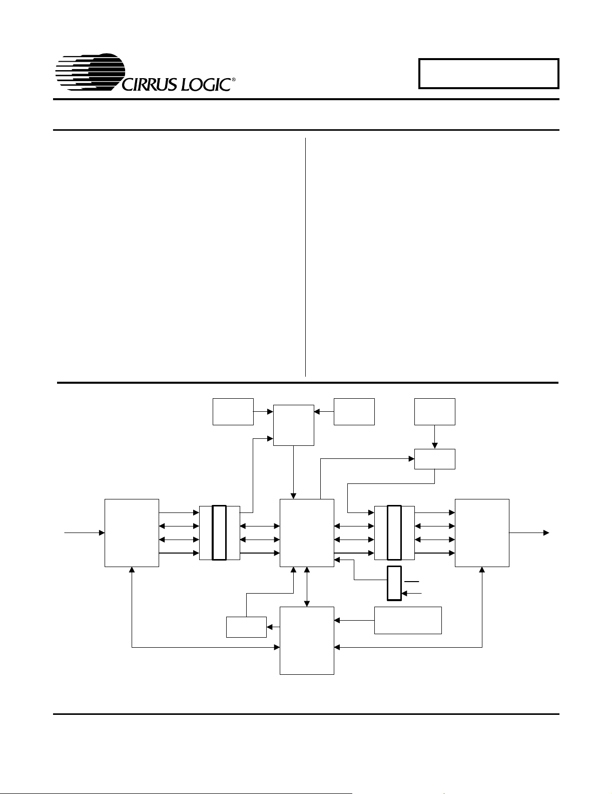
1. SYSTEM OVERVIEW
The CDB8421 demonstration board is an excellent means for evaluating the CS8421 stereo
sample rate converter. Digital audio signal interfaces are provided in the form of S/PDIF receiver
and transmitter and PCM clock/data headers.
The CDB8421 schematic set is shown in Figures 1 through 9 and the board layout is shown in
Figures 10 through 12, and the bill of materials is shown in Table 3.
1.1 CS8421 Sample Rate Converter
A complete description of the CS8421 is included in the CS8421 product data sheet [1], available online at http://www.cirrus.com
D9 (SRC_UNLOCK) indicates when the SRC is not locked and output from the CS8421 SDOUT pin is not valid.
1.2 CS8406 Digital Audio Transmitter
The operation of the CS8406 transmitter and a discussion of the digital audio interface are
included in the CS8406 data sheet [2].
The CS8406 converts the PCM data generated by the CS8421 to the standard S/PDIF data
format. The CS8406 can operate in master or slave mode and accepts 128*Fs, 256*Fs, or
512*Fs master clock on the OMCK input pin. The serial audio input data for the CS8406 is
received from the serial audio output of the CS8421. Digital Interface format selection of I²S
(up to 24-bit), Left Justified (up to 24-bit), or Right Justified (16 or 24-bit) can be made.
S/PDIF output is through J6 or J15.
1.3 CS8416 Digital Audio Receiver
The operation of the CS8416 receiver (see Figure 3) and a discussion of the digital audio interface are included in the CS8416 data sheet [3].
The CS8416 converts the input S/PDIF data stream into PCM data for the CS8421. The
CS8416 operates in master or slave mode and can output either 128*Fs or 256*Fs from its
RMCK pin. Digital Interface format selection of I²S (24-bit), Left Justified (24-bit), or Right
Justified (16 or 24-bit) can be made.
The CS8416 contains an internal input multiplexer which must be set to receive data from
either the optical input connector (J12) or coaxial input connector (J5). This is done by setting
the appropriate switch on switch-bank S4 to the COAXIAL or OPTICAL position.
D10 (RERR) indicates a receiver error, such as loss of lock.
S/PDIF input is through J5 or J12.
DS641DB3 3
Page 4
CDB8421
1.4 Clocking
Table 1 shows the available I/O configurations and their respective clock sources. When the
CS8416 is selected to master SCLK and LRCK (CS8421 input port set to slave), J7 should
be set to 8416. When the CS8421 input port is selected to master SCLK and LRCK (CS8416
set to slave), J7 may be set to 8416, OSC, or XTAL. When the CS8406 is selected to master
SCLK and LRCK (CS8421 output port set to slave), J13 should be set to OSC. When the
CS8421 output port is selected to master SCLK and LRCK (CS8406 set to slave), J13 should
be set to 8421. The board is shipped with a 24.576 MHz crystal/oscillator stuffed at Y1, Y2,
and Y3.
CS8421 Input Port CS8421 Output Port CS8421 XTI/XTO Clock Source CS8406 OMCK Clock Source
Master Slave CS8416 RMCK Y3
Slave Master CS8416 RMCK, Y1, or Y2 CS8421 MCLK_OUT
Slave Slave CS8416 RMCK, Y1, or Y2 Y3
Table 1. Clock Sources
1.5 Clock and Data Headers
The CDB8421 includes headers for input (J8) and output (J11) port clocks and data. These
headers can enabled/disabled using S4. When not using these headers, SDIN should be
jumpered to SDOUT on both J8 and J11. The pin functions for headers J8 and J11 are shown
in Table 7.
The CDB8421 also includes a header for TDM operation (J16). Refer to the CS8421 data
sheet for possible TDM configurations [1]. This header can enabled/disabled using J14.
All headers operate at the VL supply, therefore any external circuit connected to these headers should also operate at VL.
1.6 CPLD Board Setup
The CPLD (U2) controls all of the configuration for the CS8421, CS8416, and CS8406. The
CPLD decodes switches S1, S2, S3, and S4 and sets the appropriate mode of operation.
Switch S1 controls the master/slave and MCLK/LRCK ratio settings for the CS8421, CS8416,
and CS8406. The functions for S1[3:0] are detailed in Table 2.
S1[3:0] CS8421 Input CS8421 Output
0000 Slave Slave
0001 Slave Master (Master Clock = 128*Fs)
0010 Slave Master (Master Clock = 256*Fs)
0011 Slave Master (Master Clock = 384*Fs)
0100 Slave Master (Master Clock = 512*Fs)
1000 Master (Master Clock = 128*Fs) Slave
1001 Master (Master Clock = 256*Fs) Slave
1010 Master (Master Clock = 384*Fs) Slave
1011 Master (Master Clock = 512*Fs) Slave
Table 2. Switch S1, Serial Input and Output Master/Slave and Speed Mode Settings
4 DS641DB3
Page 5
CDB8421
Switch S2 controls the interface format of the CS8406 and the CS8421 output port. The functions for switches S2[3:0] are detailed in Table 3.
S2[3:0] CS8421 Output Configuration
0000 I²S 16-bit Data
0001 I²S 20-bit Data
0010 I²S 24-bit Data
0011 I²S 32-bit Data
0100 Left Justified 16-bit Data
0101 Left Justified 20-bit Data
0110 Left Justified 24-bit Data
0111 Left Justified 32-bit Data
1000 Right Justified 16-bit Data
1001 Right Justified 20-bit Data
1010 Right Justified 24-bit Data
1011 Right Justified 32-bit Data
1100 TDM Mode, 16-bit Data
1101 TDM Mode, 20-bit Data
1110 TDM Mode, 24-bit Data
1111 TDM Mode, 32-bit Data
Table 3. Switch S2, Serial Output Formats
Switch S3 controls the interface format of the CS8416 and the CS8421 input port. The functions for switches S3[2:0] are detailed in Table 4.
S3[2:0] CS8421 Output Configuration
000 I²S up to 32-bit Data
001 Left Justified up to 32-bit Data
010 Right Justified 16-bit Data
011 Right Justified 20-bit Data
100 Right Justified 24-bit Data
101 Right Justified 32-bit Data
110 Left Justified 24-bit Data
Table 4. Switch S3, Serial Input Formats
DS641DB3 5
Page 6

CDB8421
Switch S4 allows any of the PCM clocks/data to be turned off, selection between the OPTICAL and COAXIAL S/PDIF inputs, bypassing the CS8421 sample rate converter, and turning
off the CS8421 MCLK_OUT signal. To input and output S/PDIF to and from the CS8421, the
switches labeled 8416_PCM, 8421_INPUT_PCM, 8421_OUTPUT_PCM, and 8406_PCM
should all be set in the CLOSED position. The functions for switches S4[6:0] are detailed in
Table 5.
Switch Name OPEN CLOSED
8416_PCM Inhibits Clock I/O and Data Output from
CS8416 to Header J8
8421_INPUT_PCM Inhibits Clock I/O and Data Input from
Header J8 to CS8421
8421_OUPUT_PCM Inhibits Clock I/O and Data Output from
CS8421 to Header J11
8406_PCM Inhibits Clock I/O and Data Output from
Header J11 to CS8406
8416_RXSEL Selects Coaxial Connector (J5) for S/PDIF
Input
8421_BYPASS Selects CS8421 SRC Bypass Mode (no
sample rate conversion)
8421_MCLK_OUT CS8421 MCLK_OUT Pin Held Low CS8421 MCLK_OUT Pin Active
Allows Clock I/O and Data Output from
CS8416 to Header J8
Allows Clock I/O and Data Input from
Header J8 to CS8421
Allows Clock I/O and Data Output from
CS8421 to Header J11
Allows Clock I/O and Data Output from
Header J11 to CS8406
Selects Optical Receiver (J12) for S/PDIF
Input
Selects CS8421 SRC Active Mode
Table 5. Switch S4, Board Setup
NOTE:The reset button must be pressed before a new mode of operation takes affect.
Some speed modes and switch combinations are not compatible with the CS8416, CS8421,
or the CS8406. LED’s D4, D5, and D7 indicate that a switch setting is not compatible with the
corresponding part.
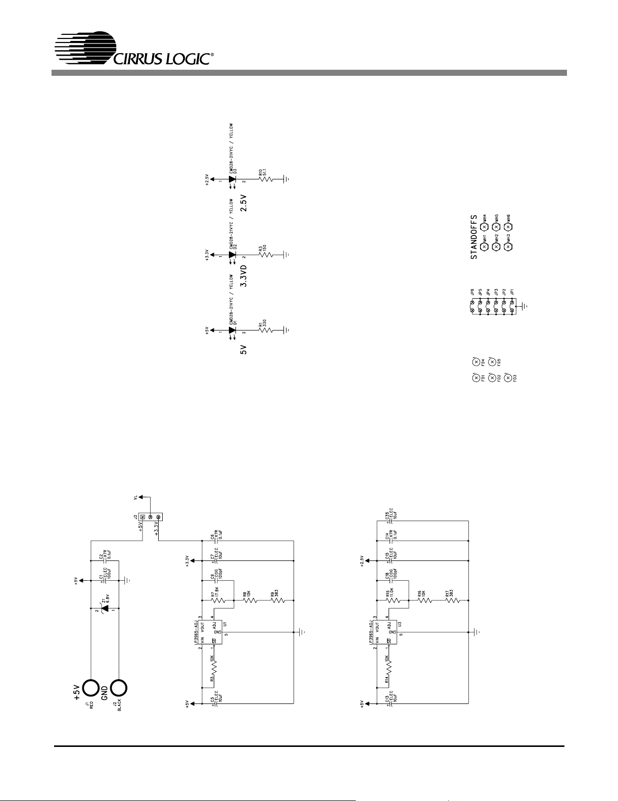
1.7 Power
Power must be supplied to the evaluation board through the +5.0 V binding post (J1). Onboard regulators supply +3.3 V and +2.5 V to the rest of the board. Jumper J3 sets the VL
supply of the CS8416, CS8421, and CS8406 to either +3.3 V or +5.0 V. All voltage inputs
must be referenced to the single black banana-type ground connector (J2).
WARNING:Please refer to the CS8421 data sheet for allowable voltage levels.
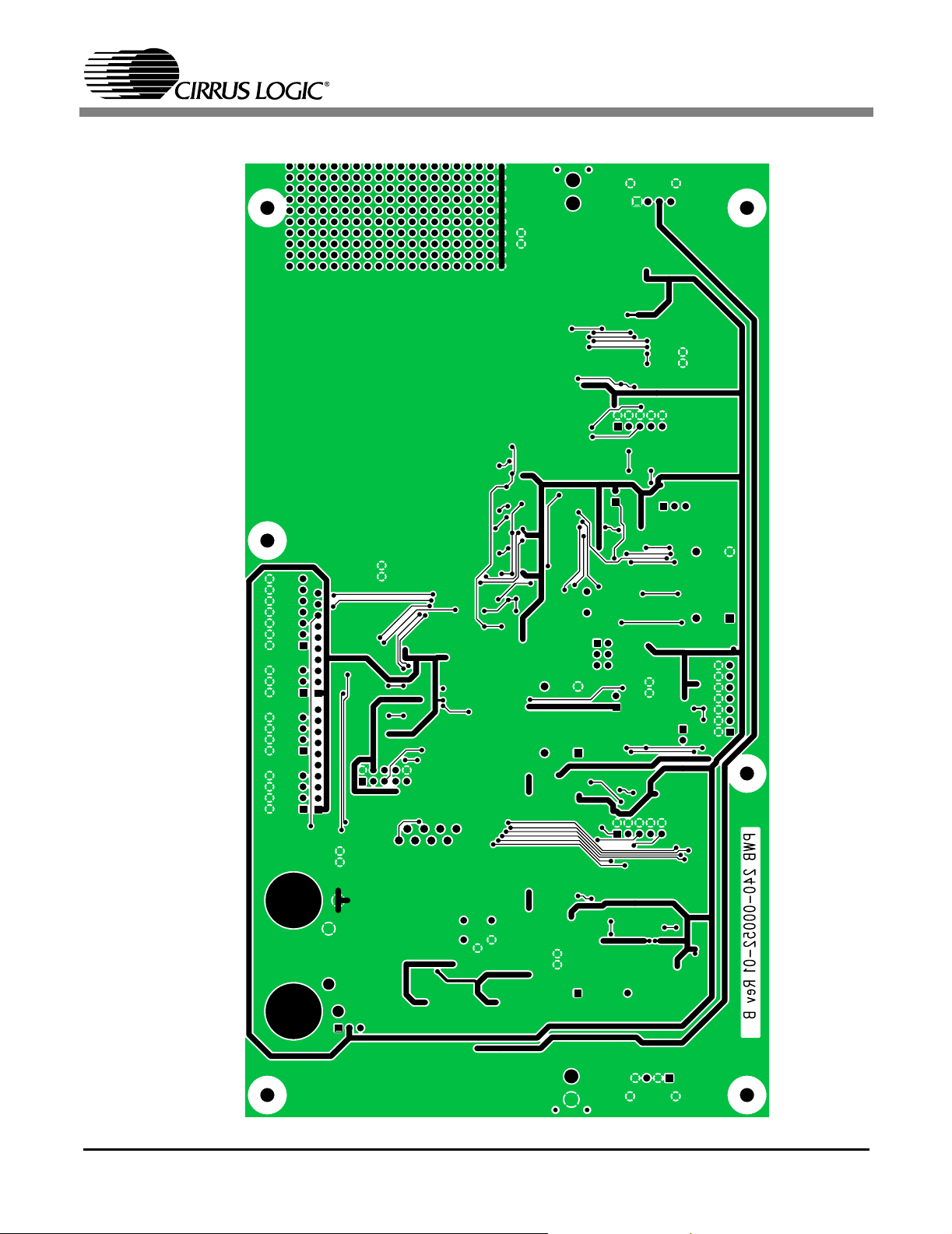
1.8 Grounding and Power Supply Decoupling
The CS8421 requires careful attention to power supply and grounding arrangements to optimize performance. Figure 1 provides an overview of the connections to the CS8421,
Figure 10 shows the component placement, Figure 11 shows the top layout, and Figure 12
shows the bottom layout. The decoupling capacitors are located as close to the CS8421 as
possible. Extensive use of ground plane fill in the evaluation board yields large reductions in
radiated noise.
6 DS641DB3
Page 7
Reference
CONNECTOR
+5V J1 Input +5.0 V Power Supply
GND J2 Input Ground Reference
VL J3 Input +3.3 V to +5.0 V Variable Power Supply for VD
COAX IN J5 Input CS8416 digital audio input via coaxial cable
OPTICAL IN J12 Input CS8416 digital audio input via optical cable
COAX OUT J6 Output CS8406 digital audio output via coaxial cable
OPTICAL OUT J15 Output CS8406 digital audio output via optical cable
PCM Headers J8
TDM Header J16 Input/Output I/O for TDM Clocks & Data
Designator INPUT/OUTPUT SIGNAL PRESENT
Input/Output I/O for PCM Clocks & Data
J11
Table 6. System Connections
PIN SIGNAL
1 Master Clock
2 Serial Bit Clock
3 Left-Right (Word) Clock
4 Serial Data (In for J8, Out for J11)
5 Serial Data (Out for J8, In for J11)
6-10 Ground
CDB8421
Table 7. Header Connections (J8 and J11)
DS641DB3 7
Page 8

2. BLOCK DIAGRAM
CDB8421
Figure 1. Block Diagram
8 DS641DB3
Page 9
3. SCHEMATICS
CDB8421
Figure 2. Power
DS641DB3 9
Page 10

CDB8421
Figure 3. CS8416
10 DS641DB3
Page 11

CDB8421
Figure 4. CS8416 to CS8421
DS641DB3 11
Page 12

CDB8421
Figure 5. CS8421
12 DS641DB3
Page 13

CDB8421
Figure 6. CS8421 to CS8406
DS641DB3 13
Page 14

CDB8421
Figure 7. CS8406
14 DS641DB3
Page 15

CDB8421
Figure 8. Mode Switches
DS641DB3 15
Page 16

CDB8421
Figure 9. CPLD
16 DS641DB3
Page 17

4. LAYOUT
CDB8421
Figure 10. Silk Screen
DS641DB3 17
Page 18

CDB8421
Figure 11. Topside Layer
18 DS641DB3
Page 19
CDB8421
Figure 12. Bottomside Layer
DS641DB3 19
Page 20

CDB8421
5. APPENDIX A: CS8406 TCBL CONNECTION FOR THE CDB8421 REV. A
Pin 15 of U19 on the CDB8421 Rev. A has been lifted. This eliminates the connection to the
TCBL pin on the CS8406 part. The pin should remain lifted and no connection to the pin should
be reestablished for the board to operate properly. Changes have been made to CDB8421
Rev. B boards so that the pin need not be lifted.
20 DS641DB3
Page 21

CDB8421
6. REFERENCES
[1] CS8421 - 32-bit, 192 kHz, Asynchronous, Stereo Sample Rate Converter web page:
http://www.cirrus.com/en/products/pro/detail/P1082.html
[2] CS8406 - 192 kHz Digital Audio Transmitter web page:
http://www.cirrus.com/en/products/pro/detail/P1009.html
[3] CS8416 - 192 kHz Digital Audio Receiver web page:
http://www.cirrus.com/en/products/pro/detail/P1005.html
DS641DB3 21
Page 22
7. REVISION HISTORY
A
A
A
Release Date Changes
DB1 October 2004 1st Release
DB2 November 2004 Corrected figure caption on page 10.
DB3 November 2004 2nd Release
-Updated “Schematics” on page 9 and “Layout” on page 17.
-Updated “References” on page 21.
Table 8. Revision History
CDB8421
Contacting Cirrus Logic Support
For all product questions and inquiries contact a Cirrus Logic Sales Representative.
To find the one nearest to you go to www.cirrus.com
IMPORTANT NOTICE
Cirrus Logic, Inc. and its subsidiaries ("Cirrus") believe that the information contained in this document is accurate and reliable.
However, the information is subject to change without notice and is provided "AS IS" without warranty of any kind (express or
implied). Customers are advised to obtain the latest version of relevant information to verify, before placing orders, that
information being relied on is current and complete. All products are sold subject to the terms and conditions of sale supplied at
the time of order acknowledgment, including those pertaining to warranty, patent infringement, and limitation of liability. No
responsibility is assumed by Cirrus for the use of this information, including use of this information as the basis for manufacture or
sale of any items, or for infringement of patents or other rights of third parties. This document is the property of Cirrus and by
furnishing this information, Cirrus grants no license, express or implied under any patents, mask work rights, copyrights,
trademarks, trade secrets or other intellectual property rights. Cirrus owns the copyrights associated with the information
contained he rein and gives consent for copies to be made of the information on ly for use within your organization with respect to
Cirrus integrated circuits or other products of Cirrus. This consent does not extend to other copying such as copying for general
distribution, advertising or promotional purposes , or for creating any work for resale.
CERTAIN APPLICATIONS USING SEMICONDUCTOR PRODUCTS MAY INVOLVE POTENTIAL RISKS OF DEATH,
PERSONAL INJURY, OR SEVERE PROPERTY OR ENVIRONMENTAL DAMAGE (“CRITICAL APPLICATIONS”). CIRRUS
PRODUCTS ARE NOT DESIGNED, AUTHORIZED OR WARRANTED FOR USE IN AIRCRAFT SYSTEMS, MILITARY
PPLICATIONS, PRODUCTS SURGICALLY IMPLANTED INTO THE BODY, LIFE SUPPORT PRODUCTS OR OTHER
CRITICAL APPLICATIONS (INCLUDING MEDICAL DEVICES, AIRCRAFT SYSTEMS OR COMPONENTS AND PERSONAL OR
UTOMOTIVE SAFETY OR SECURITY DEVICES). INCLUSION OF CIRRUS PRODUCTS IN SUCH APPLICATIONS IS
UNDERSTOOD TO BE FULLY AT THE CUSTOMER’S RISK AND CIRRUS DISCLAIMS AND MAKES NO WARRANTY,
EXPRESS, STATUTORY OR IMPLIED, INCLUDING THE IMPLIED WARRANTIES OF MERCHANTABILITY AND FITNESS FOR
PARTICULAR PURPOSE, WITH REGARD TO ANY CIRRUS PRODUCT THAT IS USED IN SUCH A MANNER. IF THE
CUSTOMER OR CUSTOMER’S CUSTOMER USES OR PERMITS THE USE OF CIRRUS PRODUCTS IN CRITICAL
PPLICATIONS, CUSTOMER AGREES, BY SUCH USE, TO FULLY INDEMNIFY CIRRUS, ITS OFFICERS, DIRECTORS,
EMPLOYEES, DISTRIBUTORS AND OTHER AGENTS FROM ANY AND ALL LIABILITY, INCLUDING ATTORNEYS’ FEES AND
COSTS, THAT MAY RESULT FROM OR ARISE IN CONNECTION WITH THESE USES.
Cirrus Logic, Cirrus, and the Cirrus Logic logo designs are trademarks of Cirrus Logic, Inc. All other brand and product names in
this document may be trademarks or service marks of their respective owners.
22 DS641DB3
 Loading...