

Page 1
Evaluation Board for CS8420
CDB8420
Features
Asynchronous Sample Rate Conversion
Input to output conversion ratio as large as
1:3 or 3:1
Receives and transmits AES/EBU, S/PDIF
and EIAJ-340 compatible digital audio
Runs from a single 5 Volt supply.
Crystals are supplied to allow operation at
44.1 kHz, 48 kHz, and 96 kHz output sample
rates.
Digital patch area.
I
Description
The CDB8420 is de signed to allow rapid evaluation of
the CS8420. Because of the high performance of the
CS8420, the board is set up for e asy connection to an
Audio Precision or a Rohde and Schwarz test system.
Currently available A/D and D/A converters are not adequate to test the full performance of the device.
Input and output data may independently be set to either
AES/EBU or S/PDIF in optical or coaxial physical
formats.
Windows 98 PC software provides a GUI interface to
make configuration easy. The software communicates
through the PC’s RS232 port to a micro-controller on the
evaluation board that controls the CS8420. All the possible software modes of the CS8420 may be tested.
ORDERING INFORMATION
CDB8420 Evaluation Board
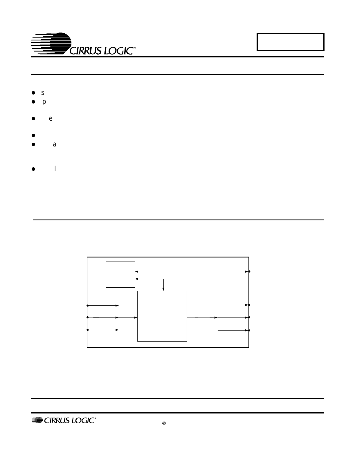
Amtel
µC
Optical In
S/PDIF In
AES 3 In
Preliminary Product Information
http://www.cirrus.com
RS232 port to PC
Optical Out
CS8420
S/PDIF Out
AES 3 Out
This document contains information for a new product.
Cirrus Logic reserves the right to modify this product without notice.
Copyright Cirrus Logic, Inc. 2003
(All Rights Reserved)
Dec ‘03
DS245DB4
1
Page 2

TABLE OF CONTENTS
1. OVERVIEW ...............................................................................................................................3
1.1 CS8420 ............... .......... ................ .......... ......... ................. ......... .......... ................ ..............3
1.2 Micro-Controller and Memory ............................................................................................3
1.3 Crystal Oscil lators ......... ................................. .......... ......... ......... ................. ......... .............. 3
1.4 RS232 Port ......... .......... ................................. .......... ......... ................. ......... .......................3
1.5 LED Function Ind icators ..... ......... ................................. .......... ......... ................. ......... .........3
2. CDB8420.EXE QUICK START GUIDE ....................................................................................5
2.1 Setting up th e hard wa r e : ............... ................. .......... ......... ................. ......... .......................5
2.2 Installing the software: ....................................................................................................... 5
2.3 Starti ng u p the s of twar e : .................... ................. ......... .......... ................................. ...........5
2.4 Starti ng u p the Hardwa r e : ..................... ......... ................................. .......... ......... .......... ......5
3. CDB8420.EXE USER'S GUIDE ................................................................................................6
3.1 Main Window ........................................................................... ....... ....... ....... ..... ....... .........6
3.2 Board Setup .................... .......... ................ .......... ......... ................. ......... ............................7
3.3 Script fi l e synt ax .......................... .......... ......... ................. ......... .......... ....................... .........7
LIST OF FIGURES
Figure 1. CDB8420 Control Panel Main Window ............................................................................6
Figure 2. Board Setup Panel................................................................... .......... ......... ....... .............. 7
Figure 3. CS8420 Sample Rate Converter......................................................................................8
Figure 4. Atmel AVR RISC Micro-controller....................................................................................9
Figure 5. Power Supplies and Reset Circuit..................................................................................10
Figure 6. Silkscreen............... ................. ......... .......... ................................. ......... .......... ................11
Figure 7. Top PCB.........................................................................................................................12
Figure 8. Botto m PCB.................. ................................. .......... ......... ................. ......... .......... .........13
CDB8420
LIST OF TABLES
Table 1. System Connec tions ............. ................. ......... .......... ................ .......... ......... .....................4
Table 2. CDB8420 Jumper Settings................................................................................................4
Table 3. Script file syntax description..............................................................................................7
2 DS245DB4
Page 3

1. OVERVIEW
CDB8420
The CDB8420 evaluation board contains a CS8420
and the supporting circuitry necessary for it to operate. The input and output options include AES3
and S/PDIF in optical and coaxial formats. In software mode, the control registers of the CS8420 are
set by an Atmel AVR RISC micro-controller. A
Windows 98 based program communicates with
the micro through an RS232 port t o control the configuration.
1.1 CS8420
The features and functions of the CS8420 are described in its data sheet.
1.2 Micro-Controller and Memory
The functions of the board are controlled by an Atmel AVR RISC micro-controller. The board is
equipped with 512 kilobytes of static RAM so that
Channel Status and User bits from the AES stream
may be captured and uploaded to the host PC. The
micro-controller communicates with the CS8420
through its SPI port . T he Atmel AVR RISC microcontroller may be bypassed in order to utilize an
external micro-controller through header J10. Additional software development tools and applications information for the Atmel micro-controller
are available at http://www.atmel.com.
1.3 Crystal Oscillators
placed. The oscillator labeled U10 provides the 6
MHz clock for the micro-controller and should not
be changed.
U3 is the oscillator that provides the Output M aster
Clock for the CS8420. The board is shipped with a
12.288 MHz crystal oscillator stuffed at U3 which
sets the output sampling rate to 48 kHz.
Oscillators are also provided for the frequencies of
11.2896 and 24.576 MHz. These allow the SRC to
be operated at output sampling frequencies of 44.1
and 96 kHz.
1.4 RS232 Port
The RS232 port on the upper right hand side of the
board should be connected to the serial port of the
PC running the CDB8420 control software. Follow
the software instructions to properly configure the
serial port for use with the evaluation board.
1.5 LED Function Indicators
LEDs D8 and D9 on the upper right hand corner of
the board allow the user to determine when data is
being transmitted over the RS232 link. The red
LED D4 is the reset indicator and the red LED D1
is connected to the RERR pin of the CS8420. The
two remaining LEDs on the board are not currently
of use to the end user.
There are two crystal oscillators on the board, both
are mounted in pin sockets that allow them to be re-
DS245DB4 3
Page 4
CDB8420
CONNECTOR INPUT/OUTPUT SIGNAL PRESENT
+5V Input +5 Volt power
GND Input Ground connection from power supply
OPTICAL INPUT Input Digital Audio Interface optical input
S/PDIF INPUT Input Digital Audio Interface coaxial input
AES3 INPUT Input Digital Audio Interface XLR input
RS232 Input/Output Parallel RS232 port for connection to serial port of PC
OPTICAL OUTPUT Output Digital Audio Interface optical output (always active)
S/PDIF OUTPUT Output Digital Audio Interface coaxial output
AES3 OUTPUT Output Digital Audio Interface XLR output
J5 Input/Output I/O for RMCLK, ISCLK,ILRCK, and SDIN
J6 Input/Output I/O for OLRCK, OSCLK, OMCK, and SDOUT
J9 Input 10-pin header for external programming of Atmel AVR µC
J10 Input/Output 12-pin header for CS8420 control by external µC
Table 1. System Connections
JUMPER PURPOSE POSITION FUNCTION SELECTED
J11 Selects physical format of digital
audio interface input
J12 Enables AES3 INPUT ENABLE
J13 Enables S/PDIF INPUT ENABLE
J14 Enables OPTICAL INPUT ENABLE
J16 Selects physical format of digital
audio interface output
J17 Enables S/PDFIF OUTPUT ENABLE
J15 Enables HARDWARE MODE MUTE ENABLE
Table 2. CDB8420 Jumper Settings
AES3 & S/PDIF
OPTICAL
DISABLE
DISABLE
DISABLE
AES3
S/PDIF
DISABLE
DISABLE
Specifies input as either AES3 or S/PDIF type
Specifies input as OPTICAL type
AES3 INPUT enabled
AES3 INPUT disabled
S/PDIF INPUT enabled
S/PDIF INPUT disabled
OPTICAL INPUT enabled
OPTICAL INPUT disabled
Specifies output as AES3 XLR
Specifies output as coaxial S/PDIF
S/PDIF OUTPUT enabled
S/PDIF OUTPUT disabled
Enables MUTE when in hardware mode 1
Disables MUTE when in hardware mode 1
4 DS245DB4
Page 5

CDB8420
2. CDB8420.EXE QUICK START GUIDE
2.1 Setting up the hardware:
1) Connect the CDB8420 to a 5V DC power supply.
2) Set: J11 to Optical, J16 to S/PDIF, enable J13
(S/PDIF), and disable J15 (MUTE).
3) Connect the CDB8420 to the PC COM port using RS232 cable.
4) Apply power to the board.
5) Press the RESET switch (S5).
At this point, the RERR and PROC should be lit.
The hardware is now ready!
2.2 Installing the software:
1) Create a directory called CDB8420 anywhere
on your system.
2) Copy CDB8420.exe into this directory.
3) If you do not already have them, copy the included DLLs msvcrt.dll and mfc42.dll into
your \Windows\System directory.
4) If desired, create a sho rtcut to CDB8420.exe on
your desktop.
At this point, you are ready to start up the software.
2.3 Starting up the software:
1) Double-click on CDB8420.exe or its shortcut.
2) If you get errors right away, the COM port
needs to be set properly.
3) Click anywhere but inside one of the boxes, this
brings up the Board Setup control panel.
4) Select the COM port you are using to connect
to the CDB8420.
5) Shut down the application, reset the board, and
then restart the application.
2.4 Starting up the Hardware:
1) Click anywhere but inside one of the boxes, this
brings up the Board Setup control panel.
2) Click on the Reset button. You should see the
TX and RX leds light up briefly.
3) Click on the Sample Rate Converter tab, then
set the SRC data source to AES3 Receiver.
4) Click on the Clock Sources tab, uncheck the
Stop Internal Clocks box and click on RMCK
derived from AES3 input frame.
5) Check the performance of the board by doing
an FFT with a -1dBFS 1kHz sine w ave for input at 44.1kHz and 48kHz sample rates using
the optical input and optical output.
DS245DB4 5
Page 6

CDB8420
3. CDB8420.EXE USER'S GUIDE
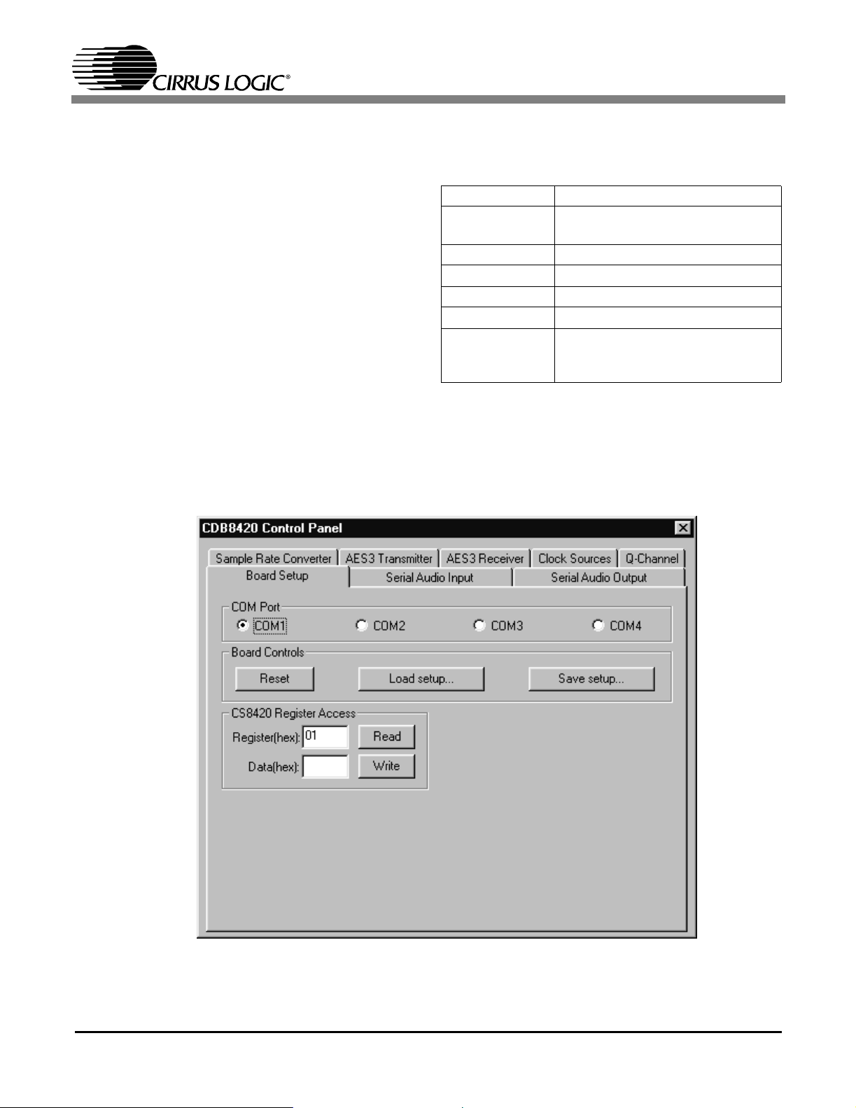
3.1 Main Window
The CDB8420 Control Panel allows you to view
and access the data flow configuration of the
CS8420. Clicking the right mouse button in any of
the boxes will bring up a property menu containing
all the register bits relevant to that block, as well as
some high level functions, such as data sources and
formatting options.
To access additional details about each block, click
the left mouse button on the desired block. This
will display a control panel for the selected block.
If you click outside the boxes, you will bring up the
Board Setup control panel, as shown on the next
page. Note that you can click on any of the tabs to
quickly access that section. Also, any changes you
make in the panel are immediately reflected in the
Main Window, so you may wish to arrange them so
that they do not obscure each other.
Figure 1. CDB8420 Control Pane l Main Window
6 DS245DB4
Page 7
CDB8420
3.2 Board Setup
The Board Setup panel has some very useful functions, including setting the COM Port used by the
application, resetting the CS8420 by the software,
as well as loading/saving register settings into files .
You can also can read or wr ite any register on the
CS8420 using the CS8420 Register Access.
3.3 Script file syntax
The setup files generated by the board setup function only record the state of the chip registers.
There are many more useful commands that you
can insert into the setup s c ripts . Here is a shor t description of them with their allowed syntax.
NOTE: Most commands accept either hexadecimal
(indicated by either a "0x" prefix or "h" suffix) or
decimal parameters.
// used for single line comments
script scriptfile call an external script file named
"scriptfile"
reset 1 assert reset of the CS8420
reset 0 de-assert re se t of th e CS8420
wr 1 30h write register 1 with hex 30
set DITH 1 set the bit field labeled DITH to 1
write 2 3 0x10
12h 13
Table 3. Script file syntax description
write 3 consecutive registers start-
ing from register 2 with hex 10, hex
12, and decimal 13
Figure 2. Board Setup Panel
DS245DB4 7
Page 8

CDB8420
APMS S/AES
123
R14 6.2K
R13
R12
R11
R10
R9
5
OPT2
4
C3
.1uF
47K
47K
47K
47K
47K
CCLKCDOUT
PHONO-JACK
TRANSFORMER
R16 110
C5
.1uF
TP25
TP26
TP27
TP28
CDIN
CCLK
J2
TP24
TXP
123
TP23
TXN
6 2
1 8
4 5
J16
HDR3X1
R18
681
R19
84.5
TP15
TP16
TP17
TP18
TP19
TP20
TP21
TP22
OSCLK
OLRCK
OMCK
SDOUT
16181719202122232425262728
U
VD
INT
H/S
GND
OMCK
OSCLK
OLRCK
SDOUT
T2
123
J17
R21
78
56
132
1000pF
HDR3X1
22K1
J6
3
C41
HDR4X2
4
C8
22pF
1
2
J4
XLR-MALE
D
of
13Wednesday, November 12, 2003
Semiconductor Products Division
VD
L2 FERRITE BEAD
R24 2 Ohms
C15
1uF 50V
+
.1uF
OMCK
OSCLK
OLRCK
SDOUT
C14
C11
.1uF
C17
1
1000pF
C16
NC
VD
U3
14
R26
VD
+
1uF 50V
SCHM DWG CDB8420 (600-00100-01)
Gomez Marketing Evaluation Board
B
Title
Size Document Number Rev
Date: Sheet
78
GNDOut
12.888MHz
100
6
VD
INT
SUP4
CEN
H/S
CDIN/CS
SFMT1
/RST
SFMT0
SUP2
SUP1SUP3
TCBLD
C1 .01uF
SUP0 SUP5
MUTE
123
6
C9
1000pF
78
56
132
R20
C6
J12
R22
J5
4.7K
.1uF
HDR3X1
123
1.6K
C7
4700pF
.1uF
HDR4X2
4
VD
123
C40
HDR3X1
C12
0.33uF
+
VA
+
C13
1uF 50V
C10
D1
LED_R
2 1
R25
RMCK
ISCLK
ILRCK
SDIN
HDR3X1
J15
22pF
2
XLR-FEMALE
3
825
74VHC125
2 3
1
A B C D E
U2A
J3
1
Figure 3. CS8420 Sample Rate Converter
CDOUT
/CS
/EMPH
RXP
RXNVAAGND
FILT
/RST
RMCK
RERR
ILRCK
ISCLK
TP9
6 2
1011121314 15
RMCK
TP10
TP11
TP12
TP13
HDR3X1
J14
J13
ILRCK
TP14
123
123
ISCLK
SDIN TCBL
SDIN
U1 CS8420
123
.1uF
J1
TP1
J11
HDR3X1
TRANSFORMER
PHONO-JACK
123456789
TP2
TP3
TP4
TP5
TP6
TP7
TP8
R17
110
R15
236
T1
1 8
4 5
C4
.1uF
R8
47K
R7
47K
R6
47K
R5
47K
R4
47K
R3
47K
R2
47K
R1
47K
L1
47UH
VD
C2
4
OPT1
5
8 DS245DB4
Page 9

P1
594837261
D7 1N4148
CONNECTOR DB9
D6 1N4148
12
12
21
D9 LED_R
D8 LED_G
21
CDB8420
D
of
R34
680
R33
680
33Wednesday, November 12, 2003
C39
171819202122232425262728293031
PB7
TOSC2
AGND
AVCC
64
.1uF
C38
.1uF
C37
.1uF
VD
C36
.1uF
C35
.1uF
C32
+
C34
.1uF
C33
1000pF
1
78
NC
GNDOut
U10
6.000MHz
VD
14
R35 100
TP29
TP31
PB6
16
PB5
15
PB4
14
PB3/CDOUT
13
PB2/CDIN
12
PB1/CCLK
11
PB0/CS
10
PE7
9
PE6
8
PE5
7
PE4
6
PE3
5
PE2
4
PE1/TXD
3
PE0/RXD
2
/PEN
1
TP30
VD
VD
21
D10
LED_G
R32 1K
2
6
V-
V+
GNDVD
1516
U9
DS232
T1 IN T1 OUT
R1 IN R1 OUT
C1+
C1-
T2 IN T2 OUT
R2 IN R2 OUT
C2+
D5
LED_G
2 1
R30
825
.1uF
C31
.1uF
C30
.1uF
C29
C28
.1uF
C27
.1uF
VD
C26
.1uF
C25
.1uF
+
C24
1uF 50V
+
C23
1uF 50V
A18
1
A16
A15
31
A17
30
/WE
29
A13
28
A13
A8
27
A8
A9
26
A9
A11
25
A11
/OE
24
A10
23
A10
/CS
22
D7
21
D7
D6
20
D6
D5
19
D5
D4
18
D4
D3
17
D3
Q8
12
Q7
13
Q6
14
Q5
15
Q4
16
Q3
17
Q2
U5 74HC574
18
Q1
19
U6 HM628512
OC
CLK
D8
D7
D6
D5
D4
D3
D2
D1
2
A14
3
A14
A12
4
A12
A7
5
A6
6
A5
7
A4
8
A3
9
A2
10
A1
11
A0
12
D0
13
D0
D1
14
D1
D2
15
D2
1
11
9
D7
8
D6
7
D5
6
D4
5
D3
4
D2
3
D1
2
D0
U2D
OC
C
Q8
D8
12
Q7
D7
13
Q6
D6
14
Q5
D5
15
Q4
D4
16
Q3
D3
17
Q2
D2
U7 74HC573
18
Q1
D1
19
74VHC125
1
11
9
8
7
6
5
4
3
2
13
12 11
33
34
35
A8
36
A9
37
A10
38
A11
39
A12
40
A13
A[8-14]
41
A14
42
43
D[0-7]
44
45
46
47
48
D7
D6
D5
D4
D3
D2
D1
D0
11 14
13 12
10 7
VD
L4
MUTE
SFMT1
CEN
SFMT0
H/S
S/AES
32
PD1
PD2
PD3
PD4
PD5
PD6
PD7
/WR
/RD
PC0
PC1
PC2
PC3
PC4
PC5
PC6
PC7
ALE
U8
PA7(AD7)
PA6(AD6)
PA5(AD5)
PA4(AD4)
PA3(AD3)
PA2(AD2)
PA1(AD1)
PA0(AD0)VDGND
PF7(ADC7)
PF6(ADC6)
495051525354555657585960616263
VD
1
8 9
FERRITE BEAD
XTAL2
XTAL1
PD0/INT0
ATmega103
PF5(ADC5)
PF4(ADC4)
PF3(ADC3)
3
4
R31
VD
MRST
VD
GND
/RST
PF2(ADC2)
PF1(ADC1)
PF0(ADC0)
C2-
5
2 Ohms
TOSC1
AREF
Semiconductor Products Division
Title
1uF 50V
CDIN
/CS
/RESET
CDOUT
CCLK
INT
1
3
5678910
1112
J10
2
4
SUP3
SUP5
TCBLD
SUP4
APMS
C
9
B
10
A
11
INH
6
Z1
Z
Y
X
U11 74HC4053
3
Z0
5
Y1
1
Y0
2
X1
13
X0
12
4
15
14
SCHM DWG CDB8420 (600-00100-01)
CS8420 Marketing Evaluation Board
B
Size Document Number Rev
Date: Sheet
HDR6X2
SUP1
SUP2
SUP0
Figure 4. Atmel AVR RISC Micro-controller
VD
R37 100
J9
HDR5X2
A B C D E
TP32
4
VD
234561789
RN1
8x 47K
/PGM
16151413121110
9
S6
8
SW DIP-8
1234567
R36 100
132
56
78
910
DS245DB4 9
Page 10

CDB8420
D
VA
VD
/RESET
D2
R28
BAT85
U2B
/RST
74VHC125
5 6
47K
1 2
4
BAT85
D3
12
VD
D4
21
VD
/PGM
LED_R
R29
U2C
825
74VHC125
9 8
of
23Wednesday, November 12, 2003
10
Semiconductor Products Division
SCHM DWG CDB8420 (600-00100-01)
Gomez Marketing Evaluation Board
A
Title
Size Document Number Rev
Date: Sheet
C19
C18
+
R27
.1uF
100uF 6.3V
2 Ohms
L3
FERRITE BEAD
D11
BAT85
1 2
C21
.1uF
C20
100uF 6.3V
+
Z1
P6KE6.8A
1 2
RED
1
J8
1
J7
VD
BLACK
R38
10K
MRST
C22
.01uF
Figure 5. Power Supplies and Reset Circuit
S5
SW_MOM
1 3
5
A B C D E
10 DS245DB4
Page 11

CDB8420
Figur e 6. Silks c reen
DS245DB4 11
Page 12

CDB8420
Figure 7. Top PCB
12 DS245DB4
Page 13

CDB8420
Figure 8. Bottom PCB
DS245DB4 13
Page 14

Revision History
Release Date Changes
DB4 Nov 12, 2003 Updated schematics.
Moved legal statement to end of document and updated.
Added revision block.
CDB8420
Contacting Cirrus Logic Support
For a complete listing of Direct Sales, Distributor, an d Sales Representative co ntacts, visit the C ir rus Logi c web site at :
http://www.cirrus.com/corporate/contacts
Cirrus Logic, Inc. and its subsidiaries (" Cirrus") believe that the information contained in this docu men t is accur ate and reliab le. H owev er, the information is subject to change
without notice an d i s pr ovided "A S IS " w i t hout warra nty of any kind (e xpress or implied). Customers a re a dvised to ob t ai n t he l atest version of relevant information to verify,
before placing orders, that information being relied on is current and complete. All products are sold subject to the terms and conditions of sale supplied at the time of order
acknowledgment, includin g th ose p ertaining to warr anty , patent infringemen t, a nd limitation of liability. No r espo nsibility is as s umed by C irrus for the use of this informa tio n,
inclu di ng use o f t hi s information as the ba s i s for manu factur e or sale of an y i tems, or for infring em e nt of pate nt s or othe r rights of third parties. This document is the property
of Cirru s an d by fu rn ish ing th is i nfo rma ti on, Cir rus gra nts no li ce nse, ex pr ess or imp li ed un der any pa te nt s, ma sk wo rk ri ght s , copyrights, trademarks, trade secrets or other
intell ec t ual propert y rights. Cirrus ow ns the copyright s associat e d with the infor m at i on cont ai ne d herein a nd gives consent for co pie s t o be m ade of the informati on only for use
withi n your organization with respe c t t o Cirrus int e grated circ ui ts or other products of Cirrus. T his consent does not ext e nd to other copying such as copying for gene ral distributio n, advertising or promoti onal pur poses, or for creating a ny work for resale.
An export permit needs to be obtained f rom the com petent authorities of the Ja panese Gov ernment if any o f the products or techn ologies desc ribed in this material and controlled
under the "Foreign Ex change and Foreign Trad e Law " is to be exported o r taken out of Jap an. An exp ort license and/o r quota needs to be obtained from the comp etent auth orities
of the Chinese Government if any of the products or technologies described in this material is subject to the PRC Foreign Trade Law and is t o be ex po rted or tak en out of th e P RC.
CERTAIN APPLICATIONS USING SEMICONDUCTOR PRODUCTS MAY INVOLVE POTENTIAL RISKS OF DEATH, PERSONAL INJURY, OR SEVERE PROPERTY OR ENVIRONMENTAL DAMAGE (“CRITICAL APPLICATIONS”). CIRRUS PRODUCTS ARE NOT DESIGNED, AUTHORIZED OR WARRANTED FOR USE
IN AIRCRAFT SYSTEMS, MILITARY APPLICATIONS, PRODUCTS SURGICALLY IMPLANTED INTO THE BODY, LIFE SUPPORT PRODUCTS OR OTHER CRITICAL APPLICATIONS (INCLUDING MEDICAL DEVICES, AIRCRAFT SYSTEMS OR COMPONENTS AND PERSONAL OR AUTOMOTIVE SAFETY OR SECURITY DEVICES). INCLUSION OF CIRRUS PRODUCTS IN SUCH APPLI CATIONS IS UNDERSTOOD TO BE FULLY AT THE CUSTOMER’S RISK AND CIRRUS
DISCLAIMS AND MAKES NO WARRANTY, EXPRESS, STATUTORY OR IMPLIED, INCLUDING THE IMPLIED WARRANTIES OF MERCHANTABILITY AND
FITNESS FOR PARTICULAR PURPOSE, WITH REGARD TO ANY CIRRUS PRODUCT THAT IS USED IN SUCH A MANNER. IF THE CUSTOMER OR CUSTOMER’S CUSTOMER USES OR PERMITS THE USE OF CIRRUS PRODUCTS IN CRITICAL APPLICATIONS, CUSTOMER AGREES, BY SUCH USE, TO FULLY INDEMNIFY CIRRUS, ITS OFFICERS, DIRECTORS, EMPLOYEES, DISTRIBUTORS AND OTHER AGENTS FROM ANY AND ALL LIABILITY, INCLUDING
ATTORNEYS’ FEES AND COSTS, THAT MAY RESULT FROM OR ARISE IN CONNECTION WITH THESE USES.
Cirrus L ogic, Cirrus, and th e Ci rrus Log ic logo designs are t ra demarks of Cirrus Logic, Inc . A l l other bran d a nd produ c t names in this document may be trademarks or service
marks of their respective owners.
I2C is a registered trademark of Philips Semiconductor. Purchase of I2C Components of Cirrus Logic, Inc., or one of its sublicen se d Asso ciated Comp anie s conveys a license
under the Philips I2C Patent Rights to use those compo ne nts in a standa rd I2C system.
14 DS245DB4
 Loading...