

Page 1

Evaluation Board for CS8130
CDB8130
Features
z Designed to conform to IrDA Physical Layer
Specification
z Interfaces to PC Serial Port
z Operates from +2.7 V to 5.5 V Power Supply
z Includes Evaluation Software
VA+
AGND DGND
Description
The CDB8130 evaluation board allows fast and easy
evaluation of the CS8130 infrared transceiver. The
board contains an RS-232 level shifter and DB-9 serial
connector to allow easy interfacing to a standard PC serial (COM) port.
Additionally, the board is shipped with a complete set of
diagnostic and test software, as well as the Infrared Data
Association Link Access Protocol (IrLAP) reference
code.
ORDERING INFORMATION
CDB8130
VD+
LEDs
and
PIN
Diode
http://www.cirrus.com
CS8130
RESET
Circuit
RS-232
Level
Translator
Copyright © Cirrus Logic, Inc. 2006
(All Rights Reserved)
9-Pin
Serial
Connector
MAR ‘06
DS170DB5
Page 2

CDB8130
TABLE OF CONTENTS
1 CS8130 INFRARED TRANSCEIVER ........................................................................................ 3
1.1 Power Supply Circuitry and Grounding .. .... ... ... ... .... ... ... ... .... ... ... ... ... .... ... ........................... 3
1.2 Reset Circuit ....................................... ... .... .......................................... ... ... ........................3
1.3 Optical Interface ..... ... .... ... ... ... .... ... .......................................... ... ... ... .... ... ...........................3
1.4 RS-232 Interface ....... .... .......................................... ... ... ... .... ... ........................................... 5
1.5 Header Interface ........................... ... ... ... .... .......................................... ... ........................... 5
1.6 Clock Selection ................................ ... ... .... ... ... .......................................... ... .... ... ... ... ........ 6
1.7 Power Down .......................................................................................................................6
1.8 Status Indicator LEDs ........................................................................................................ 6
1.9 Software .... .......................................... ... .... .......................................... ... ...........................6
2 REVISION HISTORY .............................................................................................................. 10
LIST OF FIGURES
Figure 1. CS8130 and RS-232 Level Translator............................................................................. 4
Figure 2. Power Supply Circuitry..................................................................................................... 5
Figure 3. Reset Circuit.....................................................................................................................5
Figure 5. Unused Gates and Resistors........................................................................................... 7
Figure 4. Power Supply Circuitry..................................................................................................... 7
Figure 6. Component-side Silkscreen (Not to Scale) ...................................................................... 8
Figure 7. Component-side Trace Layer (Not to Scale)....................................................................9
Figure 8. Solder-side Trace Layer (Not to Scale)..........................................................................10
Contacting Cirrus Logic Support
For all product questions and inquiries contact a Cirrus Logic Sales Representative.
To find the one nearest to you go to www.cirrus.com
IMPORTANT NOTICE
Cirrus Logic, Inc. and i t s s ubs idi ar i es (“ Cir rus ” ) be l ie ve t hat th e i nf ormation contained in this doc um ent is ac cu ra te a nd rel iable. However, the information is subject
to change without notice and is provided “AS IS” without warranty of any kind (express or implied). Customers are advised to obtain the latest version of relevant
information to verify, before placing orders, that information being relied on is current and complete. All products are sold subject to the terms and conditions of sale
supplied at the time of order acknowledg ment, including thos e pertaining to warranty, indem nification, and limitatio n of liability. No responsibility is assumed by Cirrus
for the use of this information, including use of this information as the basis for manufacture or sale of any items, or for infringement of patents or other rights of third
parties. This document is the property of Cirrus and by furnishing this information, Cirrus grants no license, express or implied under any patents, mask work rights,
copyrights, trademarks, trade secrets or other intellectual property rights. Cirrus owns the copyrights associated with the information contained herein and gives consent for copies to be made of the information only for use within your organization with respect to Cirrus integrated circuits or other products of Cirrus. This consent
does not extend to other copying such as copying for general distribution, advertising or promotional purposes, or for creating any work for resale.
CERTAIN APPLICATIONS USING SEMICONDUCTOR PRODUCTS MAY INVOLVE POTENTIAL RISKS OF DEATH, PERSONAL IN JURY, OR S EVERE PROPERTY OR ENVIRONMENTAL DAMAGE (“CRITICAL APPLICATIONS”). CIRRUS PRODUCTS ARE NOT DESIGNED, AUTHORIZED OR WARRANTED FOR USE
IN AIRCRAFT SYSTEMS, MILI TARY APPLI CATIONS, PRODUCT S SURGICALL Y IMPLANTED I NTO THE BODY, AUTOMOTIVE SAFET Y OR SECURITY DEVICES, LIFE SUPPORT PRODUCTS OR OTHER CRITICAL APPLICATIONS. INCLUSION OF CIRRUS PRODUCTS IN SUCH APPLICATIONS IS UNDERSTOOD
TO BE FULLY AT THE CUSTOM ER'S R ISK A ND CIRRUS DISCLAIMS AND MAKES NO WARRANTY, EXPRESS, STATUTORY OR IMPLIED, INCLUDING THE
IMPLIED WARRANTIES OF MERCHANTABILITY AND FITNESS FOR PARTICULAR PURPOSE, WITH REGARD TO ANY CIRRUS PRODUCT THAT IS USED
IN SUCH A MANNER. IF THE CUSTOMER OR CUSTOMER'S CUSTOMER USES OR PERMITS THE USE OF CIRRUS PRODUCTS IN CRITICAL APPLICATIONS, CUSTOMER AGREES, BY SUCH USE, TO FULLY INDEMNIFY CIRRUS, ITS OFFICERS, DIRECTORS , EMPLOYEES, DISTRIBUTORS AND OTHER
AGENTS FROM ANY AND ALL LIABILITY, INCL UDING ATTORNEYS' FEES AND COSTS, THAT MAY RESULT FROM OR ARISE IN CONNECTION WITH
THESE USES.
Cirrus Logic, Cirrus, and the Cirrus Logic logo designs are trademarks of Cirrus Logic, Inc. All other brand and product names in this document may be trademar ks
or service marks of their respective owners.
IBM is a registered trademark of International Business Machines Corporation.
Temic is a registered trademark of Temic Telefunken Microelectronics, GmbH.
Hewlett-Packard is a registered trademark of Hewlett-Packard Corporation.
2 DS170DB5
Page 3

CDB8130
1 CS8130 INFRARED TRANSCEIVER
The CDB8130 provides an example application of
the CS8130 infrared transceiver. This application
is similar to an IR pod system that is designed to
plug into any standard RS-232 port, like the COM
port on the back of an IBM®-compatible PC, to
provide an easy-to-use infrared interface.
Additionally, the board allows for easy interfacing
directly to the CS8130 through stake header J11 allowing other applications to be easily realized.
Figure 1 shows the CS8130 and RS-232 level
translator connections.
A description of the CS8130 including register definitions, control pin assignments, and other useful
information can be found in the CS8130 data sheet.
1.1 Power Supply Circuitry and Grounding
Figure 2 shows the power supply configuration of
the evaluation board. Power is supplied to the
board by two terminal blocks and a DC power jack,
J21, J22, and J23 (DCPWR). To operate the board
from a single power supply, stake jumper J20 must
be installed. In this configuration, power should be
supplied to the board through the VD+/DGND terminal block (J21) or the DCPWR jack (J23).
A 3.3V regulator, U5, is supplied on the board. To
use this regulator, stake jumper J2 (USE REG)
should be installed. To bypass the regulator, J1
(NO REG) should be installed.
To isolate the power supply driving the CS8130
from the supply powering the rest of the circuitry,
remove J20, and feed the CS8130’s power supply
into the VA+/AGND terminal block (J22). The rest
of the circuit should be powered through either the
VD+/DGND terminal block (J21) or the DCPWR
jack (J23).
Using the on-board voltage regulator, the evaluation board may be powered from any DC voltage
between +4V and +6.5V. If the voltage regulator is
bypassed, the acceptable operating voltage is be-
tween +2.7V and +5.5V (defined by the power supply requirements of the CS8130.)
The evaluation board is split into two ground
planes, an analog plane and a digital plane. The
CS8130 and IR components reside on the analog
plane, and the RS-232 level translator, reset circuit,
and status indicator circuitry lie over the digital
ground plane. The ground planes are connected in
exactly one place at jumper J31, located near the
power supply connections.
1.2 Reset Circuit
Figure 3 shows the power-up and user-activated reset circuit. As shipped from the factory, this circuit
is not used. The RESET
by the RS-232 interface signal RTS. This configuration allows the CS8130 to be reset under software
control.
To derive the reset function from the powerup/manual reset circuit instead, remove stake
jumper J9 (RTS) and install stake jumper J12 (RESETSW). These jumpers are shown in Figure 1.
signal is instead supplied
1.3 Optical Interface
The CDB8130 is shipped with Temic® and
Hewlett-Packard® IR components installed. The
receiver PIN diode is Temic model BPV 22 NF.
Transmit LED D5 is a Hewlett-Packard HSDL4220, and D6 is a Temic TSHA5502.
These components are not soldered in place. Instead, they are held by gold-plated pins. These pins
allow for any insertion and removal of other IR
components for performance and compatibility
evaluation.
The default configuration for the transmitter circuit
has one LED per output driver. One or both LEDs
can be active at the same time by programming the
appropriate register in the CS8130, allowing software to control the transmitter output power.
Additionally, the transmit drivers on the CS8130
can be connected in parallel to share current. This
DS170DB5 3
Page 4

CDB8130
Figure 1. CS8130 and RS-232 Level Translator
4 DS170DB5
Page 5

CDB8130
Figure 2. Power Supply Circuitry
Figure 3. Reset Circuit
allows systems using only one LED to operate with
a much higher drive current than can be sourced by
using a single driver. To connect the transmitter
drivers in this way, install jumper J17.
The LED transmitter driver resistors (R3 and R4)
are optimized for a power supply voltage of 3.3V.
For operation at voltages greater than this, the values of these resistors must be increased.
1.4 RS-232 Interface
The CDB8130 is designed to connect to any standard RS-232 port through the female DB-9 connector marked “RS-232.” The MAX562 (U2) supplies
the voltage level translation function, taking the ±
12V RS-232 levels and translating them to standard
CMOS logic levels.
Table 1 shows the default mapping of UART signals to CS8130 pins.
CS8130 Pin UART Signal Direction
RXD RXD to UART
TXD TXD to CS8130
FORM/BSY CTS
D/C
RESET
Table 1. CS8130-to-UART Connections
DTR to CS8130
RTS to CS8130
to UART
1.5 Header Interface
If desired, the RS-232 level translator can be removed from the circuit. The signals are disconnected by removing jumpers J5, J6, J7, J8, and J9.
DS170DB5 5
Page 6

CDB8130
Removing J35 will disconnect power from the level translator.
All the digital signals on the CS8130, FORM/BSY,
D/C, TXD, RXD, EXTCLK, RESET, PWRDN,
and CLKFR can be accessed directly from header
J11. All digital input pins are tied to 47 kΩ pull-up
resistors through resistor set R1.
1.6 Clock Selection
The clock for the CS8130 can be supplied via a
crystal tied between XTALIN and XTALOUT (the
default configuration on the evaluation board) or
by an external clock supplied through the EXTCLK pin.
To operate the CS8130 from an external clock
source, cut the trace under J3 (XTAL), and the
(XTAL) part of J4, then connect the center pin of J4
to the edge pin marked EXT.
Note: the EXTCLK pin on the CS8130 can be either an input or an output. If the CS8130 is being
clocked from a crystal, EXTCLK is an output. If
no crystal is present, EXTCLK is an input. This determination of direction is made while RESET is
asserted.
The CS8130 can be operated from either a 3.6864
MHz or a 1.8432 MHz clock source. If operating
from a 3.6864 MHz source, jumper J18 (CLKFR)
must be installed. This brings the CLKFR pin on
the CS8130 low. If operating from a 1.8432 MHz
source, jumper J18 should be removed.
it means when a LED is lit can be confusing. Table
2 should help clarify this.
Name LED On means. . .
LED1C Transmitter #1 active
LED2C Transmitter #2 active
PWRDN
RESET
RXD Data being received by the CS8130
TXD Data being transmitted to the CS8130
D/C
FORM/BSY Auto detect ASK/TV TX ready
Table 2. LED Indicator Meanings
Power down asserted
Reset asserted
CS8130 in Control Mode
1.9 Software
The CDB8130 evaluation kit comes equipped with
software that can be used to evaluate and test the
CS8130. Additional software is currently under
development.
See the documentation supplied with the CDB8130
evaluation kit for instructions on how to use the
software.
Software updates and new releases can be downloaded from the Crystal BBS. Contact the factory
for details.
1.7 Power Down
Jumper J14 (PWRDN) controls the state of the
PWRDN pin on the CS8130. PWRDN is asserted
when J14 is installed.
1.8 Status Indicator LEDs
Key digital signals on the CS8130 are displayed on
indicator LEDs U6 (U8) and U7 (U9), shown schematically in Figure 4. Because these LEDs are
driven through inverters, the interpretation of what
6 DS170DB5
Page 7

CDB8130
Figure 4. Power Supply Circuitry
Figure 5. Unused Gates and Resistors
DS170DB5 7
Page 8

CDB8130
Figure 6. Component-side Silkscreen (Not to Scale)
8 DS170DB5
Page 9

CDB8130
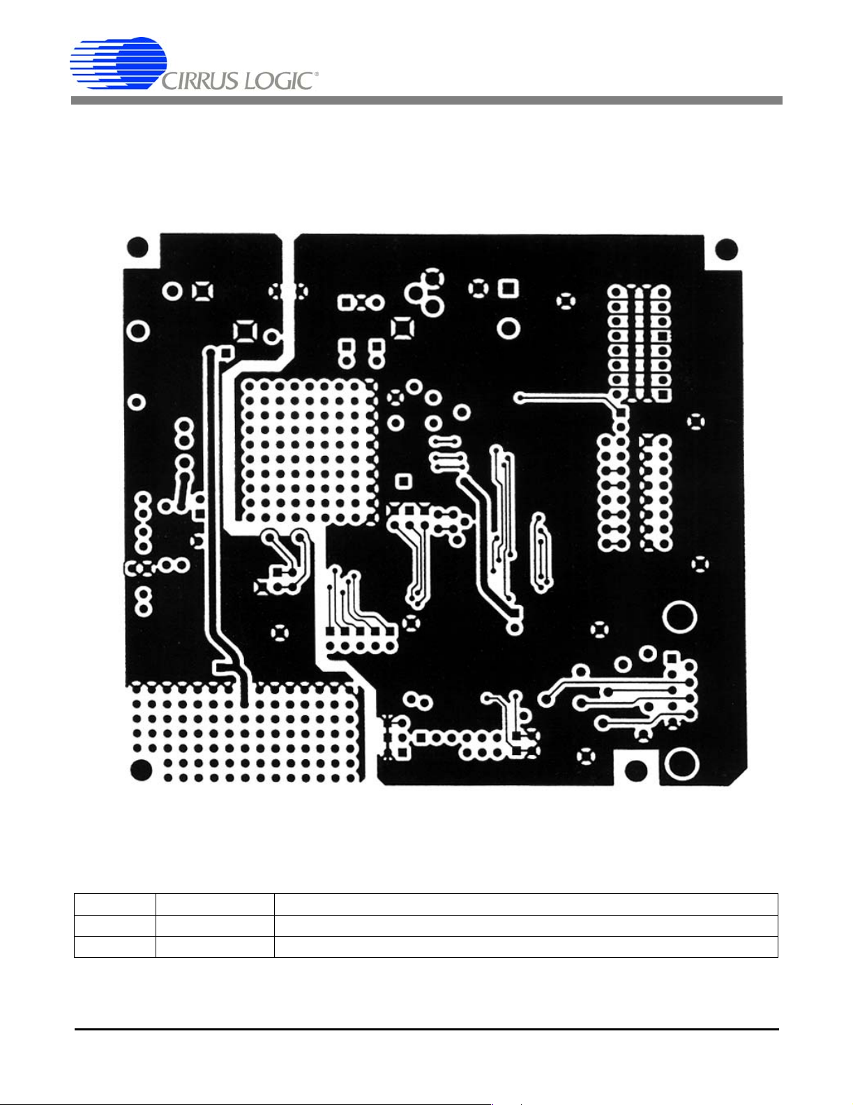
Figure 7. Component-side Trace Layer (Not to Scale)
DS170DB5 9
Page 10
CDB8130
Figure 8. Solder-side Trace Layer (Not to Scale)
2 REVISION HISTORY
Revision Date Changes
DB4 APR 2002 Initial public release
DB5 MAR 2006 Updated company contac t information & legal statement.
10 DS170DB5
 Loading...