Cirrus Logic CS6403-IQ, CS6403-IL, CDB6403 Datasheet
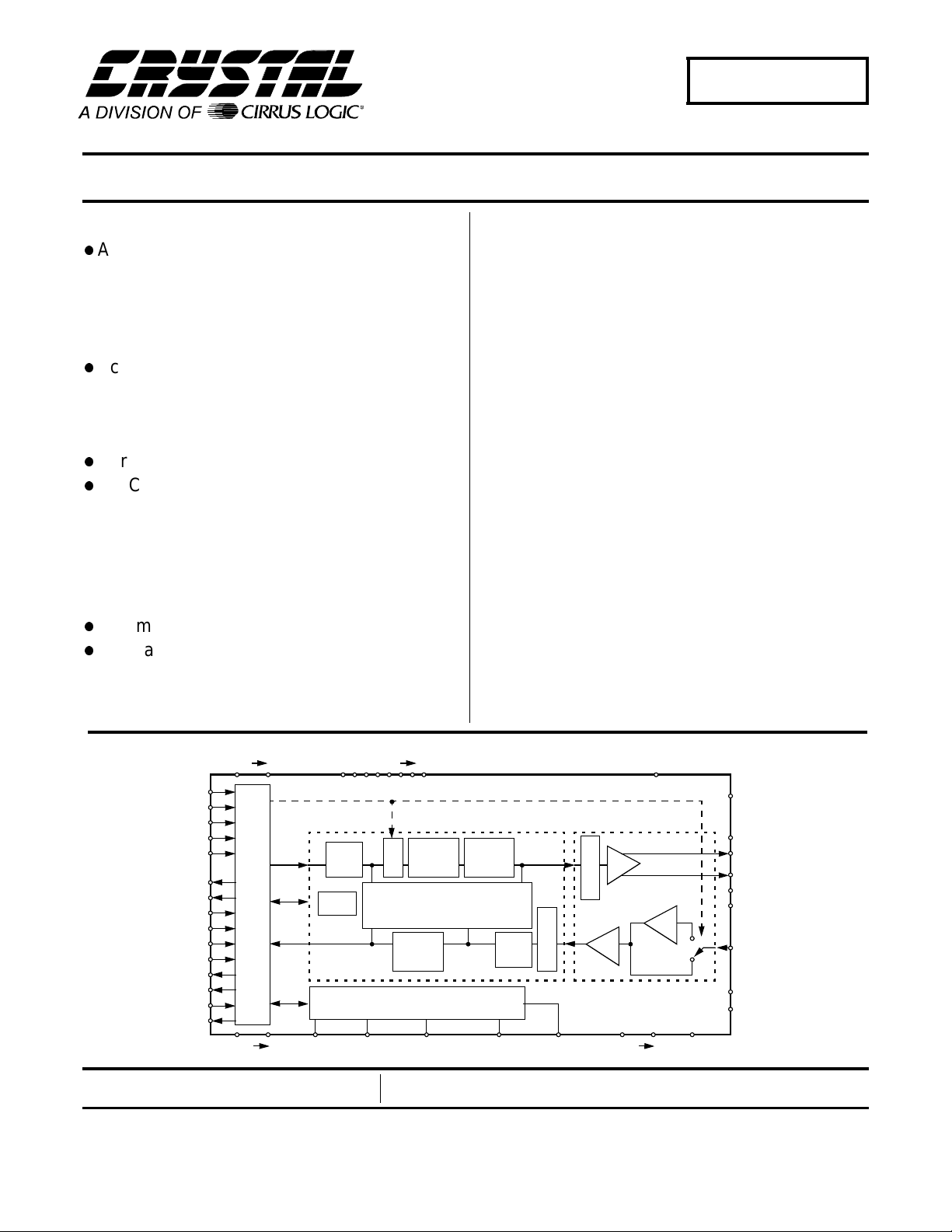
Echo-Cancelling Codec
CS6403
Features
l
Applicable in:
- Digital-Cellular Hands-Free Phones
- Analog-Cellular Hands-Free Phones
- Office Speaker Phones
- Desktop & Video Teleconferencing
l
Echo Cancellation
- Up to 60 dB ERLE
- 512 Tap (64 ms at 8 kHz sampling rate)
- Split Mode For Two Echo Cancellers
l
Serial Data/Control Interface
l
On-Chip Delta-Sigma Codec
- < 1% THD, 8 Ω Load On Output
- > 70 dB S/(N+D) on Input
- 300-3600 Hz Bandwidth (8 kHz sampling rate)
- Volume Control
- Microphone Preamp
l
Automatic Gain Control (AGC)
l
No Training Signals Generated
I
Description
The CS6403 is an application-specific digital signal processor optimized for network and acoustic echo
cancellation applications. A high-quality codec is integrated with the processor to provide a complete, lowcost echo-cancellation solution.
The CS6403 is a fully independent processor that requires no signal processing support to implement its
cancellation functions. Volume control, AGC, and sleep
functions are also prov ided.
The on-chip ADC and DAC employ over-sampling technology, which eliminates the need for complex external
anti-aliasing and reconstruction filters, further reducing
system cost.
The CS6403 has a serial interface that i s compatibl e with
most DSPs and PCM codecs. Clock and sync lines control the tr ansfer of seri al data via the separate ser ial datain and data-out pins. Both 16-bit audio data and control/status information may be multiplexed on this serial
channel using a steering bit.
ORDERING INFORMATION
CS6403-IQ -40° to +85° C 44-pin TQFP
CS6403-IL -40° to +85° C 44-pin PLCC
CDB6403 Evaluation Board
CONFIG
GPIN0
GPIN1
GPIN2
GPIN3
GPOUT0
GPOUT1
SFRAME
SMASTER
UALAW
SSYNC
SCLK
SDO_1
SDI_A
SYNCOUT
DVDD0 1
Serial I/O
DGND0 1
Control
Status
RESERVED0 6
DSP
High
Pass
Control
CLKIN CLKOUTSCLK_RATE0
Preliminary Product Information
Cirrus Logic, Inc.
Crystal Semiconductor Products Division
P.O. Box 17847, Austin, Texas 78760
(512) 445 7222 FAX: (512) 445 7581
http://www.crystal.com
AVDD
Analog I/O
Nonlinear
A
Echo
G
Control
C
Echo Cancellers
Nonlinear
Echo
Control
PLL + Clock Manager
This document contains information for a new product.
Cirrus Logic reserves the right to modify this product without notice.
Volume
Control
High
Pass
SCLK_RATE1
Copyright Cirrus Logic, I nc. 1997
CLK_SEL NC
(All Rights Reserv ed)
A
T
D/A
T
E
N
A
T
T
E
N
A/D
AGND0 1
26 dB
RESET
PVDD
SPKROUTP
SPKROUTN
PGND0
PGND1
MICIN
VCM
VREF
MAR ‘96
DS192PP7
1
CS6403
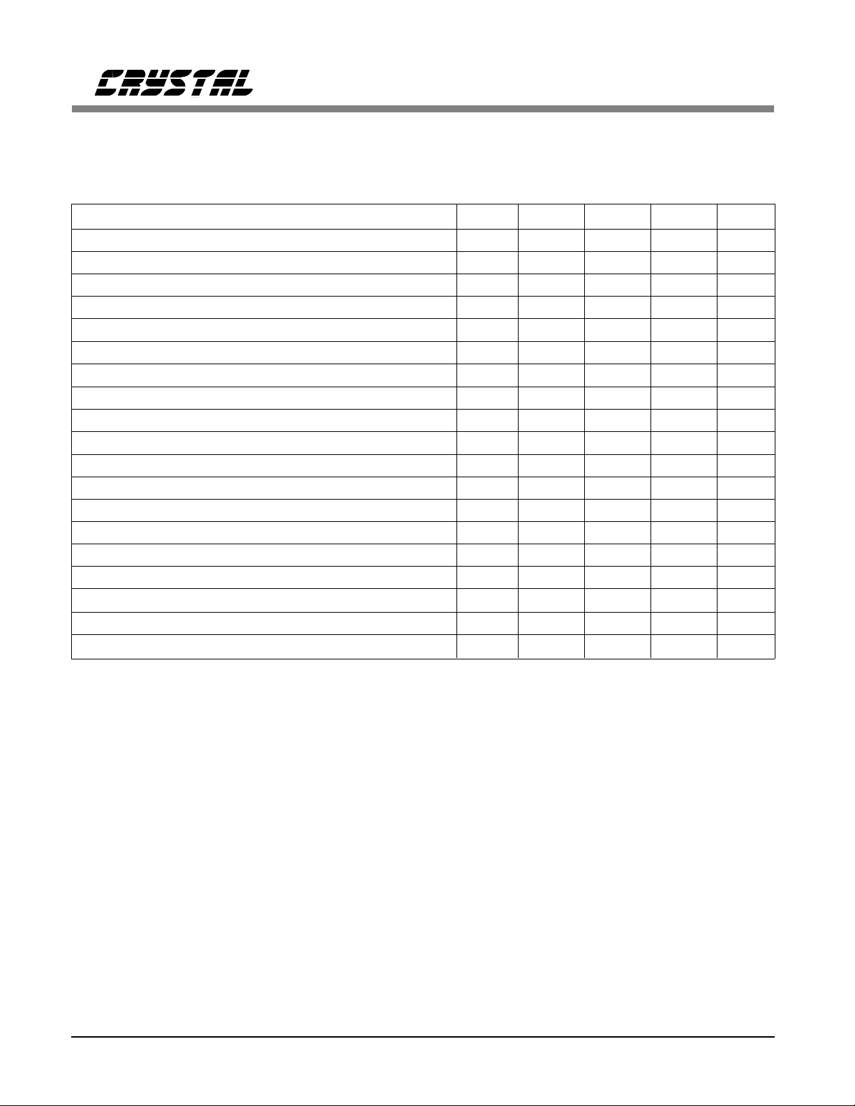
ADC CHARACTERISTICS (T
Logic 0 = 0V, Logic 1 = DVDD; Signal test frequency 1kHz, word rate (Fs) = 8kHz, audio signal measurement
bandwidth is 20Hz to 4kHz; Microphone amp gain = 0dB; SPRKOUT outputs connected to 8Ω load; CLKIN frequency = 8.192MHz; unless otherwise specified) Note 1.
Parameter Symbol Min Typ Max Units
ADC Resolution With No Missing Codes 12 - - bits
Instantaneous Dynamic Range IDR 67 72 - dB
Total Harmonic Distortion at -0.5dBFS signal level THD - 0.01 0.05 %
Gain Drift (Note 2) - 150 - ppm/°C
Offset E rror - 0 2 LSB
Full Scale Input Voltage (Note 3) 0.85 1.0 1.1 V
Input Resistance (at MICIN) (Note 2) 25 - Input Capacitance (at MICIN) (Note 2) - 15 - pF
Sample Rate Fs - 8 - kHz
Microphone Amp Gain (switchable on/off) 24 26 28 dB
Anti-aliasing Rejection - 30 - dB
Power Supply Rejection (1kHz) PSR 40 - - dB
Frequency Response -0.6 - 0.6 dB
Transition Band 0.45 - 0.6 Fs
Stop Band Rejection 70 - - dB
VREF Reference Voltage Output - 2 .0 - V
VCM Voltag e Output constan t load only , >100 kΩ
Group Delay (Note 4) - 1 - ms
Group Delay Variations vs. Frequency (Note 4) - 0.0 -
Notes: 1. Bench testing is done with Crystal part CXT8192 driving CLKIN, automated device testing utilizes
test system provided clock sources.
2. Guaranteed by design/characterization.
3. This is the peak input voltage (in volts) with the mic amp gain set to 0 dB. Peak-to-peak voltage is
2x peak. Input signals will be properly clipped if the peak signal is greater than full scale, but less
than 2x full scale.
4. This group-delay specification is for the ADC only; additional group delay is introduced by the
AGC and high-pass filter that is implemented on the CS6403 in software.
= 25 °C; All DVDD, AVDD, and PVDD = 5.0V, Digital Input Levels:
A
-1.0-V
p
kΩ
µs
2 DS192PP6
CS6403
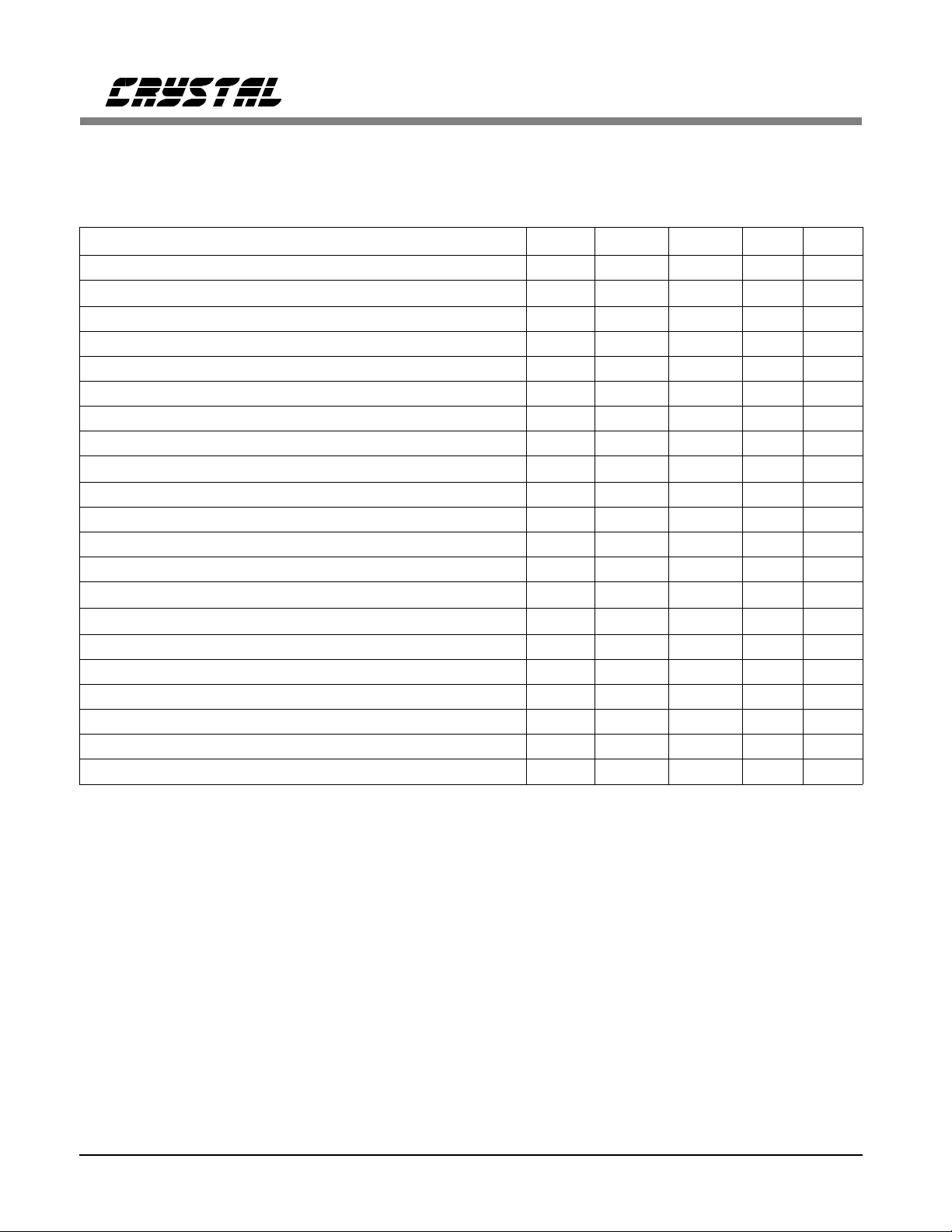
DAC CHARACTERISTICS (T
Logic 0 = 0V, Logic 1 = DVDD; Signal test frequency 1kHz, word rate (Fs) = 8kHz, audio signal measurement
bandwidth is 20Hz to 20kHz; Microphone amp gain = 0dB; SPRKOUT outputs connected to 8Ω load; CLKIN frequency = 8.192MHz; unless otherwise specified)
Parameter Symbol Min Typ Max Units
DAC Resolution 12 - - bits
DAC step size error - Instantaneous Dynamic Range (20 Hz - 20 kHz) IDR 60 72 - dB
Frequency Response -0.8 - +0.6 dB
Programmable Output Level Attenuator Range (Note 5) -92.2 - 0 dB
Gain Step Size - 2.49 - dB
Gain Drift (Note 2) - 150 - ppm/°C
VREF Reference Output Voltage - 2.0 - V
VCM Output Voltage constant load only, >100kΩ
Offset E rror - 25 50 mV
Full Scale Output Voltage (SPKROUT pins) (Note 6) 1.40 1.75 1.93 V
Common Mode Output Voltage (SPKROUT pins) - 1.30 - V
Total Harmonic Distortion at -0.5dBFS level, SPKROUT(Note 9) THD - - 0.8 %
Output Impedance SPKROUT pins - 0 .4 Load Impedance SPKROUT pins 8 - Output Capacitance - 15 - pF
Audible Stop Band Attenuation (<20kHz) 68 - - dB
Integrated Inaudible Energy (>20kHz to 100kHz) (Note 7) - - 30 mVrms
Power Supply Rejection (1kHz) PSR 40 60 - dB
Filter Transition Band 0.45 - 0.6 Fs
Group Delay (Note 8) - 1 - ms
Notes: 5. Attenuation settings greater than 92.2 dB will cause a full scale input signal to be completely
attenuated to zero signal level.
6. This is the peak differential output voltage. The peak-to-peak signal level on each output pin is
equal to the peak differential value.
7. Assuming an external 43.2 kHz RC output filter.
8. This group-delay specification is for the DAC only; additional group delay is introduced by the
AGC and high-pass filter that is implemented on the CS6403 in software.
9. Room temperature only.
= 25 °C; All DVDD, AVDD, and PVDD = 5.0V, Digital Input Levels:
A
±0.5
-1.0-V
LSB
p
Ω
Ω
DS192PP6 3
CS6403
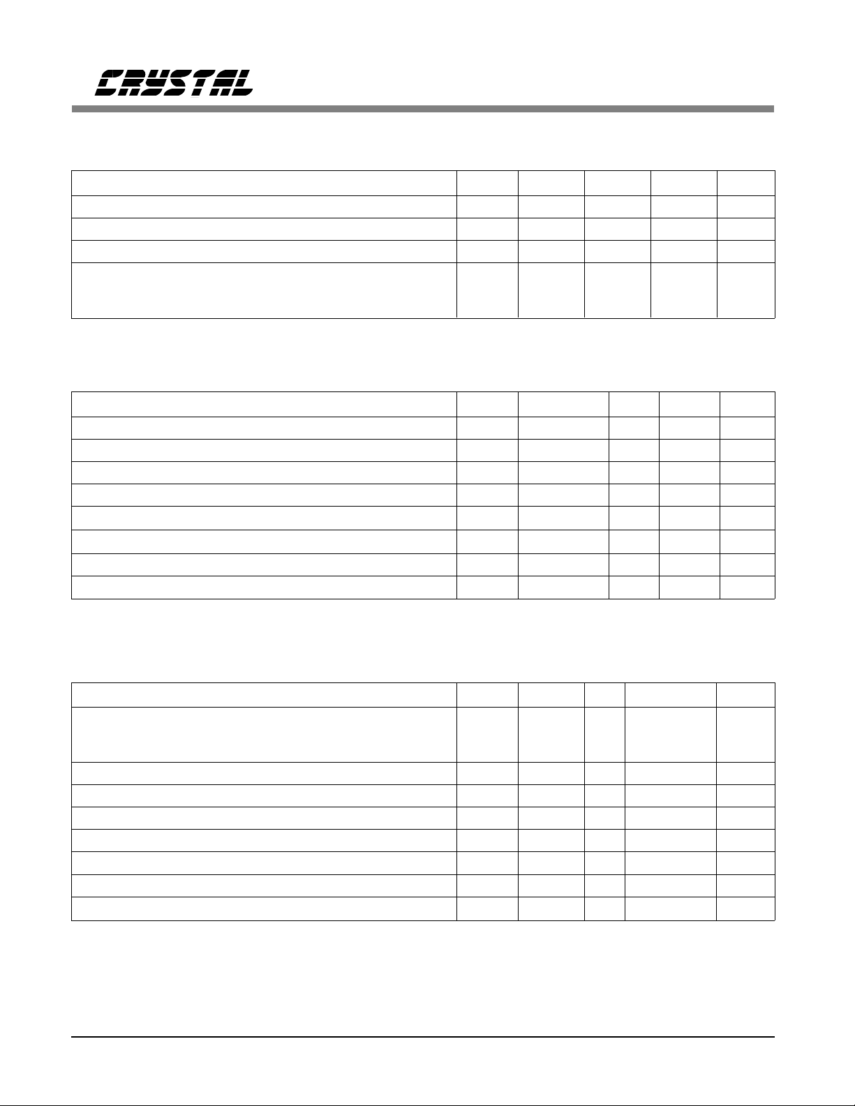
PHASE-LOCKED LOOP CHARACTERISTICS (T
= 25°C; AVDD, DVDD, and PVDD = +5V;
A
Input Levels: Logic 0 = 0V, Logic 1 = DVDD)
Parameter Symbol Min Typ Max Units
PLL acquisition time T
ACQ
0.3 1 ms
PLL frequency range 23.35 24.58 25.80 MHz
PLL jitter 200 ps rms
Input ref frequency 1.95
0.97
243
DIGITAL CHARACTERISTICS (T
= 25°C; AVDD, DVDD, and PVDD = 5V)
A
2.048
1.024
256
2.15
1.08
268
MHz
MHz
kHz
Parameter Symbol Min Typ Max Units
High-level Input Voltage V
Low-level Input Voltage V
High-level Output Voltage at I0 = -2.0 mA V
Low-level Output Voltage at I0 = +2.0 mA V
Input Leakage Current (Digital Inputs) I
OH
OL
IN
Output Leakage Current (High-Z Digital Outputs) - - 10
Output Capacitance (Note 2) C
OUT
Input Capacitance (Note 2) C
DVDD - 1.0 - - V
IH
IL
--1.0V
DVDD - 0.3 - - V
--0.3V
--10
--15pF
IN
--15pF
µA
µA
ABSOLUTE MAXIMUM RATINGS (All voltages with respect to 0V)
Parameter Symbol Min Typ Max Units
Power Supplies AVDD
DVDD
PVDD
Input Current Except Supply Pins & Driver Pins I
Short Circuit Current Limit SPKROUT pins (Note 10) I
Analog Input Voltage V
Digital Input Voltage V
Ambient Temperature (Power Applied) T
Storage Temperature T
ESD using human body model (100pF with series 1.5kΩ)
IN
SC
INA
IND
AMAX
STG
V
ESD
Notes: 10. SPKROUTP or SPKROUTN shorted to ground.
Warning: Operation beyond these limits may result in permanent damage to the device.
Normal operation is not guaranteed at these extremes.
4 DS192PP6
-0.3 - 6.0 V
--10.0mA
- - 500 mA
-0.3 - AVDD + 0.3 V
-0.3 - DVDD + 0.3 V
-55 - 125 °C
-65 - 150 °C
2000 - - V
CS6403
POWER CONSUMPTION (T
1kHz; Word Rate (Fs) = 8kHz; SPRKOUT outputs connected to 8Ω load; Mode 2 SCLK = 256 kHz; unless otherwise specified) Full scale output.
Parameter Symbol Min Typ Max Units
Normal Operation Power Dissipation P
High-Impedance Output (Note 11) P
RESET High P
RESET High, clocks halted (Note 12) P
Powerdown Asserted in Software P
Notes: 11. SPKROUT outputs connected to 1 kΩ load.
12. RESET high, CLKIN grounded (Mode 1) or SCLK grounded (Mode 2), and CLK_SEL (PIN 15Q, 21L)
high to disable PLL.
= 25°C; All DVDD, AVDD and PVDD = 5.0V; Signal test frequency
A
D
NS
RH
RNC
PDN
- 800 - mW
- 300 - mW
-55-mW
-15-mW
-55-mW
RECOMMENDED OPERATING CONDITIONS (All voltages with respect to 0V)
Parameter Symbol Min Typ Max Units
DC Power Supplies: AVDD
DVDD
PVDD
Ambient Operating Temperature T
A
4.50 5.0 5.50 V
-40 85 °C
t
t
ckl
ckh
CLKIN
t
pd3
SCLK
SYNCOUT
(Master Mode)
SCLK & SYNCOUT Output Timing
Mode 1 - MASTER
DS192PP6 5

CS6403
SWITCHING CHARACTERISTICS (T
= 25°C; AVDD and DVDD = +5V, output loaded with
A
30 pF; Input Levels: Logic 0 = 0V, Logic 1 = DVDD)
Parameter Symbol Min Typ Max Units
Mode 1 - MASTER
Input clock (CLKIN) frequency CLKIN 7.78 8.192 8.60 MHz
CLKIN low time t
CLKIN high time t
ckl
ckh
30 - - ns
30 - - ns
Sample Rate Fs - 8 - kHz
SCLK and SYNCOUT output delay from CLKIN rising t
SCLK duty cycle (Note 12) t
SCLK rising to SYNCOUT rising t
SCLK rising to SYNCOUT falling t
SDO delay from SCLK edge t
SDI setup time to SCLK edge t
SDI hold time from SCLK edge t
SDO to Hi-Z state t
SDO to non-Hi-Z bit 1 t
pd3
sckw
sr1
sf1
pd1
s1
h1
hz
nz
RESET pulse width high 250 - -
- - 50 ns
-50-%
-1230ns
- 6 30 ns
- - 70 ns
15 - - ns
10 - - ns
- - 50 ns
5--ns
µs
Mode 2 - SLAVE
Input clock (SCLK) frequency SCLK 243
0.97
1.95
SCLK low time t
SCLK high time t
SYNCOUT output delay from SSYNC rising t
SYNCOUT output delay from SSYNC falling t
ckl
ckh
pdsr
pdsf
150 - - ns
150 - - ns
- - 50 ns
- - 50 ns
256
1.024
2.048
268
1.08
2.15
kHz
MHz
MHz
Sample Rate Fs - 8 - kHz
SDI/SSYNC setup time to SCLK edge t
SDI/SSYNC hold time from SCLK edge t
SDO delay from SCLK edge t
SDO to Hi-Z state bit 16/8 t
SDO to non-Hi-Z bit 1 t
s1
h1
pd1
hz
nz
RESET pulse width high 250 - -
15 - - ns
10 - - ns
- - 70 ns
- - 50 ns
5--ns
µs
Notes: 12. When the CS6403 is in master mode (SSYNC and SCLK outputs), the SCLK duty cycle is 50%.
The period of SCLK is 4/CLKIN.
6 DS192PP6
t
A
A
A
A
A
A
A
A
A
A
A
A
A
A
A
A
A
A
A
A
A
A
A
A
A
A
A
A
A
A
A
A
A
A
A
A
A
A
A
A
A
A
A
A
A
A
A
A
A
A
A
A
A
A
A
A
A
A
A
A
A
A
A
A
A
A
A
A
A
A
A
AAA
A
A
A
A
A
A
A
A
A
A
A
A
A
A
A
A
A
A
A
A
A
A
A
A
A
A
A
A
A
A
A
A
A
A
A
A
A
A
A
A
A
A
A
A
A
A
A
A
A
A
A
A
A
A
A
A
A
A
A
A
A
A
A
A
A
A
A
A
A
A
A
AAA
A
A
A
A
A
A
A
A
A
A
A
A
A
A
A
A
A
A
A
A
A
A
A
A
A
A
A
A
A
A
A
A
A
A
A
A
A
A
A
A
A
A
A
A
A
A
A
A
A
A
A
A
A
A
A
A
A
A
A
A
A
A
A
A
A
A
A
A
A
A
A
A
A
A
A
A
A
A
A
A
A
A
A
A
A
A
A
A
A
A
A
A
A
A
A
A
A
A
A
A
A
A
A
A
A
A
A
A
A
A
A
A
sckw
SCLK
t
t
sr1
sckhtsckl
t
sf1
SYNCOUT
(Short Frame)
t
sr1
SYNCOUT
1
(Long Frame)
t
h1
t
s1
SDI
t
nz
Bit 1 Bit 2 Bit 7 Bit 8
t
pd1
t
pd1
SDO
Note: 1. SYNCOUT is long frame when SFRAME = 1.
Master Mod e Seria l Port Tim ing
(Mode 1)
CS6403
AA
AA
AA
AA
AA
AA
AA
AA
AA
AA
AA
AA
AA
AA
AA
AA
AA
AA
AA
AA
AA
AA
AA
AA
AA
AA
AA
AA
AA
AA
AA
AA
AA
AA
AA
AA
AA
AA
AA
AA
AA
AA
AA
AA
AA
AA
AA
AA
AA
AA
AA
AA
AA
AA
AA
AA
AA
AA
AA
AA
AA
AA
AA
AA
AA
AA
AA
AA
AA
AA
AA
AA
AA
AA
AA
AA
AA
AA
AA
AA
AA
AA
AA
AA
AA
AA
AA
AA
AA
AA
AA
AA
AA
AA
AA
AA
AA
AA
AA
AA
AA
AA
AA
AA
AA
AA
AA
AA
AA
AA
AA
AA
AA
AA
AA
AA
AA
AA
AA
AA
AA
AA
AA
AA
AA
AA
AA
AA
AA
AA
AA
AA
AA
AA
AA
AA
AA
AA
AA
AA
AA
AA
AA
AA
Bit 8Bit 7Bit 1 Bit 2
t
sf1
t
hz
t
sckhtsckl
SCLK
th1t
s1
SSYNC
t
pdsf
t
pdsr
DS192PP6 7
SYNCOUT
SDI
SDO
t
h1
t
s1
Bit 1 Bit 2
t
pd1
t
nz
t
pd1
Bit 1 Bit 2
Slave Mode Serial Port Timing
AA
AA
AA
AA
AA
AA
AA
AA
AA
AA
AA
AA
AA
AA
AA
AA
AA
AA
AA
AA
AA
AA
AA
AA
AA
AA
AA
AA
AA
AA
AA
AA
AA
AA
AA
AA
AA
AA
AA
AA
AA
AA
AA
AA
AA
AA
AA
AA
AA
AA
AA
AA
AA
AA
AA
AA
(Mode 2)
AA
AA
AA
AA
AA
AA
AA
AA
AA
AA
AA
AA
AA
AA
AA
AA
AA
AA
AA
AA
AA
AA
AA
AA
AA
AA
AA
AA
AA
AA
AA
AA
AA
AA
AA
AA
AA
AA
AA
AA
AA
AA
AA
AA
AA
AA
AA
AA
AA
AA
AA
AA
Bit 15
AA
AA
AA
(Bit 7)
AA
Bit 15
(Bit 7)
Bit 16
(Bit 8)
Bit 16
(Bit 8)
t
hz
60.0
40.0
CS6403
ERLE
ERLE (dB)
20.0
Speech Training Signal
0.0
0.02.04.06.08.0
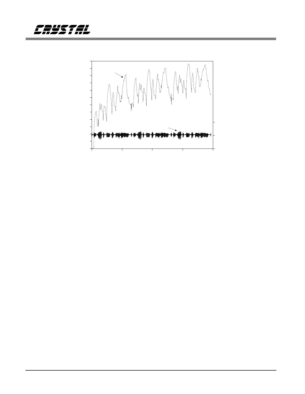
Figure 1 . Typ ical ER LE Conv ergen ce Chara cter istics
Echo Canceller Characteristics
The typical Echo Return-Loss Enhancement
(ERLE) convergence characteristics for the
CS6403 are illustrated in the above diagram
under the following conditions:
• Echo-canceller l ength: 512 taps
• Echo-canceller initial conditions: zeroed filter
taps, updates disabled unt il t=0.12 5s
• Sampling rate : 8 kHz
• Echo path (in cludin g micropho ne, speaker,
and amplifiers):
- spectrally flat
-linear
- duration < 64 ms
- noise free
- time invariant
Speech (mV)
0.3
0.0
-0.3
Seconds
• Near-end high-pass filter: enabled
• Pre-emphas is fil ter: ena bled
• Graded-beta profile: 64 echo-canceller filter
taps pr ocessed per 2 x red uction in upd ate g ain
• Train ing si gna l: spe ech, fu ll sca le
• Unlimited S/(N+D) on linear ADC
Note: Many of these conditions may be
significantly different in real
appl icatio ns, re sulti ng i n sign ific antly
different measured ERLE performance.
8 DS192PP6
CS6403
OVERVIEW
In hands-free speakerphones, the signal from the
far end may echo about the near-end environment and then be received at the near-end
microphone. When heard at the far end, this
echo signal can be very annoying, particularly if
the signal is delayed by transmission or signalprocessing delays.
Voice switching is a particularly simple technique for eliminating this echo, but since it
imposes half-duplex communication, it seriously
compromises conversation quality.
Echo cancellation can provide high-quality, fullduplex communication, but typically must be
implemented using expensive digital signal-processing hardware.
NC
CLK_SEL
CLKIN CLKOUT
Echo Cancellation in the CS6403
The CS6403 provides high-quality echo cancellation at low cost. This breakthrough in
cost/performance is made possible on the
CS6403 by custom, application-optimized processing blocks, which are integrated on a single
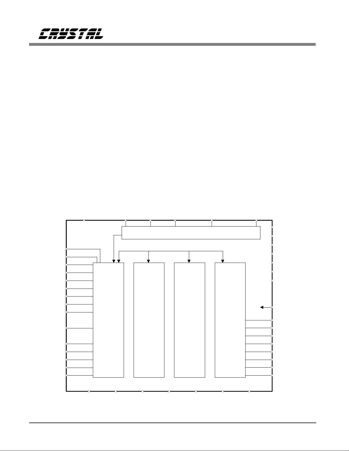
die, as shown in Figure 2.
One of these processing blocks is the AFP
(Adaptive Filter Processor). This block implements a 512-tap AFIR (Adaptive Finite
Impulse-Response) filter which is updated using
an enhanced least-mean squared (LMS) algorithm. At a sampling rate of 8 kHz, it can cancel
up to 64 ms of echo. By default, 10 ms of the
available 64 ms are allocated to a network canceller (NEC), and the remaining 54 ms are
allocated to an acoustic echo canceller (AEC).
SCLK_RATE0 SCLK_RATE1
CONFIG
GPIN0
GPIN1
GPIN2
GPIN3
GPOUT0
GPOUT1
SCLK
SDI
SDO
SFRAME
SMASTER
SSYNC
SYNCOUT
UALAW
PLL/Oscillator
SSI CPU AFP CO DEC
RESERVED0
RESERVED1
RESERVED2
RESERVED3
RESERVED4
RESERVED5
RESERVED6
RESET
AGND0
AGND1
AVDD
MICIN
SPKROUTP
SPKROUTN
VCM
VREF
DVDD0
DVDD1 DGND1 PVDD PGND0 PGND1
DGND0
Figure 2. CS6403 Internal Block Diagram
DS192PP6 9
CS6403
AAAA
AAAA
AAAA
AAAA
AAAA
AAAA
CS6403
DSP or
PCM Codec
Far-End Input
Far-End Output
SDI
SDO
High Pass
Filter
+
Network
Canceller
Echo
AGC/
Volume
Control
-
Non-linear
Echo
Control
Figure 3. Functional Diagram
The Central Processing Unit (CPU) does all the
other miscellaneous processing, like update control and double talk detection. This processing
has a critical influence on overall echo-cancellation performance. Double-talk detection is a
particularly important part of this processing.
Double-talk detection and other algorithms were
carefully developed and validated at Crystal under real-world conditions.
To increase the CS6403’s echo return-loss enhancement (ERLE), supplemental echo
suppression is used. A sophisticated voice-detection algorithm is used to reduce echo with
minimal impact on conversation quality, assuring
the highest quality conversation.
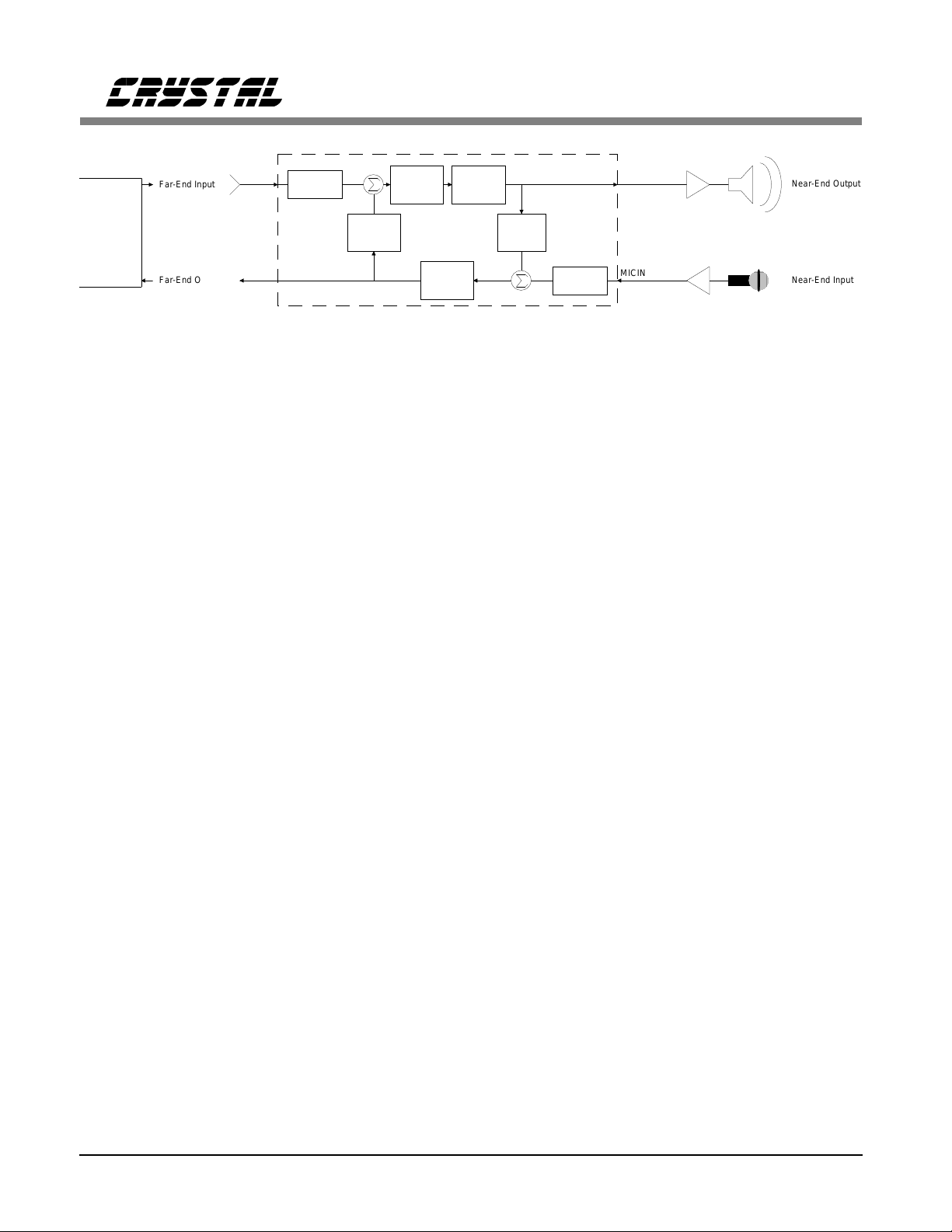
Figure 3 describes the functional behavior of the
CS6403 in a typical application. Digital data
from the far-end interface comes into SDI of the
CS6403 where it is acted upon by the various
algorithms running in the CPU. First, a HighPass Filter eliminates DC offset and low
frequency noise before sending the far-end input
data onto the summing node for the network
echo canceller. Assuming there is no speech
from the near-end, the signal after the summing
node is unaffected.
The signal then passes on to the AGC/Volume
Control block where the signal level is boosted,
if necessary. The volume control is implemented
in part by the AGC (for more details, see the
section entitled "Embedded Signal Processing
Functions").
Non-linear
Echo
Control
Acoustic
Echo
Canceller
+
High Pass
Filter
SPKROUT
MICIN
*
*
* Optional
The signal then passes on to the Non-linear Echo
Control block which controls the half-duplex
failsafe and the supplementary echo suppressor
which act to enhance and supplement the performance of the echo canceller.
The signal after this block is then fed to both the
speaker output and the input to the acoustic echo
canceller (implemented by the AFP). The
speaker output couples to the microphone input
by various echo paths. The signal received at
the microphone is then filtered and sent on to the
summing node of the Acoustic Echo Canceller.
The Acoustic Echo Canceller constructs a model
of the echo paths between the speaker and microphone and processes its input signal with its
digital representation of the echo paths. As such,
its output should very closely match the input
from the microphone and so the output from the
summing node should be a very small signal,
which is referred to as the "error signal." This
error signal is fed back to the echo canceller to
let it adapt its performance should there be a
change in the echo path.
The Non-linear Echo Control block following
the summing node further attenuates any vestiges
of signal received at the microphone that originated from the speaker. This signal is then sent
to the far-end output by SDO as well as to the
input of the Network Echo Canceller, where a
function similar to that performed by the Acoustic Echo Canceller is performed.
Near-End Output
Near-End Input
10 DS192PP6

CS6403
Analog Interface
The codec block provides an analog-to-digital
converter (ADC) and a digital-to-analog converter that can be connected directly to a
microphone and a speaker, respectively.
The output of the microphone should be lowpass filtered, then AC-coupled to the audio input,
MICIN. A 26 dB gain stage is included in the
CS6403 at the ADC input to amplify the microphone signal. However, this gain stage may be
bypassed in modes in which a line-level source
is connected to the CS6403 instead of a microphone. The CS6403 also includes a speaker
driver, which can drive an 8Ω speaker directly,
or alternatively, it can drive a high-impedance
differential input on an external amplifier.
With the 26 dB gain stage on, the fullscale input
for the MICIN pin is 100mV peak-to-peak. Any
signal over 100mV peak-to-peak will clip the input to the ADC. With the gain stage off, a 2V
peak-to-peak signal is the maximum allowed.
The fullscale output voltage from the DAC is
1.75V peak-to-peak single-ended, or 3.5V peakto-peak differentially.
SCLK
SMASTER
0 0 0 256 kHz I slave
0 0 1 undefined
0 1 0 1.024 MHz I slave
0 1 1 2.048 MHz I slave
SCLK_RATE1
SCLK_RATE0
Clock Rate I/O mode
It is very important to not clip signals anywhere
in the system. An echo canceller can only remove echo that passes through a linear, time
invariant path. Echo that passes through a nonlinearity (like clipping) will not be removed by
the echo canceller.
Both the DAC and ADC paths are bandlimited
as a function of sampling rate. At a sampling
rate of 8 kHz, the paths are limited to 03600 Hz.
Synchronous Serial Interface
The Synchronous Serial Interface (SSI) provides
a data and control interface to the CS6403. The
SSI can be connected to an external network
codec for applications like speakerphones or to a
DSP for high-end applications like video teleconferencing.
Depending on the state of the SMASTER
(PIN 42Q, 4L) pin at RESET, the CS6403 can
operate as either a system timing master or slave.
As a master, the serial clock pin (SCLK) is an
output. As a system timing slave, SCLK must
be driven by an external source. When SMASTER is high, the SCLK output frequency is a
fixed 2.048 MHz derived from the 8.192 MHz
crystal oscillator connected across CLKIN and
CLKOUT. When SMASTER is low, internal
timing is generated by the Phase Locked Loop
(PLL), which uses SCLK’s input as a timing reference, so no external crystal is necessary. In
slave timing mode, SCLK can be driven at 256
kHz, 1.024 MHz, or 2.048 MHz. The CS6403 is
informed of the SCLK rate via the
SCLK_RATE0 (PIN 29Q, 35L) and
SCLK_RATE1 (PIN 30Q, 36L) pins.
1 0 0 undefined
1 0 1 undefined
1 1 0 undefined
1 1 1 2.048 MHz O master
Table 1 shows the various options for SCLK.
Table 1. Clock Options
DS192PP6 11

CS6403
Configuration
Mode 1: Master Interface (e.g. CODEC⇔CS6403)
Application: Low-cost speaker phone
1.1: Short-Frame Mode 0 1 0
1.2: Long-Frame Mode 1 1 0
Mode 2: Slave Interface (e.g. DSP⇔CS6403)
Application: Digital cellular
2.1: 16-bit Mode 0 0 1
2.2: 8-bit Mode 0 0 0
Table 2. CS6403 Configurations
Mode Selection
The behavior of the CS6403 is controlled by
configuration-control input pins. The behavior of
the CS6403 for each possible state of these control signals is illustrated in Table 2.
As indicated in Table 2, the CS6403 has two basic operating modes. These operating modes are
illustrated in Figure 4.
The simplest operating mode is Mode 1. This
operating mode is useful in applications where
the data link to the far end is analog, as in analog cellular hands free, or in analog speaker
phones. The SSI is the system timing master in
Mode 1. Long or short framing signals can be
generated. Word length is always 8 bits.
SFRAME
SMASTER
CONFIG
Mode 2 is useful in applications where the data
link to the far end is digital, as in digital cellular
hands free, or in digital (ISDN) speaker phones.
The SSI is the system timing slave in Mode 2.
Only short framing pulses are accepted. Word
length can be 8 or 16 bits. Mode 2 allows access to control registers in 16-bit Mode.
States of Operation
Reset
Reset may be asserted either by setting the RESET (PIN 41Q, 3L) pin high, or by setting the
Reset bit in Synchronous Serial Interface Control
Register 0 (RST: SSI_CR0.11). The only functional difference between these two operations is
that setting the RESET pin clears the RST bit.
During Reset, all chip functions are halted ex-
Codec
Far End Near End
DSP
CS6403
Mode 1
CS6403
Mode 2
Figure 4. Operating Modes
12 DS192PP6
CS6403
cept for the SSI, though writes to any control bit
except RST are ignored. Power down is not enabled.
Upon exiting Reset, control registers and RAM
are cleared, and then control constants are loaded
into Data RAM from the Program ROM.
External
µ
-law
Codec
Digital
Ground
FSR
FST
BCLKR
BCLKT
MCLK
DR
DT
+
1 µF
0.1 µF
Analog
Ground
SYNCOUT
SCLK
SSYNC
SDO
SDI
RESERVED1
SCLK_RATE0
SCLK_RATE1
SMASTER
SFRAME
UALAW
CLK_SEL
CONFIG
GPIN0
GPIN1
GPIN2
GPIN3
RESERVED0
RESERVED2
RESERVED3
RESERVED4
RESERVED5
RESERVED6
DVDD0
DVDD1
DGND1
DGND0
Speaker
Ground
RESET
CS6403
System
Reset
AGND1
Power-Down
Power Down is initiated by setting the Sleep bit
in SSI Control Register 0 (SLP: SSI_CR0.10).
In Power Down, the CPU and the AFP are powered down, but the SSI and the Codec are still
operational. Power Down is only accessible in
Mode 2 (16-bit).
Since the SSI and the Codec are active during
Power Down, it is possible to serially transfer
SPKROUTP
SPKROUTN
GPOUT0
GPOUT1
CLKOUT
PGND0
PGND1
AGND0
VREF
VCM
NC
MICIN
CLKIN
PVDD
AVDD
470 pF
0.1µF
0.1µF
F0.1 µF0.1
0.1
µ
0.1
8
Ω
+
1µF
+
1µF
Microphone
Phantom Power
Supply
33 pF
33 pF
µ
Φ0.1 µΦ
2.2k
0.47µF
150
Ω
F
0.022
µ
NPO
8.192MHz
++
µ
F
Ω
Microphone
+5V Analog
Supply
+
10 µF
2
Ω
Figure 5. External Mu-law Codec Connection Diagram
DS192PP6 13

CS6403
audio and control data while SLP is asserted, bypassing the CPU and AFP. Note, however, that
since the CPU is powered down, no scaling is
performed on the ADC input, no echo is cancelled, and audio data is not companded.
Using the CS6403
Interfacing as a Master to an external codec
(Mode 1)
In applications like speakerphones, it is possible
to connect the CS6403 directly to an external
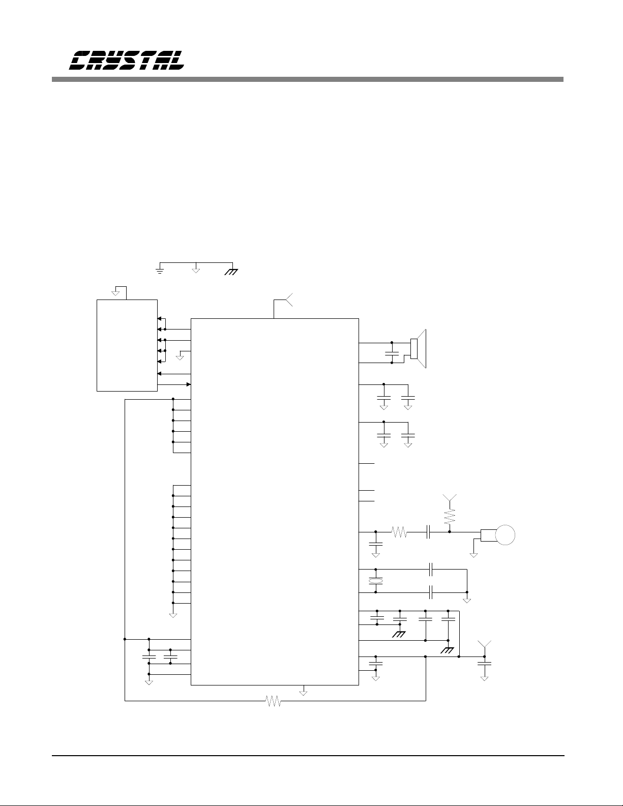
network codec. An example circuit is shown in
Figure 5.
Mode 1.1 (Short-Frame Mode)
SFRAME=0; SSYNC = 0
In this application, SYNCOUT and SCLK are
sourced by the CS6403 (i.e., SMASTER=1), and
CLKIN is generated by connecting a crystal between CLKOUT and CLKIN. The timing for
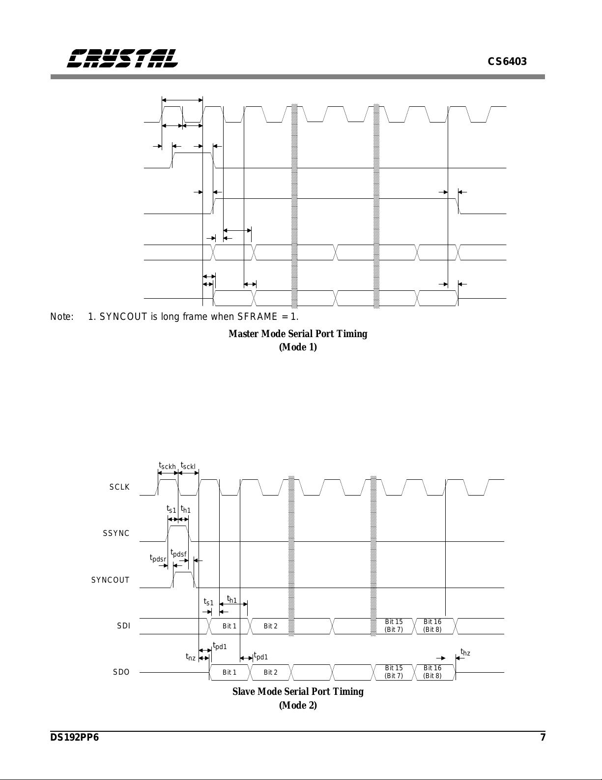
these signals is illustrated in Figure 6.
Audio-data samples in Mode 1 are 8 bits and are
µ−law or A-law companded depending on the
state of the UALAW pin (PIN 13Q, 19L). No
control information can be transferred in Mode
1, so there is no control/data steering bit. Also
note that since control information cannot be
transferred, the default settings of the control
registers established after Reset are used.
In Mode 1, 80 echo-canceller taps (out of the
available 512) are permanently allocated to network-echo cancellation (see Figure 3).
SCLK (out)
SYNCOUT (out: 8kHz)
SDI (in)
SDO (out)
Mode 1.2 (Long-Frame Mode)
SFRAME=1; SSYNC = 0
SCLK (out)
SYNCOUT (out: 8kHz)
SDI (in)
SDO (out)
b7 b6 b5 b4 b3 b2 b1 b0
b7 b6 b5 b4 b3 b2 b1 b0
b7 b6 b5 b4 b3 b2 b1 b0
b7 b6 b5 b4 b3 b2 b1 b0
Figure 6. External-Codec Mode Timing (Mode 1)
14 DS192PP6
CS6403
Interfacing as a Slave to an external DSP
(Mode 2)
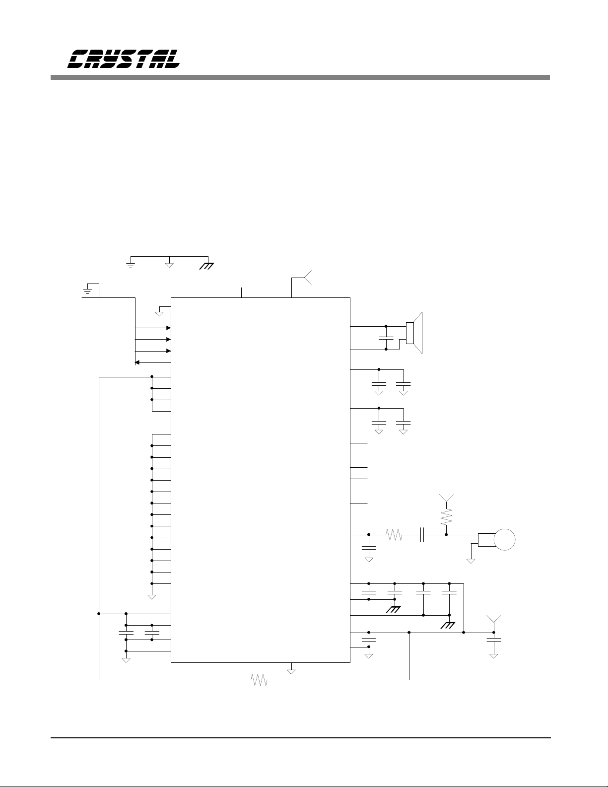
When interfacing to an external DSP (Mode 2),
the CS6403 is configured as a slave to the DSP:
SSI; i.e., SCLK, and SSYNC signals are provided to the CS6403 by the DSP. An example of
the interface circuitry is shown in Figure 7.
Speaker
Ground
CLKIN CLKOUT
SDI
SCLK
SSYNC
SDO
CONFIG
RESERVED1
SCLK_RATE0
SCLK_RATE1
CS6403
RESET
DSP
Digital
Ground
Analog
Ground
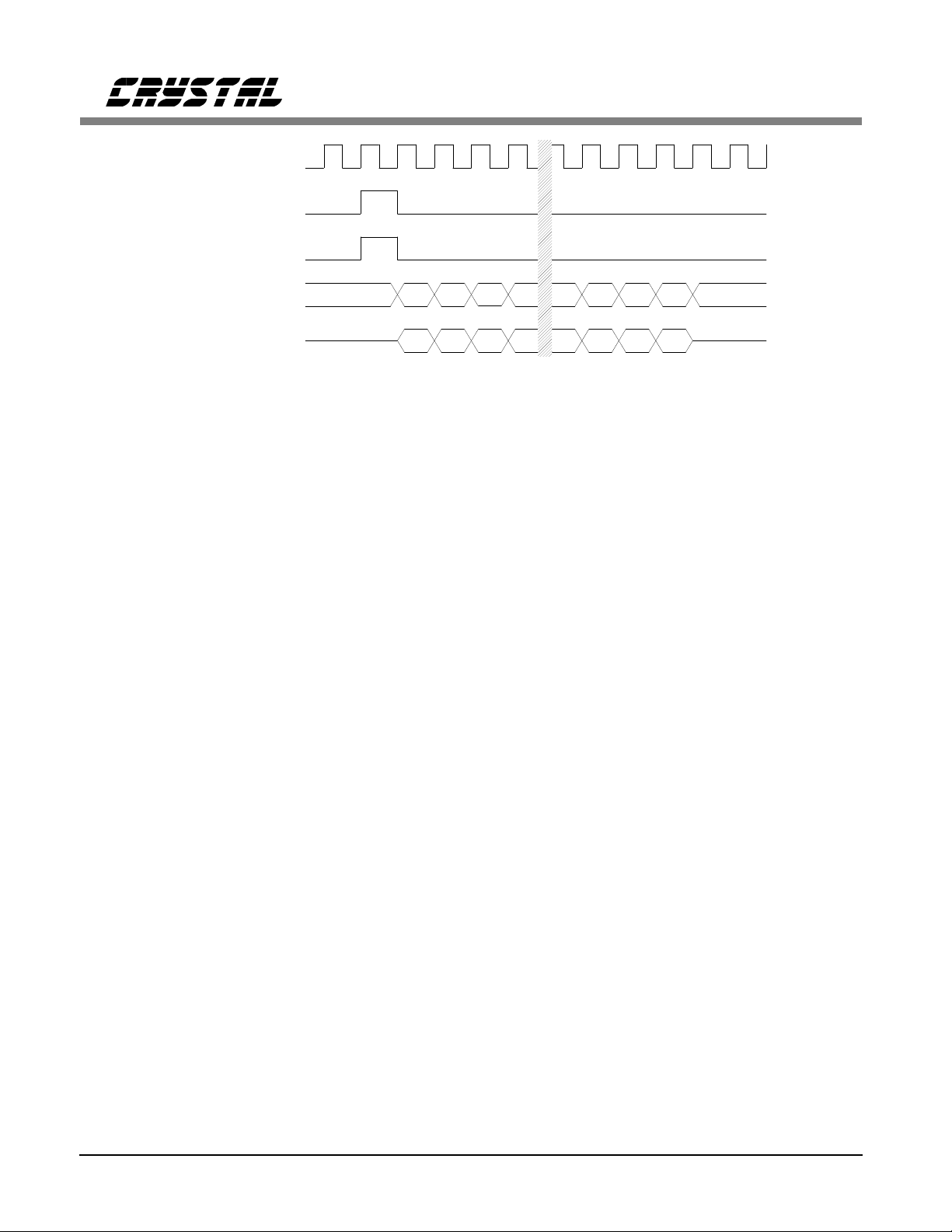
In this case, the DSP sends a single start-offrame pulse to the SSYNC input one SCLK
period before the start of a data frame. Since
there is only one SSYNC input, every data frame
includes both a data read from the CS6403 and a
data write to the CS6403. The behavior of the
serial interface is illustrated in Figure 8.
System
Reset
SPKROUTP
SPKROUTN
VREF
VCM
470 pF
0.1
µ
0.1
µ
8
Ω
+
F
F
+
1 µF
1
µ
F
1 µF
CLK_SEL
GPIN0
GPIN1
GPIN2
GPIN3
RESERVED0
RESERVED2
RESERVED3
RESERVED4
RESERVED5
RESERVED6
SFRAME
SMASTER
UALAW
0.1 µF
+
DVDD0
DVDD1
DGND1
DGND0
AGND1
2
Ω
NC
GPOUT0
GPOUT1
SYNCOUT
MICIN
PVDD
PGND0
PGND1
AVDD
AGND0
0.1
µ
0.022
NPO
F
0.1
150
0.1
µ
0.47µF
Ω
µ
F
F
µ
F
Microphone
Phantom Power
Supply
0.1
F
0.1
µ
++
2.2k
F
µ
Ω
Microphone
+5V Analog
Supply
+
10
F
µ
Figure 7. DSP Connection Diagram (Mode 2)
DS192PP6 15
SCLK (in)
SSYNC (in)
SYNCOUT (out)
SDI (in) b15 b14 b13 b12 b3 b2 b1 b0
SDO (out) b15 b14 b13 b12 b3 b2 b1 b0
Figure 8. Serial Port Timing for Mode 2 (16-bit) - SLAVE
CS6403
Mode 2 (8-bit) Slave
Mode 2 (8-bit) provides a slaved SSI which may
be needed for 8-bit companded audio interfacing,
as is the case with many ISDN transceivers.
Mode 2 (8-bit) timing is similar to Mode 2 (16bit) timing, but the serial data is 8-bit
companded, with the type of companding determined by the state of the UALAW pin. All 8
bits are used for audio, so no steering bit is necessary, and consequently, no control information
can be transferred in this mode.
Mode 2 (8-bit) is selected by setting CONFIG
low, as opposed to high in Mode 2 (16-bit). See
Table 2 for more details. SCLK frequency is determined by the SCLK_RATE1 and
SCLK_RATE0 pins as given by Table 1. As in
Mode 2 (16-bit), the CS6403 will phase-lock to
the SCLK provided to it and derive its own timing from it.
Mode 2 (16-bit) Slave
Setting CONFIG high selects Mode 2 (16-bit).
When a DSP is connected to a CS6403 in
Mode 2 (16-bit), the DSP can reconfigure the
CS6403 by writing to the CS6403’s control registers via the SSI. To multiplex both data and
control on one serial interface, a steering bit is
used. The first bit sent (MSB) by the DSP determines whether a word is control or data, as
shown in Table 3.
If STR, the Steering Bit (b15), is zero, then the
data transferred on the Serial Interface is audio
data. Note that since a transfer typically consists
of 16 bits, this allows 15-bit precision for input
audio data. Output audio data remains in 16-bit
precision.
Companded audio data is treated differently than
16-bit data. Input companded audio data has
eight zeroes followed by the 8-bit companded
data. Output companded audio data is formatted
such that 8-bit data is followed by eight zeroes.
If STR is one, the word transferred on the Serial
Interface is control information. If the RNW bit
is a zero, the word written by the external DSP
is stored by the CS6403 in the indicated destination register, and simultaneously, the state of the
destination register before the write is read back
into the DSP. If RNW is one, the data written
by the external DSP is ignored. The state of the
destination register is read back to the DSP.
Note that only one control word or one data
word may be transferred in a sample time, meaning that no audio data is transferred in sample
times where control information is transferred. In
such sample times, the CS6403 will reuse (double-sample) the audio data from the previous
sample time. As a result, to minimize distortion
of the audio signal, control transactions should
be made infrequently.
16 DS192PP6

CS6403
The CS6403 requires one sample time to effect a
write to a control register. As a result, a controlword write should not be followed in the next
control word with a read to the same control
word. There should be at least one intervening
sample time prior to the next control word read
to that control word.
Control Register Definitions
The CS6403 has four control registers that are
accessible via the SSI, which allow a user to
monitor and control the behavior of the CS6403.
Note that these registers are accessible only in
Mode 2 (16-bit). Some visibility and control is
provided by the GPIN and GPOUT pins (see
PIN DESCRIPTIONS).
The following table defines the four registers accessible by the serial interface in 16-bit modes.
These registers are accessed by setting b15 high.
The state of b14 indicates whether the register
access operation is a read (high) or a write (low).
Bits b13 and b12 together address the register as
follows:
b13 : b12 Register
00 SSI_CR0
01 SSI_CR1
10 SSI_CR2
11 (reserved)
Note that CR0 is different from the other three
control registers, in that CR0 is read by the
CS6403 CPU only at reset. Also, CR0 may be
changed via a serial control operation only immediately after the control word "0x8400" is
written to the CS6403 (which puts the CS6403
into "sleep" mode).
Input Companded Audio Word (8-bit)
b7 b 6 b5 b4 b3 b2 b1 b0
Output Companded Audio Word (8-bit)
b7 b 6 b5 b4 b3 b2 b1 b0
Input Companded Audio Word (16-bit)
00000000b7b6b5b4b3b2b1b0
Output Companded Audio Word (16-bit)
b7b6b5b4b3b2b1b000000000
Input Linear Audio Word (16-bit)
0b14b13b12b11b10b9b8b7b6b5b4b3b2b1b0
Output Linear Audio Word (16-bit)
b15b14b13b12b11b10b9b8b7b6b5b4b3b2b1b0
Input Control Word (16-bit)
1 R NW a1 a0 b11 b10 b9 b8 b7 b6 b5 b4 b3 b2 b1 b0
Output Control Word (16-bit)
1 R NW a1 a0 b11 b10 b9 b8 b7 b6 b5 b4 b3 b2 b1 b0
Table 3. Audio and Control Data Format for Mode 2
DS192PP6 17
 Loading...