

Page 1
CDB61880
Octal E1 Line Interface Evaluation Board
Features
Socketed CS61880 Octal Line Interface Unit
z
Binding post connectors for power and line
z
interface connections
Components supplied for all operational
z
modes E1 75 Ω and E1 120 Ω
Socketed termination circuitry for easy
z
testing
Connector for IEEE 1149.1 JTAG Boundary
z
Scan
LED Indicators for Loss of Signal (LOS) and
z
power
Supports Hardware, Serial, and Parallel Host
z
Modes
Easy-to-use evaluation software
z
On-board socketed reference clock oscillator
z
Description
The CS61880 evaluation board is used to demonstrate
the functions of a CS61880 Octal Line Interface Unit in
either E1 75 Ω or E1 120 Ω.
The evaluation board can be operated in either Hardware mode or Host mode. In Hardware mode, switches
and bed stake headers are used to control the line configuration and channel operations for all eight channels.
In Host mode (Serial or Parallel), the evaluation software, switches, and bed stake headers are used to
control the line configuration and operating mode settings for each channel.
In both Hardware and Host modes, the board may be
configured for E1 75 Ω or E1 120 Ω operating modes. In
both modes binding post connectors provide easy connections between the line interface connections of the
CS61880 and any E1 analyzing equipment, which may
be used to evaluate the CS61880 device. Bed stake
headers allow easy access to each channel’s clock and
data I/O digital interface.
Eight LED indictors display the Loss of Signal (LOS)
conditions for each channel during Hardware and Host
modes. An LED indictor is used on the Interrupt pin to indicate a change of state.
Preliminary Product Information
P.O. Box 17847, Austin, Texas 78760
(512) 445 7222 FAX: (512) 445 7581
http://www.cirrus.com
Note: Click on any text in blue to go to cross-references
ORDERING INFORMATION
CS61880-IQ -40° to 85° C 144-pin LQFP
CDB61880 Evaluation Board
This document contains information for a new product.
Cirrus Logic reserves the right to modify this product without notice.
Copyright Cirrus Logic, Inc. 2002
(All Rights Reserved)
DS450DB1
MAR ‘02
1
Page 2

TABLE OF CONTENTS
1. CDB61880 EVALUATION BOARD LAYOUT .......................................................................... 4
2. BOARD COMPONENT DESCRIPTIONS ................................................................................. 5
2.1 Power Connections ............................................................................................................ 5
2.2 Master Clock Selection ...................................................................................................... 5
2.3 Operating Mode Selection ................................................................................................. 6
2.4 Line Interface Connections ................................................................................................ 6
2.5 TXOE Selection ................................................................................................................. 6
2.6 Clock Edge Selection ......................................................................................................... 7
2.7 Jitter Attenuator Selection .................................................................................................. 7
2.8 Loopback Mode Selection .................................................................................................. 7
2.9 Line Length/Impedance Selection ...................................................................................... 8
2.10 Coder/Motorola/Intel Selection ......................................................................................... 8
2.11 G.772 Monitoring Address Selection ............................................................................... 8
2.12 Mux/Non-Mux/BITS Clock Selection ................................................................................ 8
2.13 Digital Signal Connections ............................................................................................... 9
2.14 LOS Indicators ................................................................................................................. 9
2.15 JTAG Connection ............................................................................................................. 9
2.16 Host Interface Connection ............................................................................................... 9
3. HOST SETUP DESCRIPTION .................................................................................................. 9
4. HOST SOFTWARE INTERFACE ........................................................................................... 10
4.1 Starting the Software ....................................................................................................... 10
4.2 Software Interface Buttons ............................................................................................... 10
4.2.1 Bit Indicator Description ...................................................................................... 10
4.3 Set All Button Description ................................................................................................ 10
4.3.1 Clear All Button Description ................................................................................ 11
4.3.2 Write All Button Description ................................................................................ 11
4.3.3 Read All Button Description ................................................................................ 11
4.4 Write Button Description .................................................................................................. 11
4.5 Read Button Description .................................................................................................. 11
4.6 Program Exit Function ..................................................................................................... 11
5. CS61880 CONFIGURATION SCREENS ................................................................................ 12
CDB61880
Contacting Cirrus Logic Support
For a complete listing of Direct Sales, Distributor, and Sales Representative contacts, visit the Cirrus Logic web site at:
http://www.cirrus.com/corporate/contacts/sales.cfm
IMPORTANT NOTICE
“Preliminary” product information describes products that are in production, but for which full characterization data is not yet available. “Advance” product information describes products that are in development and subject to development changes. Cirrus Logic, Inc. and its subsidiaries (“Cirrus”) b elieve that th e info rmation contained in this document is accurate and reliable. However, the information is subject to change without notice and is provided “AS IS” without warranty
of any kind (express or implied). Customers are advised to obtain the latest version of relevant information to verify, before placing orders, that information being
relied on is current and complete. All products are sold subject to the terms and conditions of sale supplied at the time of order acknowledgment, including those
pertaining to warranty, patent infringement, and limitation of liability. N o res po nsib ility is assum ed by C irru s fo r th e use of this informatio n, including use of th is
information as the basis for manufacture or sale of any items, or for infringement of patents or other rights of third parties. This document is the property of Cirrus
and by furnishing this information, Cirrus grants no license, express or implied under any patents, mask work rights, copyrights, trademarks, trade secrets or
other intellectual property rights. Cirrus owns the copyrights of the information contained herein and gives consent for copies to be made of the information only
for use within your organization with respect to Cirrus integrated circuits or other parts of Cirrus. This consent does not extend to other copying such as copying
for general distribution, advertising or promotional purposes, or for creating any work for resale.
An export permit needs to be obtained from the competent authorities of the Japanese Government if any of the products or technologies described in this material and controlled under the “Foreign Exchange and Foreign Trade Law” is to be exported or taken out of Japan. An export license and/or quota needs to be
obtained from the competent authorities of the Chinese Government if any of the products or technologies described in this material is subject to the PRC Foreign
Trade Law and is to be exported or taken out of the PRC.
CERTAIN APPLICATIONS USING SEMICONDUCTOR PRODUCTS MAY INVOLVE POTENTIAL RISKS OF DEATH, PERSONAL INJURY, OR SEVERE
PROPERTY OR ENVIRONMENTAL DAMAGE (“CRITICAL APPLICATIONS”). CIRRUS PRODUCTS ARE NOT DESIGNED, AUTHORIZED, OR WARRANTED TO BE SUITABLE FOR USE IN LIFE-SUPPORT DEVICES OR SYSTEMS OR OTHER CRITICAL APPLICATIONS. INCLUSION OF CIRRUS PRODUCTS
IN SUCH APPLICATIONS IS UNDERSTOOD TO BE FULLY AT THE CUSTOMER'S RISK.
Cirrus Logic, Cirrus, and the Cirrus Logic logo designs are trademarks of Cirrus Logic, Inc. All other brand and product names in this document may be trademarks or service marks of their respective owners.
2 DS450DB1
Page 3

5.1 Choose Parallel Port Settings .......................................................................................... 12
5.2 Access and Configure the Read / Write Registers .......................................................... 12
5.2.1 Access Configuration Screens ............................................................................ 12
5.2.2 Select Register to Configure ............................................................................... 12
5.3 Loopback /Bits Clock Screen ........................................................................................... 13
5.4 LOS/AIS/DFM/JA Register Screen .................................................................................. 14
5.5 Transmitter Register Screen ............................................................................................ 15
5.6 AWG Register Screen ..................................................................................................... 16
5.7 Global Control Register Screen ....................................................................................... 17
6. BOARD CONFIGURATIONS ................................................................................................. 18
6.1 E1 75 Ω Mode Setup ....................................................................................................... 18
6.2 E1 120 Ω Mode Setup ..................................................................................................... 19
7. EVALUATION HINTS ............................................................................................................. 20
LIST OF FIGURES
Figure 1. CDB61880 Board Layout .................................................................................................4
Figure 2. On-board Logic Power Selection ..................................................................................... 5
Figure 3. Master Clock Selections .................................................................................................. 5
Figure 4. Hardware/Host Mode Selection ....................................................................................... 6
Figure 5. Transmitter Enable Selection........................................................................................... 7
Figure 6. Clock Edge Selection....................................................................................................... 7
Figure 7. Jitter Attenuator Selection................................................................................................ 7
Figure 8. Loopback Mode Selection................................................................................................ 7
Figure 9. Switch S9 Settings ........................................................................................................... 8
Figure 10. Digital Signal Control/Access......................................................................................... 9
Figure 11. CS61884 Software Opening Screen............................................................................ 10
Figure 12. Register Bit Box ........................................................................................................... 10
Figure 13. Set All Button ............................................................................................................... 10
Figure 14. Clear All Button ............................................................................................................ 11
Figure 15. Write All Button ............................................................................................................ 11
Figure 16. Read All Button ............................................................................................................ 11
Figure 17. Write Button ................................................................................................................. 11
Figure 18. Read Button ................................................................................................................. 11
Figure 19. Opening Screen for Port and Address Selection Screen ............................................. 12
Figure 20. Loopback/G.703 Bits Clock Selection Screen ............................................................. 13
Figure 21. LOS/AIS/DFM/JA ERR Status/Enable Selection Screen............................................. 14
Figure 22. Transmitter Register Screen ........................................................................................ 15
Figure 23. AWG Registers Screen................................................................................................ 16
Figure 24. Global Control Screen.................................................................................................. 17
CDB61880
LIST OF TABLES
Table 1. External Impedance Resistor Values ................................................................................ 6
Table 2. Protection Resistor Selection ........................................................................................... 6
Table 3. Switch Settings for Host Mode ..........................................................................................9
Table 4. E1 75 Ω Operational Mode Switch/Jumper Position ....................................................... 18
Table 5. E1 120 Ω Operational Mode Switch/Jumper Position ..................................................... 19
DS450DB1 3
Page 4
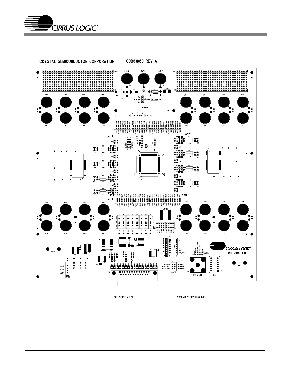
1. CDB61880 EVALUATION BOARD LAYOUT
CDB61880
Figure 1. CDB61880 Board Layout
4 DS450DB1
Page 5
2. BOARD COMPONENT DESCRIPTIONS
CDB61880
2.1 Power Connections
Power for the CDB61880 evaluation board is supplied by an external +3.3 V DC power supply. A +5
V DC power supply can also be connected to the
on-board control logic. The LED labeled “D3” will
illuminate when power is supplied to the on-board
control logic.
- Connect the +3.3 VDC power supply to the +3
V binding post and the +5 VDC power supply to
the +5 V binding post if 5 Volt logic is required
- Jumper J13 shown in Figure 2 allows all the
external logic on the evaluation board to be
connected to either +3 V or +5 V binding post.
J13
3 V
VLOGIC
5 V
On-board logic connected
to +3 V binding post
2.2 Master Clock Selection
In both Hardware and Host modes, the MCLK pin
is configured by placing a short block on one of the
positions of bed stake header J1. Figure 3 shows
the different positions of the J1 bed stake header.
HIGH
J1
Data Recovery Mode
OSCILLATOR
EXTERNAL SOURCE
GND
MCLK
HIGH
J1
On-board Oscillator
OSCILLATOR
EXTERNAL SOURCEEXTERNAL SOURCE
GND
MCLK
J13
3 V
VLOGIC
5 V
On-board logic connected
to +5 V binding post
Figure 2. On-board Logic Power Selection
- To measure the current consumption of only
the CS61880 device, place a short block on
Jumper J13 to connect the Vlogic power
supplies to the +5 V binding post. This will
isolate the CS61880 device from all the onboard logic, to allow the current measurement
to be made at the +3 V binding post.
HIGH
J1
External Clock Source
OSCILLATOR
EXTERNAL SOURCE
Figure 3. Master Clock Selections
GND
MCLK
Receivers Powered Down
HIGH
J1
OSCILLATOR
GND
MCLK
- A 2.048 MHz clock oscillator is provided on the
evaluation board for use as the on-board clock
source for all E1 modes.
- A BNC connector (labeled J16) provides the
connection for an external clock source.
DS450DB1 5
Page 6
CDB61880
2.3 Operating Mode Selection
The operating mode for the CS61880 can be selected by setting switch S15 to one of the positions
shown in Figure 4.
S15
Hardware
Serial Host
Parallel Host
MODE MODE
Selects
Hardware Mode
Figure 4. Hardware/Host Mode Selection
Hardware
Serial Host
Parallel Host
S15
Hardware
Serial Host
Parallel Host
MODE
Selects Serial
Host Mode
Selects Parallel
S15
Host Mode
2.4 Line Interface Connections
In both hardware and host modes, the receive line
signals (RTIP/RRING) are connected to the binding post labeled RXT 0-7 and RXR 0-7. The line
signals from the binding posts are coupled to the
device through two octal transformers (T1 and T9).
The receivers of the device use external resistors to
match the line impedance. These resistors are socketed for ease in changing the line impedance, for internal or external line impedance matching. During
internal line impedance matching mode, the resistor values are the same (15 Ω) for all modes of operation: E1 75 Ω and E1 120 Ω. During external
line impedance matching mode the receiver resistors need to be change to the values shown in
Table 1.
The jumpers listed in Table 2 are used to place or
bypass 1 KΩ protection resistors in series with the
receive line signals (RTIP/RRING). These resistors are used for receiver protection while in external line impedance matching mode and should not
be used during internal line impedance matching
mode. To place the 1 KΩ resistors in series with the
receive line signals, remove the short blocks from
each of the jumpers described in Table 2. To bypass the 1 KΩ resistors, place a short block on each
jumper shown in Table 2.
Table 2. Protection Resistor Selection
Jumper Description
J29 Channel 0 RRING signal
J30 Channel 0 RTIP Signal
J37 Channel 1 RTIP Signal
J38 Channel 1 RRING Signal
J46 Channel 2 RRING Signal
J47 Channel 2 RTIP Signal
J54 Channel 3 RTIP Signal
J55 Channel 3 RRING Signal
J65 Channel 4 RRING Signal
J66 Channel 4 RTIP Signal
J73 Channel 5 RTIP Signal
J74 Channel 5 RRING Signal
J81 Channel 6 RRING Signal
J82 Channel 6 RTIP Signal
J89 Channel 7 RTIP Signal
J90 Channel 7 RRING Signal
The transmit line signals (TTIP/TRING) from the
device are coupled to the line binding post (TXT 07 and TXR 0-7) through two octal transformers (T1
and T9). External protection circuitry such as diodes or chokes are recommended for protection.
For further information on line protection refer to
Application Note AN34, Secondary Line Protec-
tion for T1 and E1 Line Cards (AN34REV1 SEP
'94).
Table 1. External Impedance Resistor Values
E1 75 ΩΩΩΩ E1 120 ΩΩΩΩ
9.31
Ω
15
Ω
2.5 TXOE Selection
Jumper J23 is used to enable or High-Z all eight
transmitters in both hardware and host mode. A
shorting block on Jumper J23 places all the trans-
6 DS450DB1
Page 7
CDB61880
mitters in a high impedance state. Removing the
shorting block, enables the transmitters. See
Figure 5.
HI
TXOE
LO
J23
Enable all eight
transm itters
eight transmitters
Figure 5. Transmitter Enable Selection
HI
TXOE
LO
J23
Hi-Z all
2.6 Clock Edge Selection
In clock/data recovery mode, jumper J93 selects
the edge of RCLK and SCLK on which the
RPOS/RDATA, RNEG, and SDO data signals are
valid. When in data recovery mode, jumper J93 selects the output polarity of RPOS/RNEG. The function of J93 applies to both the Hardware and Host
mode. Figure 6 shows the settings for jumper J93
and the effect in both clock/data recovery and data
recovery only mode.
HI
CKLE
LO
Clock/Data Recovery -
RPOS/RNEG = falling
edge RCLK SDO =
rising edge SCLK
Data Recovery -
RPOS/RNEG
J93
polarity active high
can not be changed in Hardware mode. Figure 7
shows the settings for switch S10.
In Host mode, switch S10 has no effect on the
CS61880 device and should be set to the open
(middle) position.
S10
HIGH
OPEN
LOW
JASEL JASEL JASEL
Hardware Mode
- JA placed in
transmit path
OPEN
Figure 7. Jitter Attenuator Selection
S10
HIGH
LOW
Hardware Mode
- JA Disabled
S10
HIGH
OPEN
LOW
Hardware Mode
- JA placed in
receive path
2.8 Loopback Mode Selection
In Hardware mode, the Loopback modes are configured with switches S1 through S8 (0-7). Figure 8
shows the three different settings for all eight loop
back switches.
In Host mode, switches S1 through S8 must be set
to the NONE (middle) position to allow host interface control.
S1 - S8 S1 - S8 S1 - S8
HI
CKLE
LO
Clock/Data Recovery -
RPOS/RNEG = rising
edge RCLK SDO =
falling edge SCLK
Data Recovery -
RPOS/RNEG
polarity active low
J93
Figure 6. Clock Edge Selection
LloopnoneRloop
0 - 7
Hardware Mode -
Selects Remote
Loopback
LloopnoneRloop
0 - 7
Hardware Mode -
Selects no
Loopback
LloopnoneRloop
0 - 7
Hardware Mode -
Selects local
Loopback
2.7 Jitter Attenuator Selection
In Hardware mode, switch S10 (JASEL) controls
the position of the jitter attenuator for all eight
channels. The corner frequency and FIFO length
DS450DB1 7
Figure 8. Loopback Mode Selection
Page 8

CDB61880
2.9 Line Length/Impedance Selection
In Hardware mode, switch S11 (CBLSEL) is used
to set the internal or external line impedance for all
eight channels. The CBLSEL switch is also used to
select the desired pulse shape to be transmitted by
the device. Refer to the CS61880 Data Sheet for the
CBLSEL settings.
In Host mode, switch S11 has no effect on the
CS61880 device and should be set to the NC (middle) position.
2.10 Coder/Motorola/Intel Selection
In Hardware mode, switch 1 (MOT/INTL) inside
switch block S9 (S9 #1) is used to enable AMI or
HDB3 line coding. Setting switch S9 #1 to the open
(HIGH) position enables AMI coding and the
closed (low) position enables HDB3 coding.
In Host mode, switch S9 #1 is used to select either
Motorola or Intel Parallel Host mode. When set to
the open (HIGH) position Intel mode is selected
and the closed (LOW) position enables Motorola
mode. Figure 9 shows the settings for switch S9 #1
in Hardware and Parallel Host mode.
2.11 G.772 Monitoring Address Selection
In Hardware mode, the address for the G.772 NonIntrusive monitoring feature is selected by switches
3 through 7 (A4-A0) inside switch block S9. When
switches 3 through 7 inside switch block S9 are all
set to the closed “LOW” position, the G.772 NonIntrusive monitoring function is disabled. Refer to
the CS61880 Data Sheet for more address settings.
In Host mode, switches 3 through 7 inside switch
block S9 must be set to the open (high) position so
that the host interface can have control over the address signals during Parallel Host modes.
2.12 Mux/Non-Mux/BITS Clock Selection
In Hardware mode, switch 2 (MUX) inside switch
block S9 enables or disables the Channel #0 G.703
BITS Clock function. Placing switch S9 #2 in the
open “HIGH” position enables Channel #0 G.703
BITS Clock function and the closed “LOW” position disables this function.
In Host mode, switch S9 #2 (MUX) is used to select
multiplex or non-multiplex. Placing switch S9 #2
in the open “HIGH” position selects multiplex and
the closed “LOW” position selects Non-multiplex.
S9
A0
A1
A2
A3
A4
OPEN
MUX
1234 56 7
LO
MOT_\INTL
HI
Hardware Mode - Enables
AMI coding & enables
Channel 0 G.703 Bits
Clock function
8 DS450DB1
S9
S9
A0
A1
A2
A3
A4
OPEN
MUX
1234567
LO
MOT_\INTL
HI
LO
Hardware Mode - Enables
HDB3/B8ZS coding &
disables Channel 0 G.703 Bits
Enables Motorola Non-
Multiplex parallel host mode
Clock function
Figure 9. Switch S9 Settings
A0
A1
A2
A3
A4
OPEN
MUX
1234567
MOT_\INTL
HI
Parallel Host Mode -
Page 9

CDB61880
2.13 Digital Signal Connections
There are eight fourteen pin bed stake headers (labeled J4 through J11) that provide access to the
digital signals used to interface with back-end devices (framers, mappers, ASIC, etc.) and all eight
LOS signals, in both Hardware And Host mode.
Figure 10 shows the layout for one of the eight 14-
pin bed stake headers used to access the back-end
digital signals, LOS signals and the different settings for the TCLK/TNEG pins.
Bi-polar Mode
TCLK #
TCLK #
TCLK #
J1
GND
Vlogic
RCLK #
TPOS #
TNEG #
TNEG #
Vlogic
RPOS #
RNEG #
LOS #
GND
Uni-Polar Mode Active
TCLK #
TCLK #
TPOS #
TNEG #
TNEG #
TCLK #
J1
Vlogic
RCLK #
GND
Vlogic
RPOS #
RNEG #
corresponding receiver has detected a loss of signal
condition. Refer to the CS61880 Data Sheet for
LOS conditions.
2.15 JTAG Connection
A 5-pin bed stake header (J60) is provided to allow
easy access to the IEEE 1149.1 JTAG Boundary
Scan signals from the device.
2.16 Host Interface Connection
Connector J12 is used to connect the CS61880
evaluation board to the host computer, through a
standard 25 pin male to female parallel port cable.
No external µController board is required for host
interface connection. This connector is used for
LOS #
both serial and parallel interface.
3. HOST SETUP DESCRIPTION
Place the switches shown in Table 3 to the stated
configuration before setting the Mode switch (S15)
GND
to Serial or Parallel Host mode. Refer to Figure 4
on page 6 for switch S15 settings.
TAOS active when
MCLK present
RZ mode active when
MCLK absent
TCLK #
TCLK #
TPOS #
TNEG #
TNEG #
LOS #
TCLK #
Transmitters High-Z
TCLK #
TCLK #
TPOS #
TNEG #
TNEG #
TCLK #
J1
J1
GND
Vlogic
RCLK #
RPOS #
Figure 10. Digital Signal Control/Access
GND
Vlogic
RNEG #
Vlogic
RCLK #
GND
RPOS #
Vlogic
RNEG #
2.14 LOS Indicators
The two 4-LED packs D1 and D2 (labeled ALOS
0-7) represent the LOS signal status for LOS 0-7
pins. The ALOS 0-7 LEDs will illuminate when the
LOS #
GND
Table 3. Switch Settings for Host Mode
Switch Position
S1 through S8 NONE (middle)
S9 # 3 through # 7 OPEN (low)
S10 OPEN (middle)
S11 NC (middle)
S12 through S14 OPEN (middle)
- Switches #1 and #2 inside of switch block S9
are used in Parallel Host mode to select
Motorola, Intel, multiplex or Non-multiplex
modes. Switch S9 #1 and #2 are not used in
Serial Host mode.
DS450DB1 9
Page 10

CDB61880
4. HOST SOFTWARE INTERFACE
The software provided with the CDB61880 evaluation board is used to control and monitor the
CS61880 device. The program is designed to automatically read back each bit after each write. If the
bit is read back incorrectly an error will occur. The
following registers do not have the automatic read
back function:
- AWG Phase Address
- AWG Phase Data,
- Software Reset registers.
4.1 Starting the Software
There is no installation procedure associated with
the CS61880 software, simply click on the appropriate CS61880 software icon (Win95 or NT) on
the CD in the CDB61880 kit. The CS61880 software is used to evaluate the CS61880 device.
NOTE: The software can be used with Win-
Figure 11 shows the opening screen that appears
after you have launched the software.
dows
®
®
95
98®, NT® or 2000®.
,
4.2 Software Interface Buttons
The following subsections explain the functions of
buttons that are common to the register configuration screens in the CS61880 software.
4.2.1 Bit Indicator Description
The Register Bit checkbox shown in Figure 12
shows one bit, each register consists of eight bits (0
through 7). The grayed-out bits in some registers
are bits that can not be accessed. Figure 12 shows a
bit with a check mark and without a check mark. A
check represents a “1” and no check mark equals a
“0”.
Figure 12. Register Bit Box
4.3 Set All Button Description
The Set All button shown in Figure 13 is used to set
all the bits in the corresponding register to 1s. This
button is placed to the left of each register that has
write access.
Figure 13. Set All Button
Figure 11. CS61884 Software Opening Screen
10 DS450DB1
Page 11

4.3.1 Clear All Button Description
The CLR All Button shown Figure 14 is used to set
all the bits in the corresponding register to 0s. This
button is placed to the left of each register that has
write access.
Figure 14. Clear All Button
4.3.2 Write All Button Description
CDB61880
Figure 16. Read All Button
4.4 Write Button Description
The Write button shown in Figure 17 writes the
bits of the corresponding register. This button is located to the right of every register that allows write
access.
The Write All button shown in Figure 15 writes
every bit of every register on the current register
screen. This button is located in the bottom right
corner of each register screen.
Figure 15. Write All Button
4.3.3 Read All Button Description
The Read All button shown in Figure 16 reads every bit of every register on the current register
screen. This button is located in the bottom left corner of each register screen.
Figure 17. Write Button
4.5 Read Button Description
The Read button shown in Figure 18 reads the bits
of the corresponding register. This button is located
to the right of every register.
Figure 18. Read Button
4.6 Program Exit Function
To exit any of the register screens simple press the
X in the top right hand corner of each screen. This
DS450DB1 11
Page 12

5. CS61880 CONFIGURATION SCREENS
CDB61880
5.1 Choose Parallel Port Settings
The opening screen shown before in Figure 11 and
now in Figure 19 is used for the following configuration activities:
- Select the Parallel Port mode of operation
- Select the parallel port address
Click the appropriate radio button to choose the operational modes you wish to use.
Important Notes:
1. If the mode of operation does not match the
mode switches on the evaluation board, an
error will occur.
2. If the parallel port address does not match
the address of the control parallel port,
access to the register bits will not be
permitted.
5.2 Access and Configure the Read / Write Registers
You also use the opening screen to access the
tabbed configuration screens for the Read / Write
Registers.
5.2.1 Access Configuration Screens
Click on the Read/ Write Registers button on the
opening screen to start configuring these registers.
5.2.2 Select Register to Configure
When the next screen appears, select the desired
register screen by clicking on one of the TABs labeled Loopback/Bits Clk, LOS/AIS/DFM,
XMIT, AWG, or GCR at the top of the
Read/Write Register screen.
Figure 19. Opening Screen for Port and Address Selection Screen
12 DS450DB1
Page 13

CDB61880
5.3 Loopback /Bits Clock Screen
The Loopback /Bits Clock Register tabbed screen
shown in Figure 20 allows access to the following
registers:
- Remote loop back
- Analog loop back
- Digital Loopback
- G.703 Bits Clock
Figure 20. Loopback/G.703 Bits Clock Selection Screen
DS450DB1 13
Page 14

CDB61880
5.4 LOS/AIS/DFM/JA Register Screen
The LOS/AIS/DFM/JA Register tabbed screen
shown in Figure 21 allows access to the following
registers:
- LOS Status
- LOS Interrupt Enable
- LOS Interrupt Status
- LOS/AIS Mode Enable
- DFM Status
- DFM interrupt Status
- DFM Interrupt Enable
- AIS Status
- AIS Interrupt Enable
- AIS Interrupt Status
- JA Error Interrupt Enable
- JA Error Interrupt Status.
Figure 21. LOS/AIS/DFM/JA ERR Status/Enable Selection Screen
14 DS450DB1
Page 15

CDB61880
5.5 Transmitter Register Screen
The Transmitter Register screen shown in
Figure 22 consists of the following registers:
- Automatic TAOS
- TAOS Enable
- Performance Monitor
- Line Length Channel ID
- Line Length Data
- Output Disable.
NOTE: Some indictor boxes (bits) in the Performance
Monitor, Line Length Channel ID, and Line
Length Data registers are grayed out, this
means that these bits can not be accessed.
Figure 22. Transmitter Register Screen
DS450DB1 15
Page 16

CDB61880
5.6 AWG Register Screen
The AWG Register screen shown in Figure 23 allows access to the following AWG registers:
- AWG Broadcast
- AWG Enable
- AWG Overflow Interrupt Enable
- AWG Overflow Interrupt Status
- AWG Phase Address
- AWG Phase Data.
The AWG Phase Address Register is broken up
into two easy-to-use data input boxes: the Chan
Address (i.e., channel address) and the Sample
Address. For example, to access the AWG func-
tion for channel 5, write 05 into the Chan Address
input box. This is the same for every channel. The
Chan Address, Sample Address, and Phase Data
input boxes use the values discussed in the AWG
section of the CS61880 Data Sheet.
Figure 23. AWG Registers Screen
16 DS450DB1
Page 17

CDB61880
5.7 Global Control Register Screen
Figure 24 shows the Global Control Register
(GCR) screen, The GCR register screen consists of
the following registers:
- Software reset
- ID registers.
Each bit in the Global Control Register can be access by writing directly to the bit in the Global Control Register on the top of this screen or by
changing the radio buttons in one of the following
windows:
- Jitter Attenuator
- JA FIFO Length
- AWG Auto Increment
- Raisen
- Coden
- Jitter Corner Freq.
The variables listed above change the corresponding bit in the Global Control Register. The Software Reset Register is a write only register and will
clear after the write. The ID Register is a read only
register.
Figure 24. Global Control Screen
DS450DB1 17
Page 18

CDB61880
6. BOARD CONFIGURATIONS
tion board to operate in E1 75 Ω Hardware, Serial
Host and Parallel Host operational modes. Before
6.1 E1 75 ΩΩΩΩ Mode Setup
Table 4 shows the position of the different switches
selecting Host mode, the switches in Table 4 in
bold should be set to the position stated.
and jumpers used to set up the CDB61880 evalua-
Table 4. E1 75 ΩΩΩΩ Operational Mode Switch/Jumper Position
Switches/Jumpers Hardware Serial Host (Note 3) Parallel Host (Note 3)
S15 (MODE) HARDWARE SERIAL HOST PARALLEL HOST
S1 (0) LOOP FUNCTION NONE NONE
S2 (1) LOOP FUNCTION NONE NONE
S3 (2) LOOP FUNCTION NONE NONE
S4 (3) LOOP FUNCTION NONE NONE
S5 (4) LOOP FUNCTION NONE NONE
S6 (5) LOOP FUNCTION NONE NONE
S7 (6) LOOP FUNCTION NONE NONE
S8 (7) LOOP FUNCTION NONE NONE
S9 #1 (MOT_\INTL) HIGH HIGH MOTOROLA/INTEL
S9 #2 (MUX) LOW (Note 4) HIGH MUX/NON-MUX
S9 #3 (A4) LOW (Note 5) HIGH HIGH
S9 #4 (A3) LOW (Note 5) HIGH HIGH
S9 #5 (A2) LOW (Note 5) HIGH HIGH
S9 #6 (A1) LOW (Note 5) HIGH HIGH
S9 #7 (A0) LOW (Note 5) HIGH HIGH
S10 (JASEL) ANY POSITION OPEN OPEN
S11 (CBLSEL) HIGH (Note 6) NC NC
J13 (VLOGIC) 3 V 3 V 3 V
J1 (MCLK) OSCILLATOR OSCILLATOR OSCILLATOR
J93 (CLKE) OPEN OPEN OPEN
J23 (TXOE) OPEN OPEN OPEN
3. Connect a standard 25-pin male to female parallel port cable to connector J12 and the control PC.
4. Set “HIGH” to enable BITS Clock Recovery function for only Channel #0 in Hardware Mode.
5. Other settings may be used to enter G.772 Non-Intrusive Monitoring in Hardware Mode. Refer to the
CS61880 Data Sheet for other settings.
6. Set “LOW” to disable receiver Internal line impedance matching function. The external resistors for all
eight receivers must be changed to 9.31 Ω to properly match the input line impedance.
18 DS450DB1
Page 19

CDB61880
6.2 E1 120 ΩΩΩΩ Mode Setup
Table 5 shows the position of the different switches
and jumpers used to set up the CDB61880 evalua-
Host and Parallel Host operational modes. Before
selecting Host mode, the switches in Table 5 in
bold should be set to the position stated.
tion board to operate in E1 120 Ω Hardware, Serial
Table 5. E1 120 ΩΩΩΩ Operational Mode Switch/Jumper Position
Switches/Jumpers Hardware Serial Host (Note 3) Parallel Host (Note 3)
S15 (MODE) HARDWARE SERIAL HOST PARALLEL HOST
S1 (0) LOOP FUNCTION NONE NONE
S2 (1) LOOP FUNCTION NONE NONE
S3 (2) LOOP FUNCTION NONE NONE
S4 (3) LOOP FUNCTION NONE NONE
S5 (4) LOOP FUNCTION NONE NONE
S6 (5) LOOP FUNCTION NONE NONE
S7 (6) LOOP FUNCTION NONE NONE
S8 (7) LOOP FUNCTION NONE NONE
S9 #1 (MOT_\INTL) HIGH OPEN MOTOROLA/INTEL
S9 #2 (MUX) LOW (Note 4) OPEN MUX/NON-MUX
S9 #3 (A4) LOW (Note 5) OPEN OPEN
S9 #4 (A3) LOW (Note 5) OPEN OPEN
S9 #5 (A2) LOW (Note 5) OPEN OPEN
S9 #6 (A1) LOW (Note 5) OPEN OPEN
S9 #7 (A0) LOW (Note 5) OPEN OPEN
S10 (JASEL) ANY POSITION OPEN OPEN
S11 (CBLSEL) NC (Note 7) NC NC
J13 (VLOGIC) 3 V 3 V 3 V
J1 (MCLK) OSCILLATOR OSCILLATOR OSCILLATOR
J93 (CLKE) OPEN OPEN OPEN
J23 (TXOE) OPEN OPEN OPEN
7. Set to “NC” to disable receiver Internal line impedance matching function. The external resistors for all
eight receivers must be changed to 15 Ω to properly match the input line impedance.
DS450DB1 19
Page 20

CDB61880
7. EVALUATION HINTS
- Pin #1 of the socket is indicated by an arrow
with U1 below it.
- A short in the desired position must be placed
on Jumper J13 to connect the CS61880 to one
of the power supply binding post. LED D3 will
illuminate when jumper J13 is connected to a
power supply.
- Before selecting any Host mode place the
CBLSEL, LOOP, ADDRESS and JASEL
switches in the open or none position.
- When using the CS61880 device in Internal
Match Impedance mode, be sure that the 1 KΩ
resistors are not in series with the receivers.
20 DS450DB1
Page 21

• Notes •
Page 22

 Loading...