

Page 1
FEATURES
■Socketed CS61584A Dual Line Interface
■All Required Components for CS61584A
Evaluation
■Locations to Evaluate Protection Circuitry
■LED Status Indications for Alarm Conditions
■Support for Hardware and Host Modes
ORDERING INFORMATION:
CDB61584A
CDB61584A
Product Databook
Dual Line
Interfac e U n i t
DESCRIPTION
The evaluation board includes a socketed CS61584A
dual line interface device and all support components
necessary for evaluation. The board is powered by an
external +5 Volt supply.
The board may be configured for 100Ω twisted-pair T1,
75Ω coax E1, or 120Ω twisted-pair E1 operation. Binding posts and bantam jacks are provided for line
interface connections. Several BNC connectors provide
clock and data I/O at the system interface. Reference
timing may be derived from a quartz crystal, crystal oscillator, or an external reference clock. Four LED
indicators monitor device alarm conditions.
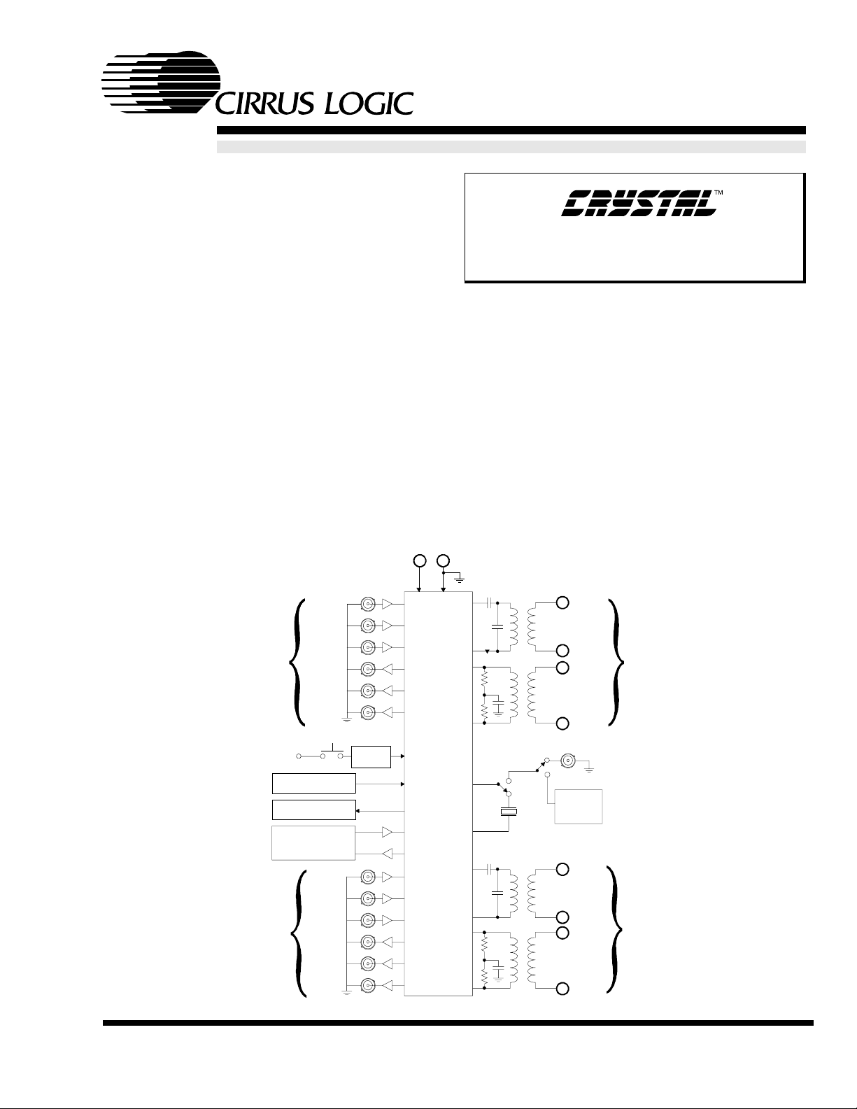
5V+0V
CHANNEL1
CHANNEL2
TCLK1
TPOS1
(TDATA1)
TNEG1
RCLK1
RPOS1
(RDATA1)
RNEG1
(BPV1)
V+
HardwareControl
andModeCircuit
LEDStatus
Indicators
SerialInterface
ControlCircuit
TCLK2
TPOS2
(TDATA2)
TNEG2
RCLK2
RPOS2
(RDATA2)
RNEG2
(BPV2)
RESET
CIRCUIT
CS61584A
XTL
TTIP1
TRING1
RTIP1
RRING1
Oscillator
Circuit
TTIP2
TRING2
RTIP2
RRING2
CHANNEL1
REFCLK
CHANNEL2
DS261DB2 MAR ‘98
Copyright Cirrus Logic, I nc. 1998
(All Rights Reserv ed)
Page 2

CDB61584A
Dual Line Interface Unit
POWER SUPPLY
As shown on the evaluation board schematic in
Figures 1-5, power is supplied to the board from an
external +5 Volt supply connected to the two binding posts labeled V+ and GND. Zener diode Z1
protects the components on the board from reversed supply connections a nd over-voltage da mage. Capacitor C16 provides power supply
decoupling and ferrite bead L1 helps isolate the
CS61584A and buffe r supplies. Both sides of the
evaluation board contain extensive areas of ground
plane to insure optimum perfo rm ance.
Capacitors C3, C5-C8, C13, C18, and C38 provide
power supply decoup ling for the CS61584A. The
BGREF pin is pulled down through resistor R10 to
provide an in ternal current referenc e. The buffers
are decoup led usi ng capa citors C 9, C15, and C1 9.
Ferrite bea ds L2 -L4 he lp re duce th e pow er sup ply
noise that i s c oupl ed from the buffers to the p ower
supply.
BOARD CONFIGURATION
Slide switch SW6 selects hardware or host mode
operation. Hardware mode is selected when switch
SW6 is in the "HW" position and sets the MODE
pin of the CS61584A to a logic 0. Host mode is selected wh en switch SW6 is in the "SW" pos ition
and sets the MODE pin of the CS61584A to a
logic 1.
Hardware Mode
In Hardware m ode operat ion, the evaluation board
is configured using DIP switches SW2, SW 3, and
SW4. In this mode, t he switc he s est ab li s h the digital contro l inputs for bo th line interfa ce channels.
Closing a DIP switch towards the label sets the
CS61584A control pi n of the same name to a logic
1. The host pr ocessor interfac e J26 should not be
used in the Hardware mo de.
The CDB61584A switches and functions are listed
below:
- TAOS1, TAOS2: transmit all ones;
- LLOOP: local loopback of both channe ls;
- RLOOP1,2: remote loopback 1,2;
- PD1, PD2: power down;
- ATTEN0, ATTEN1: jitter attenuator selection;
- CLKE: RCLK edge polarity;
- 1XCLK: clock frequency selection;
- CONx1, CONx2: line configuration settings.
All switch inputs are pulled-down using resistor
networks RP2-RP5.
The LOS1 and LOS2 LED indicators illuminate
when the line interface receiver has detected a lo s s
of signal. Headers J7 and J13 must be jumpered in
the "TNEG" position to provide connectivity to the
BNC input in Hardware mode.
Host Mode
In Host mode o perat io n, t he e valua tion bo ard sup ports serial-po rt operation o ver interface port J26
using the printer port of a host PC equipped with
the enclosed software. The evaluation board is connected to the host PC using the ribbon cable provided. The SW2 switch position labeled "ATTEN0"
must be open to set th e P/S pin of the CS6 1584A to
a logic 0 and en able serial-por t ope ration.
An external m icroprocessor may also in terface to
the evaluation board for the purposes of system
software development. The CS61584A interrupt
pin is connecte d to pin 23 of interf ace port J26 to
facilitate software developme nt. The SW2 switch
position labele d "CL KE/ IPOL" es tabl ishes the po larity of the interrupt pin. If an active low interrupt
is selected (IPOL low), the interrupt pin must be
pulled-up through resistor R55 by placing a jumper
on header J24. The SW2 switch position labeled
"RLOOP1" must be in the open position for proper
operation of the interrupt.
The LOS1 and LOS2 LED indicators illuminate
when the line interface receiver has detected a lo s s
of signal. If coder mode is enabled in the
CS61584A registe r set , the A IS alarm cond itio n is
52 DS261DB2
Page 3

CDB61584A
Dual Line Interface Unit
provided when headers J7 and J13 are jumpered in
the "AIS" position. The AIS1 and AIS2 LED indicators illuminate when the line interface receiver
has detected the all-ones rec eive input sign al. Resistors R26 and R 27 pull -dow n the TNE G(1,2) in puts when coder mode is disabled b ut headers J7
and J13 are jumpered i n the " A IS " position.
Further details concerning Host mode operation are
described in t he "readme.txt" file on the enclosed
disk.
Manual Reset
A momentary contact switch SW1 provides a manual reset by forcing the RESET pin of the
CS61584A to a l ogic 1 . Alth ough th e t ransm it and
receive circuitry are continuously calibrated, the
reset can b e used to in it iali ze t he cont rol l ogic and
clear the register set. Both channels are powered up
after exit in g r eset.
TRANSMIT CIRCUIT
The transmit clock and data signals are supplied on
BNC inputs labeled TCLK(1,2), TPOS(1,2), and
TNEG(1,2). In Hardware and Host mode (with
coder mode disabled), data is supplied on the
TPOS(1,2) and TN EG( 1,2) BNC inpu ts in RZ for mat. In Host mode with code r mode enabled , data
is supplied on the TDATA(1,2) BNC input in NRZ
format and the TNEG(1,2) BNC input may be used
to indicate the AIS alarm condition as described in
the Host Mode section.
The transmitter output is transformer coupled to the
line interfa ce through 1:1.15 step-up transforme rs
T1 and T4. The signal is available at either the
TTIP(1,2) and TRING(1,2) binding posts or the
TX(1,2) bant am jacks.
Capacitors C2 and C11 prevent output stage imbalances from prod ucing a DC cu rrent that m ay saturate the transformer and result in an output level
offset. Capacitors C1 and C12 p rovide tran smitter
return loss and are socketed so the value may be
changed according to the application. A 220 pF ca-
pacitor is required for 100Ω twisted-pair T1 or
120Ω twisted-pa ir E1 applications. A 470 pF capacitor is requi red for 75Ω coax E1 applic ations.
These capacitors are included with the evaluation
board.
Optional diode locations D6-D9 and D10-D13 and
optional resistor locations R8-R9 and R18-R19
provide test locat ions to evaluate transm it line interface prote ction circuit ry.
RECEIVE CIRCUIT
The rece ive signal is inp ut at eit her the RTIP(1,2 )
and RRING(1,2) binding posts or the RX(1,2) bantam jack s. The receive signal is tra nsformer coupled to the CS61584A through 1:1.15 step-down
transformers T2 and T3.
The receive line is terminated by resistors R3-R4
and R14-R15 to pro vide impedance matching and
receiver return l oss. Th ey are socket ed so the values may be cha nged according to the applicati on.
The evaluati on board is supplied from the factory
with 38.3Ω resistors for terminating 100Ω twistedpair T1 lines, 45.3Ω resistors for terminating 120Ω
twisted-pair E1 lines, and 28.7Ω resistors for terminating 75Ω coaxial E1 lines. Capacitors C4 and
C10 provide a differential input voltage reference.
Optional resistor loc ations R1 -R2, R12-R 13, R16R17, and R24 -R25 provi de t est loc ations t o eva luate receiv e l ine interface protection circuitry.
The recov ere d clo ck and d at a sign al s ar e a vail able
on BNC outputs labeled RCLK(1,2), RPOS(1,2),
and RNEG(1,2). In Hardware and Host mode (with
coder mode disabled), data is available on the
RPOS(1,2) and RNEG(1,2) BNC outputs in RZ
format. In Host mode with coder mode enabled,
data is ava ilable on the RDATA(1,2) BNC output
in NRZ format an d bipolar viol ations are re ported
on BPV(1,2).
DS261DB2 53
Page 4

CDB61584A
Dual Line Interface Unit
REFERENCE CLOCK
The CDB61584A requires a T1 or E1 reference
clock for op eration. Th is clock may operate at e ither a 1-X rate (1.544 MHz or 2.048 MHz) or an 8X rate (12.352 MHz or 16.384 MH z) and can be
supplied by eithe r a qua rtz crys tal, cryst al osci llator, or exte rnal referenc e. The eva luation boar d is
supplied from the fa ctory wi th two crystal oscilla tors for T1 and E1 operation.
Quartz Crystal
A quartz cry sta l m ay be inse rt ed at s oc ket Y 1. Be cause the c rystal operate s at a n 8-X ra te, t he S W2
switch position l abel ed "1XC LK " must be op en to
set the 1XCL K pin of the CS61584A to a logic 0
and enable 8-X clock ope ration.
Crystal Oscillator
A crystal oscillator may be inserted at socket U4 in
the orient atio n indi cated by the s ilksc reen . Hea der
J14 must be jumpered in the "OSC" position to provide connectivity to the REFCLK pin of the
CS61584A. The SW2 switch position labeled
"1XCLK" must be open (logic 0) for 8-X clock operation or closed (logic 1) for 1-X clock operation.
External Reference
An external reference may be provided at the REFCLK BNC input . Head er J1 4 must be ju mper ed in
the "REFCL K" p os ition t o p rov ide c onnec ti vity to
the REFCLK pin of the CS61584A. The SW2
switch position labeled "1XCLK" must be open
(logic 0) for 8-X clock operation or closed (logic 1)
for 1-X clock operation.
BUFFERING
Buffers U2, U3, and U6 provide additional drive
capability for the BNC and Host mode connections.
The buffer outputs are filtered with an RC network
to reduce the transients caused by buffer switching.
JTAG ACCESS
The CS61584A im plements JTAG bound ary scan
to support board-level testing. Interface port J56
provides access to the four JTAG pins on the
CS61584A. The J-TMS pin of the CS61584A is
pulled-down by resistor R28 to disable boundary
scan unles s the pin i s externa lly pull ed high us ing
the interfa ce port.
TRANSFORMER SELECTION
The evaluati on board is supplied from the factory
with Pulse Engi ne ering PE-65388 transformer s installed at locations T1-T4. They are socketed to
permit the evaluation of other transformers.
LINE PROTECTION EVALUATION
Several optional resistor and diode locations on the
transmit and receive line interface allow for the installation and evaluation of various types of protection circuitr y. Each locatio n is drilled wit h 60 mil
vias to permit the installation of sockets. These
sockets can be obtained from McKenzie at (510)
651-2700 by requesting part #PPC-SIP-1X32620C and are identical to the socket type installed
at the re c eive resist or locations on t he board. They
allow the line protection circuitry to be easily
changed d uring testi ng. Note that the traces forming shorts between the socket locations on the line
interface may need to be cut prior to the installation
of protectio n circuitry.
PROTOTYPING AREA
Four prototyping areas with power supply and
ground connec t ions are provided on the evaluation
board. These areas c an be used to de velop and test
a variety of additional circ uits such as fram er devices, system synchronizer PLLs, or specialized interface log ic .
54 DS261DB2
Page 5

CDB61584A
Dual Line Interface Unit
EVALUATION HINTS
1) The orientation of pin 1 for the CS61584A is labeled "1" on the left sid e of t he soc ket U7.
2) A jumper must not be placed on header J10
when using the CDB 61584A.
3) Component locations R3-R4, R14-R15, C1,
and C12 must have th e cor rec t val ues insta lled
according t o the applica tion. All th e necess ary
components are included with the evaluation
board.
4) Closing a DIP switch on SW2, SW3, and SW4
towards the label sets the CS61584A control
pin of the same nam e to logic 1.
5) When performing a manual loopback of the recovered signal to the transmit signal at the BNC
connectors, the recovered data must be valid on
the falling edge of RCL K to prope rly latch the
data in the transmit direction. To accomplish
this, the S W2 switc h posit ion labe led " CLKE "
must be closed (logic 1) during Hardware mode
operation or the CLKE bit in the Control A register must be set to a 1 during Host mode oper ation.
6) Jump ers can be place d on head ers J9 an d J12 to
provide a ground reference on TRING for 75 Ω
coax E1 applications.
7) Properly terminate TTIP/TRING when evaluating the transmit output pulse shape. For more
information concerning pulse shape evaluation,
refer to the Crystal application note entitled
"Measurement and Evaluation of Pulse Shapes
in T1/E1 Transmiss io n Syst ems."
DS261DB2 55
Page 6

RCLK1
RPOS1
(RDATA1)
RNEG1
(BPV1)
(TDATA1)
TTIP1
TRING1
RTIP1
RRING1
TCLK1
TPOS
TNEG
J31
J32
J33
J34
J1
J2
J3
J4
J5
J6
AIS1
LOS1
51.1
R30
51.1
R31
51.1
D1
LED
D2
LED
R
R
R29
T
T
J8A
J8B
R6
470
R7
470
3
5
7
4
6
8
Q1
Q2
1
4
6
9
U2
C26
100pF
U2
C27
100pF
U2
C28
100pF
U2
100pF
U2
C30
100pF
U2
100pF
VA+
3
3
C29
C31
1
1
17
15
13
16
14
12
VA+
J9
2
2
R24
R25
R8
R9
R5
51.1
1
4
3
J7
R26
47K
T1
1
3
5
1.15:1
PE -65388
T2
1
3
5
1.15:1
PE -65388
CDB61584A
Dual Line Interface Unit
VA+
L4
VCC
ENA
1
10
11
12
13
14
15
16
17
18
19
20
21
22
23
24
25
26
20
U2
10
RCLK1
RPOS1
RNEG1
TCLK1
TPOS1
TNEG1
LOS1
J-TDO
DGND2
J-TDI
TTIP1
TV+1
TGND1
TRING1
PD1
ATTEN0
N/C-1
19
GND
U7
CS61584A
CHANNEL 1
RTIP1
RRING1
27
28
ENA
TV+1
C9
.1µF
R38
R39
2
VD+
51.1
51.1
J-TDO
J-TDI
C3
.1µF
PD1
ATTEN0
VD+
D10
2
D11
D13
C1
C2
.47µF
R1
R2
R3
VD+
6
D12
2
6
R4
C4
.47µF
Notes: Components R3, R4, and C1 are socketed to permit value changes
to the application.
Component locations R1, R2, R8, R9, R24, R25, and D10-D13 provide
areas for evaluating protection circuitry.
Figure 1. Channel 1 Circuitry
56 DS261DB2
Page 7

CDB61584A
Dual Line Interface Unit
VA+
ENA
ENA
U7
CS61584A
CHANNEL 2
TV+1
C38
22
F
µ
L2
19
GND
RRING2
41
VCC
1
U3
RCLK2
RPOS2
RNEG2
TCLK2
TPOS2
TNEG2
CON32
J-TCK
J-TMS
TGND2
TRING2
RTIP2
42
20
10
N/C-3
LOS2
TTIP2
TV+2
PD2
CLKE
N/C-2
43
J16
U3
U3
100pF
U3
Q4
6
9
1
4
VA+
3
1
R21
470
J11B
J11A
R41
RCLK2
51.1
J17
R42
51.1
R43
51.1
6
4
2
Q3
R20
D3
LED
470
J18
J19
J20
J21
AIS2
RPOS2
(RDATA2)
RNEG2
(BPV2)
TCLK2
TPOS2
(TDATA2)
TNEG2
LOS2
D4
LED
J27
TTIP2
T
R
J28
J29
T
R
J30
TRING2
RTIP2
RRING2
U3
U3
U3
100pF
2
9
C32
100pF
7
C33
100pF
5
C34
100pF
14
C35
16
C36
18
C37
100pF
2
VA+
3
1
11
13
C15
.1µF
60
59
58
57
56
55
54
53
52
51
50
49
48
47
46
45
44
R50
R51
10K
CON32
J-TCK
J-TMS
R28
PD2
CLKE
C13
.1µF
51.1
51.1
VD+
1
3
J13
R27
47K
15
R22
2
51.1
4
VD+
.47µF
C12
C11
R12
R13
R14
D7
D9
C10
D6
VD+
D8
R15
T4
261
3
5
1:1.15
PE-65388
T3
261
3
5
1:1.15
PE-65388
R18
R19
J12
R16
R17
.47µF
Notes: Components R14, R15, and C12 are socketed to permit value changes according
to the application.
Component locations R12, R13, R16-R19, and D6-D9 provide areas for evaluating
protection circuitry.
Figure 2. Channel 2 Circuitry
DS261DB2 57
Page 8

CDB61584A
Dual Line Interface Unit
VD+
SW2
124
223
322
421
520
619PD1
718PD2
817ATTEN0
916ATTEN1
10 15
11 14
12 13
J24
TAOS2
TAOS1
LLOOP
RLOOP2
RLOOP1
CLKE/IPOL
1XCLK
765432 876543
8
RP4
47k
SCLK
2
C20
R57
51.1
25
23
21
19
17
15
13
11
9
7
5
3
1
6
U6
14
J26
26
24
22
20
18
16
14
12
10
8
6
4
2
PD1
PD2
ATTEN0
CLKE/IPOL
1XCLK
2
U6
18
C23
9
SD0
INT
VD+
R55
3.92k
CS
SD1
11
RP5
47k
GNDGND
100pF
100
pF
R58
8
R40
51.1
4
U6
16
51.1
765
100 pF
U6
11
C24
100pF
4
C25
9
9
5
R
51.1
3
GND
2
51.1
.01
C18
1
R56
100 pF
7
C39
U6
GND
13
RP2
VD+
µ
F
68676665646362
1
47k
23456
CON32
61
J-TD0
J-TD1
J-TMS
T-TCK
RP3
1
3
5
7
23456
J56
CON01
CON11
CON21
CON31
47k
1
2
4
6
8
SW3
SW4
VD+
81
72
63
54
81CON02
72CON12
63CON22
54CON32
N/C-4
ATTEN1
TAOS1
LLOOP
RLOOP1
RLOOP2
CONTROL CIRCUITRY
TAOS2
CON01
DGND1
U7
CS61584A
DV+
CON02
CON11
CON12
CON21
CON22
DGND3
CON31
Figure 3. Control Circuitry
58 DS261DB2
Page 9

CDB61584A
Dual Line Interface Unit
29
CS61584A
TIMING CIRCUITRY
RV+1
RGND1
MODE
BGREF
30
313233
U7
AGND
AV+
343536
RESET
REFCLK
XTALOUT
1XCLK
RGND2
RV+2
38
37
39
40
SW6
R23
VD+
VD+
C14
.1µF
.1µF
47K
VA+
C5
C6
C7
VCC
GND
SW1
R10
.1µF
1.0
1
2
VD+
U4
µ
4.99k
F
VD+
R11
J14
8
Y1
10K
42
13
1XCLK
C8
.1µF
VD+
J 10
(must not
be jumped)
REFCLK
J15
Figure 4. Timing Circuitry
DS261DB2 59
Page 10

CDB61584A
Dual Line Interface Unit
J22
VA+
V+
C16
47µF
Z1
L1
Prototyping Area
GND
J23
VD+
VD+
Figure 5. Common Circuitry
60 DS261DB2
Page 11

• Notes •
Page 12

Preliminary product information describes products which are in production, but for which full characterization data is not yet available. Cirrus
Logic, Inc. has made best efforts to ensure that the information contained in this document is accurate and reliable. However, the information
is subject to change without notice and is provided “AS IS” without warranty of any kind (express or implied). No responsibility is assumed by
Cirrus Logic, Inc. for the use of this infor ma tio n, nor for infr ingem ents of pa tent s or oth er right s of third pa rtie s. Thi s d o cument is the property of
Cirrus Logic, Inc. and implies no license under patents, copyrights, trademarks, or trade secrets. No part of this publication may be copied,
reproduced, stored in a retrieval system, or transmitted, in any form or by any means (electronic, mechanical, photographic, or otherwise). Furthermore, no part of thi s pub lication m ay be u sed a s a basi s for ma nufactur e or sal e of any i tems with out the prior w ritten c onsen t of Cirr us Logic,
Inc. The names of products of Ci rrus Logi c, Inc. or other vend ors and s uppliers a ppear ing in this doc ument m ay be trade marks o r service marks
of their respec tive own er s whi ch may b e r egi ster ed in som e j uri sd ictio ns. A lis t of C irr us Logic, Inc. tradem ark s and servi ce marks can be fou nd
at http://www.cirrus.com.
 Loading...