

Page 1
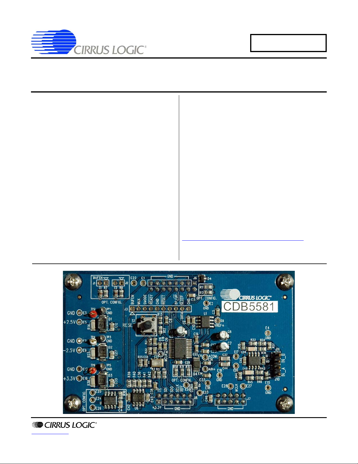
CDB5581
200 kSps, 16-bit, High-throughput
Evaluation Board
Features
Analog Input Channel to the CS5581 ADC
Pre-configured to require a minimum number of external
connections to your data acquisition system.
All functionality accessible through the connector interface
and board-level options.
On-board 4.096 V Reference
Pre-configured for Master mode SPI™ communication to a
data capture system.
ΔΣ
ADC
General Description
The CDB5581 is a versatile tool designed for evaluating the functionality and performance of the CS5581 ADC (Analog-to-Digital
Converter). The SPI serial port on the CDB5581 evaluation board
is configured in Master mode and will start transmitting data after
power-up upon reset. This evaluation board is designed to connect
to your data capture system or will interface to the CapturePlus II
data acquisition system available from Cirrus Logic.
The CS5581 delta-sigma ADC produces fully settled conversions to
full specified accuracy at 200 kSps. This ability to produce fully settled conversions for every sample makes it suitable for converting
multiplexed input signals. To help evaluate this feature, the CDB5581
includes two sing le-ended analog inputs multiplexed into the
CS5581. The multiplexer can be switched at the CS5581 ADC sample speed and the ADC will produce fully settled conversion data for
each input channel.
All evaluation board functionality for evaluating the CS5581 ADC is
accessed through the connector interface and board-level options.
Schematics in PADS™ PowerLogic™ format are available for
download at:
http://www.cirrus.com/en/products/pro/detail/P1120.html
ORDERING INFORMATION
CDB5581 Evaluation Board
.
www.cirrus.com
Copyright Cirrus Logic, Inc. 2009
(All Rights Reserved)
OCT ‘09
DS796DB3
Page 2

CDB5581
TABLE OF CONTENTS
1. INTRODUCTION ....................................................................................................................... 3
1.1 Overview ............................................................................................................................ 4
2. QUICK START .......................................................................................................................... 5
3. HARDWARE DESCRIPTION ...................................................................................................6
3.1 Absolute Maximum Ratings ............................................................................................... 6
3.2 Power Supply ..................................................................................................................... 6
3.3 Analog Section ................................................................................................................... 6
3.3.1 Analog Input Buffers .............................................................................................. 6
3.3.2 Multiplexer ............................................................................................................. 7
3.3.3 ADC Reset ............................................................................................................ 7
3.3.4 Voltage Reference ................................................................................................ 7
3.3.5 ADC Reference Frequency ................................................................................... 7
3.4 Digital Section .................................................................................................................... 8
3.4.1 Hardware Configuration ........................................................................................ 8
3.4.2 SPI™ Serial Port Communications ....................................................................... 8
APPENDIX A. MAXIMIZING THE PERFORMANCE OF THE CS5581 ........................................ 9
A.1 PCB Layout Considerations .............................................................................................. 9
A.2 Hardware Considerations .................................................................................................. 9
APPENDIX B. BILL OF MATERIALS ........................................................................................ 10
APPENDIX C. SCHEMATICS ..................................................................................................... 11
APPENDIX D. LAYER PLOTS ................................................................................................... 16
APPENDIX E. CALIBRATION FUNCTION ................................................................................. 25
APPENDIX E. REVISION HISTORY ..........................................................................................26
LIST OF FIGURES
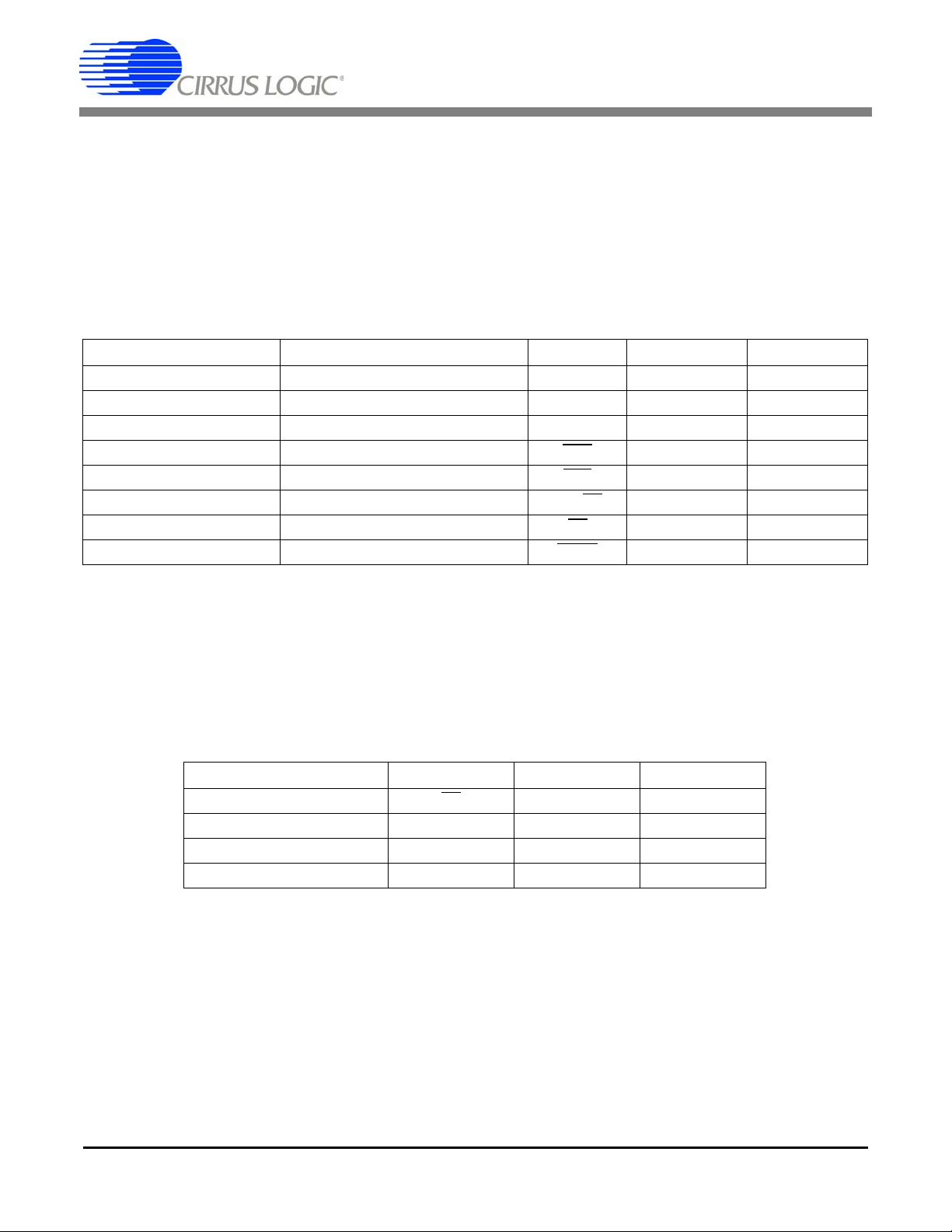
Figure 1. CDB5581 Block Diagram .................................................................................................4
Figure 2. CDB5581 Board Layout ................................................................................................... 5
Figure 3. Schematic - Block Diagram............................................................................................ 11
Figure 4. Schematic - Power Supplies .......................................................................................... 12
Figure 5. Schematic - Input Buffers and Multiplexer ..................................................................... 13
Figure 6. Schematic - CS5581 ...................................................................................................... 14
Figure 7. Schematic - Configuration & Misc. ................................................................................. 15
Figure 8. Top Silkscreen ............................................................................................................... 16
Figure 9. Top Solder Mask ............................................................................................................ 17
Figure 10. Top Routing.................................................................................................................. 18
Figure 11. Ground Plane ............................................................................................................... 19
Figure 12. Power Plane................................................................................................................. 20
Figure 13. Bottom Solder Mask..................................................................................................... 21
Figure 14. Bottom Silkscreen ........................................................................................................ 22
Figure 15. Top Solder Paste Mask................................................................................................23
Figure 16. Bottom Routing ............................................................................................................ 24
LIST OF TABLES
Table 1. Power Supply Connections ...............................................................................................6
Table 2. Analog Input Connections ................................................................................................. 6
Table 3. Analog Input Channel Selection ........................................................................................ 7
Table 4. Hardware Configuration Signals........................................................................................ 8
Table 5. Serial Interface Connections ............................................................................................. 8
2 DS796DB3
Page 3

CDB5581
1. INTRODUCTION
The CDB5581 evaluation board is a platform for evaluating the CS5581 ADC performance. The evaluation board is designed to connect to the SPI serial port of a processor or data capture system or will interface directly to the CapturePlus II data acquisition system available from Cirrus Logic. The CapturePlus II
data acquisition system is a powerful integrated hardware/software tool designed to fully exercise the
CDB5581 and other Cirrus Logic evaluation boards.
The CDB5581 evaluation board is designed to simplify the hardware setup required to evaluate the
CS5581. Interfacing the CDB5581 evaluation board to a user-supplied data capture system can be as simple as connecting the SPI port and using the CDB5581 default hardware configuration. In this configuration, simply press the Reset switch on the CDB5581 and it will automatically begin transmitting data to the
data capture system.
All evaluation board functionality for evaluating the CS5581 ADC is accessed through the connector interface and board-level options.
The CS5581 delta-sigma ADC produces fully settled conversions to full specified accuracy at 200 kSps.
The ability to produce fully settled conversions for every sample makes it suitable for converting multiplexed input signals. To help evaluate this feature, the CDB5581 includes two single-ended analog inputs
multiplexed into the CS5581 The multiplexer can be switched at the CS5581 ADC sample speed and the
ADC will produce fully settled conversion data for each input channel.
For detailed information on the CS5581 ADC, please reference data sheet DS796 at www.cirrus.com
.
DS796DB3 3
Page 4
CDB5581
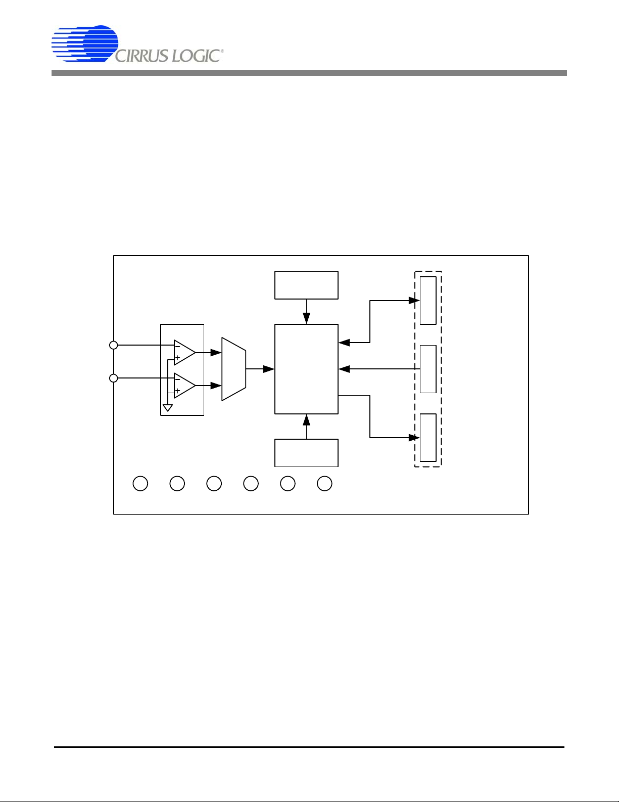
CS5581
M
U
X
VREF
4.096 V
XTAL
16 MHz
Communication/Control
Interface
Master/Slave
Serial Port
Digital Inputs
to ADC
Digital Outputs
from ADC
IN_A
IN_B
+2.5V GND -2.5V GND +3.3V GND
J8
J6
J7
CS3004
Single-ended
Analog Inputs
Figure 1. CDB5581 Block Diagram
1.1 Overview
The CDB5581 evaluation board has both analog and digital circuit sections. The analog section consists
of the CS5581 ADC, two analog input signal buffers, controlled through a multiplexer, that condition the
signal into the ADC, and a precision 4.096 V reference. The digital section consists of board operation
configuration control signals, reset circuitry, an SPI™ serial port, a jumper connection for initiating ADC
calibration, and an EEPROM for evaluation board identification.
The evaluation board operates from +2.5V, -2.5V, +3.3V and communicates through an SPI™ serial port.
Figure 1 illustrates the CDB5581 block diagram.
4 DS796DB3
Page 5
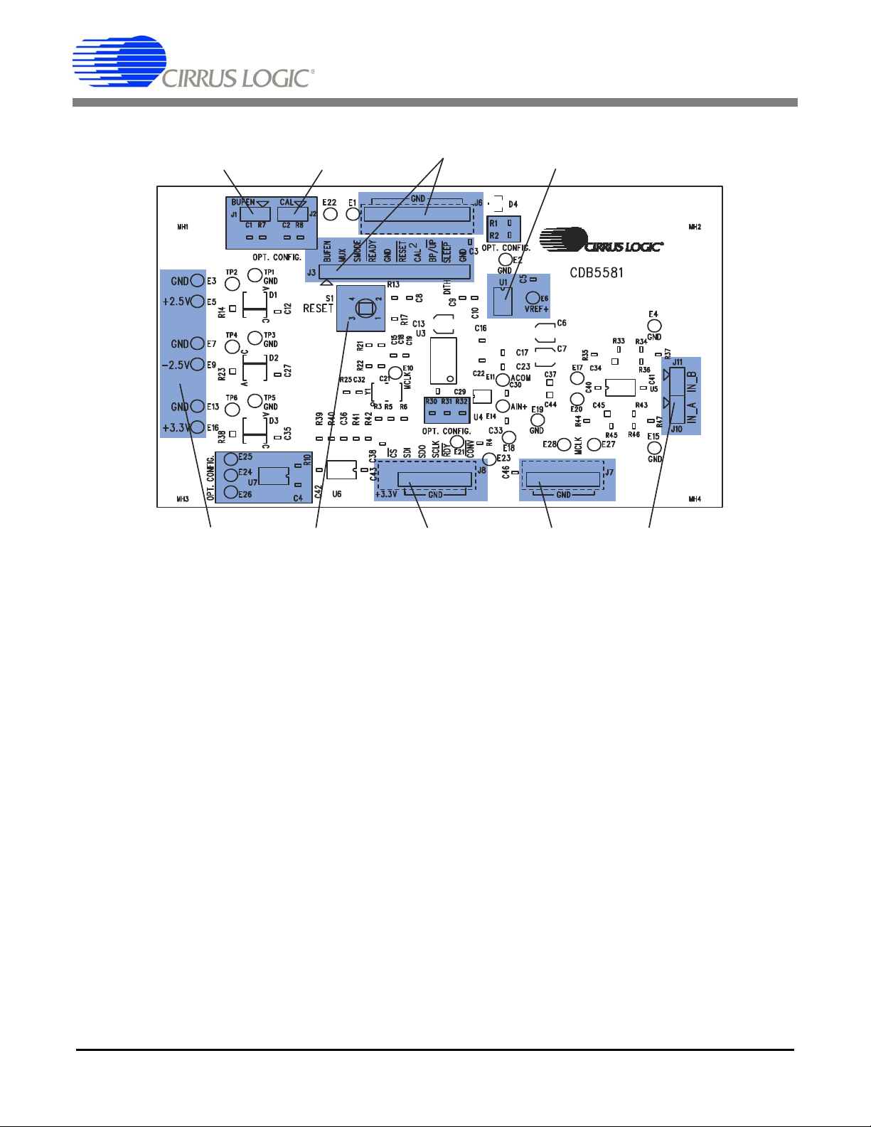
2. QUICK START
Master/Slave SPI ADC MCLK Out
Signals to ADC & Mux
Buffer Enable Calibrate 4.096 V Reference
ADC Reset Analog Inputs
DC Supply
NOTES:
1. Shaded boxes marked with "OPT. CONFIG." are not necessary for operation in an end user product.
2. Calibration function has been removed from the device but still appears on the PCB. J2 must be shorted (grounded)
for proper operation. See Appendix E for details.
2
Figure 2. CDB5581 Board Layout
CDB5581
The CDB5581 evaluation board is designed to interface with a data acquisition system. To connect and
configure the
CDB5581 perform the following initialization procedure:
1. Verify that the power supplies are off.
2. Connect the power supplies to the CDB5581 as shown in Table 1 on page 6.
3. Verify that the power is off to the analog input signal & control signal sources.
4. Connect the analog input signal source to the evaluation board per Table 2 on page 6. Verify from Table 4
on page 8 that the analog input channel selected is IN_A.
5. Configure the CDB5581 by connecting the control signal sources to the evaluation board as shown in
Table 3 on page 7. Apply logic-level inputs as required to override the resistor pull-ups/pull-downs.
6. Make connections to the SPI™ serial port connector as shown in Table 5 on page 8. The CS5581 ADC
serial port is configured by default to operate in the SSC (Synchronous Self Clocking) mode. Refer to the
CS5581 data sheet for more information on serial communication modes and signal timing.
7. Turn on the power supplies to the evaluation board.
8. Apply power to the signal source.
9. Press the Reset switch on the evaluation board.
10. The CS5581 ADC's SPI™ serial port should now be communicating data.
DS796DB3 5
Page 6
3. HARDWARE DESCRIPTION
3.1 Absolute Maximum Ratings
Observe the following limits to ensure the CDB5581 component ratings are not exceeded.
• CS5581
– The absolute maximum supply voltage that can be applied to the +3.3V power supply
connection is +3.6V.
– The absolute maximum power supply voltage that can be applied between pins VL and V1-
is 6.1 V.
• CS3004
– The absolute maximum power supply voltage that can be applied between the +2.5V and
-2.5V power supply connections is +5.5V.
3.2 Power Supply
Power supply connections and requirements are specified in Table 1. below.
Table 1. Power Supply Connections
CDB5581
Power Supply
Requirement
+2.5 V DC, ±5%, <50 mA E5 E3 TP2, TP1 (GND)
-2.5 V DC, ±5%, <50 mA E9 E7 TP4, TP3 (GND)
+3.3 V DC, ±5%, <50 mA E16 E13 TP6, TP5 (GND)
Power Supply
Connection
Associated
Ground Return
Associated
T est Points
Important: It is recommended that all power supplies be isolated from utility ground to prevent the introduction of a ground loop. One ground connection may already exist through the serial port connection to
utility ground. Using the Cirrus Logic CapturePlus II system simplifies making connections to the
CDB5581 by providing electrical isolation between the two.
Using twisted/shielded wire will reduce electrical noise induced onto the power supply cables.
Power supplies are to be adequately regulated and sufficiently low noise to meet the application requirements.
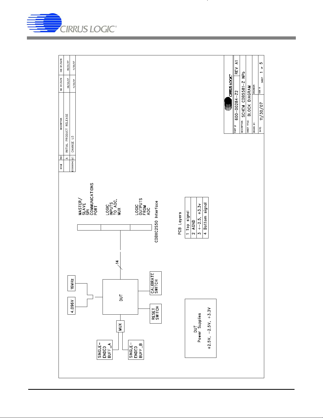
3.3 Analog Section
3.3.1 Analog Input Buffers
The analog input signal connections to the input buffers are made at the IN_A and IN_B connectors, as
specified in Table 2.
Table 2. Analog Input Connections
Analog Input
Channel
IN_A J10 -2.048 V to +2.048 V 50 Ohms
IN_B J11 -2.048 V to +2.048 V 50 Ohms
Connection
Input Signal
Voltage Range Impedance
There are two analog input channels on the evaluation board. Each analog input channel consists of a
low-noise amplifier configured as a unity gain non-inverting buffer. The buffers utilize a Cirrus Logic
CS3004 precision, low-noise, low-voltage, dual opamp.. These op-amps enable both the inputs and outputs of the analog input buffer to operate virtually rail to rail. The channel input impedance is 50 Ohms.
6 DS796DB3
Page 7
CDB5581
The analog inputs are designed for connections to single-ended input signals referenced to ground. The
usable input voltage range is -2.048 V to +2.048 V. The theoretical input frequency range of the CS5581
is from DC to the Nyquist frequency of 100 kHz. The analog input buffer amplifiers are configured for a
cutoff frequency of 16.8 kHz to band-limit noise into the ADC. Changing the cutoff frequency will change
the noise bandwidth accordingly.
3.3.2 Multiplexer
Analog input channel selection is controlled through the multiplexer. The multiplexer is configured with a
pull-down resistor on the MUX control line to enable input channel labeled "INPUT A" by default. To select
channel B, apply 3.3 V to the multiplexer input control line (MUX).
Signal levels for controlling the multiplexer that selects between analog input channels A and B is shown
in Table 3.
Table 3. Analog Input Channel Selection
Multiplexer
Control Input (MUX)
0V A
3.3 V B
Input Channel
Enabled
During multiplexing, the maximum sample rate for each channel is half that of the ADC’s maximum sample rate. Additionally, the Nyquist frequency for each channel is half of the ADC’s Nyquist frequency.
3.3.3 ADC Reset
The CS5581 ADC makes use of an externally generated power-on reset. Therefore, after power is applied to the ADC, the reset pin must be driven low then released. Pressing the Reset button generates a
reset cycle. A reset cycle can be generated at any time during ADC operation. The ADC RST
pin (active
low) is held inactive through a pull-up resistor.
3.3.4 Voltage Reference
The voltage reference IC provided generates a 4.096 V precision reference.
3.3.5 ADC Reference Frequency
The reference frequency for the CS5581 ADC is provided by a 16.000 MHz oscillator.
DS796DB3 7
Page 8
CDB5581
3.4 Digital Section
3.4.1 Hardware Configuration
The CDB5581 evaluation board hardware comes pre-configured so the only connection required between
it and a data acquisition system is the serial port connection.
The hardware setup is reconfigurable through the hardware control interface connectors. Configure the
evaluation board by setting the appropriate control line to the appropriate logic level.
Table 4. Hardware Configuration Signals
Function Default Level Label Connector Test Point
Input Channel Select = Selected (Low) MUX J6, Pin 16 J3, Pin 2
Analog Input Buffers Buffers = Enabled (High) BUFEN J1 J3, Pin1
Serial Port Mode Sync. Self Clock = Enabled (High) SMODE J6, Pin 12 J3, Pin 3
Data Ready Flag Data Ready When Set (Low) RDY
Reset Reset = Inactive (High) RST
Bipolar / Unipolar Mode Bipolar = Enabled (High) BP / UP J6, Pin 2 J3, Pin 8
Serial Port Communication Chip Select = Enabled (Low) CS J8, Pin 2 E23
Data Conversion Mode Continuous Conversion = Active (Low) CONV
J8, Pin 10 J3, Pin 4
J6, Pin 6; S1 J3, Pin 6
J8, Pin 12 E21
3.4.2 SPI™ Serial Port Communications
The CS5581 ADC communications port features an SPI™ serial port. It can be configured for SSC mode
(Master) or SEC mode (Slave) mode as shown in Table 4. Test points are provided to monitor serial communications.
Connections to the serial interface are made according to the following table.
Table 5. Serial Interface Connections
Function Label Connector Test Point
Chip Select CS
Serial Data Input SDI J8, Pin 4 E24
Serial Data Output SDO J8, Pin 6 E25
Serial Clock SCLK J8, Pin 8 E26
J8, Pin 2 E23
8 DS796DB3
Page 9

APPENDIX A. MAXIMIZING THE PERFORMANCE OF THE CS5581
A.1 PCB Layout Considerations
• Keep the signal path short between the CS5581 ADC input capacitors C37, C44 and the ADC
input pin to minimize trace inductance.
• The analog input buffer amplifiers and ADC input buffer capacitors are placed before the multi-
plexer. Placing the buffer amplifiers before the multiplexer allows the amplifiers driving the ADC
buffer capacitors to be fully settled when sampled by the ADC. Therefore, the multiplexer must
be of a low on-resistance type to prevent distortion or latency issues.
• Power supply noise is a major design consideration and the power supplies need adequate
bypassing and bulk capacitance.
• When operating the ADC from +2.5 V and -2.5 V split supplies, place the power supply & buffer
amplifier bypass capacitor ground connections close together.
• Keep all ground connections on each differential buffer amplifier as close to the device as pos-
sible to avoid introducing differential noise through high-impedance connections.
• Keep trace lengths short between the ADC and the voltage reference IC negative supply pins.
• Route the oscillator output away from analog circuitry.
CDB5581
• Use a solid ground plane in the PCB layout.
• Provide adequate separation between analog and digital signals.
• To minimize distortion within the analog signal path, consider using components with smaller
voltage dependencies.
• Minimize ADC digital output edge transition current loading.
A.2 Hardware Considerations
At a system level, use shielded cable for interconnects. Keep interconnect cable lengths as short as possible. Route analog and digital signals connecting to the PCB away from each other.
DS796DB3 9
Page 10

APPENDIX B. BILL OF MATERIALS
y
r
NYLON, 300-00002-Z1
CDB5581
MFG MFG P/N Notes
KEMET C0805C104K5RAC
BILL OF MATERIAL
Reference Designato
C21 C22 C23 C27 C29 C30 C32 C33 C35 C36
NO POP NP-PAD-040 NO POP
C38 C40 C41 C42 C43 C46
E16 E17 E18 E19 E20 E21 E22 E23 E24 E25
E26 E27 E28
Cirrus P/N Rev Description Qt
001-03713-Z1 A CAP 1000pF ±10% 50V X7R NPb 0805 2 C1 C2 KEMET C0805C102K5RAC
001-04345-Z1 A CAP 0.1uF ±10% 50V X7R NPb 0805 27 C3 C4 C5 C9 C10 C12 C15 C16 C17 C18 C19
012-00012-Z1 A CAP 10uF ±20% 16V ELEC NPb CASE A 3 C6 C7 C13 PANASONIC EEE1CS100SR
001-03987-Z1 A CAP 4700pF ±10% 50V X7R NPb 0805 1 C8 KEMET C0805C472K5RAC
001-05587-Z1 A CAP 120pF ±5% 100V C0G NPb 1206 2 C34 C45 KEMET C1206C121J1GAC
070-00111-Z1 A DIODE TR 6.8V 600W NPb DO-214AA 3 D1 D2 D3 LITTELFUSE P6SMBJ6.8A
070-00010-Z1 A DIODE SCHTKY BAR 30V 0.2A NPb SOT23 1 D4 PHILIPS BAT54
000-00025-Z1 A NO POP 040 PAD 064 NPb TH 0 E1 E2 E3 E4 E5 E6 E7 E9 E10 E11 E13 E14 E15
115-00052-Z1 A HDR 2x1 ML .1"CTR 093 GLD NPb 0 J1 J2 SAMTEC TSW-102-26-G-S NO POP
115-00217-Z1 A HDR 10X1 FML .1" 093 GLD NPb TH 0 J3 SAMTEC SSW-110-01-G-S NO POP
115-00239-Z1 A HDR 8X2 093BD FML .1" .331" NPb TH 1 J6 SAMTEC SSW-108-01-G-D
115-00238-Z1 A HDR 5X2 093BD FML .1" .331" NPb TH 1 J7 SAMTEC SSW-105-01-G-D
115-00241-Z1 A HDR 6X2 093BD FML .1" .331" NPb TH 1 J8 SAMTEC SSW-106-01-G-D
304-00012-Z1 A SPCR STANDOFF NYL HEX750/4-40TH NPb 4 MH1 MH2 MH3 MH4 KEYSTONE 1902D REQUIRES SCREW 4-40X1X4" PH
021-00435-Z1 A RES 10k OHM 1/8W ±5% NPb 0805 FILM 9 R1 R2 R7 R8 R31 R32 R39 R40 R42 DALE CRCW080510K0JNEA
021-00363-Z1 A RES 10 OHM 1/8W ±5% NPb 0805 FILM 4 R3 R21 R22 R25 DALE CRCW080510R0JNEA
020-02044-Z1 A RES 100k OHM 1/8W ±1% NPb 0805 FILM 5 R4 R5 R6 R10 R30 DALE CRCW0805100KFKEA
021-00387-Z1 A RES 100 OHM 1/8W ±5% NPb 0805 FILM 1 R13 DALE CRCW0805100RJNEA
020-02273-Z1 A RES 0 OHM 1/4W 1206 FILM 3 R14 R23 R38 DALE CRCW12060000Z0EA
021-00423-Z1 A RES 3.3k OHM 1/8W ±5% NPb 0805 FIL 1 R17 DALE CRCW08053K300JNEA
020-01848-Z1 A RES 2k OHM 1/8W ±1% NPb 0805 FILM 4 R33 R34 R45 R46 DALE CRCW08052K00FKEA
023-00002-Z1 A RES 49.9 OHM 1/10W ±5% NPb 0805 THN 2 R35 R44 SUSUMU RR1220Q-49R9-D-M
020-01816-Z1 A RES 1k OHM 1/8W ±1% NPb 0805 FILM 2 R36 R43 DALE CRCW08051K00FKEA
020-01667-Z1 A RES 49.9 OHM 1/8W ±1% NPb 0805 FILM 2 R37 R47 DALE CRCW080549R9FKEA
021-01430-Z1 A RES 33k OHM 1/8W ±5% NPb 0805 FILM 1 R41 DALE CRCW080533K0JNEA
120-00057-Z1 A SWT SPST 130G 0/1 7mm TACT ESD NPb 1 S1 ITT INDUSTRIES PTS645TL70 INSTALL AFTER WASH PROCESS
110-00045-Z1 A CON TEST PT .1"CTR TIN PLAT NPb BLK 3 TP1 TP3 TP5 KEYSTONE 5001
110-00024-Z1 A CON TEST PT .1" TIN PLT RED NPb TH 2 TP2 TP6 KEYSTONE 5000
110-00025-Z1 A CON TEST PT .1" TIN PLATE WHT NPb 1 TP4 KEYSTONE 5002
060-00351-Z1 A IC LNR PREC VREF 4.096Vout NPb SO8 1 U1 MAXIM MAX6126AASA41+
065-00261-Z2 B0 IC CRUS ADC 200kSps 14b NPb SSOP24 1 U3 CIRRUS LOGIC CS5581-ISZ/B0 ECO542
060-00352-Z1 A IC LNR ANA SW 4OHM SPDT NPb MSOP10 1 U4 MAXIM MAX4635EUB+
065-00219-Z1 A0 IC CRUS PREC DL LO-V AMP NPb SOIC8 1 U5 CIRRUS LOGIC CS3004-FSZ/A0
060-00386-Z1 A IC LNR DIFF COMP HS 5.25V NPb SOIC8 1 U6 TEXAS INSTRUMENTS TL712CD
062-00064-Z1 A IC PGM SPI EEPROM 8kX8 2MHz NPb SO8 1 U7 MICROCHIP 25LC640-I/SN
102-00097-Z1 A OSC 16MHz 50ppm 3.3V NPb SMD 3x5 1 Y1 ABRACON ASFL1-16.000MHZ-EC-T
603-00284-Z1 A ASSY DWG CDB5571-1-Z NPb REF CIRRUS LOGIC 603-00284-Z1
240-00284-Z1 A PCB CDB5571-1-Z NPb 1 CIRRUS LOGIC 240-00284-Z1
600-00284-Z2 A1 SCHEM CDB5581-Z NPb REF CIRRUS LOGIC 600-00284-Z2 ECO542
300-00002-Z1 A SCREW 4-40X1/4" PH NYLON NPb 4 XMH1 XMH2 XMH3 XMH4 BUILDING FASTENERS NY PMS 440 0025 PH
CIRRUS LOGIC
CDB5581_REV_A1.PL
001-06472-Z1 A CAP 4700pF ±5% 50V C0G NPb 1206 2 C37 C44 KEMET C1206C472J5GAC
10 DS796DB3
Page 11
APPENDIX C. SCHEMATICS
Figure 3. Schematic - Block Diagram
CDB5581
DS796DB3 11
Page 12

Figure 4. Schematic - Power Supplies
CDB5581
12 DS796DB3
Page 13
Figure 5. Schematic - Input Buffers and Multiplexer
CDB5581
DS796DB3 13
Page 14

Figure 6. Schematic - CS5581
CDB5581
14 DS796DB3
Page 15
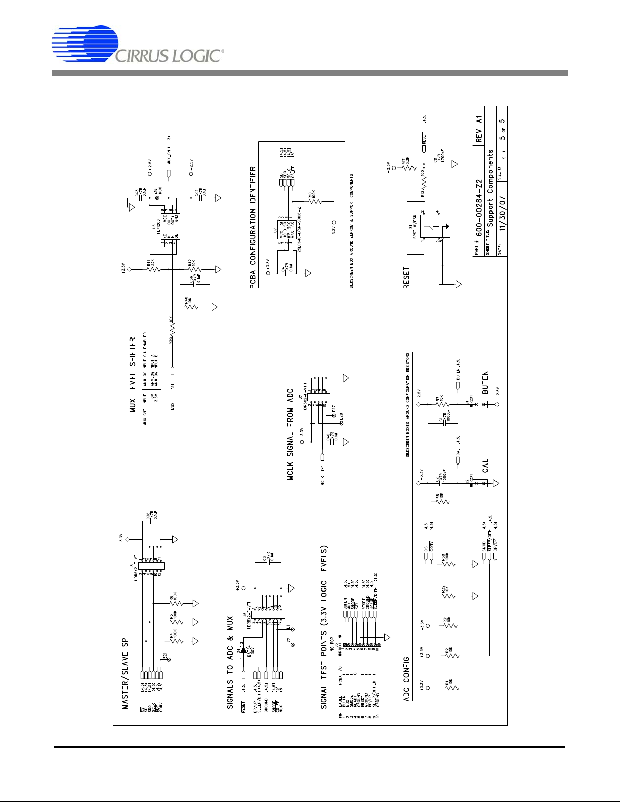
Figure 7. Schematic - Configuration & Misc.
CDB5581
DS796DB3 15
Page 16

APPENDIX D. LAYER PLOTS
Figure 8. Top Silkscreen
Calibration function has been removed from the device but still appears on the PCB. J2 must be shorted (grounded)
for proper operation. See Appendix E for details.
CDB5581
16 DS796DB3
Page 17

Figure 9. Top Solder Mask
CDB5581
DS796DB3 17
Page 18

Figure 10. Top Routing
CDB5581
18 DS796DB3
Page 19

Figure 11. Ground Plane
CDB5581
DS796DB3 19
Page 20

Figure 12. Power Plane
CDB5581
20 DS796DB3
Page 21

Figure 13. Bottom Solder Mask
CDB5581
DS796DB3 21
Page 22

Figure 14. Bottom Silkscreen
CDB5581
22 DS796DB3
Page 23

Figure 15. Top Solder Paste Mask
CDB5581
DS796DB3 23
Page 24

Figure 16. Bottom Routing
CDB5581
24 DS796DB3
Page 25

CDB5581
APPENDIX E. CALIBRATION FUNCTION
The calibration function has been removed from the CS5581. All references to calibration have been removed from this document. However, calibration still appears on the PCB. A jumper must be added to J2
for proper operation.
DS796DB3 25
Page 26

REVISION HISTORY
Contacting Cirrus Logic Support
For all product questions and inquiries contact a Cirrus Logic Sales Representative. To find the one nearest to you
go to www.cirrus.com
IMPORTANT NOTICE
Cirrus Logic, Inc. and its subsidiaries ("Cirrus") believe that the information contained in this document is accurate and reliable. However, the information is subject
to change without notice and is provided "AS IS" without warranty of any kind (express or implied). Customers are advised to obtain the latest version of relevant
information to verify, before placing orders, that information being relied on is current and complete. All products are sold subject to the terms and conditions of sale
supplied at the time of order acknowledgment, including those pertaining to warranty, indemnification, and limitation of liability. No responsibility is assumed by Cirrus
for the use of this information, including use of this information as the basis for manufacture or sale of any items, or for infringement of patents or other rights of third
parties. This document is the property of Cirrus and by furnishing this information, Cirrus grants no license, express or implied under any patents, mask work rights,
copyrights, trademarks, trade secrets or other intellectual property rights. Cirrus owns the copyrights associated with the information contained herein and gives
consent for copies to be made of the information only for use within your organization with respect to Cirrus integrated circuits or other products of Cirrus. This consent does not extend to other copying such as copying for general distribution, advertising or promotional purposes, or for creating any work for resale.
CERTAIN APPLICATIONS USING SEMICONDUCTOR PRODUCTS MAY INVOLVE POTENTIAL RISKS OF DEATH, PERSONAL INJURY, OR SEVERE PROPERTY OR ENVIRONMENTAL DAMAGE ("CRITICAL APPLICATIONS"). CIRRUS PRODUCTS ARE NOT DESIGNED, AUTHORIZED OR WARRANTED FOR
USE IN PRODUCTS SURGICALLY IMPLANTED INTO THE BODY, AUTOMOTIVE SAFETY OR SECURITY DEVICES, LIFE SUPPORT PRODUCTS OR OTHER
CRITICAL APPLICATIONS. INCLUSION OF CIRRUS PRODUCTS IN SUCH APPLICATIONS IS UNDERSTOOD TO BE FULLY AT THE CUSTOMER'S RISK
AND CIRRUS DISCLAIMS AND MAKES NO WARRANTY, EXPRESS, STATUTORY OR IMPLIED, INCLUDING THE IMPLIED WARRANTIES OF MERCHANTABILITY AND FITNESS FOR PARTICULAR PURPOSE, WITH REGARD TO ANY CIRRUS PRODUCT THAT IS USED IN SUCH A MANNER. IF THE CUSTOMER
OR CUSTOMER'S CUSTOMER USES OR PERMITS THE USE OF CIRRUS PRODUCTS IN CRITICAL APPLICATIONS, CUSTOMER AGREES, BY SUCH USE,
TO FULLY INDEMNIFY CIRRUS, ITS OFFICERS, DIRECTORS, EMPLOYEES, DISTRIBUTORS AND OTHER AGENTS FROM ANY AND ALL LIABILITY, INCLUDING ATTORNEYS' FEES AND COSTS, THAT MAY RESULT FROM OR ARISE IN CONNECTION WITH THESE USES.
Cirrus Logic, Cirrus, and the Cirrus Logic logo designs are trademarks of Cirrus Logic, Inc. All other brand and product names in this document may be trademarks
or service marks of their respective owners.
SPI is a trademark of Motorola, Inc.
PADS and PowerLogic are trademarks of Mentor Graphics.
National Semiconductor is a registered trademark of National Semiconductor Corporation.
Revision Date Changes
DB1 AUG 2007 Initial Release.
DB2 DEC 2007 Updated schematic to reflect new silicon revision.
DB3 OCT 2009 Removed calibration function / added Appendix E.
CDB5581
26 DS796DB3
 Loading...