

Page 1
CDB5530U
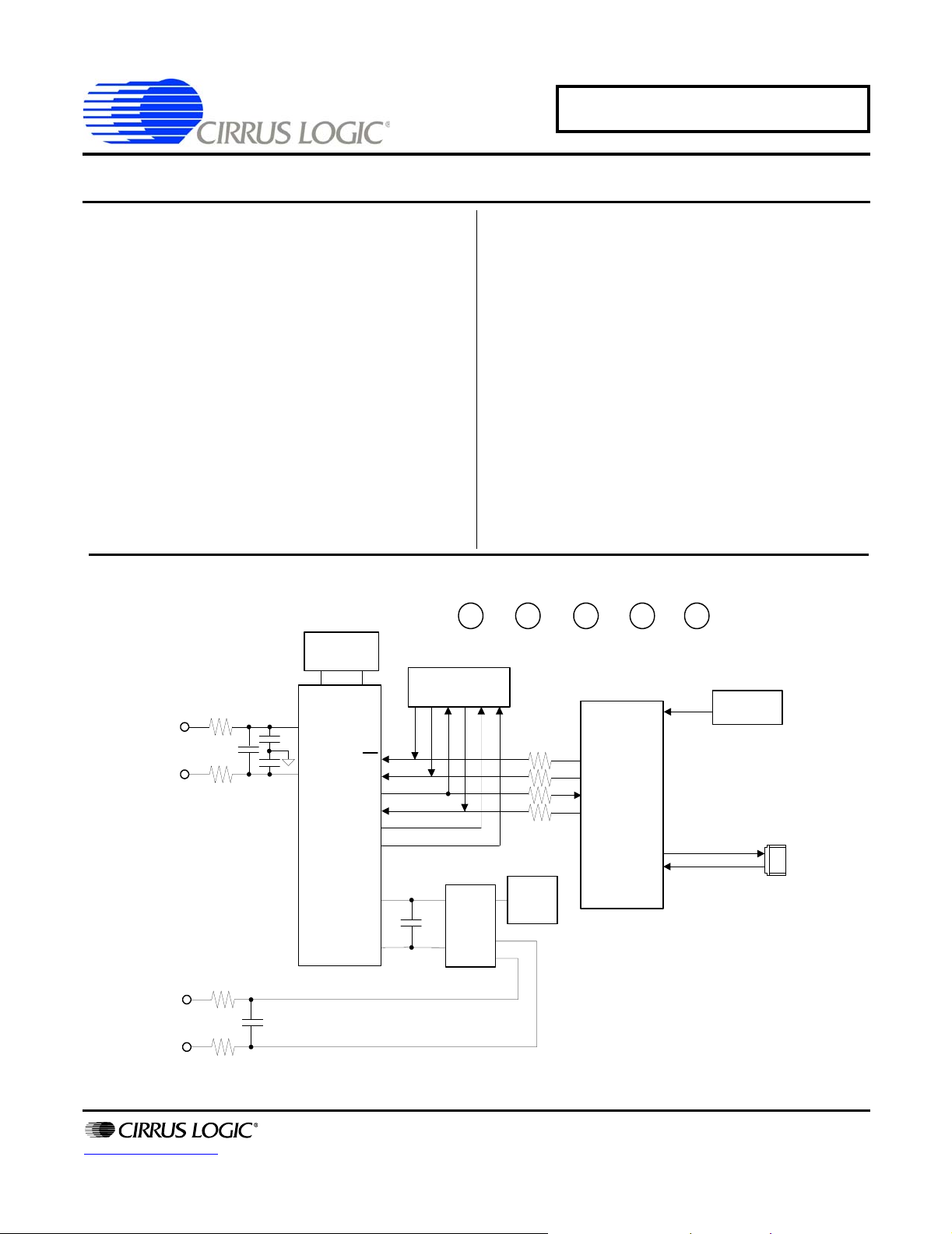
CDB5530U Evaluation Board and Software
Features
USB Communication with PC
On-board Microcontroller
On-board Voltage Reference
Evaluation Software
– Register Setup & Chip Control
– FFT Analysis
– Time Domain Analysis
– Noise Histogram Analysis
Interface Header for External Microcontroller
CRYSTAL
4.9152 MHz
General Description
The CDB5530U is an inexpensive tool designed to evaluate the functionality and performance of the CS5530.
The CS5530 data sheet should be read and consulted
when using the CDB5530U evaluation board.
The evaluation board includes a C8051F320 microcontroller with a USB interface. The microcontroller controls
the serial communication between the evaluation board
and the PC via the firmware, enabling quick and easy access to all of the CS5530’s registers and functions.
The CDB5530U includes software for Data Capture,
Time Domain Analysis, Histogram Analysis, and Frequency Domain Analysis.
ORDERING INFORMATION
CDB5530U Evaluation Board
VA- VA+
GND
VD+
+5 V
AIN1+
AIN1-
VREF+
VREF-
CS5530
AIN1+
AIN1-
CS
SDI
SDO
SCLK
A0
A1
VREF+
VREF-
Interface Header
VREF
Source
Select
LT1019
C8051F320
Microcontroller
RESET
CIRCUITRY
CONNECTOR
USB
http://www.cirrus.com
Copyright © Cirrus Logic, Inc. 2006
(All Rights Reserved)
NOV ‘06
DS742DB1
Page 2

TABLE OF CONTENTS
1. HARDWARE .............................................................................................................................3
1.1 Introduction ............................ .... ... ... ... ... .... ... .....................................................................3
1.2 Evaluation Board Overview ..................................................................... ... ........................3
1.2.1 Analog Section ....................................... .... ... ... ... .... ... ... ... ..................................... 3
1.2.2 Digital Section ........ ... .... ... ... ....................................... ... ... ... .... ... ... ........................ 4
1.2.3 Power Supply Section ............................................. ... ... ........................................ 4
2. SOFTWARE .............................................................................................................................. 8
2.1 Installation Procedure ...................................................................... .... ... ... ... .... .................8
2.2 Using the Software ................................. .... ... ..................................................................... 8
2.2.1 Start-Up Window ................................................. .... ... ... ........................................ 8
2.2.2 Setup Window .......................................................................................................9
2.2.3 Data Collection Window ......................................................................................12
2.2.4 Configuration Window ................................................ ... ... ................................... 13
2.3 Collecting Data Sets ........................................................................................................14
2.4 Saving and Printing Data .................................................................................................14
2.5 Retrieving Saved Data From a File ..................................................................................14
2.6 Analyzing Data ....... .......................................... ... .... .......................................... ... ............14
2.7 Histogram Information ......................................................................................................15
2.8 Frequency Domain Information ..................... ... ... .... ...................................... .... ... ... ... ......15
2.9 Time Domain Information ................................................................................................. 15
3. BOARD LAYOUT ................................................................................................................... 16
CDB5530U
LIST OF FIGURES
Figure 1. Analog Section................................................................................................................. 5
Figure 2. Digital Section .................................................................................................................. 6
Figure 3. Power Supply................................................................................................................... 7
Figure 4. Evaluation Software Start-Up Screen .............................................................................. 8
Figure 5. CDB5530U Setup Window............................................................................................... 9
Figure 6. CDB5530U Calibration Window.....................................................................................10
Figure 7. CDB5530U Data Collection Window..............................................................................12
Figure 8. CDB5530U Configuration Window.................................................................................13
Figure 10. Top Silkscreen .............................................................................................................16
Figure 11. Top Side Layout...........................................................................................................17
Figure 12. Bottom Silkscreen........................................................................................................18
Figure 13. Bottom Side Layout...................................................................................................... 19
LIST OF TABLES
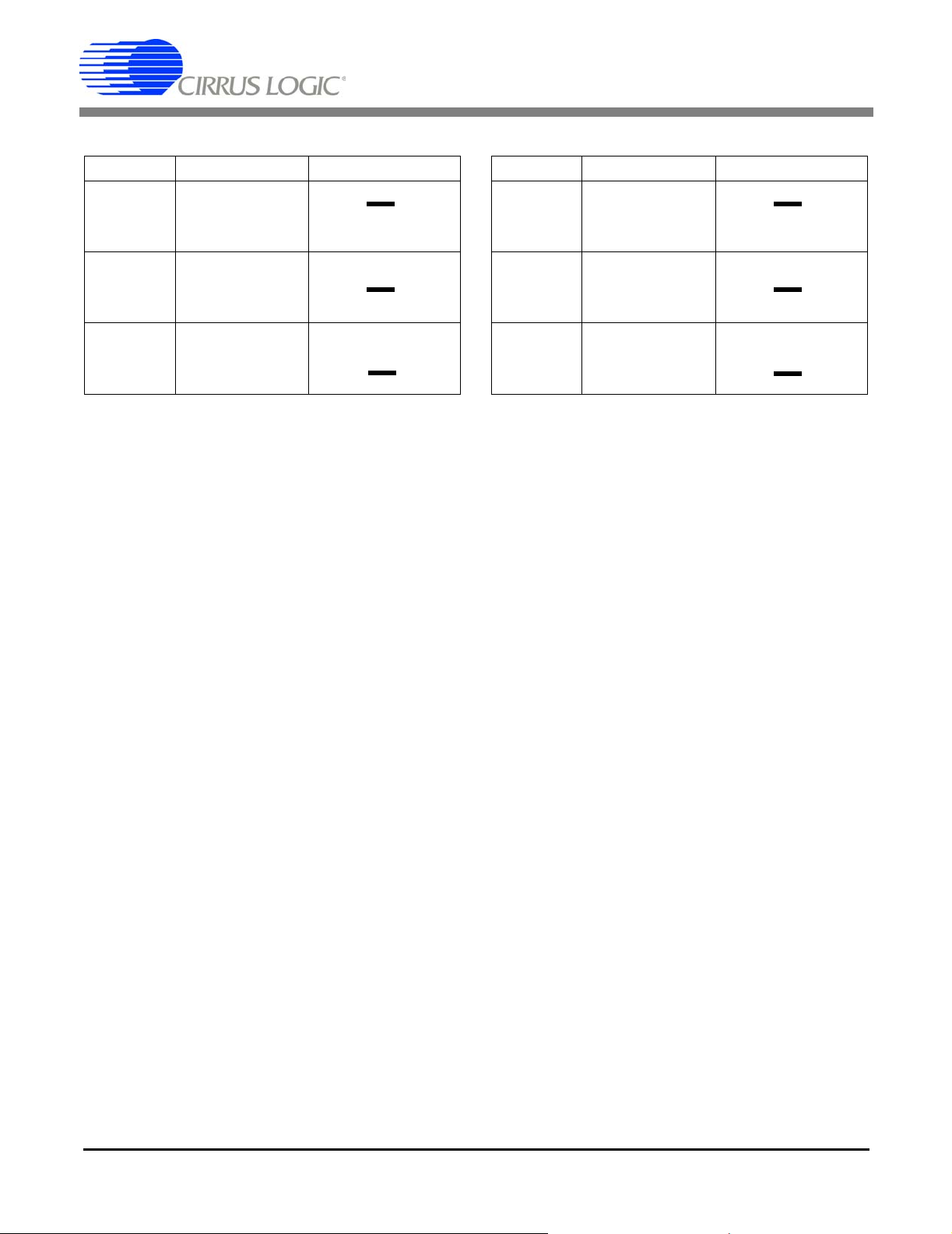
Table 1. Voltage Reference Selection for VREF+ ..........................................................................4
Table 2. Voltage Reference Selection for VREF- ...........................................................................4
2 DS742DB1
Page 3

CDB5530U
1. HARDWARE
1.1 Introduction
The CDB5530U evaluation board provides a quick means of evaluating the CS5530 Analog-to-Digital
Converter (ADC). The CS5530 is a highly integrated ∆Σ ADC which uses charge-balance techniques to
achieve 24-bit performance. The CS5530 includes a very low noise chopper-stabilized instrumentation
amplifier (12 nV/sqrt(Hz) @ 0.1 Hz) with a fixed gain of 64×. This ADC also includes a fourth-order ∆Σ
modulator followed by a digital filter which provides twenty selectable output word rates of 6.25 Hz,
7.5 Hz, 12.5 Hz, 15 Hz, 25 Hz, 30 Hz, 50 Hz, 60 Hz, 100 Hz, 120 Hz, 200 Hz, 240 Hz, 400 Hz, 480 Hz,
800 Hz, 960 Hz, 1.6 kHz, 1.92 kHz, 3.2 k Hz and 3.84 kHz (XIN = 4.9152 MHz).
1.2 Evaluation Board Overview
The CDB5530U evaluation board is partitioned into two main sections — analog and digital. The analog
section consists of the CS5530 and a precision voltage reference. The digital section consists of the microcontroller, the reset circuitry, and the USB interface. The board also has power supply connections
which accommodate all of the various supply options of the CS5530.
The evaluation board’s analog section operates from either a single +5 V, dual ±2.5 V, or dual ±3 V power
supply. The evaluation board interfaces the CS5530 to an IBM
accomplish this, the board comes equipped with a microcontroller and a USB cable which physically interfaces the evaluation board to the PC. The software provides easy access to the internal registers of the
CS5530, and provides a means to display and evaluate the performance of the ADC in the time domain
or the frequency domain.
®
compatible PC with a USB interface. To
1.2.1 Analog Section
The CS5530 is a high-precision ∆Σ converter designed to accurately measure one fully differential analog
voltage input while operating from a 4.9152 MHz crystal.
The evaluation board provides screw terminals labeled AIN1+ & AIN1- to connect input signals to the single input channel. The sensor’s output is filtered by a simple RC network at the channel input to reduce
any interference picked up by the input leads. The 3 dB corner of the filter is approximately 52 kHz, differential and 56 kHz, common mode. Figure 1 illustrates the schematic of the analog section.
The evaluation board provides three voltage reference options for VREF+ and VREF-. The three reference options for VREF+ include: VA+, the on-board LT1019 voltage reference, and external input (J12).
Table 1 illustrates the options available. With the J17 jumper in the VA+ position, the reference is supplied
by the VA+ analog supply. With the J17 jumper in the LT1019 position, the LT1019 provides a +2.5 V reference (the LT1019 was chosen for its low drift, typically 5ppm/°C). By setting the J17 jumper to the
VREF+ position, the user can supply an external voltage reference to J12’s VREF+ input.
The three reference options for VREF- include: VA-, GND, and external input (J12). Table 2 illustrates the
options available. With the J18 jumper in the VA- position, the reference is supplied by the VA- analog
supply. With the J18 jumper in the GND position, the VREF- pin is connected to the board ground. By
setting the J18 jumper to the VREF- position, the user can supply an external voltage reference to J12’s
VREF- input.
DS742DB1 3
Page 4
CDB5530U
Table 1. Voltage Reference Selection for VREF+ Table 2. Voltage Reference Selection for VREF-
Reference Description J17
VA+
LT1019
VREF+
Selects Positive
Analog Power
Supply
Selects on-Board
LT1019 Reference
(5ppm/
°C)
Selects External
Reference Source
(J12)
VA+
LT1019
REF+
VA+
LT1019
REF+
VA+
LT1019
REF+
O O VREF+
O O VREF+
O O VREF+
O O VREF+
O O VREF+
O O VREF+
O O VREF+
O O VREF+
O O VREF+
Reference Description J18
VA-
GND
VREF-
Selects Negative
Analog Power
Supply
Selects Board
Gnd
Selects External
Reference Source
(J12)
VA GND
REF-
VA GND
REF-
VA GND
REF-
O O VREFO O VREFO O VREF-
O O VREFO O VREFO O VREF-
O O VREFO O VREFO O VREF-
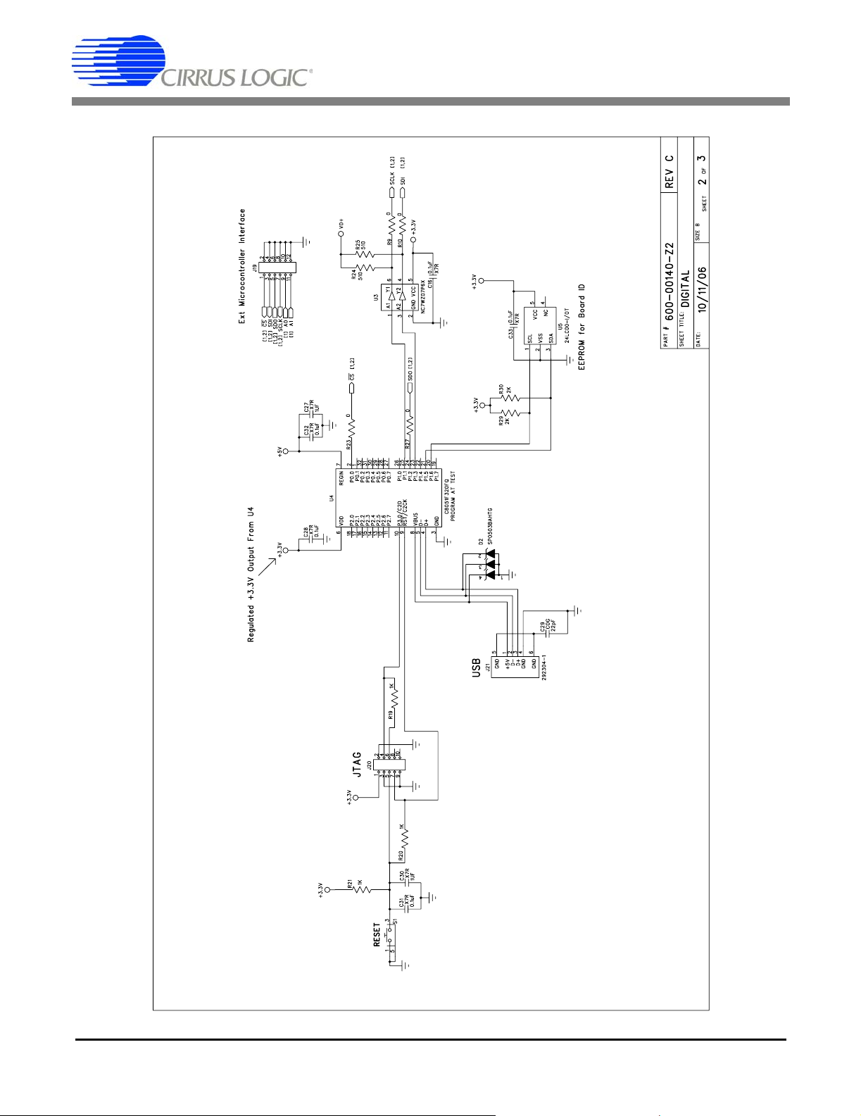
1.2.2 Digital Section
Figure 2 illustrates the schematic of the digital section. It contains the microcontroller, USB interface, EEPROM, JTAG header, reset circuitry, and an external interface header. The microcontroller interfaces the
™
SPI
and MICROWIRE™ compatible serial port of the CS5530 with the USB connection to the PC. Note
that the SCLK and SDI signals are level shifted to support both +3.3 V and +5 V digital operation.
The microcontroller EEPROM is used to store firmware. An external interface header, J19, is provided to
allow the CDB5530U to be interfaced with an external microcontroller. To use this serial interface, the
0 ohm resistors R9, R10, R23, and R27 should be removed to disconnect the on-board microcontroller
from the serial interface.
1.2.3 Power Supply Section
Figure 3 illustrates the power supply connections to the evaluation board. VA+ supplies the positive analog supply for the CS5530 and the LT1019 reference. Header J14 allows the VA+ supply to be sourced
from either the VA+ binding post (J2), or from the +5 V binding post (J3). VA- supplies the negative analog
supply for the analog section. Header J13 allows the VA- supply to be sourced from either the VA- binding
post (J1), or connected to the board ground. Note that the VA- supply should be connected to ground
when powering the CDB5530U from a single +5 V analog supply. VD+ supplies the digital section of the
ADC and level shifters. Header J15 allows the VD+ supply to be sourced from the VD+ binding post (J5),
the +5 V binding post (J3), or the regulated +3.3 V supply derived from the microcontroller. The +5 V binding post supplies the microcontroller’s internal regulator.
4 DS742DB1
Page 5
CDB5530U
Figure 1. Analog Section
DS742DB1 5
Page 6
CDB5530U
Figure 2. Digital Section
6 DS742DB1
Page 7

CDB5530U
Figure 3. Power Supply
DS742DB1 7
Page 8

CDB5530U
2. SOFTWARE
The evaluation board comes with software and a USB cable to link the evaluation board to the PC. The
software is designed to run under Windows
Important: DO NOT connect the evaluation board to the PC until you have completed the installa tion procedure and
have installed the USB drivers as described below.
2.1 Installation Procedure
2.1.1 CDB5530U GUI Software Installation Instructions
1. Ensure the CDB5530U USB cable is disconnected from the PC.
®
2000 or later.
2. Open GUI software installation folder CDB553x_cvidistkit.Eval5534U
3. Run SETUP.EXE by double clicking on the filename.
4. Select Next, I Accept License Agreement, Next, Next, Finish.
2.1.2 Installing the USB Drivers
1. Apply power to the CDB5530U. Press and release the Reset switch, S1.
2. Use the included USB cable to connect the CDB5530U to the PC. The PC operating system should
automatically launch the Found New Hardware wizard.
3. From the installation wizard, select Install from a list or specific location (Advanced). Select Search
for the best driver in these locations.
4. Select Include this location in the search.
5. Click the Browse... button.
6. Go to folder C:/Program Files/Eval5534U/Driver and click OK.
7. Press the Next button.
8. A Hardware Installation dialog will appear. Press Continue Anyway.
9. Select Browse... and go to folder C:/Program Files/Eval5534U/Driver. Press Open.
10. A Files Needed dialog will appear. Press OK.
11. The Found New Hardware wizard will appear. Press the Finish button.
Ö
Volume1.
2.1.3 Running the GUI
Run the program by selecting StartÖAll ProgramsÖEval5534UÖEval5534_U.
2.2 Using the Software
Before launching the evaluation program, the user should select the proper jumper settings as described
in Section 1.
8 DS742DB1
Page 9

CDB5530U
2.2.1 Start-Up Window
When the evaluation program is launched, the Start-Up window will appear. This window contains information concerning the software’s title, revision number, copyright date, etc.
Figure 4. Evaluation Software Start-Up Screen
At the top of the screen is a menu bar which displays user optio ns. The menu bar item Window is initially
disabled to prevent conflicts with other serial communications devices. After selecting the data source in
the Options menu, the Window menu item will become available.
2.2.1.1 Options
The Options menu item allows the user to select the source of the data and to configure the appearance
of the graphs. The user has two options for the data source: USB and File. If the USB setup is selected,
the evaluation software will be ready to communicate with the CDB5530U via the USB connection. At this
point, the Part menu item is active and the appropriate CS5530U device can be selected. If the File source
is selected, the evaluation software will prompt the user to select the appropriate data file. This option a llows the user to view previously captured data without having a CDB5530U connected to the PC. See
Section 2.5, "Retrieving Saved Data From a File" on page 14 for more details.
The Plot Options window can be accessed by pulling down the Options menu an d clicking on Plot Options.
In this window, the user can change the background color, the p lot line color, and the peak indicator color.
The harmonic and peak indicators can also be turned on or off in this window.
DS742DB1 9
Page 10

CDB5530U
2.2.1.2 Window
After the user selects the appropriate setup, the Window option becomes available in the Start-Up window. The Window pull-down has three options: Start-Up Window, Setup Window, and Data Collection
Window.
2.2.2 Setup Window
The Setup window allows the user to access the internal registers of the CS5530. See Figure 5.
Figure 5. CDB5530U Setup Window
In the Setup window, all of the ADC’s registers are displayed as hexadecimal values. The Configuration
register’s settings are also defined in this window.
Update Registers: The Update Registers button will read all the register values from the CS5530 and
update the hexadecimal values displayed on the screen. It is a good idea to press the Update Registers
button when entering the Setup window, or after modifying any registers to reflect the current status of the
part.
Reset Serial Port: When this button is pressed, the software will send the synch ronization sequence (dis-
cussed in the CS5530 data sheet) to the ADC. This sequence brings the CS5530’s serial port back to the
command mode, but does not reset any of the registers in the part.
Reset Part: When this button is selected, a ‘1’ is written to the RS bit in the Configuration register to reset
the part. After a reset, the registers will all return to their default values as discussed in the CS5530 data
sheet.
Read Data: This button will instruct the ADC to begin performing repeated single (fully-settled) conversions on the setup channel specified by the Setup Register box. The results of the most recent conversion
10 DS742DB1
Page 11
CDB5530U
are displayed in the Conversion Data box, as well as the Channel (always “1” for CS5530) and Overflow
indicator bits for each conversion. The software will halt the data collection process when the user presses
the Stop button.
Configuration Register: In the Configuration Register box, the contents of the Co nfiguration register are
displayed, and can be modified by typing a hexadecimal value in the Hexadecimal: box, or by changing
any of the values below the Hexadecimal: box to the desired settings.
Note: When changing the value of the reset system bit to “1” (RS, bit 29 in the Configuration register), the part will
be reset, and all registers will return to their default values. It is a good idea to select the Update Registers button
after performing a reset to update the screen with the new register values.
Offset / Gain Registers: In the Offset Registers / Gain Registers box, the contents of the offset and gain
registers are displayed in hexadecimal. These registers can all be modified in the Calibration window,
which is accessed when the user selects the Calibration Window button.
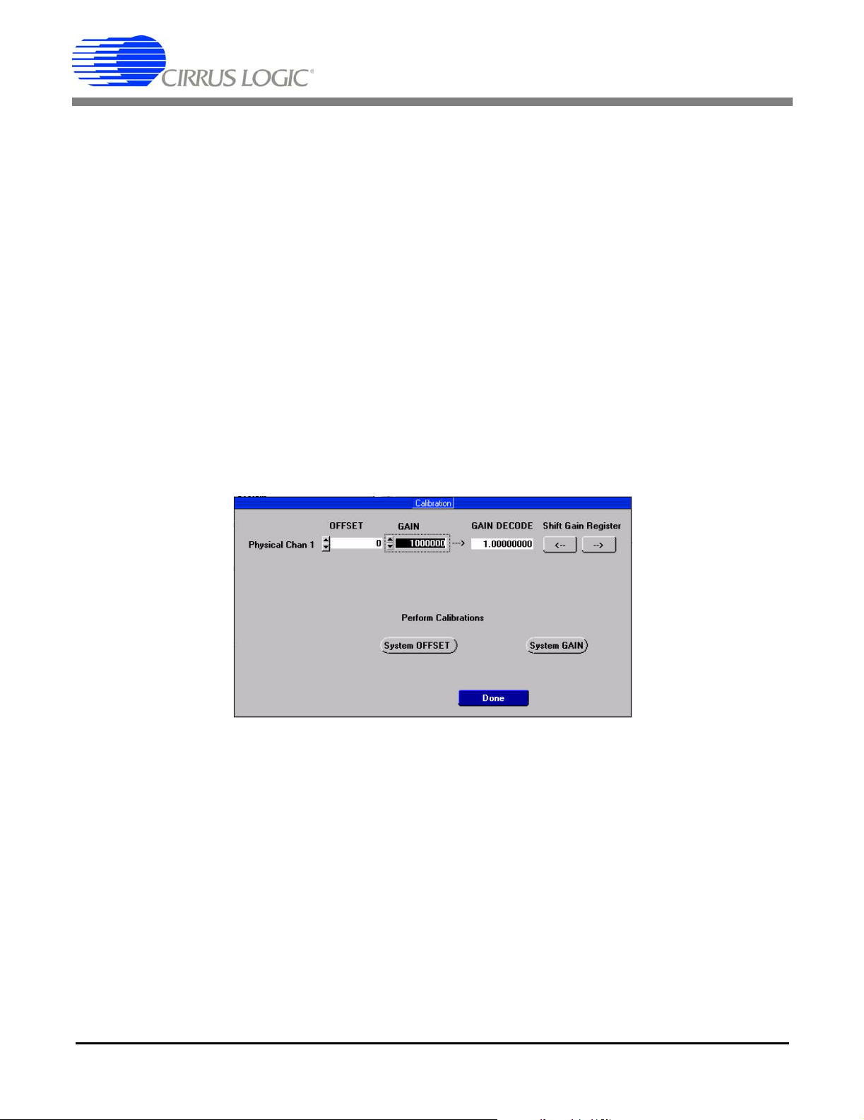
Calibration Window: The Calibration window (Figure 6) permits the user to access the ca libration registers of the CS5530 and also perform system offset or gain calibrations. Prior to performing calibrations
however, the Configuration register should be modified to configure the part for the desired operating
mode (see Section 2.2.4, "Configuration Window" on page 13 for more details). Note that offset calibration
should be performed before gain calibration to ensure accurate results. Refer to the CS5530 data sheet
for more details.
Figure 6. CDB5530U Calibration Window
System Offset Calibrations:
1) Attach an input signal to the AIN± inputs that you want to calibrate as zero. Note that the grounded
input must be within the common mode range of the amplifier for proper operation.
2) Activate the system offset calibration by pressing the System OFFSET button.
3) When the calibration is complete, the screen will automatically update the offset register with the
new value.
System Gain Calibrations:
1) Attach a full-scale input to the AIN± inputs of the CDB5530U.
2) Activate the system gain calibration by pressing the System GAIN button.
3) When the calibration is complete, the screen will automatically update the gain register with the
new values.
DS742DB1 11
Page 12

CDB5530U
2.2.3 Data Collection Window
The Data Collection window (Figure 7) allows the user to collect sample sets of data from the CS5530 and
analyze them using time domain, FFT, and histogram plots. The Data Collection window is accessible
through the Window option, or by pressing <F3>.
Figure 7. CDB5530U Data Collection Window
Time Domain / FFT / Histogram Selector: This menu selects the type of data processing to perform on
the collected data and display in the plot area. Refer to Section 2.6, "Analyzing Data" on page 14 for more
information.
Collect Button: This button will collect data from the part, to be analyzed in the plot area. See Section
2.3, "Collecting Data Sets" on page 14 for more information.
Config Button: This button will bring up the Configuration window, in which the u ser can modify th e data
collection specifications. See Section 2.2.4, "Configuration Window" on page 13.
Output Button: This button will bring up a window in which the user can output the data to a data file for
later use, print out a plot, or print out the entire screen.
Zoom Button: This button allows the user to zoom in on the plot by sele cting two poin ts in th e plot are a.
Press the Restore button to return to the normal data plot, or press the Zoom button again to zoom in even
further.
Setup Select Box: This box does not apply to the CS5530 as this device doe not contain a Setup register.
12 DS742DB1
Page 13

CDB5530U
2.2.4 Configuration Window
The Configuration window allows the user to set up the data collection a nd analysis parameters. See Figure 8.
Figure 8. CDB5530U Configuration Window
Number of Samples: This box allows the user to select the number of samples to collect, between 16
and 32,768.
Average: When doing FFT processing, this box will determine the number of FFTs to average. FFTs will
be collected and averaged when the Collect button is pressed.
FFT Window: This box allows the user to select the type of windowing algorithm for FFT processing. Windowing algorithms include the Blackman, Blackman-Harris, Hanning, 5-term Hodie, and 7-term Hodie.
The 5-term Hodie and 7-term Hodie are windowing algorithms developed by Cirrus Logic. This selection
has no effect on Time Domain or Histogram analysis.
Histogram Bin Width: This box allows for a variable "bin width" when plotting histograms of the collected
data. Each vertical bar in the histogram plot will contain the number of output codes contained in this box.
Increasing this number may allow the user to view histograms with larger input ranges.
Crystal Frequency: The CDB5530U evaluation board comes equipped with a 4.9152 MHz crystal. If the
user chooses to replace this with a crystal of a different frequency, the number in this box can be modified
to provide more accurate timing and FFT information.
Grounded FFT Test: When turned on, this function will generate an ideal full-scale sine wave for calculation purposes. This will enable the software to calculate the signal-to-distortion and signal-to-noise of
the converter with a simulated ideal full-scale sine wave source, although the converter is grounded.
Accept: When this button is selected, the current settings will be saved, and the user will return to the
Data Collection window.
DS742DB1 13
Page 14

CDB5530U
2.3 Collecting Data Sets
To collect a sample data set:
1) In the Data Collection window, select the Config button to bring up the Configuration window and
view the current settings.
2) Select the appropriate settings from the available options (see Section 2.2.4, "Configuration Win-
dow" on page 13) and press the Accept button.
3) The Data Collection window should still be visible. In the Setup box, select the Setup number you
want to use to perform conversions.
4) Select the Collect button to begin collecting data.
5) Data is sent directly to the PC through the USB cable. Depending on the value of the WR bits in
the selected Setup and the number of samples being collected, this process may take several minutes. The process can be terminated by pressing the Stop button, but if this is done, the user
should also press Reset on the CDB5530U board to bring the microcontroller out of the collection
routines.
6) Once the data has been collected, it can be analyzed, printed, or saved to disk.
2.4 Saving and Printing Data
Once collected, data can be printed or saved to a file for later use. To save or print data, click on the Output
button in the Data Collection window. A small panel will pop up with three options:
1) Output Data File: Brings up the File Save dialog box, which allows the data to be saved to a file.
2) Print Screen: Prints the entire display, including the calculated statistics.
3) Print Graph: Prints the information in the plot area. The statistical information is not printed.
2.5 Retrieving Saved Data From a File
To load a previously saved file:
1) Pull down the Setup option and select Disk. A file menu will appear.
2) Find the data file in the list and select it. Press the Select button to return.
3) Go to the Data Collection window, and press the Collect button.
4) The data from the file should appear on the screen. To select a different file, repeat the procedure.
2.6 Analyzing Data
The evaluation software provides three types of analysis - Time Domain, Frequency Domain, and Histo-
gram. The Time Domain analysis processes acquired conversions to produce a plot of conversion sample
number versus magnitude. The Frequency Domain analysis processes acquired conversions to produce
a magnitude-versus-frequency plot using the Fast-Fourier transform (results up to Fs/2 are calculated and
plotted). Also, performance parameters are also calculated and displayed. The Histogram analysis processes acquired conversions to produce a histogram plot. Statistical noise calculations are also calculated and displayed. For more information on Histograms, refer to Application Note AN37,
Analysis”.
“Noise Histogram
14 DS742DB1
Page 15

CDB5530U
2.7 Histogram Information
The following is a description of the indicators associated with histogram analysis. Histograms can be plotted
in the Data Collection window by setting the Time Domain / FFT / Histogram selector to Histogram.
BIN: Displays the x-axis value of the cursor on the histogram.
MAGNITUDE: Displays the y-axis value of the cursor on the histogram.
MAXIMUM: Indicator for the maximum value of the collected data set.
MEAN: Indicator for the average of the data sample set.
MINIMUM: Indicator for the minimum value of the collected data set.
STD. DEV.: Indicator for the standard deviation of the collected data set.
VARIANCE: Indicates the variance for the current data set.
2.8 Frequency Domain Information
The following describe the indicators associated with FFT (Fast Fourier Transform) analysis. FFT d ata can
be plotted in the Data Collection window by setting the Time Domain / FFT / Histogram selector to FFT.
FREQUENCY: Displays the x-axis value of the cursor on the FFT display.
MAGNITUDE: Displays the y-axis value of the cursor on the FFT display.
S/D: Indicator for the signal-to-distortion ratio (dB). Four harmonics are used in the calculations.
S/N+D: Indicator for the signal-to-noise + distortion ratio (dB).
SNR: Indicator for the signal-to-noise ratio (dB). First four harmonics are not included.
S/PN: Indicator for the signal-to-peak noise ratio (dB).
# of AVG: Displays the number of FFTs averaged in the current display.
2.9 Time Domain Information
The following controls and indicators are associated with time domain analysis. Time d om ai n da ta c an b e
plotted in the Data Collection window by setting the Time Domain / FFT / Histogram selector to Time Do-
main.
COUNT: Displays current x-position of the cursor on the time domain display.
MAGNITUDE: Displays current y-position of the cursor on the time domain display.
MAXIMUM: Indicator for the maximum value of the collected data set.
MINIMUM: Indicator for the minimum value of the collected data set.
DS742DB1 15
Page 16

3. BOARD LAYOUT
CDB5530U
Figure 10. Top Silkscreen
CDB5530U
16 DS742DB1
Page 17

CDB5530U
Figure 11. Top Side Layout
DS742DB1 17
Page 18

CDB5530U
Figure 12. Bottom Side Layout
18 DS742DB1
Page 19

CDB5530U
Figure 13. Bottom Silkscreen
DS742DB1 19
Page 20

CDB5530U
Contacting Cirrus Logic Support
For all product questions and inquiries contact a Cirrus Logic Sales Representative.
To find the one nearest to you go to www.cirrus.com
IMPORTANT NOTICE
Cirrus Logic, Inc. and its subsidiaries ("Cirrus") believe that the information contained in this document is accurate and reliable. However, the information is subject
to change without n otice and is pro vided "AS IS " wit hou t wa rran ty of a ny ki nd ( exp ress o r i mpl ied ). Cus tomer s a re advise d t o ob t ain th e lates t versio n of rele vant
information to verify, before placing orders, th at informa tion bein g relie d on is c urren t and com plete. A ll products are sold subject to th e terms a nd conditions o f sale
supplied at the time of order acknowledgment, includ ing those pertaining to w arranty, indemnificatio n, and limitation of lia bility. No responsibility is assumed by Cirrus
for the use of this information, including use of thi s information as the basis for man ufacture or sale of an y items, or for infringem ent of patents or other rights of third
parties. This document is the property of Cirrus and by furnishing this information, Cirrus grants no license, express or implied under any patents, mask work rights,
copyrights, trademark s, trade secr ets or other intellectua l property r ights. Cirr us owns the copyr ights associ ated with the i nformation contained herein and gives
consent for copies to be made of the information only for use within your organization with respect to Cirrus integrated circuits or other products of Cirrus. This consent does not extend to other copying such as copyin g for general distribution, advertising or promotional pu rposes, or for creating any work for resale.
CERTAIN APPLICATIONS USING SEMICONDUCTOR PRODUCTS MAY INVOLVE POTENTIAL RISKS OF DEATH, PERSONAL INJURY, OR SEVERE PROPERTY OR ENVIRONMENTAL DAMAGE ("CRI TICAL APPLICATIONS" ). CIRRUS PR ODUCTS ARE NOT DESIGNED, AUTHORI ZED OR WARRANTED FOR
USE IN AIRCRAFT SYSTEMS, MILITARY APPLICATIONS, PRODUCTS SURGICALLY IMPLANTED INTO THE BODY, AU TOMOTIVE SAFETY OR SECURITY
DEVICES, LIFE SUPPORT PRODUCTS OR OTHER CRITICAL APPLICATIONS. INCLUSION OF CIRRUS PRODUCTS IN SUCH APPLICATIONS IS UNDERSTOOD TO BE FULLY AT THE CUSTOMER'S RISK AND CIRRUS DISCLAIMS AND MAKES NO WARRANTY, EXPRESS, STATUTORY OR IMPLIED, INCLUDING THE IMPLIED WARRANTIES OF MERCHANTABILITY AND FITNESS FOR PARTICULAR PURPOSE, WITH REGARD TO ANY CIRRUS PRODUCT THAT
IS USED IN SUCH A MANNER. IF THE CUSTOMER OR CUSTOMER'S CUSTOMER USES OR PERMITS THE USE OF CIRRUS PRODUCTS IN CRITICAL
APPLICATIONS, CUSTOMER AGREES, BY SUCH USE, TO FULLY INDEMNIFY CIRRUS, ITS OFFICERS, DIRECTORS, EMPLOYEES, DISTRIBUTORS AND
OTHER AGENTS FROM ANY AND ALL LIABILITY, INCLUDING ATTORNEYS' FEES AND COSTS, THA T MAY RESULT FROM OR ARISE IN CONNECTION
WITH THESE USES.
Cirrus Logic, Cirrus, and the Cirrus Logic lo go desig ns are tradem arks of Cir rus Logic, Inc. A ll othe r brand and product n ames in this document may be trademarks
or service marks of their respective owners.
Windows is a registered trademark of Microso ft Corp or atio n.
SPI is a trademark of Motorola, Inc.
Microwire is a trademark of National Semicond uctor Corporation.
IBM is a registered trademark of International Bu siness Machines Corporation.
20 DS742DB1
 Loading...