

Page 1
CDB5529
CDB5529 Evaluation Board and Software
Features
l
RS-232 Serial Communication with PC
l
On-board 80C51 Microcontroller
l
On-board Voltage Reference
l
Lab Windows/CVITM Evaluation
Software
- Register Setup & Chip Control
- FFT Analysis
- Time Domain Analysis
- Noise Histogram Analysis
l
Integrated RS-232 Test Mode
General Description
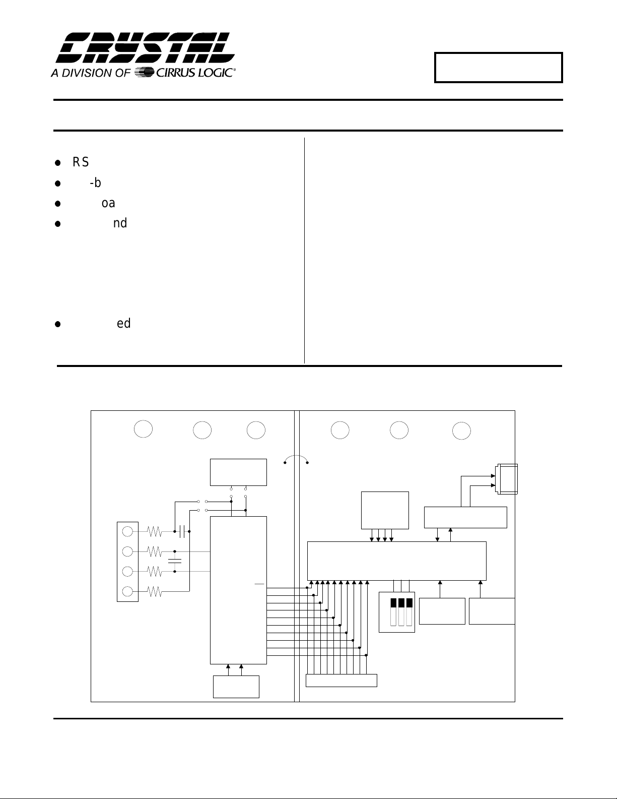
The CDB5529 is an inexpensive tool designed to evaluate the performance of the CS5529 16-bit Analog-toDigital Converter (ADC).
The evaluation board includes an LT1019 voltage reference, an 80C51 microcontroller, an RS232
driver/receiver, and firmware. The 8051 controls the serial communication between the evaluation board and
the PC via the firmware, thus, enabling quick and easy
access to all of the CS5529’s registers.
The CDB5529 also includes software for Time Domain
Analysis, Histogram Analysis, and Frequency Domain
Analysis.
ORDERING INFORMATION: CDB5529
+5/+2.5 ANALOG -2.5 ANALOG AGND DGND +5/3.3 DIGITAL
VOLTAGE
REFERENCE
J1
REF+
AIN+
AIN-
REF-
AIN+
AIN-
CRYSTAL
32768Hz
Cirrus Logic, Inc.
Crystal Semiconductor Products Division
P.O. Box 17847, Austin, Texas 78760
(512) 445 7222 FAX: (512) 445 7581
http://www.crystal.com
CS5529
CS
SDI
SDO
SCLK
D3
D2
D1
D0
A1
A0
XINXOUT
LEDs
80C51
MICROCONTROLLER
123
ON
OFF
TEST
SWITCHES
HDR6
Copyright Cirrus Logic, I nc. 1997
(All Rights Reserv ed)
+5 DIGITAL
RS232
CONNECTOR
RS232
DRIVER/RECEIVER
CRYSTAL
11.0592MHz
RESET
CIRCUITRY
AUG ‘97
DS246DB1
1
Page 2

CDB5529
PART I: HARDWARE
Introduction
The CDB5529 evaluation board provides a quick
means of testing the CS5529 Analog-to-Digital
Converter (ADC). The board interfaces the
TM
CS5529 to an IBM
RS-232 interface while operating from either a sin-
gle +5 V supply or dual ±2.5 volt supplies. To accomplish this, the board comes equipped with an
80C51 microcontroller and a 9-pin RS-232 cable
which physically interfaces the evaluation board to
the PC. Additionally, analysis software provides
easy access to the internal registers of the converter, and provides a means to display the converter’s
time domain, frequency domain, and noise histogram performance. The evaluation board’s software includes debug algorithms to trouble shoot
the evaluation board. Refer to the Trouble Shoot -
ing the Evaluation Board section for more details.
compatible PC via an
The evaluation board provides two voltage reference options, on-board and external. With HDR5’s
jumpers in positions 1 and 4, the LT1019 provides
an absolute voltage level of 2. 5 volts (the LT1019
was chosen for its low drift, typically 5ppm/°C). By
setting HDR5’s jumpers to position 2 and 3, the
user can supply an external voltage reference to
J1’s REF+ and REF- inputs (Application Note 4 on
Crystal Semiconductor’s web site details various
voltage references).
TM
The ADC serial interface is SPI
TM
MICROWIRE
lines (CS
the 80C51 microcontroller via port one. To interface an external microcontroller, these control lines
are also connected to HDR6. However to accomplish this, the evaluation board must be modified in
one of three ways: 1) cut the interface control traces
going to the microcontroller, 2) remove resistors
R1-R8, or 3) remove the microcontroller.
, SDI, SDO, and SCLK) are connected to
compatible. The interface co ntrol
and
Evaluation Board Overview
The board is partitioned into two sections: analog
and digital. The analog section consists of the
CS5529 and a precision voltage reference. The digital section consists of the 80C51 microcontroller,
the hardware test switches, the reset circuitry, and
the RS-232 interface.
The CS5529 is designed to digitize signals while
operating from a 32.768 KHz crystal. As shown in
Figure 1, a signal can be connected to the converter’s inputs via J1’s AIN+ and AIN- inputs. Note
that a simple RC network filters the input to reduce
broadband noise.
Figure 2 illustrates the schematic of the digital section. It contains the microcontroller, a Motorola
MC145407 interface chip, and test swit ches. The
test switches aid in debugging communication
problems between the CDB5529 and the PC. The
microcontroller derives its clock from an 11.0592
MHz crystal. From this, the controller is configured
to communicate via RS-232 at 9600 baud, no parity, 8-bit data, and 1 stop bit.
2 DS246DB1
Page 3
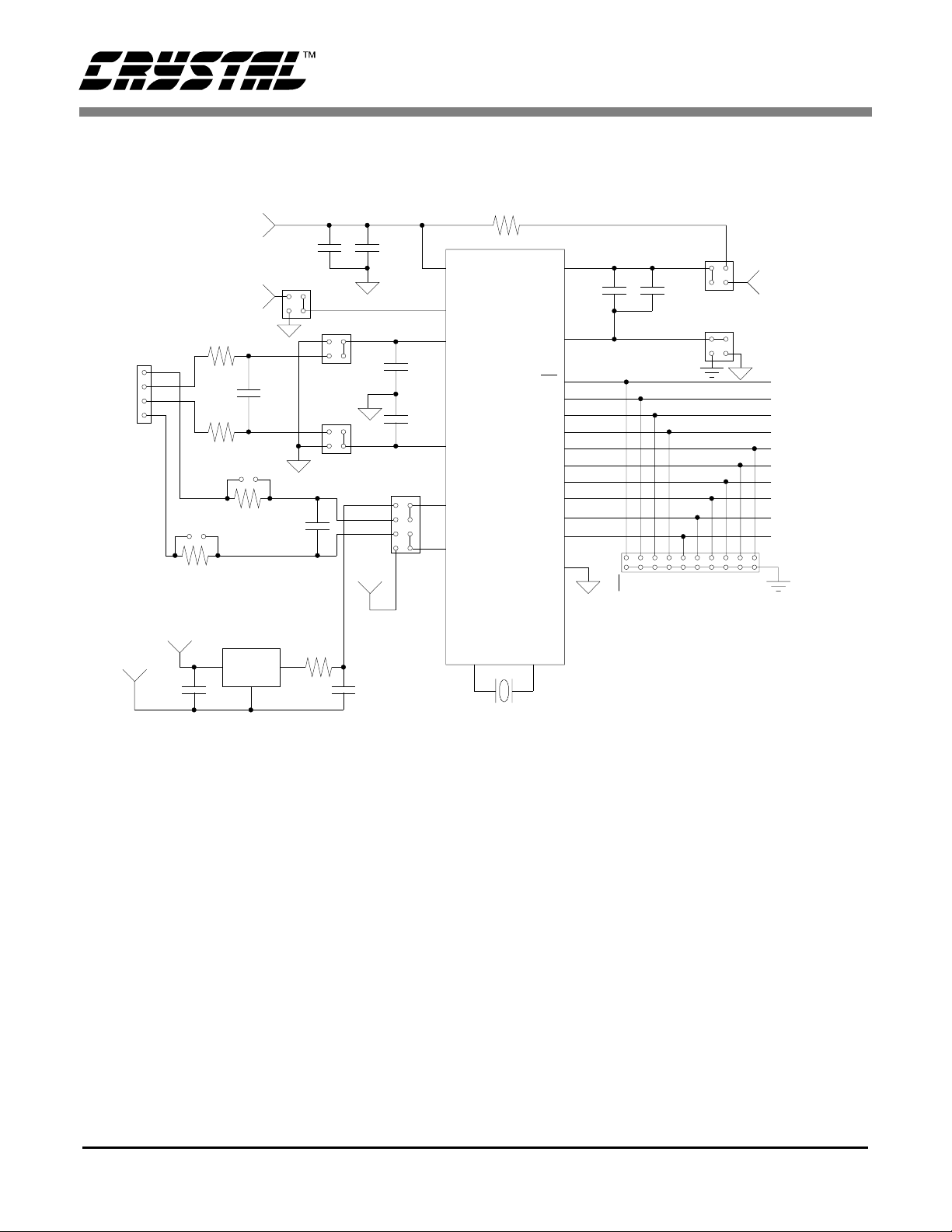
REF+
AIN+
AIN-
REF-
+5V / 2.5V Analog
-2.5V Analog
J1
JP4
R16
Ω
301
R18
301
R17
301
Ω
Ω
JP3
R15
301
0.1µF
HDR8
C2
4700pF
Ω
4700pF
C16
C1
HDR1
7
HDR2
1, AGND
2, AIN+
1, AIN2, AGND
1,LT1019
2,REF+
3,REF4,VA-
VA-
C30
10µF
0.68µF
HDR5
C3
0.68µF
C4
20
19
2
1
3
4
VA+
VAAIN+
AIN-
REF+
REF-
R21
Ω
10
U4
CS5529
VD+
DGND
CS
SDI
SDO
SCLK
D3
D2
D1
D0
A1
A0
DGND
13
C31
10µF
8
15
14
9
18
17
16
7
6
5
12
CS
CDB5529
HDR3
HDR9
D0D1D2
D3
+5V / 3.3V Digital
To
Figure 2
HDR6
C11
0.1µF
A1
A0
SDI
SDO
SCLK
+5V / 2.5V Analog
VA-
C21
0.1µF
U3
LT1019
2.5V
R22
50
Ω
C15
0.1µF
XOUT
10
Y2
32768Hz
Figure 1. Analog Schematic Section
XIN
11
DS246DB1 3
Page 4
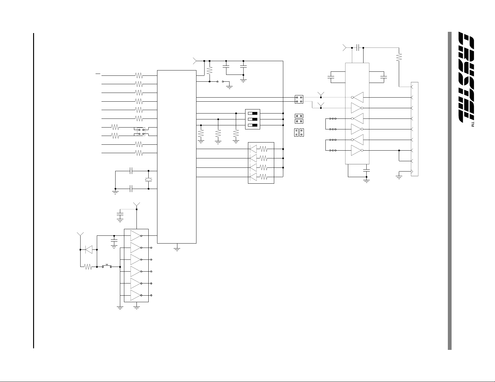
4 DS246DB1
From
Figure 1
+5V Digital
1N4148
750k
C26
10µF
VCC VDD
3
C2-
1
C2+
MC145407
2
+
R14
Ω
C25
10µF
10k
TXD
RXD
RTS
CTS
DTR
DSR
DCD
J2
RI
9
3
2
7
8
4
6
1
5
17
18
C1-
+
20
C1+
5
6
7
8
9
10
U1
4
C28
10µF
+
CDB5529
+5V Digital
+5V Digital
1
HDR10
Ω
Ω
Y1
+5V Digital
C19
1 2
3 4
5
9
11
13
14
17
R1
Ω
200
R2
Ω
200
R3
Ω
200
R4
Ω
200
R5
Ω
200
R6
Ω
200
R19
Ω
200
R20
Ω
200
6
8
10
12
U5
SN74HC14N
2
3
4
5
6
7
8
18
19
9
TP65
TP64
TP63
TP62
TP61
P1.0
P1.1
P1.2
P1.3
P1.4
P1.5
P1.6
P1.7
P3.5
P3.6
XTAL1
XTAL2
RST
UM1
80C51
VSS
20
CS
SDI
SDO
SCLK
D1
D0
Bypass
Cap
C18
R7
200
R8
200
C23
33pF
C0G
11.0592MHz
C24
33pF
C0G
0.1µF
A1
A0
D2
D3
D4
0.1µF
R9
RESET
Ω
VDD
P0.0
P3.0
P3.1
P3.2
P3.3
P3.4
P2.0
P2.1
P2.2
P2.3
40
39
10
11
12
13
14
5.11k
21
22
23
24
R12
10k
Ω
R13
Ω
JP2
+
R11
5.11k
C7
47µF
Ω
C17
0.1µF
R10
Ω
5.11k
6
5
LED_555_5003
S1
Test Switch 1
Test Switch 2
Test Switch 3
+18
+27
+3
+4
D1
HDR7
From RS-232
To RS-232
RESET
COMM
GAINCAL
OFFSETCAL
Normal
Loopback
C27
10µF
RXD
TP71
TXD
TP721615
+
14
13
12
11
Figure 2. Digital Schematic Section
Page 5
Register Read Command Byte Write Command Byte
Offset Register 0x90 (H) 0x80 (H)
Gain Register 0x92 (H) 0x82 (H)
Configuration Register 0x94 (H) 0x84 (H)
Conversion Data Register 0x96 (H) ---
Table 1. Microcontroller Command via RS-232
CDB5529
Table 1 lists the RS-232 commands used to communicate between the PC and the microcontroller.
To develop additional code to communicate to the
evaluation board via RS-232, the following applies: to write to an internal A DC register, choos e
the appropriate write command byte (See Table 1),
and transmit it LSB first. Then, transmit the three
data bytes, lowest order byte (bit s 7-0) first, with
the LSB of each byte transmitted first. These three
data bytes provide the 24-bits of information to be
written to the desired register. To read from an internal register, choose the appropriate read command byte and transmit it LSB first. Then, the
microcontroller automatically acquires the ADC’s
register contents and returns the 24-bits of information. The returned data is transmitted lowest order
byte first with the LSB of each byte transmitted
first.
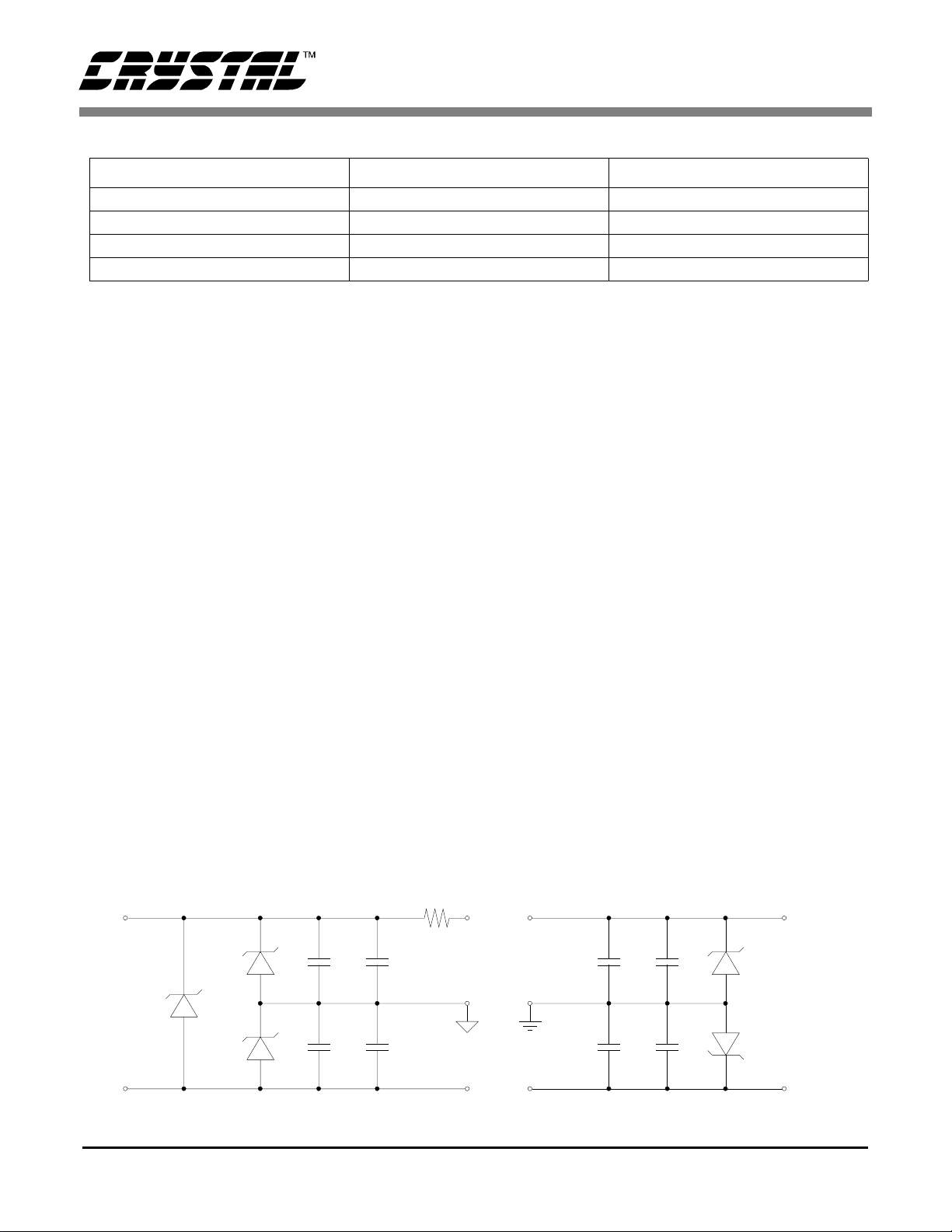
The CS5529 A/D converter is designed t o operate
from a single +5V or a dual ±2. 5V analog supply.
Figure 3 illustrates the power supply connections to
the evaluation board. The +2.5/5V Analog supplies
the positive analog section of the evaluation board,
the LT1019 and the ADC. The -2.5V Analog supplies the negative. HDR8 (see Figure 1) can be used
to bypass VA- to ground. The +5V Digital supplies
the digital section of the evaluation board. It powers the 80C51, the reset circuitry, and the RS-232
interface circuitry.
Using the Evaluation Board
The CS5529 is a highly integrated ADC. It contains
coarse/fine charge buffers and programmable output word rates (OWR). The buffers provide charge
to the modulator reducing the dynamic current demand from the signal being digitized and from the
external reference. The ADC’s digital filter allows
the user to select output word rates (OWR’s) from
1.88 Hz up to 101.1 Hz (assum ing a 32.768 kHz
clock). 303 Hz output word rates can be attained
when a 100kHz clock source is used. Since the
CS5529 has such a high degree of integration and
flexibility, the CS5529 data sheet should be read
thoroughly before and consulted during the use of
the CDB5529.
+2.5V / 5V Analog
Z2
P6KE6V8P
Z5
P6KE6V8P
-2.5V Analog
DS246DB1 5
Z3
P6KE6V8P
C6
47µF
+
C5
47µF
+
C20
0.1µF
C14
0.1µF
Figure 3. Power Supplies
R21
Ω
10
AGND
To HDR8
To HDR3
To µC VD+
DGND
C12
0.1µF
C12
0.1µF
C8
47µF
+
C8
47µF
+
+5V / 3.3V A/D Digital
Z4
P6KE6V8P
Z1
P6KE6V8P
+5V Digital
Page 6
CDB5529
Name Function Description
HDR1 Used to switch AIN+ between J1 input
and AGND.
HDR2 Used to switch AIN- between J1 input
and AGND.
HDR3 Used to switch digital power for the
converter (VD+) from positive analog
supply header (+5V/2.5V Analog) to
the positive digital supply header
(+5V/3.3V Digital).
HDR4 Does not exist.
HDR5 Used to switch VREF+ and VREF-
pins from external J1 connection
header to the on board LT1019 refer-
ence.
HDR6 Used to connect external micro-con-
troller.
HDR7 Used in conjunction with the self test
modes to test the UART communica-
tion between the microcontroller and
the PC.
HDR8 Used to switch the analog compo-
nent’s (LT1019 and converter) nega-
tive potential between the -2.5V
Analog header and AGND.
HDR9 Used in conjunction with HDR3 to
switch the digital ground of the con-
verter (DGND) from the AGND header
to the DGND header.
HDR10 Used to switch the A0 and A1 output
switches of the converter into the
microcontroller. These shunts must be
disconnected when the converter
powered from bipolar supplies.
Software
The evaluation board comes with software and an
RS-232 cable to link the evaluation board to the
PC. The executable software was developed with
TM
Lab Windows/CVI
TM
dows
3.1 or later. After installing the software,
read the readme.txt file for last minute changes in
the software. Additionally, Part II: Software further details how to install and use the software.
IBM, AT and PS/2 are trademarks of International Business Machines Corporation.
Windows is a trademark of Microsoft Corporation.
Lab Windows and CVI are trademarks of National
Instruments.
SPI is a trademark of Motorola.
MICROWIRE is a trademark of National Semiconduc-
tor.
and meant to run under Win-
6 DS246DB1
Page 7

CDB5529
PART II: SOFTWARE
Installation Procedure
To install the software:
1) Turn on the PC.
2) At DOS prompt type WIN to Launch Windows 3.1
3) Insert the Installation Diskette into the PC.
4) From within the Windows Program Manager,
pull down File from the menu bar and select
the Run option.
5) At the prompt
type: A:\SETUP.EXE <enter>.
6) The program will begin installation.
7)After a few seconds, the user will be
prompted to enter the directory in which to
install the CVI Run-Time Engine
Run-Time Engine
created with Lab Windows/CVI
approximately 1.5 megabytes of hard drive
space. If the default directory is acceptable,
select OK and the Run-Time Engine
be installed there.
8) After the Run-Time Engine
user is prompted to enter the directory in
which to install the CDB5529 software.
Select OK to accept the default directory.
9)The program takes a few minutes to install.
After the program is installed, double click on
the Eval5529 icon to launch it. After a few
seconds, the user should be in the graphical
user interface environment.
Note: The software is written to run with 640 x 480
(standard VGA in Windows 3.1
it will work with 1024 x 768 resolution. If the user interface seems to be a little small, the user might consider
setting the display settings to the 640 x 480 standard
(640x480 was chosen to accommodate a variety of
computers).
TM
or later.
TM
. The
TM
manages executables
TM
and takes
TM
TM
is installed, the
TM
) resolution; however,
will
Using the Software
At start-up, the window START-UP CONFIGURATION appears first. This window contains in-
formation concerning the software’s ti tle, revision
number, copyright date, etc. Additionally, at the
top of the screen is a menu bar which displays user
options. Notice, the men u bar item Menu is initially
disabled. This eliminates any conflicts with the
mouse or concurrent use of modems. Before proceeding any further, the user is prompted to select
the serial communication port. To initialize a p ort,
pull down option Setup from the m enu bar and select either COM1 or COM2. Next, select the appropriate part under the Part menu. After a port is
initialized and the part selected, it is a good idea to
test the RS-232 link between the PC and the evaluation board. To do this, pull down th e S etup menu
from the menu bar and select the option
TESTRS232. The user is then prompted to set the
evaluation board’s test switches to 011 and then reset the board. Once this is done, proceed with the
test. If the test fails, check the hardware connection
and repeat again. Otherwise, set the test switches to
000 (normal mode) and reset the board. The option
Menu is now availabl e and performance tests can
be executed.
The evaluation software provides three types of
analysis tests - Time Domain, Frequency Domain,
and Histogram. The Time Domain analysis processes acquired conversions to produce a plot of
Conversion Sample Number versus Magnitude.
The Frequency Domain analysis processes acquired conversions to produce a magnitude versus
frequency plot using the Fast-Fourier transform
(results up to Fs/2 are calculated and plotted). Also,
statistical noise calculations are calculated and displayed. The Histogram analysis processes acquired conversions to produce a histogram plot.
Statistical noise calculations are also calculated and
displayed (see figures 4 through figure 9).
DS246DB1 7
Page 8

CDB5529
The evaluation software was developed with L ab
TM
Windows/CVI
from National Instruments. More sophisticated
analysis software can be developed by purchasing
the development package from National Instruments (512-794-0100).
, a software development package
Menu Bars Overview
The menu bar controls the link bet ween windows
and allows the user to exit the program. It also allows the user to initialize the serial port and load
presaved data conversions from a file. The five
principal windows are the START UP CONFIGURATION (also referred to as the Setup Window),
the Input / Output Window, the Histogram Window, the Power Spectrum Window (also referred to
as the FFT window), and the Time Domain Window.
Specifically, the menu bar has the following control items:
Menu: To select, click on option Menu from the
menu bar, or use associated hot keys . The items associated with MENU are listed and described below.
Setup Window (F1)
Input/Output Window (F2)
Histogram Window (F3)
Power Spectrum Window (F4)
Time Domain Window (F5)
These five menu items allow the user to navigate
between the five windows. They are available at all
times via the menu bar or hot keys.
SETUP: To select, click on option Setup from the
menu bar. The functions available under Setup are:
COM1: When selected, COM1 is initialized to
9600 baud, no parity, 8 data bits, and 1 stop bit.
COM2: When selected, COM2 is initialized to
9600 baud, no parity, 8 data bits, and 1 stop bit.
Load From Disk: Used to load and display previously saved data conversions from a file. The fi le
must comply with the CDBCAPTURE file save
format. The format is: part number, number of bits,
number of conversions, maximum range, and the
data conversions. The user is prompted to enter the
path and file name of previously saved data. To
prevent hardware conflicts, this option is deactivated while in the Input/Output Window.
TESTRS232: This test mode tests the ability of th e
PC to communicate to the evaluation board. It consists of two subt ests: 1) test the link between t he
PC and the RS-232 interface circuitry; and 2) test
the RS-232 link between the PC and the microcontroller. HDR7 distinguishes these two subtests. Set
HDR7 to N ormal to tes t the complete communication link. Or set HDR7 to Loop Back to test the link
between the RS-232 Circuitry and the PC. Then,
set the test switches to 110 and reset the evaluation
board. The LED’s should indicate a binary six signifying that the hardware is ready to initiate the
test. To complete the tes t, the user must initialize
the PC. First, use the SETUP menu to select a communications port and then select the TESTRS232
option. From there, prompts navigate the user
through the test. The PC indicates if the test passes
or fails. Once either test is complete, the LED’s
toggle to indicate that the test mode is complete.
QUIT: Allows user to exit program .
Input/Output Window Overview
The Input/Output Window al lows the user to read
and write to the internal register of the converter in
either binary or hexadecimal, and acquire real-time
conversions. It has quick access control icons that
quickly reset the converter, reset the converter’s serial port, or self-calibrate the converter’s offset and
gain. The following are controls and indicators associated with this window.
Acquire: This is a control icon. When pressed, the
PC transmits the collect single conversion command
8 DS246DB1
Page 9

CDB5529
to the microcontroller. The microcontroller in turn
collects a conversion from the ADC and returns it to
the PC. The PC stores the conversion and collects
additional conversions to form a set. From the sample set collected, the high, the low, peak-to-peak, av erage, and standard deviation, are computed (the
size of the data set is set by the Num To Average input) and then the display icons are updated. This
process continues until the STOP button is pressed,
or until another window is selected. Note: The
quick access control icons are disabled once Acquire
is selected. This eliminates potential hardware conflicts.
BINARY: Input icons set or clear the 24 individual
bits in the gain, configuration, or offset registers.
The bits are first set, then the control icon Write All
Registers is selected to update the registers in the
converter.
CONFIGURATION REGISTER: Text display
box that displays the decoded meaning of each bit
in the configuration register.
DECIMAL: Three display icons that display in
decimal the contents of the gain, configuration, and
offset registers.
DIGITAL OUTPUT: Display icon that displays
the six states of the output latch. A0 and A1 are invalid when the converter is powered from bipolar
supplies.
GAIN REGISTER: Display icon that displays the
decimal equivalent of the bits set in gain register.
HEX: Three input/display icons that allow a user to
set the 24 bits in the gain, configuration, or offset
registers via 6 hexadecimal nibbles. If the upper
nibbles in the registers are zero’s, then leading zero
nibbles need to be entered.
Num To Average: Input icon that sets the size of
the data conversion set referred to when the Acquire button is pressed.
Read All Registers: This is a control icon. When
pressed the gain, offset, and configuration registers
contents are acquired. Then, the configuration text
box and the register content icons are updated.
Reinitialize: This is a control icon. When pressed,
128 logic 1’s followed by a logic ‘0’ are sent to the
ADC’s serial port to reset its port. It does not reset
the RS-232 link.
Reset A/D: This is a control icon. When pres sed,
the microcontroller sends the appropriate commands to return the converter to its initial default
state.
SELF Calibrate: This is a control icon. When
pressed, the appropriate c om m ands a re se nt t o t he
ADC to calibrate its own offset and gain.
STOP: Stops the collection of conversion data.
Write All Registers: This is a control icon. When
pressed, the 72 binary input icons settings are acquired. This data is then transmitted to the ADC’s
gain, offset, and configuration registers. Then, the
PC’s display is updated to reflect the registers
changes.
DS246DB1 9
Page 10

CDB5529
Histogram Window Overview
The following is a description of the controls and indicators associated with the Histogram Window.
Many of the control icons are usable from the Histogram Window, the Frequency Domain Window, and
the Time Domain Window. For brevity, they are
only described in this section.
BIN: Displays the x-axis value of the cursor on the
Histogram.
CANCEL: Once selected, it allow s a user to exit
from the COLLECT algorithm. If data co nversion
sample sets larger than 64 are being collected and
the CANCEL button is selected, it is recommended
that the user reset th e evaluation board. The board
will eventually recover from the continuous collection mode, but the recovery time could be as long
as 10 minutes.
COLLECT: Initiates the data conversion collection process. COLLECT has tw o modes of ope ration: collect from file or collect from converter. To
collect from a file an appropriate file from the SETUP-DISK menu bar option must be selected. Once
a file is selected, its content is displayed in the
graph. If the user is collecting real-time conversions to analyze, the appropriate COM port must be
selected. The user is then free to collect the preset
number of conversions (preset by the CONFIG
pop-up menu discussed below). Notice, there is a
significant acquisition time difference in the two
methods.
ie and 7-term Hodie are windowing algorithms developed at Crystal Semiconductor. If information
concerning these algorithms is needed, call technical support.
AVERAGE: Sets the number of consecutive FFT ’s
to perform and average.
LIMITED NOISE BANDWIDTH: Limits the
amount of noise i n the convert ers bandwidth. Default is 0 Hz.
OK: Accept the change
MAGNITUDE: Displays the y-axis value of the
cursor on the Histogram.
MAXIMUM: Indicator for the maximum value of
the collected data set.
MEAN: Indicator for the mean of the data sample set.
MINIMUM: Indicator for the minimum value of
the collected data set.
OUTPUT: Control that calls a pop-up menu. This
menu controls three options: 1) save current data
set to a file with the CDBCAPTURE format, 2)
print current screen, or 3) print current graph.
RESTORE: Restores the display of the graph after
zoom has been entered.
STD. DEV.: Indicator for the Standard Deviation
of the collected data set.
TEST: Quick access control icon, similar to the hot
keys, to allow user to quickly switch between a time
domain, a frequency domain, or a histogram display.
CONFIG: Opens a pop-up panel to configure how
much data is to be collected, and how to pr ocess the
data once it is collected. The following are controls
and indicators associated with the CONFIG panel.
SAMPLES: User selection of 64, 256, 512, 1024,
2048, 4096, or 8192 conversions.
WINDOW: Used in the Power Spectrum Window
to calculate the FFT. Windowing algorithms include the Blackman, Blackman-Harris, Hanning,
5-term Hodie, and 7-term Hodie. The 5-term Hod-
10 DS246DB1
VARIANCE: Indicates the Variance for the current data set.
ZOOM: Control icon that allows the operator to
zoom in on a specific portion of the current graph.
To zoom, click on the ZOOM icon, then click on the
graph to select the first point (the 1st point is the top
left corner of the zoom box). Then click on the
graph again to select the second point (the 2nd point
is the bottom right corner of the zoom box). Once an
area has been zoomed in to, the OUTPUT functions
Page 11

CDB5529
can be used to print a hard copy of that region. Click
on RESTORE when done with the zoom function.
Frequency Domain Window (i.e. FFT)
The following describe the controls and indicators
associated with the Frequency Domain Window.
CANCEL: See description in Histogram Window
Overview.
COLLECT: See description in Histogram Win-
dow Overview.
CONFIG: See description in Histogram Window
Overview.
FREQUENCY: Displays the x-axis value of the
cursor on the FFT display.
MAGNITUDE: Displays the y-axis value of the
cursor on the FFT display.
OUTPUT: See description in Histogram Window
Overview.
ZOOM: See description in Histogram Window
Overview.
# of AVG: Displays the number of FFT’s averaged
in the current display.
Time Domain Window Overview
The following controls and indicators are associated with the Time Domain Window.
CANCEL: See description i n Histogram Window
Overview.
COLLECT: See description in Histogram Win-
dow Overview.
CONFIG: See description in Histogram Window
Overview.
COUNT: Displays current x-position of the cursor
on the time domain display.
MAGNITUDE: Displays current y-position of the
cursor on the time domain display.
S/D: Indicator for the Signal-to-Distortion Ratio, 4
harmonics are used in the calculations (decibels ) .
S/N+D: Indicator for the Signal-to-Noise + Distortion Ratio (decibels).
SNR: Indicator for the Signal-to-Noise Ratio, first
4 harmonics are not included (decibels).
S/PN: Indicator for the Signal-to-Peak Noise Ratio
(decibels).
TEST: See description in Histogram Window
Overview.
MAXIMUM: Indicator for the maximum value of
the collected data set.
MINIMUM: Indicator for the minimum value of
the collected data set.
OUTPUT: See description in Histogram Window
Overview.
TEST: See description in Histogram Window
Overview.
ZOOM: See description in Histogram Window
Overview.
DS246DB1 11
Page 12

CDB5529
Trouble Shooting the Evaluation Board
This section describes special test modes incorporated
in the microcontroller software to diagnose hardware
problems with the evaluation board.
Note: To enter these modes, set the test switches to the
appropriate positi on an d reset the eval uation board . To re enter t he no rmal opera tion mod e, set t he s wi tches b ack to
binary zero and r eset the boar d aga in.
Test Mode 0, Normal Mode: This is the default
mode of operation. To en ter th is mo d e, set th e test
switches to 000 and reset the board. The evaluation
board allows normal read/writes to the ADC’s registers. All the LED’s toggle on then off after reset,
and then only when communicating with th e PC.
Test Mode 1, Loop Back Test: This test mode
checks the microcontroller’s on-chip UART. To
enter this mode, set test switches to 001, set HDR7
for loop back, and then reset the board. If the communication works, all the LED's toggle. Otherwise, only 1/2 of the LED’s toggle to indicate a
communication problem.
Test Mode 2, Read/Write to ADC: This test mode
tests the microcontroller’s ability to read and write
to the ADC. To enter this mode, set the switches to
010 and reset the board. In this test mode, the
ADC’s configuration, offset, and gain registers are
written to and then read from. If the correct data is
read back, all the LED's toggle. Otherwise, only
half of them toggle to indicate an error.
Test Mode 3, Continuously Acquire Single Conversion: This test mode repetitively acquires a sin-
gle conversion. To enter this mode, set the test
switches to 011 and press reset. A binary three is indicated on the LED’s. By probing HDR6 and using
as a triggering pin, an oscilloscope or logic an-
CS
alyzer will display in real-time how the microcontroller reads conversion data.
Test Mode 4: Reserved for future modifications.
Test Mode 5, Continuously Read Gain Register:
This test mode repetitively acquires the gain registers default contents (0x400000 HEX). To enter
this mode, set the test switches to 101 and press reset. The LED’s should indicate a binary five. By
probing HDR6 and using CS
as a triggering pin, an
oscilloscope or logic analyzer will display in realtime how the microcontroller acquires a conversion.
Test Mode 6, PC to Microcontroller RS-232
Communication Link Test: This test mode tests
the ability of the PC to communicate to the evaluation board. It consists of two subtests: 1) test the
link between the PC and the RS-232 interface circuitry; and 2) test the RS-232 link between the PC
and the microcontroller. HDR7 distinguishes these
two subtests. Set HDR7 to Normal to test the complete communication link. Or set HDR7 to Loop
Back to test the link between the RS-232 Circuitry
and the PC. Then, set the test switches to 110 and
reset the evaluation board. The LED’s should indicate a binary six signifying that the hardware is
ready to initiate the tes t. To complete the test, the
user must initialize the PC. First, use th e SETUP
menu to select a communications port and then select the TESTRS232 option. From there, user
prompts navigate the user through the test. The PC
indicates if the test passes or fails. Once either test
is complete, the LED’s toggle to indicate that the
test mode is complete.
Test Mode 7, Toggle LED’s: This test mode tests
the evaluation board LED’s. To enter this mode,
set the test switches to 111 and reset the board. If
the mode passes, the LED ’s toggle.
Note: Remember, to return to the normal operating
mode, set the test switche s to binar y zero, return HDR7
to Normal, and reset the evaluation board.
12 DS246DB1
Page 13

CDB5529
Figure 4. Main Menu
Figure 5. Input/Output Window
DS246DB1 13
Page 14

CDB5529
Figure 6. Frequency Domain Analysis
Figure 7. Configuration Menu
14 DS246DB1
Page 15

CDB5529
Figure 8. Time Domain Analysis
Figure 9. Histogram Analysis
DS246DB1 15
Page 16
CDB5529
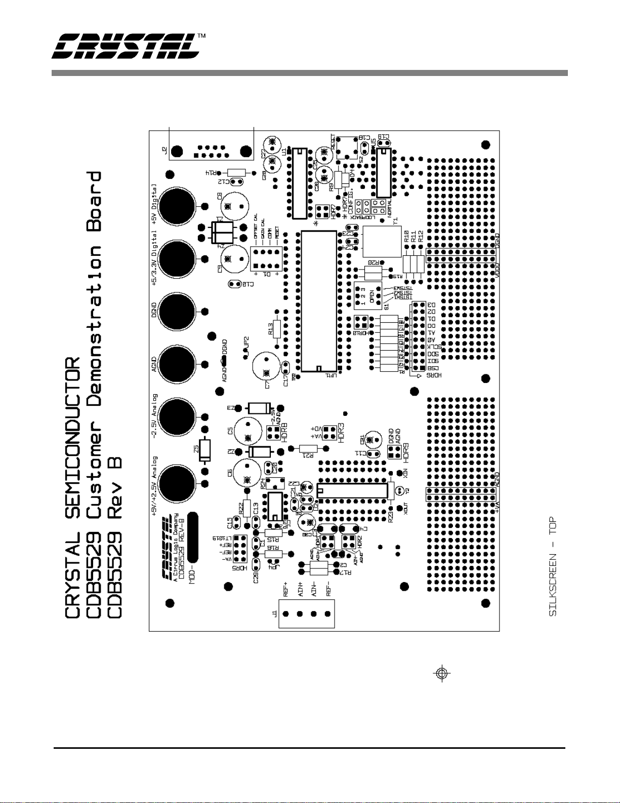
Figure 10. CDB5529 Component Side Silkscreen
16 DS246DB1
Page 17
CDB5529
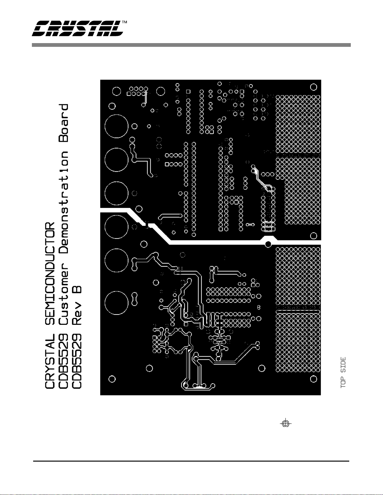
Figure 11. CDB5529 Component Side (top)
DS246DB1 17
Page 18

CDB5529
Figure 12. CDB5529 Solder Side (bottom)
18 DS246DB1
Page 19

• Notes •
Page 20

 Loading...