

Page 1
\
CDB5521/22/23/24/28
CDB5521/22/23/24/28 Evaluation Board and Software
Features
l Evaluation Board and Software Supports All
Chips: CS5521, CS5522, CS5523, CS5524,
and CS5528
l Direct Thermocouple Interface
l RS-232 to PC With Test Modes
l On-board 80C51 Micr ocontroller
l On-board Voltage Reference
l Lab Windows/CVI
– Register Setup & Chip Control
– Data Capture
– FFT Analysis
– Time Domain Analysis
– Noise Histogram Analysis
l On-board Charge Pump Drive Circuitry
REF+
TM
Evaluation Software
+5 ANALOG-5 ANALOG AGND
VOLTAGE
REFERENCE
J2
General Description
The CDB5521/22/23/24/28 is an inexpensive tool designed to evaluate the performance of the CS5521,
CS5522, CS5523, CS5524, and CS5528 Analog-to-Digital Converters (ADC).
The evaluation board includes a 2.5 V voltage reference,
an 80C51 microcontroller, an RS232 driver/receiver, and
firmware. The 8051 controls the serial communication
between the evaluat ion board and the PC vi a the firmware, thus, enabling qui ck and ea sy ac cess to all of th e
CS5521/22/23/24/28’s registers.
The CDB5521/22/23/24/28 also includes one installed
ADC sample, and software for Dat a Capture, Time Domain Analysis, Histogram Analysis, and Frequency
Domain Analysis.
ORDERING INFORMATION
CDB5521/22/23/24/28 Evaluation Board
DGND
+5 DIGITAL
REF-
J1
AIN1+
AIN1-
AIN2+
AIN2-
AIN3+
AIN3-
AIN4+
AIN4-
NBV DRIVE
CIRCUITRY
NBV
CPD
CS5521
CS5522
CS5523
CS5524
CS5528
CRYSTAL
32.768 kHz
Preliminary Product Information
P.O. Box 17847, Austin, Texas 78760
(512) 445 7222 FAX: (512) 445 7581
http://www.cirrus.com
TEST
SWITCHES
on off
3
2
1
DRIVER/RECEIVER
RESET
CIRCUITRY
CONNECTOR
RS232
CS
SDI
SDO
SCLK
LEDs
A0
A1
80C51
Microcontroller
CRYSTAL
11.0592 MHz
This document contains information for a new product.
Cirrus Logic reserves the right to modify this product without notice.
Copyright Cirrus Logic, Inc. 2000
(All Rights Reserved)
RS232
MAY ‘00
DS317DB2
1
Page 2

TABLE OF CONTENTS
1. PART I: HARDWARE ............................................................................................................... 4
1.1 Introduction ........................................................................................................................4
1.3 Using the Evaluation Board ............................................................................................... 8
1.4. Power Connections ........................................................................................................... 8
1.5 Negative Bias Voltage ........................................................................................................ 8
1.6 Software ............................................................................................................................. 9
1.7. Writing Your Own Interface Software ................................................................................ 9
2. PART II: SOFTWARE ............................................................................................................. 13
2.1 Installation Procedure ......................................................................................................13
2.3 Menu Bars Overview ........................................................................................................ 14
2.4 Setup Window Overview ..................................................................................................15
2.5 Data FIFO Window Overview .......................................................................................... 15
2.6 Histogram Window Overview ...........................................................................................16
2.7 Frequency Domain Window (i.e. FFT) ............................................................................. 17
2.8 Time Domain Window Overview ......................................................................................18
2.9 Calibration Window Overview ..........................................................................................19
2.10 Trouble Shooting the Evaluation Board ......................................................................... 19
LIST OF FIGURES
CDB5521/22/23/24/28
Figure 1. CS5522 Analog Section................................................................................................... 5
Figure 2. CS5524/28 Analog Section..............................................................................................6
Figure 3. Digital Section .................................................................................................................. 7
Figure 4. Power Supplies ................................................................................................................ 8
Figure 5. Main Menu .....................................................................................................................21
Figure 6. Setup Window................................................................................................................ 21
Figure 7. Data FIFO Window.........................................................................................................22
Figure 8. Frequency Domain Analysis ..........................................................................................22
Figure 9. Calibration Menu............................................................................................................ 23
Figure 10. Time Domain Analysis .................................................................................................23
Figure 11. Histogram Analysis (Using the CS5524 with default register settings and
24-bit output words) ...................................................................................................... 24
Figure 12. CDB5521/22/23/24/28 Component Side Silkscreen....................................................25
Contacting Cirrus Logic Support
For a complete listing of Direct Sales, Distributor, and Sales Representative contacts, visit the Cirrus Logic web site at:
http://www.cirrus.com/corporate/contacts/
IBM, AT and PS/2 are trademarks of International Business Machines Corporation.
Windows is a trademark of Microsoft Corporation.
Lab Windows and CVI are trademarks of National Instruments.
TM
SPI
is a trademark of Motorola.
MICROWIRE
TM
is a trademark of National Semiconductor.
Preliminary product inf o rmation describes product s whi ch are in production, b ut f or which full character iza t i on da t a i s not yet available. Advance p rodu ct i nformation describes products which are in development and subject to development changes. Cirrus Logic, Inc. has made best efforts to ensure that the information
contained in this document i s accurat e and reli able. However , t he infor mation is subje ct to chang e without noti ce and is provi d ed “AS IS” without warrant y of
any kind (express or implied). No responsibility is assumed by Cirrus Logic, Inc. for the use of this information, nor for infringements of patents or other ri g ht s
of third parties. This document is the pro perty of Cirrus Logi c, Inc. and i mplie s no licen se under patents, copyrights, tr ademarks, or trade secre ts. No part of
this publication may be copied, reproduced , stored in a retrieval system, or transmitted, in any form or by any means (electro nic, mechanical, photographic, or
otherwise) without the pr i or writ ten consent of Cirrus Logic, Inc. It e ms f rom any Ci rrus Logic website or disk may be printed for use by the user. However, no
part of the printout or electronic files may be copied, reproduced, stored in a retrieval system, or transmitted, in any form or by any means (electronic, mechanical,
photographic, or otherwise) without the prior written consent of Cirrus Logic, Inc.Furthermore, no part of this publication may be used as a basis for manufacture
or sale of any items without the prior written consent of Cirrus Logic, Inc. The names of products of Cirrus Logic, Inc. or other vendors and suppliers appearing
in this document may be trademarks or service marks of their respective owners which may be registered in some jurisdictions. A list of Cirrus Logic, Inc. trademarks and service marks can be found at http://www.cirrus.com.
2 DS317DB2
Page 3

Figure 13. CDB5521/22/23/24/28 Component Side (top) ............................................................. 26
Figure 14. CDB5521/22/23/24/28 Solder Side (bottom) ............................................................... 27
LIST OF TABLES
Table 1. Header Descriptions.......................................................................................................... 9
Table 2. Microcontroller Read/Write Commands via RS-232 ....................................................... 10
Table 3. Microcontroller Conversion Commands via RS-232....................................................... 10
Table 4. Microcontroller Self Calibration Commands via RS-232................................................. 11
Table 5. Microcontroller System Calibration Commands via RS-232 ........................................... 12
CDB5521/22/23/24/28
DS317DB2 3
Page 4

CDB5521/22/23/24/28
1. PART I: HARDWARE
1.1 Introduction
The CDB5521/22/23/24/28 evaluation board provides a means of testing the CS5521/22/23/24/28
Analog-to-Digital Converters (ADCs). The board
interfaces the converters to an IBMTM compatible
PC via an RS-232 interface while operating from a
+5 V and -5 V power supply. To accomplish this,
the board comes equipped with an 80C51 microcontroller and a 9-pin RS-232 cable, which physically interfaces the evaluation board to the PC.
Additionally, analysis software provides easy access to the internal registers of the converters and
provides a means to capture data and display the
converters’ time domain, frequency domain, and
noise histogram performance.
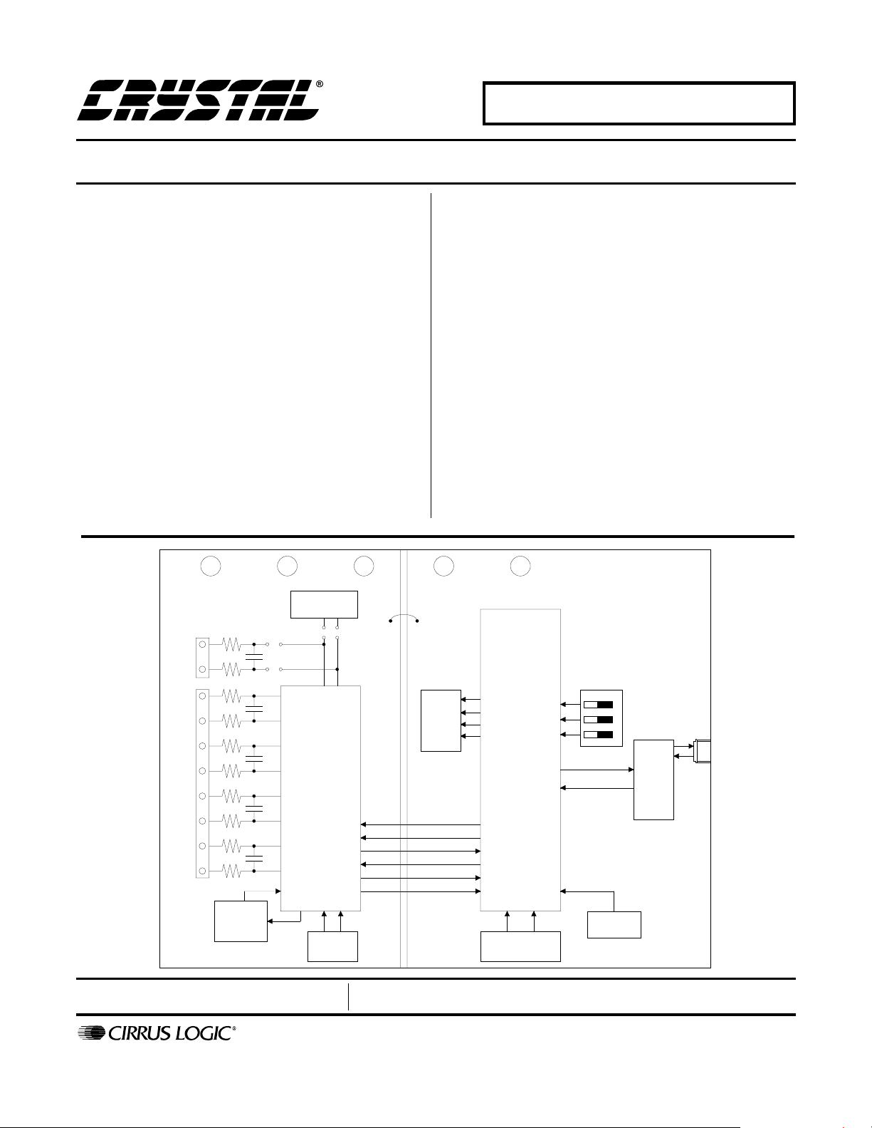
1.2 Evaluation Board Overview
The board is partitioned into two main sections: analog and digital. The analog section consists of the
either the CS5521, CS5522, CS5523, CS5524 or
CS5528, a precision voltage reference, and the circuitry to generate a negative voltage. The digital
section consists of the 80C51 microcontroller, the
hardware test switches, the reset circuitry, and the
RS-232 interface.
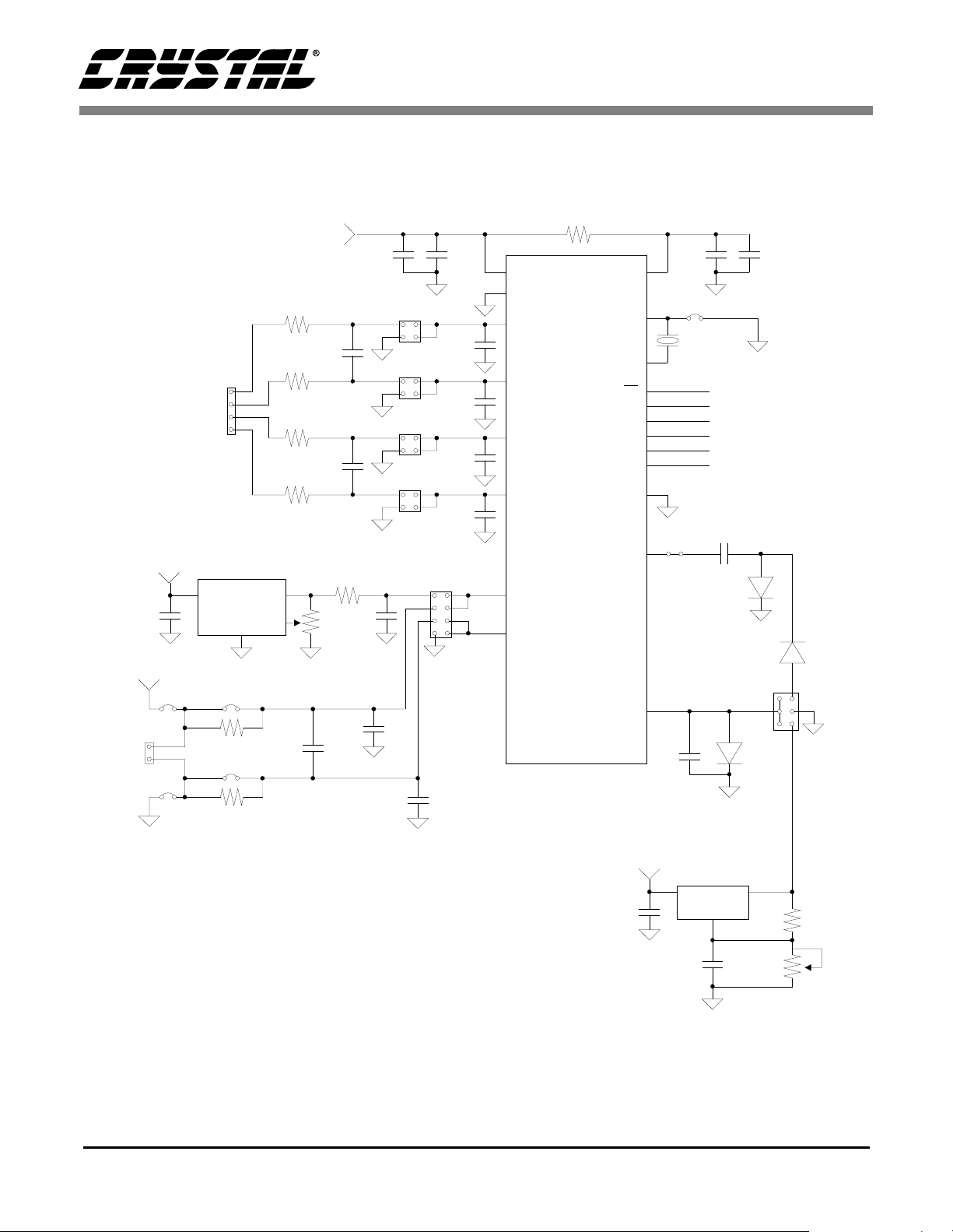
The CS5521/22/23/24/28 is designed to digitize
low level signals while operating from a
32.768 KHz crystal. As shown in Figures 1 and 2,
a thermocouple can be connected to the converter’s
inputs via J1’s AIN+ and AIN- inputs. Note, a simple RC network filters the thermocouple’s output to
reduce any interference picked up by the thermocouple leads.
The evaluation board provides two voltage reference options, on-board and external. With HDR5’s
jumpers in positions 1 and 4, the LT1019 provides
2.5 volts (the LT1019 was chosen for its low drift,
typically 5ppm/°C). By setting HDR5’s j umpers to
position 2 and 3, the user can supply an external
voltage reference to J2’s REF+ and REF- inputs
(Application Note 4 on the web details various
voltage references).
The A/D converters’ serial interfaces are SPI
and MICROWIRETM compatible. The interface
control lines (CS, SDI, SDO, and SCLK) are connected to the 80C51 microcontroller via port one.
To interface a different microcontroller to the ADC
chip, the control lines to the ADC are availa ble at
HDR6 (Header 6). However, to connect an external
microcontroller to the header, the evaluation board
must be modified in one of three ways: 1) cut the
interface control traces going to the on-board
80C51 microcontroller, 2) remove resistors R1-R6,
or 3) remove the 80C51 microcontroller from its
socket on the evaluation board.
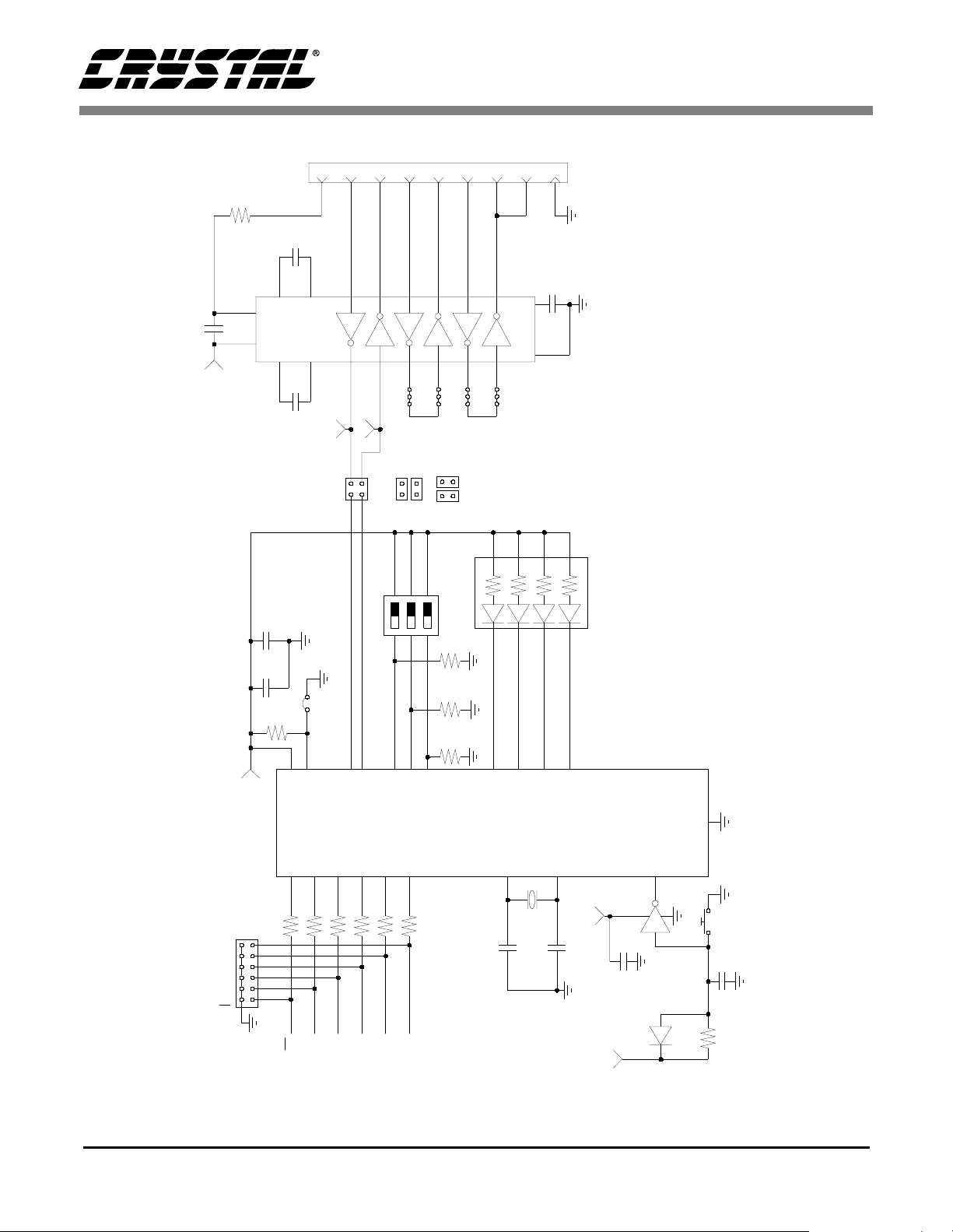
Figure 3 illustrates the schemati c of the digital section. It contains the microcontroller, a Motorola
MC145407 interface chip, and test switches. The
test switches aid in debugging communication
problems between the CDB5521/22/23/24/28 and
the PC. The microcontroller derives its clock from
an 11.0592 MHz crystal. From this, the controller
is configured to communicate via RS-232 at
9600 baud, no parity, 8-bit data, and 1 stop bit.
TM
4 DS317DB2
Page 5
+5V Analog
C20
0.1µF
+5V Analog
J2
REF+
REF-
JP6
JP5
AIN1+
AIN1-
AIN2+
AIN2-
R21
Ω
301
R22
Ω
301
J1
1
2
3
4
U4
LT1019
GND
JP3
JP4
OUTIN
TRIM
4700pF
+5V Analog
R17
C2
Ω
301
4700pF
R18
Ω
301
R25
C3
Ω
301
4700pF
R26
Ω
301
R7
20k
C1
R24
49.9
Ω
C41
0.1µF
0.1µF
Ω
C16
0.1µF
C14
C40
0.1µF
HDR1
HDR2
HDR8
HDR9
R15
10
Ω
C29
2
10µF
C32
0.1µF
C33
0.1µF
C34
0.1µF
C35
0.1µF
HDR5
1
3
4
VA+
AGND
AIN1+
AIN1-
U6
CS5521
VD+
XOUT
CS5522*
18
AIN2+
17
AIN2-
20
VREF+
19
VREF-
* CS5521 and CS5522 are interchangeable
SDO
SCLK
DGND
CPD
CDB5521/22/23/24/28
XIN
CS
SDI
A0
A1
NBV
14
10
11
9
8
12
15
6
16
13
7
5
C22
10µF
C30
10µF
JP7
Y2
32.768kHz
Figure 3
0.033µF
1N4148
+
C9
D2
To
D3
1N4148
CPD
GND
BAT85
C15
0.1µF
HDR4
337
D5
-5V Analog
C21
+
1µF
LM337_LZ
C11
0.1µF
U2
ADJ
VOUTVIN
R23
Ω
1k
+
R16
1k
Ω
Figure 1. CS5522 Analog Section
DS317DB2 5
Page 6

+5V Analog
C20
0.1µF
+5V Analog
REF+
REF-
CDB5521/22/23/24/28
R15
Ω
+5V Analog
C14
0.1µF
R17
C2
Ω
301
4700pF
R18
Ω
301
OUTIN
TRIM
R25
301
R26
301
R27
301
R28
301
R29
301
R30
301
C1
4700pF
Ω
4700pF
Ω
Ω
4700pF
Ω
Ω
4700pF
Ω
C3
C4
C31
20k
R24
49.9
R7
Ω
C41
0.1µF
0.1µF
J1
1
AIN1+
2
AIN1-
3
AIN2+
4
AIN2-
5
AIN3+
6
AIN3-
7
AIN4+
8
AIN4-
U4
LT1019
GND
R21
301
301
JP3
Ω
JP4
R22
Ω
JP6
J2
JP5
HDR1
HDR2
HDR8
HDR9
HDR11
HDR12
HDR13
HDR14
Ω
C16
C40
0.1µF
C29
2
10µF
C32
0.1µF
C33
0.1µF
C34
0.1µF
C35
0.1µF
C36
0.1µF
C37
0.1µF
C38
0.1µF
C39
0.1µF
HDR5
* CS5523, CS5524 and CS5528
are interchangeable
VA+
1
AGND
3
AIN1+/AIN1
4
AIN1-/AIN2
22
AIN2+/AIN3
21
AIN2-/AIN4
5
AIN3+AIN5
6
AIN3-/AIN6
20
AIN4+/AIN7
19
AIN4-/AIN8
24
VREF+
23
VREF-
10
U3
CS5523
CS5524
CS5528*
VD+
XIN
XOUT
CS
SDI
SDO
SCLK
A0
A1
DGND
CPD
NBV
-5V Analog
C21
1µF
+
16
12
13
11
10
14
17
8
18
15
9
7
C22
10µF
C30
10µF
JP7
Y2
32.768kHz
+
LM337_LZ
C11
0.1µF
Figure 3
C9
0.033µF
D2
1N4148
U2
VOUTVIN
ADJ
+
To
D3
1N4148
CPD
GND
337
*
D5
BAT85
C15
0.1µF
R23
1k
R16
1k
HDR4
Ω
Ω
Figure 2. CS5524/28 Analog Section
6 DS317DB2
Page 7
CDB5521/22/23/24/28
7
RTS
7
14
Normal
Test Switch 2
13
8
CTS
8
13
Loopback
Test Switch 3
R10
R11
R12
14
9
3
2
Ω
R14
10k
17
+
C26
10µF
19
VCC VDD
+5V Digital
C17
C7
+
RI
TXD
RXD
C25
10µF
+
18
20
5
6
C1-
C1+
C2+
C2-
3
1
16
15
+
TP71
RXD
From RS-232
TP72
TXD
To RS-232
Test Switch 1
S1
12
11
10
C27
10µF
HDR7
0.1µF
47µF
Ω
R13
JP2
10k
40
39
6
4
DTR
DSR
9
10
12
11
RESET
18+27+36+45
+
Ω
5.11k
Ω
5.11k
Ω
5.11k
21
5
1
DCD
C28
10µF
+
U1
24
MC145407
COMM
GAINCAL
23
22
24
OFFSETCAL
D1
LED_555_5003
Figure 3. Digital Section
P0.0
P3.0
P3.1
P3.2
P3.3
A1
A0
SCLK
SDO
SDI
CS
+5V Digital
HDR6
VDD
P1.0
P1.1
P1.2
1
Ω
R1
R2 2
200
CS
SDI
P1.3
4
Ω
Ω
Ω
R4
R3 3
200
200
SDO
From
R5 5
200
SCLK
Figure 1, 2
P3.4
P1.4
P1.5
Ω
Ω
R6 6
200
200
A0
A1
P2.0
P2.1
P2.2
P2.3
20
UM1
80C51
XTAL1
18
C23
C0G
33pF
XTAL2
19
Y1
11.0592MHz
+5V Digital
C24
C0G
33pF
+5V Digital
RST
9
C19
0.1µF
Cap
Bypass
D4
1N4148
VSS
RESET
C18
0.1µF
Ω
R9
750k
DS317DB2 7
Page 8
CDB5521/22/23/24/28
1.3 Using the Evaluation Board
The CS5521/22/23/24/28 are highly integrated
ADCs. They contain a multiplexer, an instrumentation amplifier (IA), a programmable gain amplifier
(PGA), an on-chip charge pump drive (CPD), and
programmable output word rates (OWR). The IA
provides a set gain of 20 while the PGA sets the input levels of the ADC at either 25 mV, 55 mV,
100 mV, 1 V, 2.5 V, or 5 V (for VREF = 2.5 V).
The CPD provides a square wave output. This output, along with two diodes and two capacitors, is
used to supply the negative supply to the IA, enabling measurements of ground referenced signals.
The ADC’s digital filter allows the user to select
output word rates (OWR’s) from 1.88 Hz up to
101 Hz. higher output word rates ca n be attained
when a faster clock source is used. Since the
CS5521/22/23/24/28 have such a high degree of integration and flexibility, the CS5521/23 or
CS5522/24/28 data sheet should be read thoroughly before and consulted during the use of the
CDB5521/22/23/24/28. Table 1 lists the different
headers on the CDB5521/22/23/24/28 and their
functions. The locations of these headers are
marked on the top of the board, and the silkscreen
and layout of the board can also be found at the end
of this document in Figures 12, 13, and 14 for reference.
1.4. Power Connections
Figure 4 illustrates the power supply connections to
the evaluation board. The +5 V Analog supplies the
analog section of the evaluation board, the LT1019
and the ADC. The -5 V Analog supplies the negative bias voltage circuitry. The +5 V Digital supplies a separate five volts to the digital section of
the evaluation board, the 80C51, the reset circuitry,
and the RS-232 interface circuitry.
1.5 Negative Bias Voltage
The evaluation board provides three means of supplying the Negative Bias Voltage (NBV). HDR4
(Header 4) selects between them. When HRD4 is in
position one, the LM337 supplies NBV with an adjustable voltage. R16 is used to adjust this voltage
between -1.25 V and -5 V. When in position two,
HDR4 grounds NBV. And by setting HDR4 to position three, the converter’s Charge Pump Drive
provides NBV with a dc rectified voltage, nominally -2.1 V.
Note: NBV should not exceed a voltage more
negative than -3.0 V.
+5V Analog
Z3
P6KE6V8P
AGND DGND
Z1
P6KE6V8P
-5V Analog
8 DS317DB2
+
C8
47µF
+
C5
47µF
+5V Analog
C13
0.1µF
C10
0.1µF
-5V Analog
Figure 4. Power Supplies
+5V Digital
Z2
P6KE6V8P
+5V Digi tal
+
C6
47µF
C12
0.1µF
Page 9
CDB5521/22/23/24/28
1.6 Software
The evaluation board comes with software and an
RS-232 cable to link the evaluation board to the
PC. The executable software was developed with
Lab Windows/CVITM and meant to run under WindowsTM 3.1 or later. After installing the software,
read the readme.txt file for last minute changes in
the software. Additionally, Section 2., Part II: Soft-
ware further details how to install and use the software
Name Function Description
HDR1 Used to switch AIN1+ (AIN1 on
CS5528) between J1 and AGND.
HDR2 Used to switch AIN1- (AIN2 on
CS5528) between J1 and AGND.
HDR3 Does not exist.
HDR4 Used to switch the power for NBV
from the LM337, CPD, or AGND.
HDR5 Used to switch VREF+ and VREF-
pins from external J2 header to the on
board LT1019 reference.
HDR6 Used to connect an external micro-
controller.
HDR7 Used in conjunction with the self test
modes to test the UART/RS232 com-
munication link between the micro-
controller and a PC.
HDR8 Used to switch AIN2 + (AIN3 on
CS5528) between J1 and AGND.
HDR9 Used to switch AIN2- (AIN4 on
CS5528) between J1 and AGND.
HDR10 Does not exist.
HDR11 Used to switch AIN3+ (AIN5 on
CS5528) between J1 and AGND.
HDR12 Used to switch AIN3- (AIN6 on
CS5528) between J1 and AGND.
HDR13 Used to switch AIN4+ (AIN7 on
CS5528) between J1 and AGND.
HDR14 Used to switch AIN4- (AIN8 on
CS5528) between J1 and AGND.
Table 1. Header Descriptions
1.7. Writing Your Own Interface Software
Tables 2 through 5 list the RS-232 commands used
to communicate between the PC and the microcontroller. To develop additional code to communicate to the evaluation board via RS-232, the
following applies: to write to an internal ADC register, choose the appropriate write command byte
(See Table 2), and transmit it LSB first. Then,
transmit the three data byt es lowest order byt e (b its
7-0) first with the LSB of each byte transmitted
first. These three data bytes provide the 24-bits of
information to be written to the desired register.
To read from an internal register, choose the appropriate read command byte and transmit it LSB first.
Then, the microcontroller automatically acquires the
ADC’s register contents and returns the 24-bits of
information. The returned data is transmitted lowest
order byte first with the LSB of each byte transmitted first.
DS317DB2 9
Page 10

CDB5521/22/23/24/28
Register Read Command (HEX) Write Command (HEX)
Offset Register Physical Channel 1 09 01
Offset Register Physical Channel 2 19 11
Offset Register Physical Channel 3 29 21
Offset Register Physical Channel 4 39 31
Offset Register Physical Channel 5 49 41
Offset Register Physical Channel 6 59 51
Offset Register Physical Channel 7 69 61
Offset Register Physical Channel 8 79 71
Gain Register Physical Channel 1 0A 02
Gain Register Physical Channel 2 1A 12
Gain Register Physical Channel 3 2A 22
Gain Register Physical Channel 4 3A 32
Gain Register Physical Channel 5 4A 42
Gain Register Physical Channel 6 5A 52
Gain Register Physical Channel 7 6A 62
Gain Register Physical Channel 8 7A 72
Configuration Register 0B 03
Conversion Data FIFO 0C --Channel Setup Registers 0D 05
Table 2. Microcontroller Read/Write Commands via RS-232
Perform Conversion Conversion Command (HEX)
Normal Conversion on Setup 1 80
Normal Conversion on Setup 2 88
Normal Conversion on Setup 3 90
Normal Conversion on Setup 4 98
Normal Conversion on Setup 5 A0
Normal Conversion on Setup 6 A8
Normal Conversion on Setup 7 B0
Normal Conversion on Setup 8 B8
Normal Conversion on Setup 9 C0
Normal Conversion on Setup 10 C8
Normal Conversion on Setup 11 D0
Normal Conversion on Setup 12 D8
Normal Conversion on Setup 13 E0
Normal Conversion on Setup 14 E8
Normal Conversion on Setup 15 F0
Normal Conversion on Setup 16 F8
Table 3. Microcontroller Conversion Commands via RS-232
10 DS317DB2
Page 11

CDB5521/22/23/24/28
Self-Offset Calibration Calibration Command (HEX)
Self-Offset Calibration on Setup 1 81
Self-Offset Calibration on Setup 2 89
Self-Offset Calibration on Setup 3 91
Self-Offset Calibration on Setup 4 99
Self-Offset Calibration on Setup 5 A1
Self-Offset Calibration on Setup 6 A9
Self-Offset Calibration on Setup 7 B1
Self-Offset Calibration on Setup 8 B9
Self-Offset Calibration on Setup 9 C1
Self-Offset Calibration on Setup 10 C9
Self-Offset Calibration on Setup 11 D1
Self-Offset Calibration on Setup 12 D9
Self-Offset Calibration on Setup 13 E1
Self-Offset Calibration on Setup 14 E9
Self-Offset Calibration on Setup 15 F1
Self-Offset Calibration on Setup 16 F9
Self Gain Calibration Calibration Command (HEX)
Self-Gain Calibration on Setup 1 82
Self-Gain Calibration on Setup 2 8A
Self-Gain Calibration on Setup 3 92
Self-Gain Calibration on Setup 4 9A
Self-Gain Calibration on Setup 5 A2
Self-Gain Calibration on Setup 6 AA
Self-Gain Calibration on Setup 7 B2
Self-Gain Calibration on Setup 8 BA
Self-Gain Calibration on Setup 9 C2
Self-Gain Calibration on Setup 10 CA
Self-Gain Calibration on Setup 11 D2
Self-Gain Calibration on Setup 12 DA
Self-Gain Calibration on Setup 13 E2
Self-Gain Calibration on Setup 14 EA
Self-Gain Calibration on Setup 15 F2
Self-Gain Calibration on Setup 16 FA
Table 4. Microcontroller Self Calibration Commands via RS-232
DS317DB2 11
Page 12

CDB5521/22/23/24/28
System-Offset Calibration Calibration Command (HEX)
System-Offset Calibration on Setup 1 85
System-Offset Calibration on Setup 2 8D
System-Offset Calibration on Setup 3 95
System-Offset Calibration on Setup 4 9D
System-Offset Calibration on Setup 5 A5
System-Offset Calibration on Setup 6 AD
System-Offset Calibration on Setup 7 B5
System-Offset Calibration on Setup 8 BD
System-Offset Calibration on Setup 9 C5
System-Offset Calibration on Setup 10 CD
System-Offset Calibration on Setup 11 D5
System-Offset Calibration on Setup 12 DD
System-Offset Calibration on Setup 13 E5
System-Offset Calibration on Setup 14 ED
System-Offset Calibration on Setup 15 F5
System-Offset Calibration on Setup 16 FD
System Gain Calibration Calibration Command (HEX)
System-Gain Calibration on Setup 1 86
System-Gain Calibration on Setup 2 8E
System-Gain Calibration on Setup 3 96
System-Gain Calibration on Setup 4 9E
System-Gain Calibration on Setup 5 A6
System-Gain Calibration on Setup 6 AE
System-Gain Calibration on Setup 7 B6
System-Gain Calibration on Setup 8 BE
System-Gain Calibration on Setup 9 C6
System-Gain Calibration on Setup 10 CE
System-Gain Calibration on Setup 11 D6
System-Gain Calibration on Setup 12 DE
System-Gain Calibration on Setup 13 E6
System-Gain Calibration on Setup 14 EE
System-Gain Calibration on Setup 15 F6
System-Gain Calibration on Setup 16 FE
Miscellaneous Commands Command
Variable # of Normal Conversions 1F
Serial Port Initialization 3F
Reset Converter 4F
Arbitrary Read SDO EF
Arbitrary Write SDI FF
Table 5. Microcontroller System Calibration Commands via RS-232
12 DS317DB2
Page 13

CDB5521/22/23/24/28
2. PART II: SOFTWARE
2.1 Installation Procedure
To install the software:
1) Turn on the PC, running Windows 95TM or later.
2) Insert the Installation Diskette #1 into the PC.
3) Select the Run option from the Start menu.
4) At the prompt, type: A:\SETUP.EXE <enter>.
5) The program will begin installation.
6) If it has not already been installed on the PC,
the user will be prompted to enter the directory
in which to install the CVI Run-Time EngineTM. The Run-Time EngineTM manages executables created with Lab Windows/CVITM. If
the default directory is acceptable, select OK
and the Run-Time EngineTM will be installed
there.
7) After the Run-Time EngineTM is installed, the
user is prompted to enter the directory in which
to install the CDB55521/22/23/24/28 software.
Select OK to accept the default directory.
8) Once the program is installed, it can be run by
double clicking on the Eval5522 icon, or
through the Start menu.
Note: The software is written to run with 640 x 480 resolution;
however, it will work with 1024 x 768 resolution.
If the user interface seems to be a little small,
the user might consider setting the display
settings to 640 x 480. (640x480 was chosen to
accommodate a variety of computers).
2.2 Using the Software
At start-up, the window Start-Up appears first (Figure 5). This window contains information concern-
ing the software’s title, revision number, copyright
date, etc. Additionally, at the top of the screen is a
menu bar which displays user options. Notice, the
menu bar item Menu is initially disabled. This
eliminates any conflicts with the mouse or concurrent use of modems. Before proceeding any further,
the user is prompted to select the serial communication port. To initialize a port, pull down option
Setup from the menu bar and select either COM1 or
COM2. After a port is initialized, it is a good idea
to test the RS-232 link between the PC and the
evaluation board. To do this, pull down the Setup
menu from the menu bar and select the option
TESTRS232. The user is then prompted to set the
evaluation board’s test switches to 011 and then reset the board. Once this is done, proceed with the
test. If the test fails, c heck the hardware connection
and repeat again. Otherwise, set the test switches to
000 (normal mode) and reset the board. The option
Menu is now available and performance tests can
be executed.
The evaluation software provides three types of
analysis tests - Time Domain, Frequency Domain,
and Histogram. The Time Domain analysis processes acquired conversions to produce a plot of
Conversion Sample Number versus Magnitude.
The Frequency Domain analysis processes acquired conversions to produce a magnitude versus
frequency plot using the Fast-Fourier transform
(results up to Fs/2 are calculated and plotted). Also,
statistical noise calculations are calculated and displayed. The Histogram analysis test processes acquired conversions to produce a histogram plot.
Statistical noise calculations are also calculated and
displayed (see Figures 4 through 9).
The evaluation software was developed w ith Lab
Windows/CVITM, a software development package
from National Instruments. More sophisticated
analysis software can be developed by purchasing
the development package from National Instruments (512-794-0100).
DS317DB2 13
Page 14

CDB5521/22/23/24/28
2.3 Menu Bars Overview
The menu bar controls the link between windows
and allows the user to exit the program. It also allows the user to initialize the serial port and load
presaved data conversions from a file. The six principal windows are the Start-Up, the Setup W indow ,
the Power Spectrum Window (also referred to as
the FFT window), the Histogram Window, the
Time Domain Window, and the Calibrate Window.
Specifically , the menu bar has the following control
items:
•Menu
To select, click on option Menu from the menu
bar, or use associated hot keys. The items associated with MENU are listed and described below.
- Start-Up Window (F1)
- Setup Window (F2)
- Power Spectrum Window (F3)
- Histogram Window (F4)
- Time Domain Window (F5)
- Calibrate Window (F6)
These six menu items allow the use r to navigate
between the windows. They are available at all
times via the menu bar or hot keys.
• Setup
To select, click on option Setup from the menu
bar. The functions available under Setup are:
- COM1 - When selected, COM1 is initialized to 9600 baud, no parity, 8 data bits, and
1 stop bit.
file. The file must comply with the CDBCAPTURE file save format. The format is:
part number, throughput (or sample rate),
number of conversions, maximum range,
and the data conversions. The user is
prompted to enter the path and file name of
previously saved data. To prevent hardware
conflicts, this option is deactivated while in
the Setup Window.
- TESTRS232 - This test mode tests the ability of the PC to communicate to the evaluation board. It consists of two subtests:
1) test the link between the PC and the RS232 interface circuitry; and
2) test the RS-232 link between the PC and
the microcontroller.
- HDR7 distinguishes these two subtests. Set
HDR7 to Normal to test the complete communication link. Or set HDR7 to Loop
Back to test the link between the RS-232
Circuitry and the PC. Then, set the test
switches to 110 and reset the evaluation
board. The LED’s should indicate a binary
six signifying that the hardware is ready to
initiate the test. To complete the test, the
user must initialize the PC. First, use the
SETUP menu to select a communications
port and then select the TESTRS232 option.
From there, user prompts navigate the user
through the test. The PC indicates if the test
passes or fails. Once either test is complete,
the LED’s toggle to indicate that the test
mode is complete.
• Part
- COM2 - When selected, COM2 is initialized to 9600 baud, no parity, 8 data bits, and
1 stop bit.
- Load From Disk - Used to load and display
previously saved data conversions from a
14 DS317DB2
Allows user to select a different converter.
•Quit
Allows user to exit program.
Page 15

CDB5521/22/23/24/28
2.4 Setup Window Overview
The Setup Window (Figure 6) allows the user to
read and write to the internal register of the converter in either binary or hexadecimal, and acquire
real-time conversions. It has quick access control
icons that quickly reset the converter, reset the con-
verter’s serial port, or self-calibrate the converter’s
offset and gain. The following are controls and indicators associated with this window.
•Acquire Data
This is a control icon. When pressed, the PC
transmits the collect single conversion command
to the microcontroller. The microcontroller in
turn collects a conversion from the ADC and returns it to the PC. The PC stores the conversion
and collects additional conversions to form a set.
From the sample set collected, the high, the low,
peak-to-peak, average, and standard deviation,
are computed (the size of the data set is set by the
Num To Average input) and then the display
icons are updated. This process continues until
the STOP button is pressed, or until another window is selected.
Note: The quick access contro l icons are disa bled
once Acquire is selected. This eliminates
potential hardwar e con flicts.
• Binary Icons
Input icons array to set/clear the 24 individual
bits in the configuration or channel-setup registers. The respective registers bit is set/cleared
as soon as the icon is clicked.
• Channel
Selects the Setup that will be accessed to perform conversions when Acquire Data is activated.
down menu above the register decode box to
select between the different registers.
• Hexadecimal Icons
Nine input/display icons that allow a user to
set/clear the 24 bits in the configuration, or
channel setup registers via 6 hexadecimal nibbles. If the upper nibbles in the registers are zero’s, the leading zero nibbles need not be
entered.
• Num To Average
Input icon that sets the size of the data conversion set referred to after the Acquire Icon is activated.
• Reinitialize Port
This is a control icon. When pressed, 128 logic
1’s followed by a logic ‘0’ are sent to the
ADC’s serial port to reset its port. It does n ot reset the RS-232 link.
• Reset A/D
This is a control icon. When pressed, the microcontroller sends the appropriate commands to
return the converter to its initial default state.
• Stop
Stops the collection of conversion data.
• Update Icons
This is a control icon. When pressed the configuration and channel -setup registers contents
are acquired. Then, the configuration text box
and the register content icons are updated.
• Data FIFO Window
This button opens the Data FIFO Window
when pressed.
• Register Decode Box
Text display box that displays the decoded
meaning of each bit in the configuration regis-
2.5 Data FIFO Window Overview
The following describes the controls available in
the Data FIFO Window (Figure 7).
ter and the channel setup registers. Use the pull-
DS317DB2 15
Page 16

CDB5521/22/23/24/28
•Acquire Data
This icon begins a conversion cycle based on
the selection of MC, LP, and RC. Depending
on the status of these bits, the software will instruct the converter to do single conversions or
collect data in the FIFO, and display the information on the screen. Pressing the STOP button will end the conversion cycle. All other
icons are disabled during the conversion cycles
to avoid hardware conflicts.
• MC/LP/RC Selection
This box allows the user to select between the
different types of conversion cycles available
by modifying the MC, LP, and RC bits in the
configuration register (refer to the
CS5521/22/23/24/28 data sheet for more information).
• Channel
Selects the Setup that will be accessed for single conversions (MC = 0). For MC = 1, this
box is ignored.
• Data FIFO Boxes
These boxes display the information returned
from the data FIFO buffer when MC = 1. For
MC = 0, the single conversion will be displayed
in box number 1.
• Channel Data Boxes
When using the CS5521/23, these boxes will
contain the conversion channel information returned with the data word. When using the
CS5522/24/28, these boxes will be inactive.
2.6 Histogram Window Overview
The following is a description of the controls and indicators associated with the Histogram Window
(Figure 11). Many of the control icons are usable
from the Histogram Window, the Frequency Domain Window, and the Time Domain Window. For
brevity, they are only described in this section.
• Bin
Displays the x-axis value of the cursor on the
Histogram.
• Cancel
Once selected, it allows a user to exit from the
COLLECT algorithm. If data conversion sample sets larger than 64 are being collected and
the CANCEL button is selected, it is recommended that the user reset the evaluation board.
The board will eventually recover from the
continuous collection mode, but the recovery
time could be as long as 10 minutes.
• Channel
Selects the Setup that will be accessed to perform conversions when COLLECT is activated.
• Collect
Initiates the data conversion collection process.
COLLECT has two modes of operation: collect
from file or collect from converter. To collect
from a file an appropriate file from the SETUPDISK menu bar option must be selected. Once
a file is selected, its content is displayed in the
graph. If the user is collecting real-time conversions to analyze, the appropriate COM port
must be selected. The user is then free to coll ect
the preset number of conversions (preset by the
CONFIG pop-up menu discussed below). Notice, there is a significant acquisition time difference between the two methods.
• Config
Opens a pop-up panel to configure how much
data is to be collected, and how to process the
data once it is collected. The following are controls and indicators associated with the CONFIG panel.
- Samples - User selection of 16, 32, 64, 128,
256, 512, 1024, 2048, 4096, or 8192 conversions.
16 DS317DB2
Page 17

CDB5521/22/23/24/28
- Window - Used in the Power Spectrum
Window to calculate the FFT. Windowing
algorithms include the Blackman, Blackman-Harris, Hand, 5-term Hodie, and 7term Hodie. The 5-term Hodie and 7-term
Hodie are windowing algorithms developed
at Crystal Semiconductor. If information
concerning these algorithms is needed, call
technical support.
- Average - Sets the number of consecutive
FFT’s to perform and average.
- Limited Noise Bandwidth - Limits the
amount of noise in the converters bandwidth. When set to zero, no limited noise
calculations are done.
- FFT Bandwidth - Used in the Power Spectrum Window to allow user-scalability of
the frequency axis. When set to zero, the
axis is auto-scaled to one-half the output
word rate.
- OK - Accept the changes
• MAGNITUDE
Displays the y-axis value of the cursor on the
Histogram.
• MAXIMUM
Indicator for the maximum value of the collected data set.
2) print current screen, or
3) print current graph.
• RESTORE
Restores the display of the graph after zoom has
been entered.
• STD. DEV.
Indicator for the Standard Deviation of the collected data set.
• VARIANCE
Indicates the Variance for the current data set.
• ZOOM
Control icon that allows the operator to zoom in
on a specific portion of the current graph. To
zoom, click on the ZOOM icon, then click on the
graph to select the firs t p oint (t he 1st point is the
top left corner of the zoom box). Then click on
the graph again to select the second point (the
2nd point is the bottom right corner of the zoom
box). Once an area has been zoomed in to, the
OUTPUT functions can be used to print a hard
copy of that region. Click on RESTORE when
done with the zoom function.
2.7 Frequency Domain Window (i.e. FFT)
The following describe the controls and indicators
associated with the Frequency Domain Analysis
(Figure 8).
•MEAN
Indicator for the mean of the data sample set.
• MINIMUM
Indicator for the minimum value of the collect-
ed data set.
• Output
Control that calls a pop-up menu. This menu
controls three options:
1) save current data set to a file with the CDB-
CAPTURE format
DS317DB2 17
• CANCEL
See description in Section 2.6, Histogram
Window Overview.
• Channel
See description in Section 2.6, Histogram Win-
dow Overview.
• COLLECT
See description in Section 2.6, Histogram Win-
dow Overview.
Page 18

CDB5521/22/23/24/28
• Config
See description in Section 2.6, Histogram Window Overview.
• FREQUENCY
Displays the x-axis value of the cursor on the
FFT display.
• MAGNITUDE
Displays the y-axis value of the cursor on the
FFT display.
• Output
See description in Section 2.6, Histogram Win-
dow Overview.
• S/D
Indicator for the Signal-to-Distortion Ratio, 4
harmonics are used in the calculations (decibels).
• S/N+D
Indicator for the Signal-to-Noise + D istortion
Ratio (decibels).
• SNR
Indicator for the Signal-to-Noise Ratio, first 4
harmonics are not included (decibels).
• S/PN
Indicator for the Signal-to-Peak Noise Ratio
(decibels).
• ZOOM
See description in Section 2.6, Histogram Win-
dow Overview.
• # of AVG
Displays the number of FFT’s averaged in the
current display.
2.8 Time Domain Window Overview
The following controls and indicators are associated with the Time Domain Analysis (Figure 10).
• CANCEL
See description in Section 2.6, Histogram Win-
dow Overview.
• Channel
See description in Section 2.6, Histogram Win-
dow Overview.
• COLLECT
See description in Section 2.6, Histogram Win-
dow Overview.
• Config
See description in Section 2.6, Histogram Window Overview.
• COUNT
Displays current x-position of the cursor on the
time domain display.
• MAGNITUDE
Displays current y-position of the cursor on the
time domain display.
• MAXIMUM
Indicator for the maximum value of the colle cted data set.
• MINIMUM
Indicator for the minimum value of the collected data set.
• Output
See description in Section 2.6, Histogram Win-
dow Overview.
• ZOOM
See description in Section 2.6, Histogram Win-
dow Overview.
18 DS317DB2
Page 19

CDB5521/22/23/24/28
2.9 Calibration Window Overview
The following controls and indicators are associated with the Calibration Menu (Figure 9).
• GAIN DECODE
Eight display boxes that displays the decoded
meaning of each gain register.
• Gain Hexadecimal Icons
Eight input/display icons that allow a user to
set/clear the 24 bits in the eight gain registers
via 6 hexadecimal nibbles. If the upper nibbles
in the registers are zero’s, then leading zero
nibbles need to be entered.
• Offset Hexadecimal Icons
Eight input/display icons that allow a user to
set/clear the 24 bits in the eight offset registers
via 6 hexadecimal nibbles. If the upper nibbles
in the registers are zero’s, then leading zero
nibbles need to be entered.
• Self-Gain
Used to perform a self-gain calibration using
the chosen Setup.
• Self-Offset
Used to perform a self-offset calibration using
the chosen Setup.
• Shift Gain Register
Sixteen input icons used to shift the contents on
the gain registers either 1 bit left or right. Once
shifted the data at the respective gain registers
ends is lost.
• System-Gain
Used to perform a system-gain calibration using the chosen Setup.
• System-Offset
Used to perform a system-offset calibration using the chosen Setup.
• Update Icons
This is a control icon. When pressed the offset
and gain registers are read. Then, the register
content icons are updated.
2.10 Trouble Shooting the Evaluation Board
This section describes special test modes incorporated
in the microcontroller software to diagnose hardware
problems with the evaluation board.
Note: To enter these modes, set the test switches to the
appropriate posi tion a nd rese t th e e valu at ion
board. To re-enter the normal operation mode, set
the switches back to binary zero an d reset the
board again.
• Test Mode 0, Normal Mode
This is the default mode of operation. To enter
this mode, set the test switches to 000 and reset
the board. The evaluation board allows normal
read/writes to the ADC’s registers. All the
LED’s toggle on then off after reset, and then
only when communicating with the PC.
• Test Mode 1, Loop Back Test
This test mode checks the microcontroller’s on-
chip UART. To enter this mode, set test switches to 001, set HDR7 for loop back, and then reset the board. If the communication works, all
the LED's toggle. Otherwise, only 1/2 of the
LED’s toggle to indicate a communication
problem.
• Test Mode 2, Read/Write to ADC
This test mode tests the microcontroller’s abil-
ity to read and write to the ADC. To enter this
mode, set the switches to 010 and reset the
board. In this test mode, the ADC’s configuration, offset, and gain registers are written to and
then read from. If the correct data is read back,
all the LED's toggle. Otherwise, only half of
them toggle to indicate an error.
DS317DB2 19
Page 20

CDB5521/22/23/24/28
• Test Mode 3, Continuously Acquire Single
Conversion
This test mode repetitively acquires a single
conversion. To enter this mode, set the test
switches to 011 and press reset. A binary three
is indicated on the LED’s. By probing HDR6
and using CS as a triggering pin, an oscilloscope or logic analyzer will display in real-time
how the microcontroller reads conversion data.
•Test Mode 4
Reserved for future modifications.
• Test Mode 5, Continuously Read Gain Register
This test mode repetitively acquires the gain
registers default contents (0x800000 HEX). To
enter this mode, set the test switc hes to 101 and
press reset. The LED’s should indicate a binary
five. By probing HDR6 and using CS as a triggering pin, an oscilloscope or logic analyzer
will display in real-time how the microcontroller acquires a conversion.
• Test Mode 6, PC to Microcontroller RS-232
Communication Link Test
This test mode tests the ability of the PC to
communicate to the evaluation board. It consists of two subtests:
2) test the RS-232 link between the PC and the
microcontroller.
HDR7 distinguishes these two subtests. Set
HDR7 to Normal to test the complete communication link. Or set HDR7 to Loop Back to test
the link between the RS-232 Circuitry and the
PC. Then, set the test switches to 110 and reset
the evaluation board. The LED’s should indicate a binary six signifying that the hardware is
ready to initiate the test. To complete the test,
the user must initialize the PC. First, use the
SETUP menu to select a communications port
and then select the TESTRS232 option. From
there, user prompts navigate the user through
the test. The PC indicates if the test passes or
fails. Once either test is complete, the LED’s
toggle to indicate that the test mode is complete.
• Test Mode 7, Toggle LED’s
This test mode tests the evaluation board
LED’s. To enter this mode, set the test switches
to 111 and reset the board. If the mode passes,
the LED’s toggle.
Note: Remember, to return to the normal
operating mode, set the test switches to
binary zero, return HDR7 to Normal, and
reset the evaluation board.
1) test the link between the PC and the RS-232
interface circuitry; and
20 DS317DB2
Page 21

CDB5521/22/23/24/28
Figure 5. Main Menu
Figure 6. Setup Window
DS317DB2 21
Page 22

CDB5521/22/23/24/28
Figure 7. Data FIFO Window
Figure 8. Frequency Domain Analysis
22 DS317DB2
Page 23

CDB5521/22/23/24/28
Figure 9. Calibration Menu
Figure 10. Time Domain Analysis
DS317DB2 23
Page 24

CDB5521/22/23/24/28
Figure 11. Histogram Analysis (Using the CS5524 with default register settings and 24-bit output words)
24 DS317DB2
Page 25

CDB5521/22/23/24/28
Figure 12. CDB5521/22/23/24/28 Component Side Silkscreen
DS317DB2 25
Page 26

CDB5521/22/23/24/28
Figure 13. CDB5521/22/23/24/28 Component Side (top)
26 DS317DB2
Page 27

CDB5521/22/23/24/28
Figure 14. CDB5521/22/23/24/28 Solder Side (bottom)
DS317DB2 27
Page 28

 Loading...