

Page 1
CDB5484U
CDB5484U Engineering Board and GUI Software
Features
• Standalone Power Meter Application
• Voltage and Current Interfaces
• Low- and High-voltage Sensor Connections
• Adaptable Sensor Filters Onboard
• USB Communication with PC
• UART/SPI Isolated Communication
• Onboard C8051F342 Microcontroller
• Single Supply Operation from USB or an External +5 V DC
Supply
• Onboard DC-DC Converter and Regulator
• LCD Power Monitor Display
• LabWindows
– Full Register Setup and Chip Control
– Simplified Register
– Quick Calibration Control
– FFT Analysis
– Time Domain Analysis
– Noise Histogram Analysis
• Voltage Reference Access
®
/CVI® GUI Software
General Description
The CDB5484U is an extensive tool designed to evaluate the
functionality and performance of Cirrus Logic’s CS5484 power/energy measurement device.
Multiple analog input connection options, configuration input filters, direct and isolated digital interfaces, multiple power supply
options, an onboard programmable microcontroller, and visual
LEDs with an LCD panel make the board a flexible and powerful
customer development tool for various power/energy measurement applications.
The GUI software provides easy and complete access and control to the onboard CS5484 device. It also includes the function
of raw ADC data collection with time domain, frequency domain,
and histogram analysis.
Schematics in the PADS™ PowerLogic™ format are available
on request.
ORDERING INFORMATION
CDB5484U-Z Evaluation Board
Cirrus Logic, Inc.
http://www.cirrus.com
Copyright Cirrus Logic, Inc. 2012
(All Rights Reserved)
APR’12
DS919DB5
Page 2

CDB5484U
IMPORTANT SAFETY INSTRUCTIONS
Read and follow all safety instructions prior to using this demonstration board.
This Engineering Evaluation Unit or Demonstration Board must only be used for assessing IC performance in a
laboratory setting. This product is not intended for any other use or incorporation into products for sale.
This product must only be used by qualified technicians or professionals who are trained in the safety procedures
associated with the use of demonstration boards.
Risk of Electric Shock
• The direct connection to the AC power line and the open and unprotected boards present a serious risk of electric
shock and can cause serious injury or death. Extreme caution needs to be exercised while handling this board.
• Avoid contact with the exposed conductor or terminals of components on the board. High voltage is present on
exposed conductor and it may be present on terminals of any components directly or indirectly connected to the AC
line.
• Dangerous voltages and/or currents may be internally generated and accessible at various points across the board.
• Charged capacitors store high voltage, even after the circuit has been disconnected from the AC line.
• Make sure that the power source is off before wiring any connection. Make sure that all connectors are well
connected before the power source is on.
• Follow all laboratory safety procedures established by your employer and relevant safety regulations and guidelines,
such as the ones listed under, OSHA General Industry Regulations - Subpart S and NFPA 70E.
Suitable eye protection must be worn when working with or around demonstration boards. Always
comply with your employer’s policies regarding the use of personal protective equipment.
All components and metallic parts may be extremely hot to touch when electrically active.
Contacting Cirrus Logic Support
For all product questions and inquiries contact a Cirrus Logic Sales Representative. To find the one nearest to you
go to www.cirrus.com
IMPORTANT NOTICE
Cirrus Logic, Inc. and its subsidiaries ("Cirrus") believe that the information contained in this document is accurate and reliable. However, the information is subject
to change without notice and is provided "AS IS" without warranty of any kind (express or implied). Customers are advised to obtain the latest version of relevant
information to verify, before placing orders, that information being relied on is current and complete. All products are sold subject to the terms and conditions of sale
supplied at the time of order acknowledgment, including those pertaining to warranty, indemnification, and limitation of liability. No responsibility is assumed by Cirrus
for the use of this information, including use of this information as the basis for manufacture or sale of any items, or for infringement of patents or other rights of third
parties. This document is the property of Cirrus and by furnishing this information, Cirrus grants no license, express or implied under any patents, mask work rights,
copyrights, trademarks, trade secrets or other intellectual property rights. Cirrus owns the copyrights associated with the information contained herein and gives
consent for copies to be made of the information only for use within your organization with respect to Cirrus integrated circuits or other products of Cirrus. This consent does not extend to other copying such as copying for general distribution, advertising or promotional purposes, or for creating any work for resale.
CERTAIN APPLICATIONS USING SEMICONDUCTOR PRODUCTS MAY INVOLVE POTENTIAL RISKS OF DEATH, PERSONAL INJURY, OR SEVERE PROPERTY OR ENVIRONMENTAL DAMAGE ("CRITICAL APPLICATIONS"). CIRRUS PRODUCTS ARE NOT DESIGNED, AUTHORIZED OR WARRANTED FOR
USE IN AIRCRAFT SYSTEMS, MILITARY APPLICATIONS, PRODUCTS SURGICALLY IMPLANTED INTO THE BODY, AUTOMOTIVE SAFETY OR SECURITY
DEVICES, LIFE SUPPORT PRODUCTS OR OTHER CRITICAL APPLICATIONS. INCLUSION OF CIRRUS PRODUCTS IN SUCH APPLICATIONS IS UNDERSTOOD TO BE FULLY AT THE CUSTOMER'S RISK AND CIRRUS DISCLAIMS AND MAKES NO WARRANTY, EXPRESS, STATUTORY OR IMPLIED, INCLUDING THE IMPLIED WARRANTIES OF MERCHANTABILITY AND FITNESS FOR PARTICULAR PURPOSE, WITH REGARD TO ANY CIRRUS PRODUCT THAT
IS USED IN SUCH A MANNER. IF THE CUSTOMER OR CUSTOMER'S CUSTOMER USES OR PERMITS THE USE OF CIRRUS PRODUCTS IN CRITICAL
APPLICATIONS, CUSTOMER AGREES, BY SUCH USE, TO FULLY INDEMNIFY CIRRUS, ITS OFFICERS, DIRECTORS, EMPLOYEES, DISTRIBUTORS AND
OTHER AGENTS FROM ANY AND ALL LIABILITY, INCLUDING ATTORNEYS' FEES AND COSTS, THAT MAY RESULT FROM OR ARISE IN CONNECTION
WITH THESE USES.
Cirrus Logic, Cirrus, the Cirrus Logic logo designs, EXL Core, and the EXL Core logo design are trademarks of Cirrus Logic, Inc. All other brand and product names
in this document may be trademarks or service marks of their respective owners.
SPI is a trademark of Motorola, Inc.
LabWindows and CVI are registered trademarks of National Instruments, Inc.
Windows, Windows 2000, Windows XP, and Windows 7 are trademarks or registered trademarks of Microsoft Corporation.
PADS and PowerLogic are trademarks of Mentor Graphics Corporation.
2 DS919DB5
Page 3

CDB5484U
TABLE OF CONTENTS
1. HARDWARE .............................................................................................................................................. 5
1.1 Introduction ........................................................................................................................................ 5
1.2 Evaluation Board Overview ................................................................................................................ 5
1.3 Analog Section ................................................................................................................................... 6
1.4 Digital Section .................................................................................................................................... 9
1.5 Power Supply Section ...................................................................................................................... 11
1.6 Typical Sensor Connections ............................................................................................................ 12
1.7 Standalone Meter Application .......................................................................................................... 15
2. SOFTWARE ............................................................................................................................................. 16
2.1 Installation Procedure ...................................................................................................................... 16
2.2 Using the Software ........................................................................................................................... 16
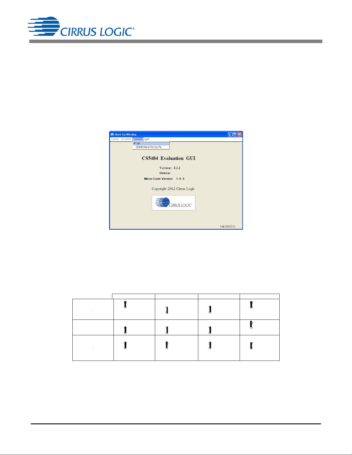
2.3 Start-up Window ............................................................................................................................... 17
2.4 Connect Menu .................................................................................................................................. 17
2.5 System Menu ................................................................................................................................... 21
2.6 Calibration Window .......................................................................................................................... 25
2.7 Conversion Window ......................................................................................................................... 27
2.8 Cirrus Test Window .......................................................................................................................... 29
Appendix A. Bill of Materials...................................................................................................................... 38
Appendix B. Schematics............................................................................................................................. 40
Appendix C. Layer Plots ............................................................................................................................. 43
DS919DB5 3
Page 4

CDB5484U
LIST OF FIGURES
Figure 1. CDB5484U Assembly Drawing and Default Configuration ................................................................ 5
Figure 2. Voltage Channel — Low-voltage Input .............................................................................................. 6
Figure 3. Voltage Channel — High-voltage Input ............................................................................................. 7
Figure 4. Current Channel — Low-voltage Input .............................................................................................. 8
Figure 5. MCU Connection Window ................................................................................................................. 9
Figure 6. Shunt Sensor Power Meter ............................................................................................................. 12
Figure 7. Current Transformer Power Meter................................................................................................... 13
Figure 8. Rogowski Coil Power Meter ............................................................................................................14
Figure 9. Standalone Power Meter Measurements ........................................................................................ 15
Figure 10. GUI Start-up Window..................................................................................................................... 17
Figure 11. Connect to the CDB board Window............................................................................................... 18
Figure 12. Connect Menu Showing Successful USB Connection .................................................................. 18
Figure 13. USB Error Message....................................................................................................................... 18
Figure 14. Connect Menu Showing Serial Connection Options...................................................................... 19
Figure 15. UART Serial Port Selection Window, UART Selected................................................................... 19
Figure 16. SPI Serial Port Selection Window, SPI Selected........................................................................... 19
Figure 17. Unknown Chip ID Error Message .................................................................................................. 20
Figure 18. System Pull-down Options ............................................................................................................ 21
Figure 19. Setup Window ............................................................................................................................... 22
Figure 20. Calibration Window........................................................................................................................ 25
Figure 21. Conversion Window.......................................................................................................................27
Figure 22. Cirrus Test Pull-down Options....................................................................................................... 29
Figure 23. Data Collection Window ................................................................................................................ 29
Figure 24. Data Collection UART Error Message...........................................................................................30
Figure 25. Data Collection Output Window..................................................................................................... 31
Figure 26. Data Collection Configuration Window .......................................................................................... 31
Figure 27. Histogram Analysis........................................................................................................................ 34
Figure 28. FFT Analysis.................................................................................................................................. 34
Figure 29. Time Domain Analysis...................................................................................................................35
Figure 30. Data Collection to File Window...................................................................................................... 36
Figure 31. Setup and Test Window ................................................................................................................ 37
Figure 32. Bill of Materials (Page 1 of 2) ........................................................................................................ 38
Figure 33. Bill of Materials (Page 2 of 2) ........................................................................................................ 39
Figure 34. Schematic - Analog Inputs............................................................................................................. 40
Figure 35. Schematic - CS5484 and Socket................................................................................................... 41
Figure 36. Schematic - Microcontroller and USB Interface............................................................................. 42
Figure 37. Top Silkscreen............................................................................................................................... 43
Figure 38. Top Routing ................................................................................................................................... 45
Figure 39. Bottom Routing.............................................................................................................................. 46
Figure 40. Solder Paste Mask ........................................................................................................................ 47
4 DS919DB5
Page 5
CDB5484U
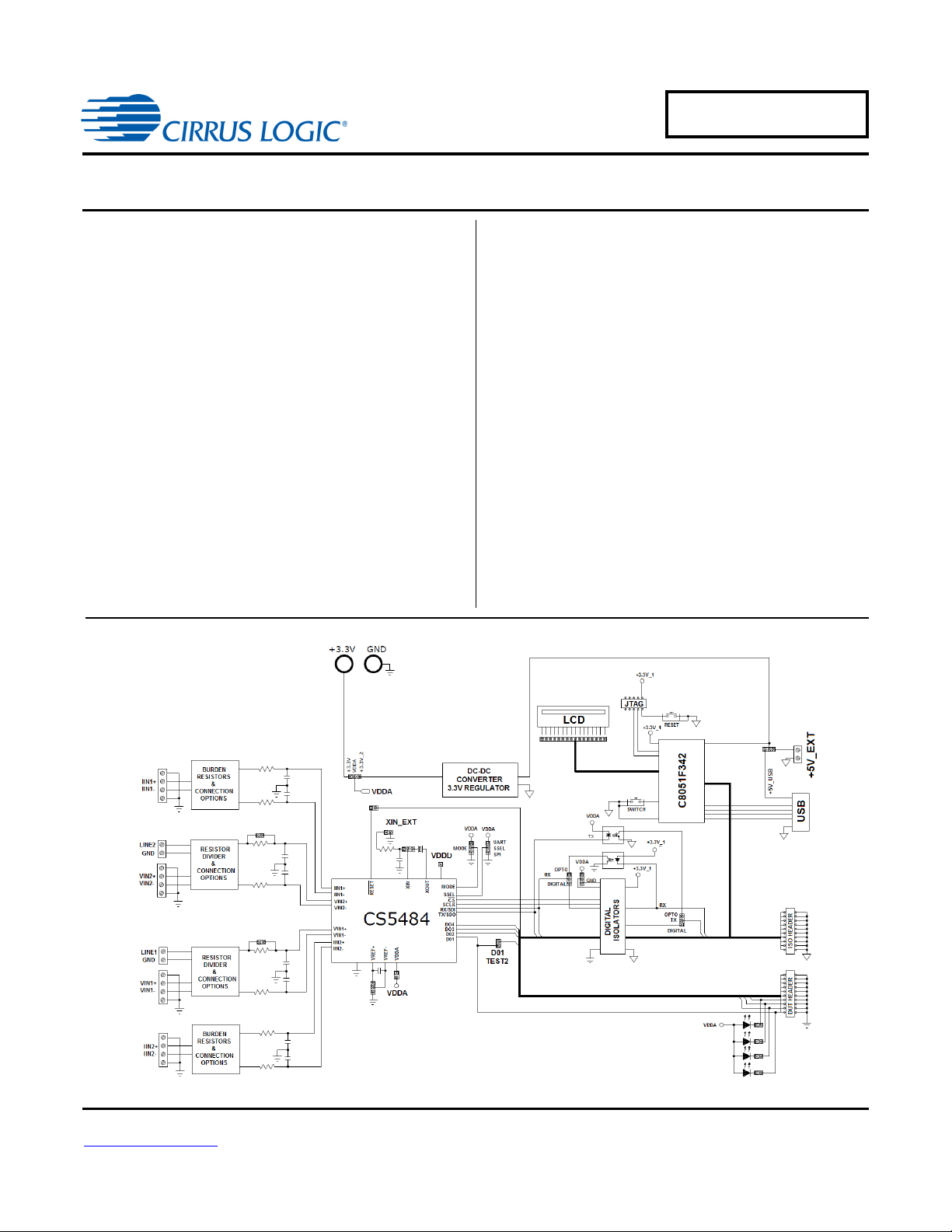
1. HARDWARE
1.1 Introduction
The CDB5484U evaluation board provides a convenient means of evaluating the CS5484 energy measurement IC. The CDB5484U evaluation board operates from a single USB or 5V power supply. An optional 3.3V power supply input is available for powering the CS5484 directly. The evaluation board
interfaces the CS5484 to a PC via a USB cable. To accomplish this, the board comes equipped with a
C8051F342 microcontroller and a USB interface. Additionally, the CDB5484U GUI software provides
easy access to the internal registers of the CS5484. The software also provides a means to display the
on-chip ADC performance in the time domain or frequency domain.
1.2 Evaluation Board Overview
The board is partitioned into two main sections: analog and digital. The analog section consists of the
CS5484, passive anti-aliasing filters, and a high-voltage section with attenuation resistor networks. The
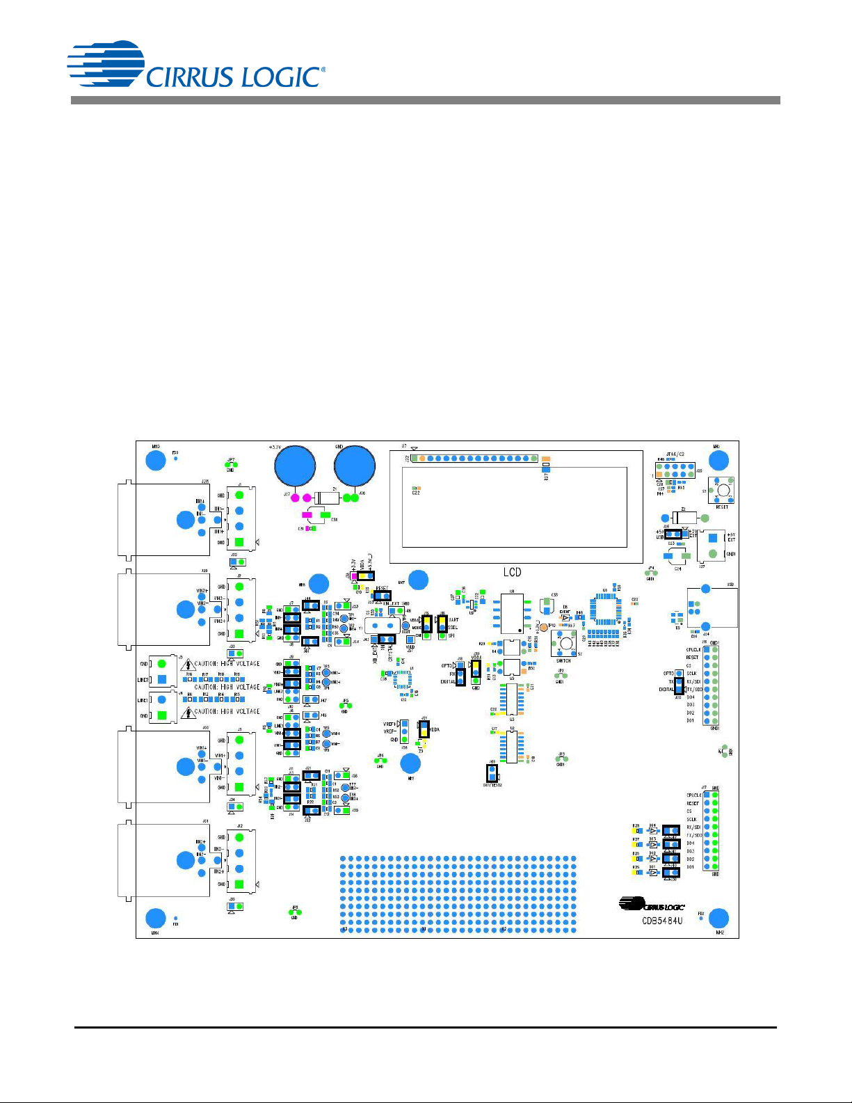
digital section consists of the C8051F342 microcontroller, LCD, test switches, reset circuitry, and USB interface. The board also has a user-friendly power supply connection. The assembly information and default configurations for jumpers are shown below.
Figure 1. CDB5484U Assembly Drawing and Default Configuration
DS919DB5 5
Page 6
CDB5484U
O VIN1-
O O VIN1-
GND
VIN1-
(Default)
O VIN1+
O O VIN1+
O O VIN1+
GND
Line1
VIN1+
(Default)
O VIN2-
O O VIN2-
VIN2-
GND
(Default)
O VIN2+
O O VIN2+
O O VIN2+
VIN2+
Line2
GND
(Default)
O VIN1-
O O VIN1-
GND
VIN1-
O VIN1+
O O VIN1+
O O VIN1+
GND
Line1
VIN1+
O VIN2-
O O VIN2-
VIN2-
GND
O VIN2+
O O VIN2+
O O VIN2+
VIN2+
Line2
GND
O VIN1-
O O VIN1-
GND
VIN1-
O VIN1+
O O VIN1+
O O VIN1+
GND
Line1
VIN1+
O VIN2-
O O VIN2-
VIN2-
GND
O VIN2+
O O VIN2+
O O VIN2+
VIN2+
Line2
GND
O VIN1-
O O VIN1-
GND
VIN1-
O VIN1+
O O VIN1+
O O VIN1+
GND
Line1
VIN1+
O VIN2-
O O VIN2-
VIN2-
GND
O VIN2+
O O VIN2+
O O VIN2+
VIN2+
Line2
GND
VIN1+/VIN2+
VIN1-/VIN2-
250 mVp
CDB5484U
CS5484
J3/J2
J6/J10
J11/J9
C4/C8
0.027UF
C9/C7
0.027UF
R6/R4
1K
R7/R3
1K
J45/J47
VIN1+/VIN2+
VIN1-/VIN2-
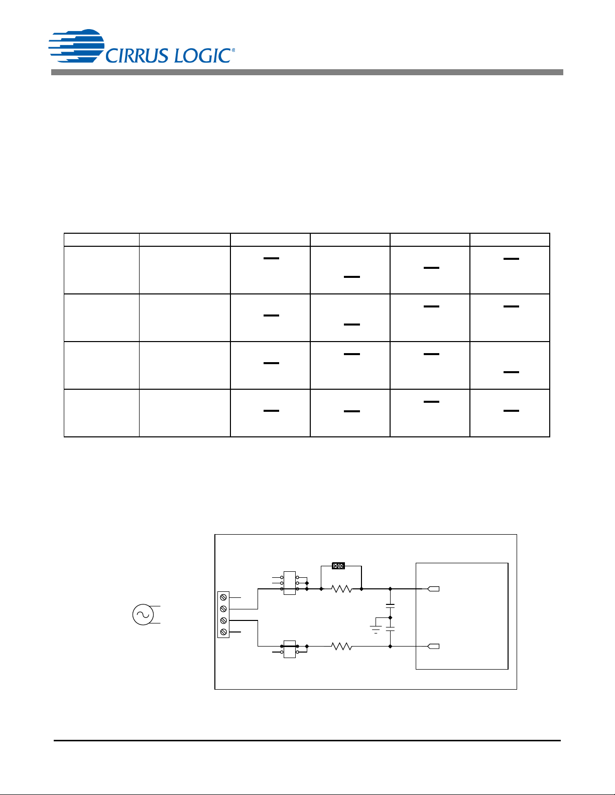
1.3 Analog Section
The analog section of the CDB5484U is highly configurable. Onboard signal conditioning options for the
voltage and current channels enable most applications to interface directly to the sensors. The following
two sections define the voltage and current channel configurations.
1.3.1 Voltage Sensor Connection
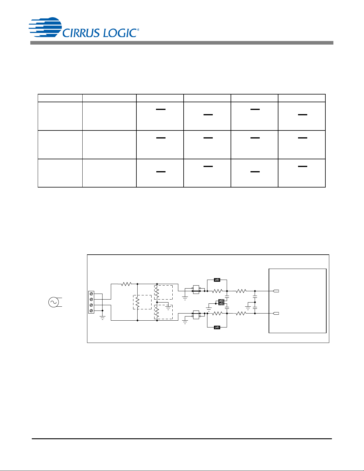
There are three input signal options for the voltage channel inputs (VIN1±, VIN2±) which include an external low-voltage signal (via screw terminals or XLR connections), high-voltage line inputs, or GND.
Table 1 illustrates the options available.
Table 1. Voltage Channel Input Signal Selection
INPUT Description J11 J6 J9 J10
Selects External
VIN1± or VIN2±
VIN1± or VIN2±
Low-voltage Fully
Differential Signal
Selects External
Low-voltage Single-ended Signal
GND
High Voltage
Line1 or Line2
Selects Grounding
the Input
Selects External
High-voltage AC
Line Signal
The CDB5484U evaluation board provides screw-type terminals (J3 and J2) or XLR connectors (J30 and
J29) to connect low-voltage input signals to the voltage channels (see Figure 2). The screw terminals are
labeled as VIN1+ / VIN1- and VIN2+ / VIN2-. An R-C network at each channel input provides a simple
configurable anti-alias filter. By installing jumpers on J6 to position VIN1+, J11 to position VIN1-, J10 to
position VIN2+, and J9 to position VIN2-, the input voltage signal is supplied from the screw terminals or
XLR connections.
6 DS919DB5
Figure 2. Voltage Channel — Low-voltage Input
Page 7
CDB5484U
GND
LINE1/LINE2
CS5484
CDB5484U
NEUTRAL
LINE
J4/J5
J11/J9
J6/J10
R5/R10
1K
C9/C7
0.027UF
C4/C8
0.027UF
R7/R3
1K
R6/R4
1K
R8/R16
422K
R12/R17
422K
R14/R18
422K
R15/R19
422K
J45/J47
VIN1-/VIN2-
VIN1+/VIN2+
1k
4422k1k+
------------------------- ---------------
1
1689
-------------
=
300Vrms
250mVp
2
-----------------------
1689=
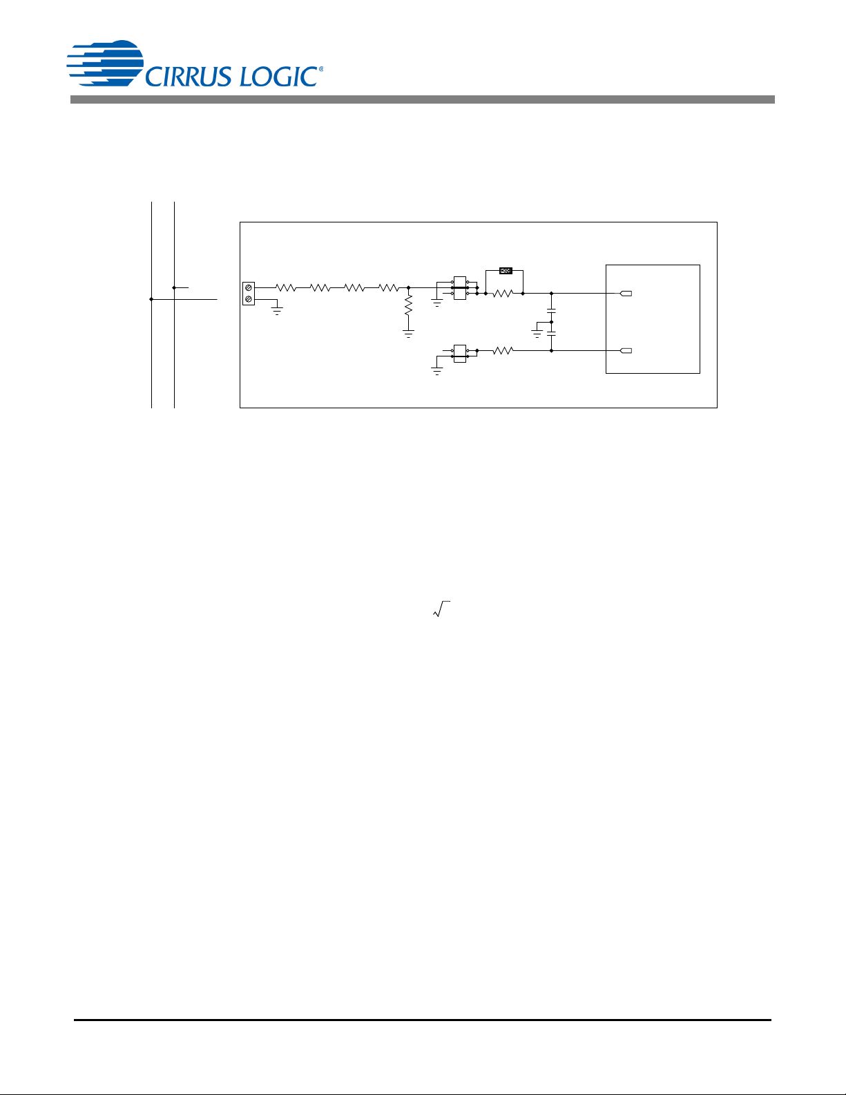
The CDB5484U evaluation board provides screw-type terminals (J4 and J5) to connect high-voltage line
inputs. By installing jumpers on J6 to position LINE1, J10 to position LINE2, J11 to position GND, and J9
to position GND, the input voltage signal is supplied from the high-voltage inputs. Extreme care should be
used when connecting high-voltage signals to the CDB5484U evaluation board (see Figure 3).
Figure 3. Voltage Channel — High-voltage Input
The default attenuation networks provide the following attenuation:
With the CS5484 input range of 250mVp at a maximum AC line input of:
is acceptable. It is recommended to apply a 10% margin for the AC line input (270Vrms).
The CDB5484U evaluation board provides input shorting options for calibration and noise performance
measurements. With a jumper on J6, J11, J10, and J9 in the GND position, the inputs are connected to
analog ground (GND).
DS919DB5 7
Page 8
CDB5484U
O IIN1+
O O IIN1+
IIN1+
GND
(Default)
O IIN1-
O O IIN1-
GND
IIN1-
(Default)
O IIN2+
O O IIN2+
IIN2+
GND
(Default)
O IIN2-
O O IIN2-
GND
IIN2-
(Default)
O IIN1+
O O IIN1+
IIN1+
GND
O IIN1-
O O IIN1-
GND
IIN1-
O IIN2+
O O IIN2+
IIN2+
GND
O IIN2-
O O IIN2-
GND
IIN2-
O IIN1+
O O IIN1+
IIN1+
GND
O IIN1-
O O IIN1-
GND
IIN1-
O IIN2+
O O IIN2+
IIN2+
GND
O IIN2-
O O IIN2-
GND
IIN2-
IIN1-/IIN2-
IIN1+/IIN2+
GND
GND
CS5484
CDB5484U
250 mV
J1/J12
J7/J13
J8/J14
C5/C11
0.033UF
C6/C12
0.033UF
R11/R22
NO POP
R1/R21
100
R2/R22
100
R9/R23
NO POP
R13/R24
NO POP
R49/R52 1K
R50/R53 1K
C34/C1
0.033UF
C35/C2
0.033UF
J44/J51
J46/J52
R51/R54
0
J53/J56
J54/J55
IIN1+/IIN2+
IIN1-/IIN2-
1.3.2 Current Sensor Connection
Current input options include an external signal (via screw terminals or XLR connectors) or GND. Table 2
illustrates the options available.
Table 2. Current Channel Input Signal Selection
INPUT Description J8 J7 J14 J13
Selects External
IIN1± or IIN2±
IIN1± or IIN2±
Low-voltage,
Fully Differential
Signal
Selects External
Low-voltage,
Single-ended
Signal
GND
Selects Grounding
the Input
The CDB5484U evaluation board provides two input signal options for current channels (IIN1±, IIN2±):
screw-type terminals (J1 and J2) or XLR connectors (J28 and J31) to connect input signals to the current
channels. The screw terminals are labeled as IIN1+ / IIN1-, and IIN2+ / IIN2-. An R-C network at each
channel input provides a simple configurable anti-alias filter.
By installing jumpers on J8 to position IIN1+, J7 to position IIN1-, J14 to position IIN2+, and J13 to position
IIN2-, the input current signal is supplied from the screw terminals or XLR connectors.
Figure 4. Current Channel — Low-voltage Input
The CDB5484U evaluation board provides input shorting options for calibration and noise performance
measurements. With a jumper on J8, J7, J14, and J13 in the GND position, the inputs are connected to
analog ground (GND).
8 DS919DB5
Page 9
CDB5484U
U
A
S
P
Low
s
U
A
(4800 B
a
RT
I
peed
RT
ud Max)
J16
Ƒ UART
ż SSEL
ż SPI
(default)
Ƒ UART
ż SSEL
ż SPI
Ƒ UART
ż SSEL
ż SPI
Ƒ
ż
ż
(
d
Ƒ
ż
ż
Ƒ
ż
ż
J18
OPTO
RX
DIGITAL
efault)
OPTO
RX
DIGITAL
OPTO
RX
DIGITAL
J
Ƒ
O
ż
T
ż
D
(def
a
Ƒ
O
ż
T
ż
D
Ƒ
O
ż
T
ż
D
20
PTO
X
IGITAL
ult)
PTO
X
IGITAL
PTO
X
IGITAL
J50
Ƒ VDD
A
ż EN2
ż GND
(default
)
Ƒ VDD
A
ż EN2
ż GND
Ƒ VDD
A
ż EN2
ż GND
1.4 Digital Section
The digital section contains the microcontroller, USB interface, LCD, optical isolation, JTAG header, reset
circuitry, and external interface headers (J17 and J19). The microcontroller interfaces the UART or SPI of
the CS5484 with the USB connection to the PC, enabling the GUI software to access all of the CS5484
registers and functions.
1.4.1 Serial Port Selection
Communication to the CS5484 is provided through two serial port options: UART or SPI. It is necessary
to establish communication with the MCU before establishing a serial port communication protocol with
the CS5484 (see Figure 5).
Figure 5. MCU Connection Window
For UART communication, place the SSEL jumper to the UART position via J16, and select UART in the
serial port selection window. To enable SPI communications, place the SSEL jumper to the SPI position
via J16, and select SPI in the serial port selection window. Table 3 provides the serial communication options on the CDB5484U board.
Table 3. Serial Communication Options
DS919DB5 9
Page 10

CDB5484U
1.4.2 Interface to Microcontroller
Interface headers J17 and J19 are provided to allow the CDB5484U to be connected to an external energy
registration device or an external microcontroller. Interface header J17 provides direct access to the
CS5484 pins while interface header J19 provides an isolated connection. It is imperative to use the isolated connection (J19) when high-voltage signals are used. Failure to use isolation can result in damage
to components or electrical shock. Refer to “Digital Isolation” on page 10 for details on signal isolation.
Interface header J19 can be used to connect to the external microcontroller. To connect the CS5484 to
an external microcontroller, R34, R35, R36, R37, R38, R39, R40, R41, R42, and R43 must be removed
from the board.
1.4.3 Digital Isolation
Two types of isolation are provided, including a low-speed optical coupler for UART-only and high-speed
digital isolation for UART and SPI communication. Default jumper settings provide high-speed digital isolators. To enable high-speed digital isolators, place jumpers (J18 and J20) in the RX to DIGITAL position
and TX to DIGITAL position. To enable the high-speed digital isolators, it is also necessary to install jump-
er (J50) in the VDDA position. To enable low-speed optical UART communication, place jumpers (J18 and
J20) in the RX to OPTICAL position and TX to OPTICAL position.
The high-speed digital isolators operate from DC to 150Mbps. The low-speed optical couplers operate to
a maximum speed of about 4.8kHz. All the signals supplied to the isolators are available to the MCU except CPUCLK.
1.4.4 Additional Device Pin Access
The CS5484’s digital output pins (DO1, DO2, DO3, and DO4) are routed to LEDs, which provide a simple
visual check of the digital output. Jumpers J39, J40, J41, and J42 are equipped at the factory with jumpers
to enable the LEDs. The DO1 digital output pin is supplied to the digital isolation using jumper J49.
The MODE pin jumper (J15) should be installed in the VDDA to MODE position.
The CS5484 system clock can be connected to an onboard quartz crystal, or an external clock can be
supplied to the CS5484 XIN pin though jumper J48. To connect the onboard quartz crystal, install jumper
J43 in the XIN to CRYSTAL position. To connect XIN to an external clock, install jumper J43 in the XIN to
XIN_EXT position.
10 DS919DB5
Page 11

CDB5484U
Sup
p
Sou
r
US
B
Externa
l
&
US
B
Extern
a
ly
ce
C
S
S
o
O
n
3
R
e
+3.3V
B
l +5V
O
n
3
re
g
5484
urce
Bi
p
J3
-board
.3 V
gulator
inding
Post
+
-board
.3V
ulator
nding
ost
6&J37
U
S
u
J
NC
+
3.3 V
+
NC
N
SB
pply
24
5
Ter
m
J
5V
N
5V
N
C
+
V
inals
27
J
C
Ƒ
V
ż
V
(d
e
C
Ƒ
V
ż
V
5V
Ƒ
V
ż
V
VDDA
J21
DDA
DDA
fault)
Ƒ
+
ż
V
ż
+
(d
DDA
DDA
Ƒ
+
ż
V
ż
+
DDA
DDA
Ƒ
+
ż
V
ż
+
J38
+
3.3V
DDA
3.3V_2
efault)
Ƒ
ż
ż
(
3.3V
DDA
3.3V_2
Ƒ
ż
ż
3.3V
DDA
3.3V_2
Ƒ
ż
ż
3.3V_1
J26
+5V EXT
+5V
+5V USB
default)
+5V EXT
+5V
+5V USB
+5V EXT
+5V
+5V USB
1.5 Power Supply Section
Table 4 illustrates the power supply connections on the evaluation board. The positive analog (VDDA) for
the CS5484 can be supplied using the +3.3V binding post (J36 and J37) or the onboard +3.3V regulator.
Jumper J38 allows the VDDA supply to be sourced from the +3.3V binding post (J37) or the regulated
+3.3V supply. The DC-DC converter (U8) powers the onboard +3.3V regulator. Jumper J26 allows the
+5V supply to be sourced from either the +5V EXT screw connector (J27) or the +5V USB supply. The
+5V supplies the power for the microcontroller (8051_REGIN) and the DC-DC converter (U8). Jumper J21
is used to measure the CS5484 analog supply current and must be installed.
When connecting the CDB5484U board to the AC line through non-isolated sensors, it is strongly recommended that the CS5484 GND reference is connected to the neutral, the non-isolated current sensor is
connected to the neutral, and the CS5484 is supplied by +3.3V isolated from AC line. The DC-DC converter (U8) provides 1kVDC isolation, while no isolation is provided for the 3.3V binding post connections.
If +3.3V is used from the binding post, then the external 3.3VDC power supply must be isolated from the
AC line. To prevent electric shock and damages, always use an isolated power source.
Table 4. Power Supply Selection
DS919DB5 11
Page 12
CDB5484U
IIN1-/IIN2-
IIN1+/IIN2+
GND
GND
GND
LINE1/LINE2
CS5484
CDB5484U
PHASE
NEUTRAL
J1/J12
J4/J5
J7/J13
J8/J14
J11/J9
J6/J10
R5/R10
1K
C5/C11
0.033UF
C6/C12
0.033UF
C9/C7
0.027UF
C4/C8
0.027UF
R11/R22
NO POP
R1/R21
100
R2/R22
100
R7/R3
1K
R6/R4
1K
R9/R23
NO POP
R13/R24
NO POP
R8/R16
422K
R12/R17
422K
R14/R18
422K
R15/R19
422K
R49/R52 1K
R50/R53 1K
C34/C1
0.033UF
C35/C2
0.033UF
J44/J51
J46/J52
R51/R54
0
J45/J47
J53/J56
J54/J55
SHUNT
IIN1+/IIN2+
IIN1-/IIN2-
VIN1-/VIN2-
VIN1+/VIN2+
1.6 Typical Sensor Connections
The CDB5484U evaluation board provides connections directly to different types of sensors. Flexible onboard filter networks provide a convenient configuration for three common transducers: current shunt, current transformer (CT), or Rogowski coil.
1.6.1 Shunt Power Meter Example
An inexpensive current shunt configuration is easily achievable with the CDB5484U evaluation board.
Figure 6 depicts the voltage and current connections for a shunt sensor and its associated filter configurations.
It is strongly recommended that a low-side (neutral path) current shunt is used, especially in high-voltage
situations. Make sure that all signals are well connected before the power source is turned on. Extreme
care should be taken when connecting high-voltage signals to the CDB5484U evaluation board.
In this configuration it is unnecessary to use a burden resistor. A single anti-alias filter is all that is required
for the current channel. Below the filter corner frequency, the CS5484 inputs will see the same voltage
that is across the shunt. Therefore the shunt voltage should be kept below the maximum of 50mVp with
I-Channel PGA = 50x. A 10% margin is recommended for the shunt voltage (45mVp).
Figure 6. Shunt Sensor Power Meter
12 DS919DB5
Page 13
CDB5484U
V
burden
I
burden
R
burden
I
primary
N
------------------
R
burden
==
IIN1-/IIN2-
IIN1+/IIN2+
GND
GND
GND
LINE1/LINE2
CS5484
CDB5484U
PHASE
NEUTRAL
J1/J12
J4/J5
J7/J13
J8/J14
J11/J9
J6/J10
R5/R10
1K
C5/C11
0.033UF
C6/C12
0.033UF
C9/C7
0.027UF
C4/C8
0.027UF
R11/R22
2.2
R1/R21
100
R2/R22
100
R7/R3
1K
R6/R4
1K
R9/R23
1K
R13/R24
1K
R8/R16
422K
R12/R17
422K
R14/R18
422K
R15/R19
422K
R49/R52 1K
R50/R53 1K
C34/C1
0.033UF
C35/C2
0.033UF
J44/J51
J46/J52
R51/R54
0
J45/J47
J53/J56
J54/J55
IIN1+/IIN2+
IIN1-/IIN2-
VIN1-/VIN2-
VIN1+/VIN2+
1.6.2 Current Transformer Power Meter Example
A slightly more expensive option is to use a current transformer (CT) to connect the AC current to the
CDB5484U evaluation board. Figure 7 depicts the voltage and current connections for a CT sensor and
its associated filter configurations.
NEVER “open circuit” a CT. Make sure that all signals are well connected before the power source is
turned on. Extreme care should be taken when connecting high-voltage signals to the CDB5484U evaluation board.
The burden resistor (R11/R22) is necessary in a CT application to convert the secondary current into voltage. Knowledge of the current transformers turns ratio (N) is key to determining the proper CS5484 input
voltage (V
maximum current input should be 10% less than the maximum channel voltage of 250mVp with I-channel
PGA = 10x. The secondary voltage (V
ondary current. Then the secondary current (I
) that the meter places on the system. The optimum secondary voltage (V
burden
) is determined by converting the primary current to the sec-
burden
) can be converted into a voltage by Ohm's Law.
burden
burden
) at the
The secondary voltage (V
) is sourced to the CS5484 through a simple low-pass, anti-alias filter, and
burden
this voltage should not exceed the 250mVp.
Figure 7. Current Transformer Power Meter
DS919DB5 13
Page 14
CDB5484U
IIN1-/IIN2-
IIN1+/IIN2+
GND
GND
GND
LINE1/LINE2
CS5484
CDB5484U
PHASE
NEUTRAL
J1/J12
J4/J5
J7/J13
J8/J14
J11/J9
J6/J10
R5/R10
1K
C5/C11
0.033UF
C6/C12
0.033UF
C9/C7
0.027UF
C4/C8
0.027UF
R11/R22
NO POP
R1/R21
100
R2/R22
100
R7/R3
1K
R6/R4
1K
R9/R23
NO POP
R13/R24
NO POP
R8/R16
422K
R12/R17
422K
R14/R18
422K
R15/R19
422K
R49/R52 1K
R50/R53 1K
C34/C1
0.033UF
C35/C2
0.033UF
J44/J51
J46/J52
R51/R54
0
J45/J47
J53/J56
J54/J55
IIN1+/IIN2+
IIN1-/IIN2-
VIN1-/VIN2-
VIN1+/VIN2+
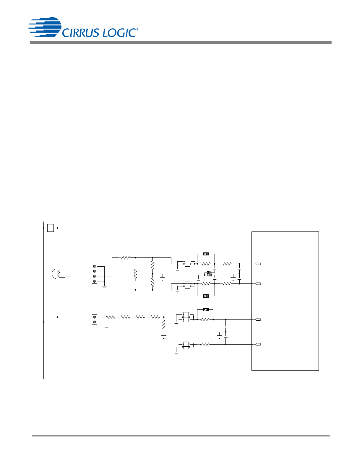
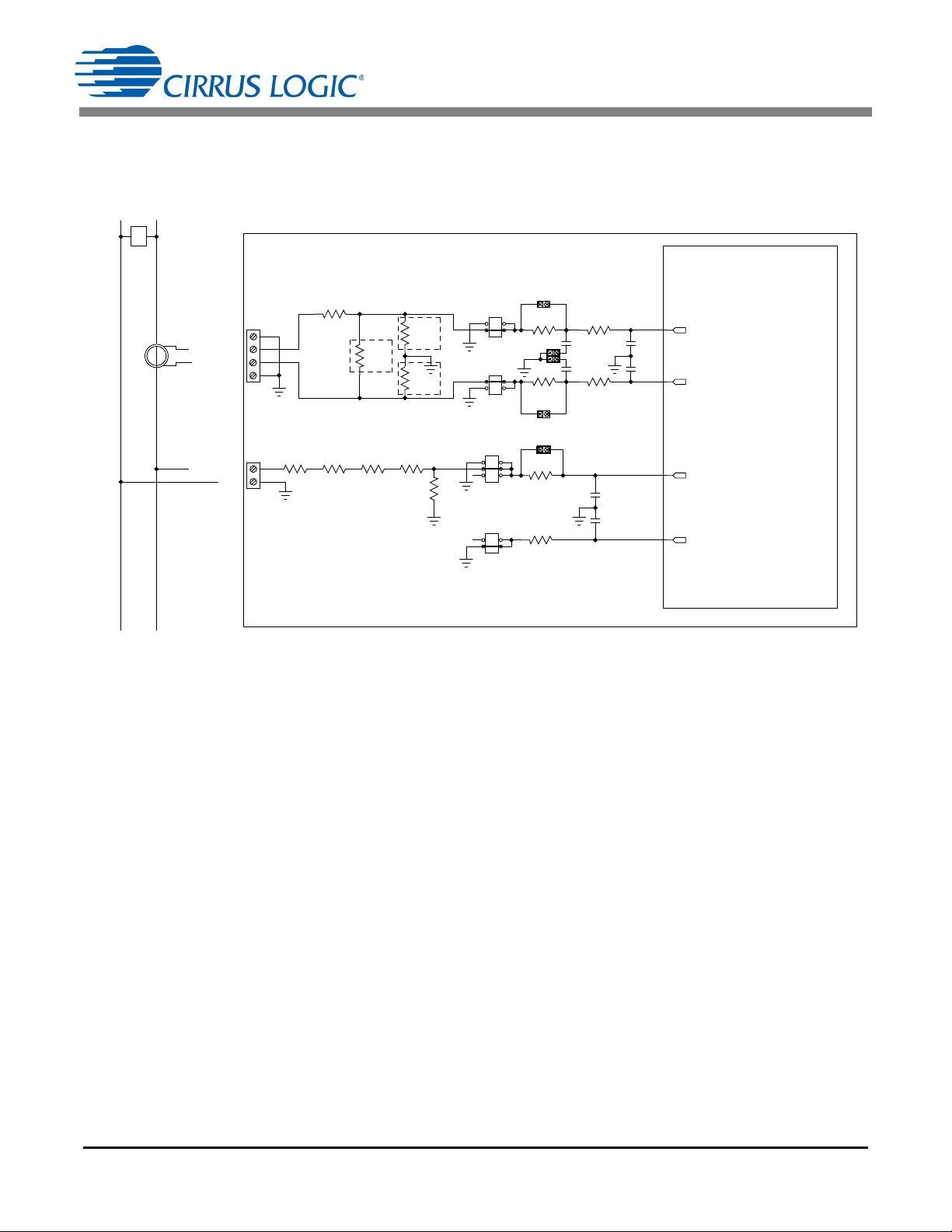
1.6.3 Rogowski Coil Power Meter Example
Rogowski coil power meter can be connected to the CDB5484U evaluation board. Figure 8 shows the
voltage and current connections for the Rogowski sensor and its associated filter configurations.
Figure 8. Rogowski Coil Power Meter
For more information, see AN365: Using the CS5480/84/90 Energy Measurement IC with Rogowski Coil
Current Sensors.
14 DS919DB5
Page 15
CDB5484U
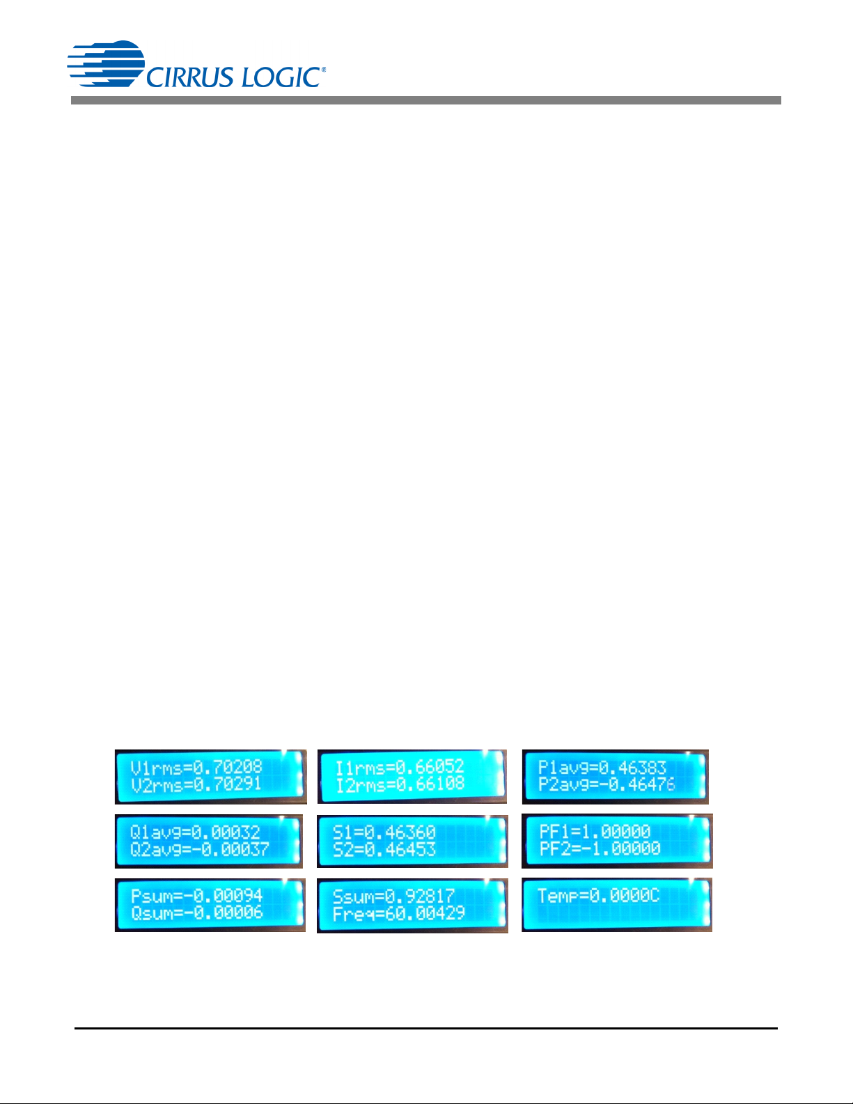
1.7 Standalone Meter Application
The CDB5484U evaluation board provides a standalone power meter using the CS5484, MCU, and LCD.
The user can enable the power meter by connecting the sensors to the analog inputs, providing power to
the board, and resetting the MCU by pressing the RESET switch. Refer to “Typical Sensor Connections”
on page 12 for details on the sensor connections and “Power Supply Section” on page 11 for details on
supply options.
The user should not use the GUI to connect the CDB5484U board. Once the GUI is connected to the
CDB5484U board the standalone power meter function is disabled and the LCD on the CDB5484U will
read "Cirrus Logic CS5484 Eval GUI". To re-enable the standalone power meter feature, close the GUI
software. The standalone power meter feature will initially show the voltage channels’ RMS register values:
V1rms = N.NNNNN and V2rms = N.NNNNN.
By clicking the onboard switch S2, the standalone power meter will display the following measurement
results:
1. RMS Voltage
2. RMS Current
3. Average Active Power
4. Average Reactive Power
5. Average Apparent Power
6. Power Factors
7. Total Active Power
8. Total Reactive Power
9. Total Apparent Power
10. Fundamental Frequency
11. CS5484 Die Temperature
Figure 9. Standalone Power Meter Measurements
DS919DB5 15
Page 16

2. SOFTWARE
CDB5484U
The evaluation board comes with software and a USB cable to link the evaluation board to the PC. The
evaluation software was developed with LabWindows
tional Instruments. The evaluation software is designed to run with Windows XP™ and Windows 7™. The
following procedure is based on Windows XP.
®
/CVI®, a software development package from Na-
2.1 Installation Procedure
Follow the steps below to install the GUI:
1. Access the following web site: http://www.cirrus.com/en/support
2. Navigate to the CDB5484U software link under Energy Measurement. The Software License web
page is displayed.
3. To agree with the terms and conditions, click the Agree button. The File Download window is displayed.
4. Click the Save button. The Save As window is displayed.
5. Select a location to store the compressed folder.
6. Click the Save button. The Download complete window is displayed.
7. Click the Open Folder button. The location where the compressed folder is stored is displayed.
8. Right-click on the compressed folder, and click Extract All.
9. Select a location to extract the files.
.
10. Navigate to the location where the extracted files are stored and double-click on the setup.exe file.
11. Click the Install button, and follow the installation instructions.
12. Execute the GUI using Section 2.1.1 Executing the GUI.
2.1.1 Executing the GUI
1. From the Start menu, click All Programs.
2. Click Cirrus Energy Measurement Evaluation (CDB5484U).
3. Click CDB5484U. The GUI is launched.
2.2 Using the Software
Before launching the software, check all jumper settings on the CDB5484U evaluation board, as described in “Evaluation Board Overview” on page 5, and connect the board to an open USB port on the PC
using the provided cable. Once the board is powered on, the software program can be launched.
16 DS919DB5
Page 17

CDB5484U
2.3 Start-up Window
When the software is launched, the Start-Up Window is displayed. This window contains information
about the software, including its title, revision number, and copyright date. The Start-Up Window is displayed in Figure 10.
Figure 10. GUI Start-up Window
A menu bar at the top displays four items: System, Cirrus Test, Connect, and Quit. Initially System and
Cirrus Test are disabled. After establishing a link to a data source, the System and Cirrus Test items will
become available.
2.4 Connect Menu
The Connect menu allows the user to establish a USB communication link with the CDB5484U board.
After the USB communication has been established, the CS5484 serial port configuration needs to be
entered according to the position of jumper J16. Connecting to the CDB5484 is a two-step process:
1. Use the “USB Item” to connect to the MCU.
2. Use the “CS5484 Serial Port Config Item” to connect the MCU to the CS5484.
2.4.1 USB Item
In the Connect menu, the USB item allows the user to establish USB communication. If the USB item in
the Connect menu is selected, the evaluation software will poll the C8051F342 microcontroller, verifying
the serial communication link is ready. When the Connect to the CDB board window is displayed (see
Figure 11), the user should reset the CDB5484 using switch (S1) on the board, wait for Windows to rec-
DS919DB5 17
Page 18

CDB5484U
Figure 11. Connect to the CDB board Window
ognize the MCU (typically 3 seconds), and then select "OK."
At this point, the USB menu item is checked, indicating that the PC has successfully communicated with
the CDB5484U evaluation board. The micro-code version information are read from the board and displayed on the screen (see Figure 12). Due to improvements to the software or new features being added,
the version displayed may be different than the image shown here.
Figure 12. Connect Menu Showing Successful USB Connection
If the evaluation software is unable to establish a communication link with the CDB5484U board, a message is displayed, indicating that the initial communication has failed (see Figure 13).
Figure 13. USB Error Message
Check to verify that the USB cable is connected properly and the power supply is on and connected properly to the CDB5484U. Reset the board (press the RESET button on the board) and try to set up the USB
connection again.
18 DS919DB5
Page 19

CDB5484U
2.4.2 CS5484 Serial Port Config Item
In the Connect menu, the CS5484 Serial Port Config item allows the user to select different types of serial
communication — UART or SPI (see Figure 14).
Figure 14. Connect Menu Showing Serial Connection Options
Before the software is configured, it is necessary to set jumper J16 on the CDB5464U board to either the
UART or SPI communication. To select UART communication, install jumper J16 in the SSEL to UART
position. To select SPI communication install jumper J16 in the SSEL to SPI position.
To select UART communications, position jumper J16 to the SSEL to UART position, and select UART in
the Serial Port Selection window (see Figure 15).
Figure 15. UART Serial Port Selection Window, UART Selected
To select SPI communications, position jumper J16 to the SSEL to SPI position, and select SPI in the Serial Port Selection window (see Figure 16).
Figure 16. SPI Serial Port Selection Window, SPI Selected
DS919DB5 19
Page 20

CDB5484U
After the serial port has been selected, press the OK button. The MCU will try to read the chip ID from the
CS5484. The chip revision number will be displayed in the Device field in the Start-Up Window. If the De-
vice field is populated with "Unknown CHIP ID", the user should check the power supply and clock to the
CS5484, MODE jumper J15, SSEL jumper J16, and the isolation jumpers J18, J51, and J20, click the RE-
SET button, and go back to the USB connection process.
Figure 17. Unknown Chip ID Error Message
20 DS919DB5
Page 21

CDB5484U
2.5 System Menu
The System pull-down provides three options: Setup CS5484, Calibration, and Conversion. Each window
provides a means to evaluate the different functions and performance of the CS5484 (see Figure 18).
Figure 18. System Pull-down Options
DS919DB5 21
Page 22

CDB5484U
2.5.1 Setup Window
The evaluation software provides access to the common CS5484's internal registers through the Setup
Window (see Figure 19). The user can access the Setup Window by selecting the Setup CS5484 item
from the System menu.
Figure 19. Setup Window
The Setup Window displays all of the common CS5484 registers in hexadecimal notation and are decoded to provide easier readability. Refer to the CS5484 data sheet for information on register functionality
and definitions. The Setup Window is segmented by function. Each subsection may contain more than
one CS5484 register in order to configure a particular function. Updating the hexadecimal value of a register will change the definitions display according to the new hexadecimal value of the register(s). Likewise, updating the definitions displayed from the list boxes will update the hexadecimal value(s) of the
associated register(s).
22 DS919DB5
Page 23

CDB5484U
2.5.1.1 Refresh Screen Button
Clicking the Refresh Screen button will update the contents of the screen by reading all the register values
from the CS5484. It is recommended to click the Refresh Screen button when entering the Setup Window,
or after modifying any registers, to reflect the current status of the CS5484.
2.5.1.2 Reset DUT Button
Clicking the Reset DUT button will software-reset the CS5484. The CS5484 will perform a software-reset,
as discussed in the CS5484 data sheet. After the software-reset, the screen contents will be automatically
refreshed with the updated status of the CS5484.
2.5.1.3 Save Config and Load Config Buttons
Clicking the Save Config button will save the current setup widow's configuration to a .txt file. Clicking the
Load Config button will recall a saved configuration and store values into the CS5484.
2.5.1.4 CS5484 MCLK Frequency
The CS5484 accepts a wide range of MCLK input frequencies and can therefore run at many different
sample rates. The frequency being used on the CS5484 should be entered in this box to provide accurate
frequency calculation in the FFT window. This will also help the software decide which functions the evaluation system can perform reliably.
2.5.1.5 Configuration Registers
In the Config0, Config1, and Config2 register boxes, the contents of the CS5484's configuration registers
can be modified by typing a hexadecimal value in the HEX field, or by changing any of the values below
the HEX field to the desired settings. Although the CDB5484U software allows the user to modify any of
the bits in the configuration registers, changing certain reserved bits, such as the NO_OSC bit of Config0,
may cause the software and board to behave erratically. This applies only to the CDB5484U evaluation
system, and not to the CS5484 chip itself.
2.5.1.6 Pulse Control Register
The Pulse Control Register section is used to make changes to, and display the contents of, the CS5484's
PulseCtrl register. The PulseCtrl register contains various bits used to select the input to each energy
pulse generation block within the CS5484. Refer to the CS5484 data sheet for descriptions of the bits.
The value of the PulseCtrl register is displayed in hexadecimal format. Most of the PulseCtrl register bits
are reserved or unused. Only the usable bits are displayed in the Setup Window.
2.5.1.7 Pulse Width and Pulse Rate Registers
The Pulse Width Register section is used to make changes to and display the contents of the CS5484's
PulseWidth register. The PulseWidth register is used to define the frequency range and pulse width of the
energy pulses generated by the CS5484. The PulseWidth register should be configured before setting the
PulseRate register. The Pulse Rate Register section is used to make changes to and display the contents
of the CS5484's PulseRate register. The PulseRate register defines the full-scale frequency of the energy
pulses generated by the CS5484.
DS919DB5 23
Page 24

CDB5484U
2.5.1.8 Phase Compensation
The Phase Comp Register section is used to make changes to, and display the contents of, the CS5484's
PC (Phase Compensation Control) register. The PC register allows coarse- and fine-phase adjustment
on each channel of the CS5484 data path. Refer to the CS5484 data sheet for descriptions of the PC reg-
ister bits.
2.5.1.9 Integrator Gain, System Gain
The Integrator Gain and System Gain sections display the signal path gain in both hexadecimal and decimal format. Each register can be modified by typing a value in the corresponding Decimal or HEX field.
2.5.1.10 Sample Count, Cycle Count, Settle Time
The Sample Count Register, Cycle Count Register, and Settle Time sections provide fields to display the
values of registers associated with low-rate calculations. The SampleCount and CycleCount registers are
entered or displayed in decimal format by default. The user may select to enter or view other number formats of the register by selecting the "d" within the field. The value of the T
hexadecimal and decimal format. Each register can be modified by typing a value in the corresponding
field.
2.5.1.11 Epsilon
register is displayed in both
Settle
The Epsilon section is used to display and adjust the Epsilon register (the ratio of the AC line frequency
to the output word rate). The Epsilon register can be updated either through entering the AC line frequency in the Line Freq field or by entering the direct register value in the HEX field.
2.5.1.12 ZX
When Automatic Frequency Update is enabled, the ZX
NUM
section is used to adjust the number of zero
NUM
crossings used in the Epsilon calculation. The update rate of Epsilon is increased by reducing the zero
crossings. The register can be modified by typing the number of zero crossings.
2.5.1.13 Mask Register
The Mask Register box displays the value for the Mask register in hexadecimal and decodes them to indicate each bit's function. The Mask register can be modified by typing a value in the HEX field, or by
checking the appropriate boxes for the bits that are to be masked. The value present in the Mask register
may be changed by the GUI software during certain operations to provide correct functionality of the
CDB5484U board.
2.5.1.14 Temperature Registers
The Temperature Registers box is used to adjust the temperature offset register (T
gain register (T
) to convert the temperature register (T) from the Celsius scale to the Fahrenheit scale,
GAIN
) and temperature
OFF
or vice versa, and to improve temperature measurement accuracy. Refer to the CS5484 data sheet for
the details of the on-chip temperature sensor.
2.5.1.15 V/I Zero-crossing Level and No Load Threshold
The V/ I Zero-crossing Level and No Load Threshold boxes display the values for these registers in hexadecimal and decimal. Each register can be modified by typing a value in the corresponding Decimal or
HEX field.
24 DS919DB5
Page 25

CDB5484U
2.5.1.16 V1/V2 Sag, V1/ V2 Swell, and I1/I2 Overcurrent Registers
The registers for voltage sag, voltage swell, and overcurrent are displayed in the V1 Sag, V2 Sag, V1
Swell, V2 Swell, I1 Overcurrent, and I2 Overcurrent Register sections. These sections display the level
and duration values of the corresponding registers in both hexadecimal and decimal format. Each register
can be modified by typing a value in the corresponding decimal or HEX field. Refer to the CS5484 data
sheet for detailed descriptions of these registers.
2.5.1.17 Register Checksum, SerialCtrl Registers
The Register Checksum and SerialCtrl Register boxes provide control and status of critical serial port
communication parameters and the register checksum. The SerialCtrl Register section provides control
over RX pin, baud rate, and enabling checksum protection for serial communication. The Register Check-
sum section provides the calculated checksum of the critical registers inside the CS5484. The register
checksum updates automatically after single or continuous conversion has been performed. The RegChk
and SerialCtrl registers are displayed in hexadecimal form. Note that if the opto-couplers are selected as
the isolation (J18, J20), the maximum baud rate is 2400.
The baud rate field applies only to UART serial communication and can be changed by the pull-down field.
It is recommended to set the baud rate to the highest setting possible. The default setting of 600 baud will
cause some GUI functions to overflow the communication buffer and not function correctly.
2.6 Calibration Window
The Calibration Window is used to display and write to the CS5484 offset and gain calibration registers.
The user is also able to initiate the CS5484's calibration sequences that are used to set the calibration
values. AC offset, DC offset, and gain calibrations can be performed on the voltage channel, the current
channel, or both simultaneously. The user should refer to the CS5484 data sheet for more details on calibration (see Figure 20).
Figure 20. Calibration Window
DS919DB5 25
Page 26

CDB5484U
The Refresh Screen button will update the contents of the screen by reading all the register values from
the part. It is recommended to click the Refresh Screen button when entering the Calibration Window, or
after modifying any registers to reflect the current status of the CS5484.
2.6.1 Save Cal and Load Cal Buttons
Clicking the Save Cal button will save the calibration widow's configuration to a .txt file. Clicking the Load
Cal button will recall a saved configuration and store values into the CS5484.
2.6.2 Offset/Gain Register
In the Offset and Gain Calibration boxes, the offset and gain registers for all channels are displayed in
hexadecimal and decimal formats. These registers can be modified directly by typing the desired value in
the display boxes. There are three types of offset registers: DC offset, AC offset, and power offset. The
AC offset registers only affect the RMS register values. The active and reactive power offset registers only
affect the active and reactive power register values, respectively. The DC, AC, and power offset registers
are two's complement numbers whose values range from -1 to +1. The gain register value ranges from 0
to 4.
2.6.3 Performing Calibrations
AC/DC offset and gain calibrations can be performed on both the voltage and current channels of the
CS5484. It is recommended to software-reset the CS5484 before running calibrations because the initial
values in the calibration registers will affect the results of the calibration. A software-reset will reset these
registers back to the default values of zero offset and unity gain. AC/DC offset calibration should be performed before gain calibration to ensure accurate results.
2.6.3.1 Offset Calibrations
1. Ground the channel(s) that need to be calibrated directly at the channel header(s), J6, J10, J11, and
J9 for the voltage channels and J7, J8, J13, and J14 for the current channels. The channel(s) could
also be grounded directly at the screw-type terminals.
2. Press the corresponding AC or DC offset calibrate button (Cal V, Cal I, or Calibrate All Channels) in
the corresponding Offset Calibration box(es).
3. The offset register value(s) will automatically update when the calibration is completed.
2.6.3.2 Gain Calibrations
1. Attach an AC or DC calibration signal to the screw-type terminals, and make sure the corresponding
channel headers (J6, J7, J8, J9, J10, J11, J13, and J14) are set to the desired input position.
2. Press the corresponding gain calibrate button (Cal V, Cal I, or Calibrate All Channels) in the corre-
sponding Gain Calibration box(es).
3. The gain register value(s) will automatically update when the calibration is completed.
The Calibration window also contains the Active and Reactive Power Offset Register 1 and Register 2
display and adjustment. The user can read and write the values in the CS5484 active and reactive power
offset registers (P1
OFF
, P2
OFF
, Q1
OFF
, and Q2
OFF
).
26 DS919DB5
Page 27

CDB5484U
2.7 Conversion Window
The Conversion Window allows the user to see the results of single and continuous conversions and the
CS5484 status, perform data averaging, and use the power-saving modes of the CS5484. The Conversion Window can be accessed from the System pull-down menu, Conversion menu item. The Conversion
Window provides the active, apparent, and reactive energy calculation register results for each channel.
In addition, the RMS, power factor, and peak signal amplitudes for each analog-to-digital converter channel, chip temperature (when temperature measurement function is enabled), AC line frequency (converted from the Epsilon register), and the values of each status register (Status0, 1, 2) are also displayed. The
Conversion Window also provides the total active, apparent, and reactive power register results.
Figure 21. Conversion Window
2.7.1 Single Conversion Button
Clicking the Single Conversion button will cause a single conversion to be performed. After a single conversion is complete, the Result column will be updated with the values present in each data register.
2.7.2 Continuous Conversion Button
Clicking this button will cause continuous conversions to be performed until the user clicks the Stop button. After each conversion is complete, the Result column will be updated with the values present in each
data register. The Mean and STD. DEV columns will be updated every N cycle, where N is the number in
the Samples to Average field. The user should stop continuous conversion before navigating away from
DS919DB5 27
Page 28

CDB5484U
this window. The Continuous Conversion button should not be used with BAUD rates less than 1200Hz
in UART mode. Using lower BAUD rates (including the default 600 baud) will result in overflowing the
communication buffer and cause other window errors, communication failure, or both.
Data logging can be enabled using the DATALOG On/Off check box and Filename field.
2.7.3 Standby Mode Button
When this button is pressed, the CS5484 will enter a standby power-saving mode. To return to normal
mode, press the Power Up button. The user should power up the device before leaving this window.
2.7.4 Power Up Button
The Power Up button is used to send the wake-up command to the CS5484. The CS5484 will return to
normal operating mode.
2.7.5 Line Frequency Result
When the AFC bit in the Config2 register is set, the Epsilon register will be calculated automatically by the
CS5484, and the Line Frequency fields will be updated automatically in continuous conversion mode. If
the AFC bit in the Config2 register is not set and the line frequency is other than the default value (50Hz),
the line frequency must be set manually here to make Epsilon be the ratio of line frequency to the output
word rate (OWR). This ensures the accuracy of the quadrature power (Q1, Q2) and the reactive power
(Q1
AVG
and Q2
) calculations. Refer to the CS5484 data sheet for more details.
AVG
2.7.6 Temperature Result
When the on-chip temperature sensor is enabled, the Temperature fields will display in the top right corner
of the Conversion Window.
2.7.7 Samples to Average
The Samples to Average field allows the user to average a number of measurement results.
28 DS919DB5
Page 29
CDB5484U
2.8 Cirrus Test Window
The Cirrus Test pull-down menu provides three options: Test and Debug, ADC Data Collection, and ADC
Data Collection to File. Each window provides a means to evaluate the different functions and perfor-
mance of the CS5484 (see Figure 22).
Figure 22. Cirrus Test Pull-down Options
2.8.1 Data Collection Window
The Data Collection window allows the user to collect sample sets of data from the CS5484 and analyze
them using time domain, FFT, and histogram plots. The Data Collection window can be accessed by pulling down the CirrusTest menu, and selecting the ADC Data Collection item (see Figure 23).
Figure 23. Data Collection Window
DS919DB5 29
Page 30
CDB5484U
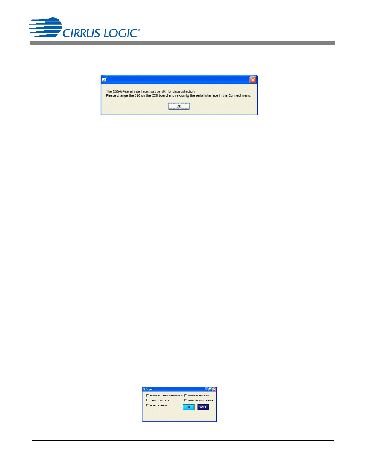
The Data Collection Window can only be accessed when operating in SPI mode. When UART serial communication is enabled, an error window will be displayed (see Figure 24). To enable SPI, refer to “Serial
Port Selection” on page 9.
Figure 24. Data Collection UART Error Message
2.8.1.1 Time Domain/FFT /Histogram Selector
The Time Domain/FFT /Histogram selector selects the type of data processing to perform on the collected
data and displays the results in the plot area. Refer to “Analyzing Data” on page 32 for more information.
2.8.1.2 Config Button
The Config button will bring up the Configuration window, which allows the user to modify the data collection specifications. Refer to “Configuration Window” on page 31 for more information.
2.8.1.3 Collect Button
The Collect button will collect data from the part to be analyzed in the plot area (see “Collecting Data Sets”
on page 32 for more information).
2.8.1.4 Output Button
The Output button will bring up a window in which the user can output the data to a file for later use, print
out a plot, or print out the entire screen. When saving data, only the data channel being displayed on the
plot will be saved to a file.
2.8.1.5 Zoom Button
The Zoom button allows the user to zoom in on the plot by selecting two points in the plot area. Press the
Restore button to return to the normal data plot, or press the Zoom button again to zoom in further.
2.8.1.6 Channel Select Button
After data collection, the two buttons labeled as “No Data" will be replaced with Current and Voltage but-
tons, allowing the user to choose the appropriate channel for display. In the time domain mode, an additional Overlay button will be present, which allows the user to display all the channels on the same plot.
2.8.1.7 Output Button and Window
The Output button allows the user to:
1. Output Time Domain File
2. Output FFT File
3. Output Histogram
4. Print Screen
5. Print Graph
Figure 25. Data Collection Output Window
30 DS919DB5
Page 31
CDB5484U
2.8.1.8 Configuration Window
The Configuration window allows the user to set up the data collection and analysis parameters (see
Figure 26).
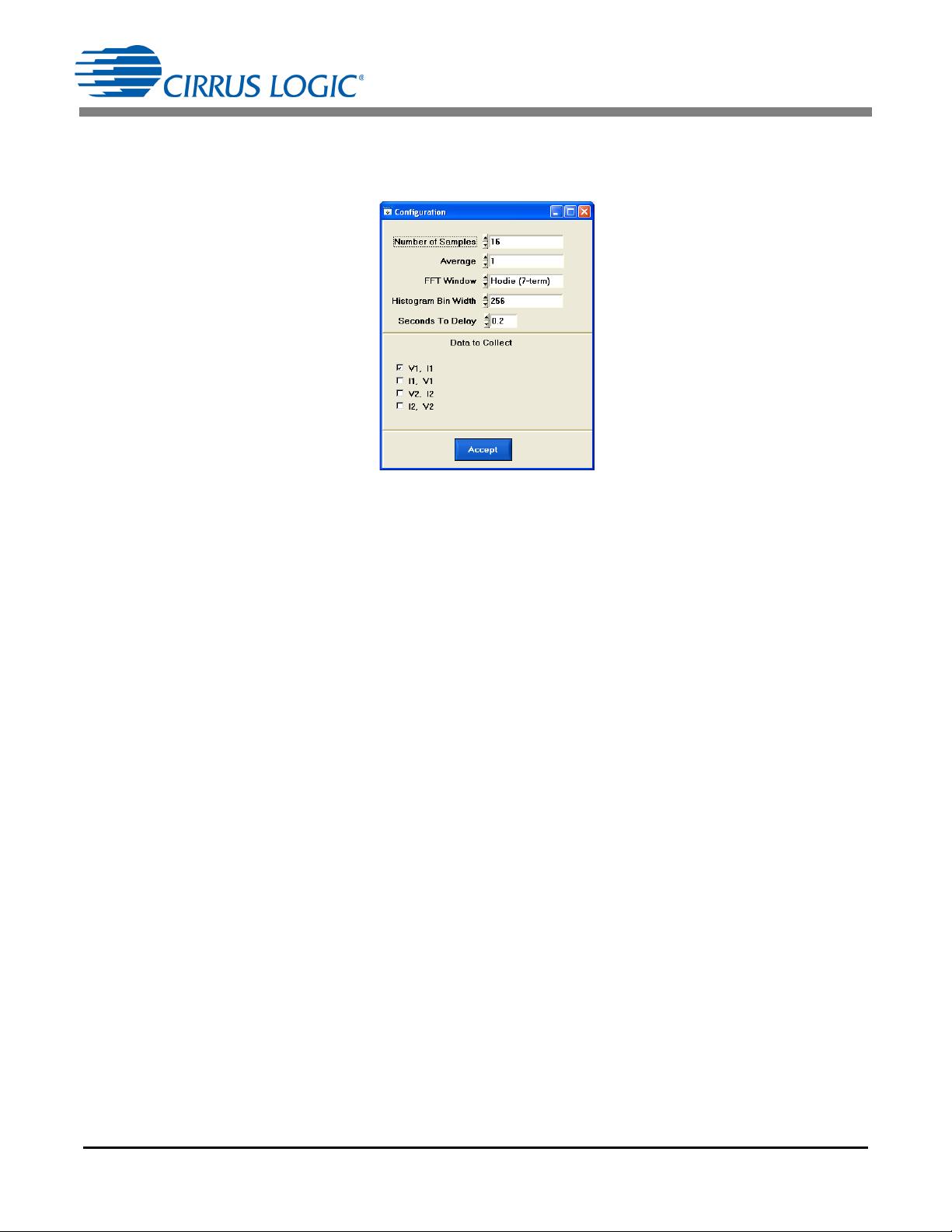
Figure 26. Data Collection Configuration Window
2.8.1.8.1 Number of Samples
The Number of Samples field allows the user to select the number of samples to collect, between 16 and
524,288.
2.8.1.8.2 Average
When performing FFT analyses, the Average field determines the number of FFTs to average. FFTs will
be collected and averaged when the Collect button is clicked.
2.8.1.8.3 FFT Window
The FFT Window box allows the user to select the type of windowing algorithm for FFT processing. Windowing algorithms include the Blackman, Blackman-Harris, Hanning, 5-term Hodie, and 7-term Hodie.
The 5-term Hodie and 7-term Hodie are windowing algorithms developed at Crystal Semiconductor, now
called Cirrus Logic.
2.8.1.8.4 Histogram Bin Width
This field determines the "bin width" when plotting histograms of the collected data. Each vertical bar in
the histogram plot will contain the number of output codes entered in this field. Increasing this number
may allow the user to view histograms with larger input ranges.
2.8.1.8.5 Seconds to Delay
This field specifies the amount of time the system waits to begin data collection after the CS5484 starts
continuous conversions.
2.8.1.8.6 Data to Collect
The Data to Collect check boxes allow the user to select the data types that will be collected and returned
to the PC for processing.
2.8.1.8.7 Accept Button
When the Accept button is clicked, the current settings will be saved, and the user will return to the Data
Collection window.
DS919DB5 31
Page 32

CDB5484U
2.8.1.9 Collecting Data Sets
To collect a sample data set:
1. In the Data Collection window, click the Config button to bring up the Configuration window and view
the current settings.
2. Select the appropriate settings from the available options (see “Configuration Window” on page 31)
and press the Accept button.
3. The Data Collection window should still be visible. Press the Collect button to begin collecting data.
4. Once the data has been collected, it can be analyzed, printed, or saved to disk.
2.8.1.10 Analyzing Data
The evaluation software provides three types of analysis tests: Time Domain, Frequency Domain, and
Histogram. The time domain analysis processes acquired conversions to produce a plot of magnitude versus conversion sample number. The frequency domain analysis processes acquired conversions to produce a plot of magnitude versus frequency using the Fast-Fourier transform (results up to Fs/2 are
calculated and plotted). Also statistical noise calculations are calculated and displayed. The histogram
analysis processes acquired conversions to produce a histogram plot. Statistical noise calculations are
also calculated and displayed.
32 DS919DB5
Page 33

CDB5484U
Mean
X
i
i0=
n1–
n
----------------------
=
STDDEV
XiMean–
i0=
n1–
n
------------------------------------------------------
2
=
Variance
XiMean–
i0=
n1–
n
------------------------------------------------------
2
=
2.8.1.11 Histogram Information
The following is a description of the indicators associated with histogram analysis. Histograms can be plotted in the Data Collection window by setting the analysis type pull-down menu to Histogram. See
Figure 27. The histogram plot information includes:
• BIN: Displays the x-axis value of the cursor on the histogram.
• MAGNITUDE: Displays the y-axis value of the cursor on the histogram.
• MEAN: Indicates the mean of the data sample set. The mean is calculated using the following
formula:
• STD_DEV: Indicates the standard deviation of the collected data set. The standard deviation is
calculated using the following formula:
• VARIANCE: Indicates the variance of the current data set. The variance is calculated using the
following formula:
• MAXIMUM: Indicates the maximum value of the collected data set.
• MINIMUM: Indicates the minimum value of the collected data set.
DS919DB5 33
Page 34

Figure 27. Histogram Analysis
Figure 28. FFT Analysis
2.8.1.12 Frequency Domain Information
CDB5484U
The following describes the indicators associated with FFT (Fast-Fourier Transform) analysis. FFT data
can be plotted in the Data Collection window by setting the analysis type selector to FFT. See Figure 28.
The FFT information includes:
• FREQUENCY: Displays the x-axis value of the cursor on the FFT display.
• MAGNITUDE: Displays the y-axis value of the cursor on the FFT display.
• S/PN: Indicates the signal-to-peak noise ratio (decibels).
• SINAD: Indicates the signal-plus-noise-plus-distortion to noise-plus-distortion ratio (decibels).
• S/D: Indicates the signal-to-distortion ratio, 4 harmonics are used in the calculations (decibels).
• SNR: Indicates the signal-to-noise ratio, first 4 harmonics are not included (decibels).
• FS-PdB: Indicates the full-scale to signal Ratio (decibels).
34 DS919DB5
Page 35

CDB5484U
2.8.1.13 Time Domain Information
The following controls and indicators are associated with time domain analysis. Time domain data can be
plotted in the Data Collection window by setting the analysis type selector to Time Domain (see
Figure 29). The time domain plot includes:
• COUNT: Displays current x-position of the cursor on the time domain display.
• MAGNITUDE: Displays current y-position of the cursor on the time domain display.
• MAXIMUM: Indicates the maximum value of the collected data set.
• MINIMUM: Indicates the minimum value of the collected data set.
Figure 29. Time Domain Analysis
DS919DB5 35
Page 36

CDB5484U
2.8.2 Data Collection to File Window
The Data Collection to File window allows the user to collect instantaneous voltage and current register
data over an extended period of time to a data file (see Figure 30). The following steps are necessary for
data collection to a file:
1. Provide the Time to Collect in seconds.
2. If a delay before data collection is needed, enter the time in seconds for the Delay.
3. Select the voltage and current channel 1 (V1,I1) or voltage and current channel 2 (V2,I2).
4. Browse to a directory and enter the file name of the desired file to save.
5. Start the data collection by pressing the START button.
6. The data collection status will be provided in Samples Collected and Time Remaining.
7. The collection will complete without any further interaction by the user, or the user may stop the data
collection at any time by pressing the STOP button.
Figure 30. Data Collection to File Window
36 DS919DB5
Page 37

CDB5484U
2.8.3 Setup and Test Window
The Setup and Test window allows the user a way to access CS5484 registers and send commands to
the CS5484 directly (see Figure 31).
Figure 31. Setup and Test Window
There are three types of transactions: Write, Read, and Send. The CS5484 memory is organized by pages. In order to properly write a register it is necessary to set the Page, Address, and Value to Write field
and then press the Write button. To read a register it is necessary to set the Page and Address and then
press the Read button. The register result will be displayed in the Value Read field. To send a command
to the CS5484, enter the command in the Command field and press the SEND button. Refer to the
CS5484 data sheet for more details on registers and commands.
DS919DB5 37
Page 38

38 DS919DB5
CIRRUS LOGIC
CDB5484U_REV_C.PL
BILL OF MATERIAL
Item Cirrus P/N Rev
Description Qty Reference Designator MFG MFG P/N Notes
Status
1 001-04187-Z1 A
CAP 0.027uF ±5% 50V X7R NPb 0805 12 C1 C 2 C4 C5 C6 C7 C8 C9 C11 C12 C34 C35 KEMET C0805C273J5RAC
A
2 001-10064-Z1 A
CAP 15pF ±5% 50V C0G NPb 0603 1 C3 KEMET C0603C150J5GAC
A
3 001-04345-Z1 A
CAP 0.1uF ±10% 50V X7R NPb 0805 2 C10 C31 KEMET C0805C104K5RAC
A
4 001-01994-Z1 A
CAP 0.01uF ±10% 16V X7R NPb 0603 2 C13 C19 MURATA GRM188R71C 103KA01D
A
5 001-02194-Z1 A
CAP 0.1uF ±10% 25V X7R NPb 0603 3 C14 C15 C16 MURATA GRM188R71E104KA01D
A
6 001-10226-Z1 A
CAP 1uF ±10% 25V X5R NPb 0603 4 C17 C18 C20 C21 MURATA GRM188R61E105KA12
A
7 001-02189-Z1 A
CAP 0.1uF ±10% 16V X7R NPb 0603 5 C22 C23 C25 C27 C29 KEMET C 0603C104K4RAC
A
8 012-00010-Z1 A
CAP 47uF ±20% 16V NPb ELEC CASE C 2 C24 C30 PANASONIC EEE1CA470WR
A
9 001-10127-Z1 A
CAP 22pF ±10% 50V C0G NPb 0603 1 C26 KEMET C0603C220K5GAC
A
10 001-04523-Z1 A
CAP 1uF ±10% 16V X7R NPb 0805 2 C28 C38 KEMET C0805C105K4RAC
A
11 001-10233-Z1 A
CAP 4.7uF ±20% 25V X7R NPb 1206 2 C32 C37 TDK C3216X7R1E475M
A
12 012-00013-Z1 A
CAP 4.7uF ±20% 25V ELEC NPb CASE B 1 C33 PANASONIC EEE1EA4R7SR
A
13 001-02194-Z1 A
CAP 0.1uF ±10% 25V X7R NPb 0603 1 C36 KEMET C0603C104K3RAC
A
14 070-00055-Z1 A
DIODE ARRAY 5V (TVS) ESD NPb SOT143 1 D5 LITTELFUSE SP0503BAHTG
A
15 165-00004-Z2 A
LED SUP RED 100mcd NPb SMD 5 D6 DO1 DO2 DO3 DO4 EVERLIGHT 28-21SRC/TR8
A
16 110-00055-Z1 A
CON TERM BLCK 4 POS 5mm NPb BLU TH 4 J1 J2 J3 J12 ON-SHORE TECHNOLOGY ED 100/4DS
A
17 110-00056-Z1 A
CON TERM BLOCK 2POS 5mm NPb BLU TH 3 J4 J5 J27 ON-SHORE TECHNOLOGY ED 100/2DS
A
18 115-00016-Z1 A
HDR 3x2 ML .1"CTR 062 S GLD NP b 2 J6 J10 SAMTEC TSW-103-07-G-D
A
19 115-00257-Z1 A
HDR 2x2 ML .1" 093BD ST GLD NPb TH 6 J7 J8 J9 J11 J13 J14 SAMTEC TSW-102-08-G-D
A
20 115-00009-Z1 A
HDR 3x1 ML .1" 062 ST GLD NPb TH 9 J15 J16 J18 J20 J26 J38 J43 J50 J58 SAMTEC TSW-103-07-G-S
A
21 115-00011-Z1 A
HDR 10x2 ML .1" 062BD ST GLD NPb TH 2 J17 J19 SAMTEC TSW-110-07-G-D
A
22 115-00014-Z1 A
HDR 2x1 ML .1" 062BD ST GLD NPb TH 18
J21 J23 J39 J40 J41 J42 J44 J45 J46 J47 J48 J49 J51
J52 J53 J54 J55 J56
SAMTEC TSW-102-07-G-S
A
23 115-00276-Z1 A
HDR 16X1 ML .1" 062 S GLD NPb TH 1 J22 SAMTEC TSW-116-07-G-S SOLDER J22 TO PCB AND LCD(U7)
A
24 110-00041-Z1 A
CON RA USB BLK NPb TH 1 J24 AMP 292304-1
A
25 115-00003-Z1 A
HDR 5x2 ML .1"CTR S GLD NP b 1 J25 SAMTEC TSW-105-07-G-D
A
26 110-00014-Z1 A
CON XLR CHASSIS 3P FML SILV NPb 0 J28 J29 J30 J31 NEUTRIK NC3FD-H NO POP
A
27 115-00014-Z1 A
HDR 2x1 ML .1" 062BD ST GLD NPb TH 0 J32 J33 J34 J35 SAMTEC TSW-102-07-G-S NO POP
A
28 110-00008-Z1 A
CON BPOST 2" SILV NYLON INS BLK NPb 1 J36 JOHNSON COMPONENTS 111-0103-001
REQUIRES WIRE, 1.5L X 0.25T X 0.25T
TYPE E 24/19 BLU SQUIRES ELEC. INC.
A
29 110-00010-Z1 A
CON BPOST 2" SILV NYLON INS RED NPb 1 J37 JOHNSON COMPONENTS 111-0102-001
REQUIRES WIRE, 1.5L X 0.25T X 0.25T
TYPE E 24/19 BLU SQUIRES ELEC. INC.
A
30 115-00024-Z1 A
HDR 1x1 ML .1"CTR S NPb GL D 1 J57 SAMTEC TSW-101-07-G-S
A
31 080-00004-Z1 A
WIRE JUMPER 2P 0.1" BRASS NPb TH 8 JP1 JP2 JP3 JP4 JP5 JP6 JP7 JP8
COMPONENTS
CORPORATION
TP-101-10
A
32 304-00022-Z1 A
SPCR STANDOFF NYL HEX 1.0/4-40 NPb 7 MH1 MH2 MH3 MH4 MH5 MH6 MH7 KEYSTONE 1902E
REQUIRES SCREW 4-40X5X16" PH
STEEL 300-00025-Z1
A
33 020-01702-Z1 A
RES 100 OHM 1/8W ±1% NPb 0805 FILM 4 R1 R2 R21 R22 DALE CRCW0805100RFKEA
A
34 020-01816-Z1 A
RES 1k OHM 1/8W ±1% NPb 0805 FILM 10 R3 R4 R5 R6 R7 R10 R49 R50 R52 R53 D ALE CRCW08051K00FKEA
A
35 020-06362-Z1 A
RES 422k OHM 1/4W ±1% NPb 1206 8 R8 R12 R14 R15 R16 R17 R18 R19 DALE CRCW1206422KFKEA
A
Figure 32. Bill of Materials (Page 1 of 2)
APPENDIX A. BILL OF MATERIALS
CDB5484U
Page 39

DS919DB5 39
CIRRUS LOGIC
CDB5484U_REV_C.PL
BILL OF MATERIAL
Item Cirrus P/N Rev
Description Qty Reference Designator MFG MFG P/N Notes
Status
36 020-01816-Z1 A
RES 1k OHM 1/8W ±1% NPb 0805 FILM 0 R9 R13 R23 R24 DALE CRCW08051K00FKEA NO POP
A
37 021-00347-Z1 A
RES 2.2 OHM 1/8W ±5% NPb 0805 FILM 0 R11 DALE CRCW08052R20JNEA NO POP
A
38 021-01445-Z1 A
RES 2.2 OHM 1/10W ±5% NPb 0603 0 R20 DALE C RCW06032R20JNEA NO POP
A
39 021-00407-Z1 A
RES 680 OHM 1/8W ±5% NPb 0805 FILM 5 R25 R26 R27 R28 R48 DALE CRCW0805680RJNEA
A
40 021-00238-Z1 A
RES 680 OHM 1/10W ±5% NPb 0603 FILM 2 R29 R32 KOA RK73B1JTTD681J
A
41 021-00259-Z1 A
RES 5.1k OHM 1/10W ±5% NPb 0603 FIL 3 R30 R31 R47 DAL E CRCW06035K10JNEA
A
42 021-00266-Z1 A
RES 10k OHM 1/10W ±5% NPb 0603 FILM 1 R33 DALE CRCW060310K0JNEA
A
43 020-00673-Z1 A
RES 0 OHM 1/10W ±5% NPb 0603 FILM 10 R34 R35 R 36 R37 R38 R39 R40 R41 R42 R43 DALE CRCW06030000Z0EA
A
44 021-00242-Z1 A
RES 1k OHM 1/10W ±5% NPb 0603 FILM 3 R44 R45 R46 DALE C RCW06031K00JNEA
A
45 020-01473-Z1 A
RES 0 OHM 1/18W ±1% NPb 0805 FILM 2 R51 R54 DALE CRCW08050000Z0EA
A
46 020-00914-Z1 A
RES 130 OHM 1/10W ±1% NPb 0603 FILM 1 R55 DALE CRCW0603130RFKEA
A
47 020-00673-Z1 A
RES 0 OHM 1/10W ±5% NPb 0603 FILM 0 R56 DALE CRCW06030000Z0EA NO POP
A
48 021-00718-Z1 A
RES 20 OHM 1/3W ±5% NPb 1210 FILM 1 R57 DALE CRCW121020R0JNEA
A
49 120-00002-Z1 A
SWT SPST 130G 0/1 5mm TACT ESD NPb 2 S1 S2 ITT INDUSTRIES PTS645TL50 LFS INSTALL AFTER WASH PROCESS
A
50 110-00045-Z1 A
CON TEST PT .1"CTR TIN PLAT NPb BLK 10 TP1 TP2 TP3 TP4 TP5 TP6 TP7 TP8 TP9 TP10 KEYSTONE 5001
A
51 065-00332-Z4 B2
IC CRUS BIDIR ENER MEAS NPb QFN28L 1 U1 CIRRUS LOG IC CS5484-INZ/B2 ECO899, ECO935
A
52 060-00568-Z1 A
IC ISOL 5CH 2.5kV 5/0 NPb SOIC16N 1 U2 SILICON LABORATORIES Si8450BB-B-IS1
A
53 060-00567-Z1 A
IC ISOL 5CH 2.5kV 4/1 NPb SOIC16N 1 U3 SILICON LABORATORIES Si8451BB-B-IS1
A
54 175-00031-Z1 A
OPT COUP TRANS 50-600% NPb DIP4 2 U4 U5 TOSHIBA TLP781(F)
A
55 062-00229-Z1 A
IC PGM USB 64kB FLAS MCU NPb LQFP32 1 U6
SILICON LABORATORIES
INC
C8051F342-GQ PROGRAM AT TEST
A
56 160-00012-Z1 A
LCD MODULE 3.3V 16x2 16x64mm NPb 1 U7 TOP WAY LMB162AFC-2
NEED HDR16X1-SSW-116-01-G-S, TSW116-07-G-S, #2 STANDOFF .500
LENGTH, SCREWS
A
57 061-00392-Z1 A
IC DIG DC/DC CO NV 5V 1W NPb SMD8 1 U8 V-INFINITY VBT1-S5-S5-SMT
A
58 060-00319-Z1 A
IC LNR VREG μPWR 150mA NPb SOT23-5 1 U9
NATIONAL
SEMICONDUCTOR
LP2985IM5-3.3/NOPB
A
59 100-00120-Z1 A
XTL 4.096MHZ HC49US 30ppm 20pF NPb 1 Y1 ECS ECS-41-20-4X INSTALL PIN SOCKETS
A
60 070-00006-Z1 A
DIODE TR 6.8V 600W NPb AXL 2 Z1 Z2 LITTELFUSE P6KE6.8
A
61 070-00200-Z1 A
DIODE TVS 3.3V 2LN ESD NPb SOT23 1 Z3 COMCHI P TECHNOLOGY CTES033V3-G ECO852
A
62 603-00478-Z1 C
ASSY DWG CDB5484U-Z-NPb REF CIRRUS LOGIC 603-00478-Z1 ECO852
63 240-00478-Z1 C
PCB CDB5484U-Z-NPb 1 CIRRUS LOGIC 240-00478-Z1 ECO852
A
64 600-00478-Z1 C2
SCHEM CDB5484U-Z NPb REF CIRRUS LOGIC 600-00478-Z1 ECO852, ECO899, ECO 935
A
65 422-00013-Z1 D
LBL SUBASSY PRODUCT ID AND REV 1 CIRRUS LOGIC 422-00013-01
A
66 080-00003-Z1 A
WIRE BPOST 1.5X.25 24/19 GA BLU NPb 2 XJ36 XJ37 SQUIRES L-1.5X.25TX.25T_TYPE_E_
A
67 135-00003-Z1 A
SKT 1P .100"L .041"DIA GLD NPb 2 XY1(2 PINS) AUGAT 8134-HC-5P2
A
68 300-00025-Z1 A
SCREW 4-40X5/16" PH MACH SS NPb 7 XMH1 XMH2 XMH3 XMH4 XMH5 XM H6 XMH7 BUILDING FASTENERS PMSSS 440 0031 PH
A
69 110-00013-Z1 D
CON SHUNT 2P .1"CTR BLK NPb 36 MOLEX 15-29-1025 INSTALL AT TEST
A
70 422-00180-Z1 A
LBL RoHS
1
IMAGE-TEK LPP0054
PLACE LABEL ON THE SECONDARY
SIDE
A
Figure 33. Bill of Materials (Page 2 of 2)
CDB5484U
Page 40

40 DS919DB5
REV C2
2/17/11
SCHEM CDB5484U-Z NPb
600-00478-Z1
Alan ZHAAlan ZHA
3
ANALOG INPUTS
1
CHK BY/DATEINC BY/DATEDESCRIPTI ONREVECO#
SIZE B
OF
SHEET
PART #
DESCRIPTI ON:
DRAWN BY :
DATE:
ENGINEER:
SHEET TITLE:
IIN1-
IIN1+
GND
GND
GND
LINE2
GND
VIN2-
VIN2+
GND
LINE1
GND
GND
VIN1+
VIN1-
GND
GND
IIN2-
IIN2+
GND
GND
IIN1+
GND
IIN1-
GND
VIN2-
GND
LINE2
VIN2+
GND
LINE1
VIN1+
VIN1-
GND
GND
IIN2+
IIN2-
GND
INITIAL DESIGN
Alan ZHA
Alan ZHA
09/09/10 09/09/10
A
ADDED U9,C32,C36,C37, C38
Alan ZHA
Alan ZHA
09/09/10 09/09/10
B
ECO812
CIRRUS DEVICE REVISION CS5484-INZ/A0 TO A1
DARREN B.
Alan ZHA
02/17/11 02/17/11
B1
ECO831
CHANGED SILK FROM CAUTIO N TO DANGER
C
ECO852
JOE GARZA
Alan ZHA
05/19/11
05/19/11
CHANGED Z3 TO CTES033V3-G AND U1 FOOTPRI NT
ECO899 C1 CHGD U1 TO CS5484-INZ/B0
A. GARZA Al an ZHA
05/19/11 05/19/11
ECO935 C2 CHGD U1 TO CS5484-IN Z/B2
A. GARZA
3/12/12
Alan Zha
3/12/12
NOT ES: UNL ESS OTHE RW SIE SPE CI FI ED:
1. ALL RE SIST OR VAL UE S ARE IN OH MS.
1
2
3
4
J1
1
2
3
4
J2
1
2
J5
1
2
34
J7
1
2
34
J8
1
2
34
J9
HDR2X2
1
2
34
56
J10
HDR3X2
R10
1K
C5
0.027UF
X7R
C6
0.027UF
X7R
C7
0.027UF
X7R
C8
0.027UF
X7R
R11
2.2
NO POP
R1
100
R2
100
R3
1K
R4
1K
R9
1K
NO POP
R13
1K
NO POP
R16
422K
R17
422K
R18
422K
R19
422K
1
2
3
4
J3
1
2
J4
1
2
34
56
J6
HDR3X2
1
2
34
J11
HDR2X2
R5
1K
C4
0.027UF
X7R
C9
0.027UF
X7R
R6
1K
R7
1K
R8
422K
R12
422K
R14
422K
R15
422K
1
2
3
4
J12
1
2
34
J13
1
2
34
J14
C11
0.027UF
X7R
C12
0.027UF
X7R
R20
2.2
NO POP
R21
100
R22
100
R23
1K
NO POP
R24
1K
NO POP
12
3
NEUTRIK
2
1
3
4
J28
XLR-FE-NEUTRIK-NC3FD-H
NO POP
12
3
NEUTRIK
2
1
3
4
J29
XLR-FE-NEUTRIK-NC3FD-H
NO POP
12
3
NEUTRIK
2
1
3
4
J30
XLR-FE-NEUTRIK-NC3FD-H
NO POP
12
3
NEUTRIK
2
1
3
4
J31
XLR-FE-NEUTRIK-NC3FD-H
NO POP
J32
NO POP
J33
NO POP
J34
NO POP
J35
NO POP
TP1
IIN1-
TP2
IIN1+
TP3
VIN2-
TP4
VIN2+
TP5
VIN1+
TP6
VIN1-
TP7
IIN2-
TP8
IIN2+
R49 1K
R50 1K
C34
0.027UF
X7R
C35
0.027UF
X7R
J44
J46
R51
0
R52
1K
R53
1K
C1
0.027UF
X7R
C2
0.027UF
X7R
J45
HDR2X1
J47
HDR2X1
J51
HDR2X1
J52
HDR2X1
J53
J54
J55
J56
R54
0
VIN2-
VIN2+
VIN1+
VIN1-
IIN1-
IIN1+
IIN2-
IIN2+
Figure 34. Schematic - Analog Inputs
REV C2
2/17/11
SCHEM CDB5484U-Z NPb
600-00478-Z1
Alan ZHAAlan ZHA
3
ANALOG INPUTS
1
CHK BY/DATEINC BY/DATEDESCRIPTI ONREVECO#
SIZE B
OF
SHEET
PART #
DESCRIPTI ON:
DRAWN BY :
DATE:
ENGINEER:
SHEET TITLE:
IIN1-
IIN1+
GND
GND
GND
LINE2
GND
VIN2-
VIN2+
GND
LINE1
GND
GND
VIN1+
VIN1-
GND
GND
IIN2-
IIN2+
GND
GND
IIN1+
GND
IIN1-
GND
VIN2-
GND
LINE2
VIN2+
GND
LINE1
VIN1+
VIN1-
GND
GND
IIN2+
IIN2-
GND
INITIAL DESIGN
Alan ZHA
Alan ZHA
09/09/10 09/09/10
A
ADDED U9,C32,C36,C37, C38
Alan ZHA
Alan ZHA
09/09/10 09/09/10
B
ECO812
CIRRUS DEVICE REVISION CS5484-INZ/A0 TO A1
DARREN B.
Alan ZHA
02/17/11 02/17/11
B1
ECO831
CHANGED SILK FROM CAUTIO N TO DANGER
C
ECO852
JOE GARZA
Alan ZHA
05/19/11
05/19/11
CHANGED Z3 TO CTES033V3-G AND U1 FOOTPRI NT
ECO899 C1 CHGD U1 TO CS5484-INZ/B0
A. GARZA Al an ZHA
05/19/11 05/19/11
ECO935 C2 CHGD U1 TO CS5484-IN Z/B2
A. GARZA
3/12/12
Alan Zha
3/12/12
NOT ES: UNL ESS OTHE RW SIE SPE CI FI ED:
1. ALL RE SIST OR VAL UE S ARE IN OH MS.
1
2
3
4
J1
1
2
3
4
J2
1
2
J5
1
2
34
J7
1
2
34
J8
1
2
34
J9
HDR2X2
1
2
34
56
J10
HDR3X2
R10
1K
C5
0.027UF
X7R
C6
0.027UF
X7R
C7
0.027UF
X7R
C8
0.027UF
X7R
R11
2.2
NO POP
R1
100
R2
100
R3
1K
R4
1K
R9
1K
NO POP
R13
1K
NO POP
R16
422K
R17
422K
R18
422K
R19
422K
1
2
3
4
J3
1
2
J4
1
2
34
56
J6
HDR3X2
1
2
34
J11
HDR2X2
R5
1K
C4
0.027UF
X7R
C9
0.027UF
X7R
R6
1K
R7
1K
R8
422K
R12
422K
R14
422K
R15
422K
1
2
3
4
J12
1
2
34
J13
1
2
34
J14
C11
0.027UF
X7R
C12
0.027UF
X7R
R20
2.2
NO POP
R21
100
R22
100
R23
1K
NO POP
R24
1K
NO POP
12
3
NEUTRIK
2
1
3
4
J28
XLR-FE-NEUTRIK-NC3FD-H
NO POP
12
3
NEUTRIK
2
1
3
4
J29
XLR-FE-NEUTRIK-NC3FD-H
NO POP
12
3
NEUTRIK
2
1
3
4
J30
XLR-FE-NEUTRIK-NC3FD-H
NO POP
12
3
NEUTRIK
2
1
3
4
J31
XLR-FE-NEUTRIK-NC3FD-H
NO POP
J32
NO POP
J33
NO POP
J34
NO POP
J35
NO POP
TP1
IIN1-
TP2
IIN1+
TP3
VIN2-
TP4
VIN2+
TP5
VIN1+
TP6
VIN1-
TP7
IIN2-
TP8
IIN2+
R49 1K
R50 1K
C34
0.027UF
X7R
C35
0.027UF
X7R
J44
J46
R51
0
R52
1K
R53
1K
C1
0.027UF
X7R
C2
0.027UF
X7R
J45
HDR2X1
J47
HDR2X1
J51
HDR2X1
J52
HDR2X1
J53
J54
J55
J56
R54
0
VIN2-
VIN2+
VIN1+
VIN1-
IIN1-
IIN1+
IIN2-
IIN2+
APPENDIX B. SCHEMATICS
CDB5484U
Page 41

REV C2
2/17/11
SCHEM CDB5484U-Z NPb
600-00478-Z1
Alan ZHAAlan ZHA
2
3
CS5484+ISOLATION
CHK BY/DATEINC BY/DATEDESCRIPTI ONREVECO#
SIZE B
OF
SHEET
PART #
DESCRIPTI ON:
DRAWN BY :
DATE:
ENGINEER:
SHEET TITLE:
DO1
DO2
DO3
DO4
TX/SDO
RX/SDI
SCLKCSRESET
CPUCLK
DO1
DO2
DO3
DO4
TX/SDO
RX/SDI
SCLK
CS
RESET
CPUCLK
DIGITA LOPTO
DIGITA L OP TO
VREF+
XIN_EXT
GND
GND
+3.3V
GND
+3.3V
+3.3V_2
VREF-
UART
SPI
GND
VDDA
VDDA
GND
CRYSTALXI N_EXT
1
XIN
2
RESET
3
IIN1-
4
IIN1+
5
VIN2-
6
VIN2+
7
VIN1+
8
VIN1-
9
IIN2-
10
IIN2+
11
VREF-
12
VREF+
13
GNDA
14
VDDA
15
DO1
16
DO2
17
DO3
18
DO4
19
TX/SDO
20
RX/SDI
21
SCLK
22
CS
23
SSEL
24
MODE
25
CPUCLK26GNDD
27
VDDD
28
XOUT
29
THERM
U1
CS5484-INZ
1
VDD1
2
A1
3
A2
4
A3
5
A4
6
A5
7
NC
8
GND19GND2
10
EN2/NC
11
B5
12
B4
13
B3
14
B2
15
B1
16
VDD2
U2
Si8450BB-B-IS1
1
VDD1
2
A1
3
A2
4
A3
5
A4
6
A5
7
EN1
8
GND1
9
GND2
10
EN2
11
B5
12
B4
13
B3
14
B2
15
B1
16
VDD2
U3
Si8451BB-B-IS1
1
A
23
E
4
C
U4
TLP781
1
A
23
E
4
C
U5
TLP781
1
2
345678
910
1112
1314
1516
1718
1920
J17
HDR10X2
12
DO1
DO1
12
DO2
DO2
12
DO3
DO3
12
DO4
DO4
R25
680
R26
680
R27
680
R28
680
Y1
J15
MODE
J16
HDR3X1
SSEL
J18
RX
R29
680
1
2
34
56
78
910
11 12
13 14
15 16
17 18
19 20
J19
HDR10X2
J20
TX
R30
5.1K
R31
5.1K
C13
0.01UF
X7R
C14
0.10uF
X7R
C15
0.10uF
X7R
C16
0.10uF
X7R
J21
VDDA
C17
1uF
C18
1uF
R32
680
C19
0.01UF
X7R
J23
R33
10K
C20
1uF
C21
1uF
J36
J37
12
Z1
P6KE6.8
6.8V
C30
47uF
ELEC
C31
0.1uF
X7R
TP9
XOUT
J38
VDDA
C32
4.7uF
X7R
C33
4.7uF
ELEC
J39
J40
J41
J42
J43
XIN
J49
DO1/TEST2
J50
ASSY D WG-
603-00478-Z1
PCB DWG-
240-00478-Z1
SCHEMA TIC DWG
600-00478-Z1
LBL SU BASSY P ROD ID A ND REV
422-00013-01
WIRE HOOK UP #6AW G STR BLU NPb
L-1.5X.25TX.25T _TYPE_E_
MH1
MH2
MH3
MH4
MH5
1
FD1
1
FD2
1
FD3
SOCKE T 1P-
8134-HC-5P2
R55
130
C3
15pF
COG
1
2
3
Z3
CTES033V3-G
J57
VDDD
J58
J48
SCREW-PHILIPS-4-40THR-P H-5/16-L-Z
PMSSS 440 0031 P H
MH6
MH7
SHUNT_2P-
15-29-1025
C10
0.1uF
X7R
1
VIN
2
GND
3
ON
5
VOUT
4
BPS
U9
C36
0.1uF
X7R
C37
4.7uF
X7R
C38
1UF
X7R
DCDC
2
+VIN
1
-VIN
4
-VO
5
+VO
U8
VBT1-S5-S5-SMT
LABEL ROHS
LPP0054
SDO
DO4
DO3
DO2
DO1
SDI
SCLK
CS
RESET
VDDA
VDDA
VDDA
VDDA
IIN1+
IIN1-
IIN2+
IIN2-
VIN1+
VIN1-
VIN2+
VIN2-
VDDA
VDDA
+3.3V_1
+3.3V_1
VDDA
+3.3V_1
+3.3V_1
VDDA
+3.3V_1
VDDA
VDDA
+3.3V_1
GND1
GND1
GND1
GND1
GND1
GND1
+5V
GND1
Figure 35. Schematic - CS5484 and Socket
DS919DB5 41
CDB5484U
Page 42
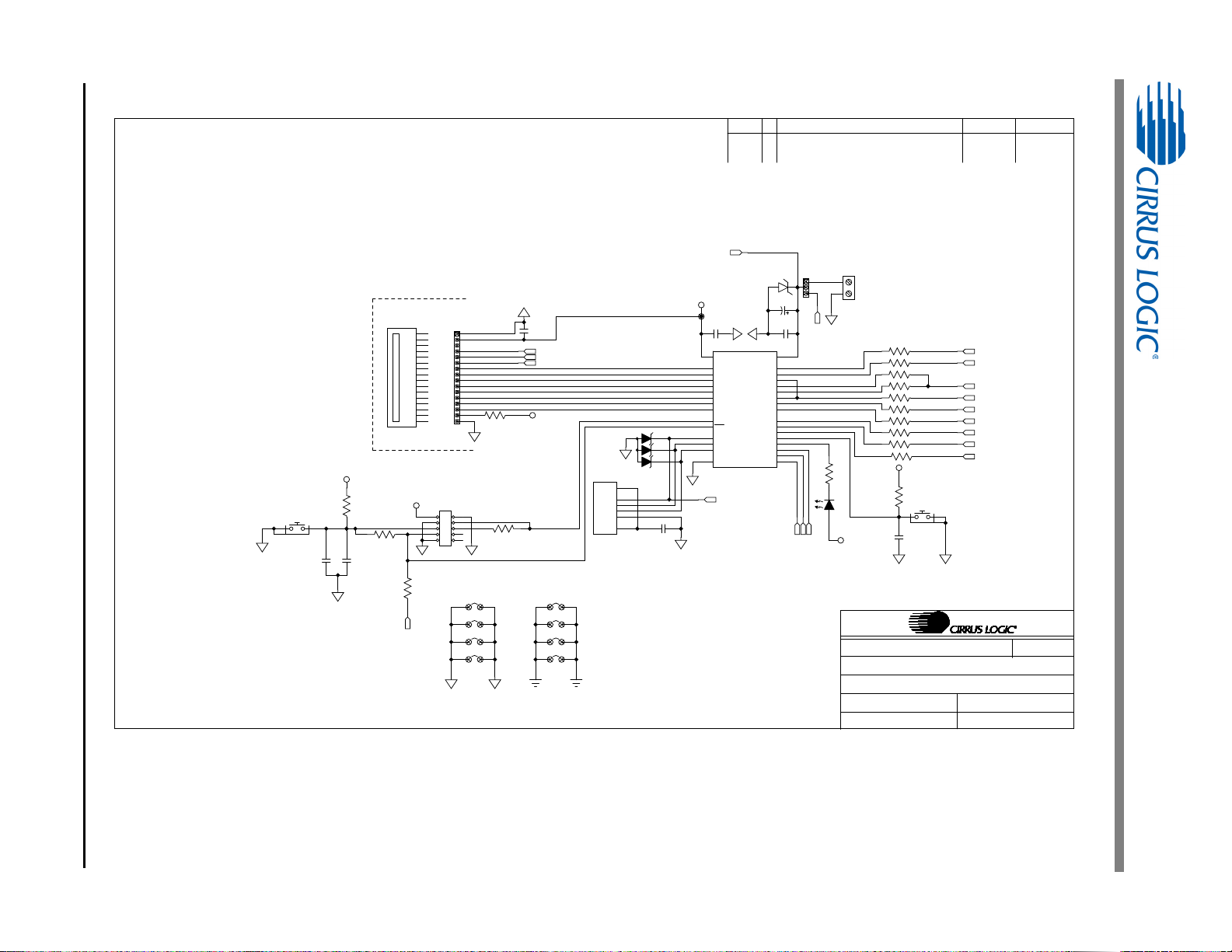
42 DS919DB5
REV C2
2/17/11
SCHEM CDB5484U-Z NPb
600-00478-Z1
3
3
Alan ZHAAlan ZHA
MCU+LCD+USB
CHK BY/DATEINC BY/DATEDESCRIPTI ONREVECO#
SIZE B
OF
SHEET
PART #
DESCRIPTI ON:
DRAWN BY :
DATE:
ENGINEER:
SHEET TITLE:
+5V_EXT
GND1
+5V_USB +5V_EXT
LCD HEADER
1
P0.1
2
P0.0
3
GND
4
D+
5
D-
6
VDD
7
REGIN
8
VBUS
9
RST/C2CK
10
P3.0/C2D
11
P2.7
12
P2.6
13
P2.5
14
P2.4
15
P2.3
16
P2.2
17
P2.1
18
P2.0
19
P1.7
20
P1.6
21
P1.5
22
P1.4
23
P1.3
24
P1.2
25
P1.1
26
P1.0
27
P0.7
28
P0.6
29
P0.5
30
P0.4
31
P0.3
32
P0.2
U6
C8051F342-GQ
1
VSS
2
VDD
3
NC
4
RS
5
R/W
6
E
7
DBO
8
DB1
9
DB2
10
DB3
11
DB4
12
DB5
13
DB6
14
DB7
15
BLA
16
BLK
U7
LCD 16P LMB162AFC-2
LCD
R34
0
R35
0
R36
0
R37
0
R38
0
R39
0
R40
0
R41
0
R42
0
C22
0.1uF
X7R
C23
0.1uF
X7R
C24
47uF
ELEC
C25
0.1uF
X7R
1
+5V
2
D-
3
D+
4
GND
5
GND
6
GND
J24
292304-1
USB
C26
22pF
431
2
D5
SP0503BAHTG
1
2
34
56
78
910
J25
HDR5X2
JTAG/C2
153
S1
RESET
R44
1K
C27
0.1uF
X7R
C28
1UF
X7R
R45 1K
R461K
J26
1
2
J27
1
5
3
S2
SWIT CH
R47
5.1K
C29
0.1uF
X7R
12
D6
RED
EVENT
R48
680
12
Z2
6.8V
TP10
+3.3V_1
JP1
JP2
JP3
JP4
JP5
JP6
JP7
JP8
R43
0
R56
0
NO POP
1
2
3
4
5
6
7
8
9
10
11
12
13
14
15
16
J22
HDR16X1-ML-TH
R57 20
SDO
SDI
CS
SCLK
DO4
DO3
DO2
DO1
LCD_E
LCD_R/W
LCD_RS
LCD_E
LCD_R/W
LCD_RS
+3.3V_1
+3.3V_1
+3.3V_1
+3.3V_1
USB_+5V
USB_+5V
+3.3V_1
+3.3V_1
GND1
GND1
GND1
GND1
GND1
GND1
GND1GND1
GND1
GND1
GND1 GND1
GND1 GND1
GND1
RESET
RESET
GND1
+5V
Figure 36. Schematic - Microcontroller and USB Interface
CDB5484U
Page 43

DS919DB5 43
Figure 37. Top Silkscreen
APPENDIX C. LAYER PLOTS
CDB5484U
Page 44

44 DS919DB5
Figure 38. Top Routing
CDB5484U
Page 45
DS919DB5 45
Figure 39. Bottom Routing
CDB5484U
Page 46
46 DS919DB5
Figure 40. Solder Paste Mask
CDB5484U
Page 47

REVISION HISTORY
Revision Date Changes
DB1 APR 2011 Initial Release.
DB2 DEC 2011 Updated screen shots and circuit diagrams to align with B0 silicon.
DB3 JAN 2012 Corrected typographical errors.
DB4 MAR 2012 Updated content.
DB5 APR 2012 Updated screen shots and circuit diagrams to align with B2 silicon.
CDB5484U
DS919DB5 47
 Loading...