

Page 1
\
CDB5466U Evaluation Board
CDB5466U
Features
Active Energy-to-Pulse Conversions
Simple Configuration Jumpers
– Current Channel Gain
– High-pass Filter
– Energy-to-pulse Output Frequency
Energy Pulses
– Collected by On-board Microcontroller
– Available on External Header
– Viewable via LEDs
Multiple Supply Voltage Selections
USB Communication with PC
On-board Voltage Reference
General Description
The CS5466 is a low cost power/energy IC with pulse
output for power measurement solutions. The
CDB5466U Evaluation Board is an inexpensive tool
designed to evaluate the functionality and performance of the CS5466.
The evaluation board is designed to output energy-topulse conversions upon power-up. The CS5466 data
sheet should be read and consulted when using the
CDB5466U evaluation board.
The evaluation board includes a microcontroller with a
USB interface. The microcontroller and GUI (Graphical User Interface) provide a means to quickly register
and evaluate the CS5466’s energy-to-pulse outputs.
ORDERING INFORMATION
CDB5466U Evaluation Board
VIN+
VIN-
IIN+
IIN-
REF+
+2.5 V
Reference
+5V
VIN+
VIN-
IIN+
IIN-
VREF SOURCE
4.096MHz
XIN
CS5466
VREFIN
VREFOUT
XOUT
IGAIN0
IGAIN1
FREQ0
FREQ1
FREQ2
E1
E2
FOUT
NEG
HPF
VD+ EXTGND
E1 E2 FOUT NEG
CONFIGURATION JUMPERS
Vu+ EXT
C8051F320
Microcontroller
USB
http://www.cirrus.com
Copyright © Cirrus Logic, Inc. 2005
(All Rights Reserved)
MAY ‘05
DS676DB1
1
Page 2

CDB5466U
TABLE OF CONTENTS
LIST OF FIGURES .................................................................................................................... 2
LIST OF TABLES ...................................................................................................................... 2
1. HARDWARE ............................................................................................................................. 3
1.1 Introduction ........................................................................................................................ 3
1.2 Evaluation Board Overview ................................................................................................ 3
1.2.1 Analog Section ...................................................................................................... 4
1.2.2 Digital Section ....................................................................................................... 5
1.2.3 Power Supply Section ........................................................................................... 8
2. SOFTWARE .............................................................................................................................. 9
2.1 Installation Procedure ........................................................................................................ 9
2.2 Using the Software ............................................................................................................. 9
2.2.1 Start-Up Window ................................................................................................... 9
2.2.2 CS5466 Pulse Rate Output Window ................................................................... 11
3. SCHEMATICS ........................................................................................................................ 13
4. LAYOUT ................................................................................................................................. 18
LIST OF FIGURES
Figure 1. CDB5466U Assembly Drawing ........................................................................................ 3
Figure 2. CDB5466U Start-up Window ........................................................................................... 9
Figure 3. Alert Window .................................................................................................................. 10
Figure 4. Quit Window................................................................................................................... 10
Figure 5. CDB5466 Evaluation Board ........................................................................................... 11
Figure 6. CDB5466U Pulse Rate Output Window......................................................................... 11
Figure 7. Analog Inputs ................................................................................................................. 13
Figure 8. CS546x and Socket ....................................................................................................... 14
Figure 9. CS5462 and CS5466 Configuration............................................................................... 15
Figure 10. Microcontroller and USB Interface ............................................................................... 16
Figure 11. Power Supply ............................................................................................................... 17
Figure 1. Silk Screen ..................................................................................................................... 17
Figure 1. Topside Layer ................................................................................................................ 18
Figure 1. Bottomside Layer ........................................................................................................... 19
LIST OF TABLES
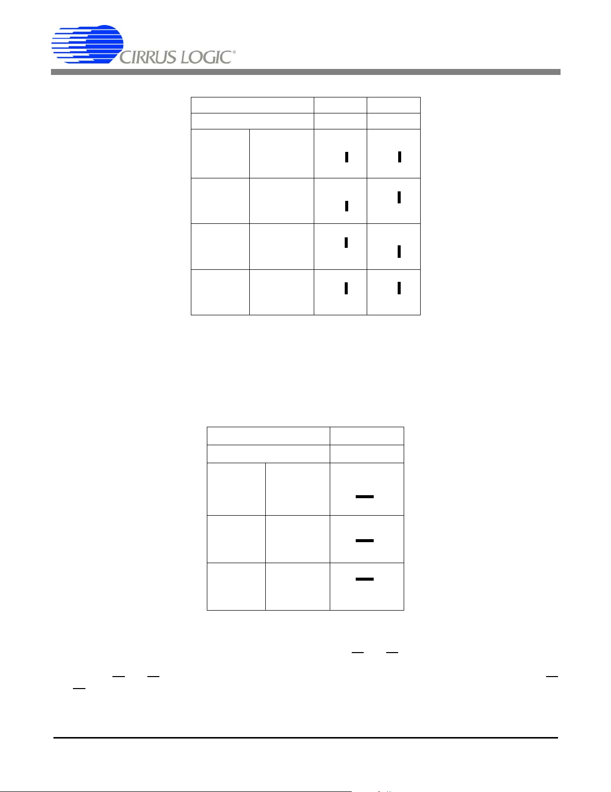
Table 1. Voltage Reference Selection for VREF ............................................................................. 4
Table 2. Voltage Reference Selection for VREF ............................................................................. 4
Table 3. Voltage and Current Channel Input Signal Selection ........................................................ 5
Table 4. Current Channel PGA Selection........................................................................................ 6
Table 5. HPF Option Selection........................................................................................................ 6
Table 6. Energy Output Frequency ................................................................................................. 7
Table 7. Power Supply Connections ...............................................................................................8
2 DS676DB1
Page 3
CDB5466U
1. HARDWARE
1.1 Introduction
The CS5466 is a low cost power measurement solution combining two ∆Σ analog-to-digital converters (ADCs), an
energy-to-frequency converter, and energy pulse outputs on a single chip. It is designed to accurately measure and
calculate energy for single phase, 2- or 3-wire power metering applications with minimal external components.
Low-frequency energy outputs, E1
and E2 supply average active power and can be used to drive a stepper motor
or a mechanical counter; the high-frequency energy output FOUT is designed to assist in calibration; and NEG indicates negative energy.
The CS5466 has configuration pins which allow the selection of pulse output frequency, current channel input range,
and the high-pass filter enable option. The CS5466 also has a power-on reset function which holds the part in reset
until the supply reaches the proper level. The CDB5466U is shipped with a CS5466-ISZ device located at U6.
1.2 Evaluation Board Overview
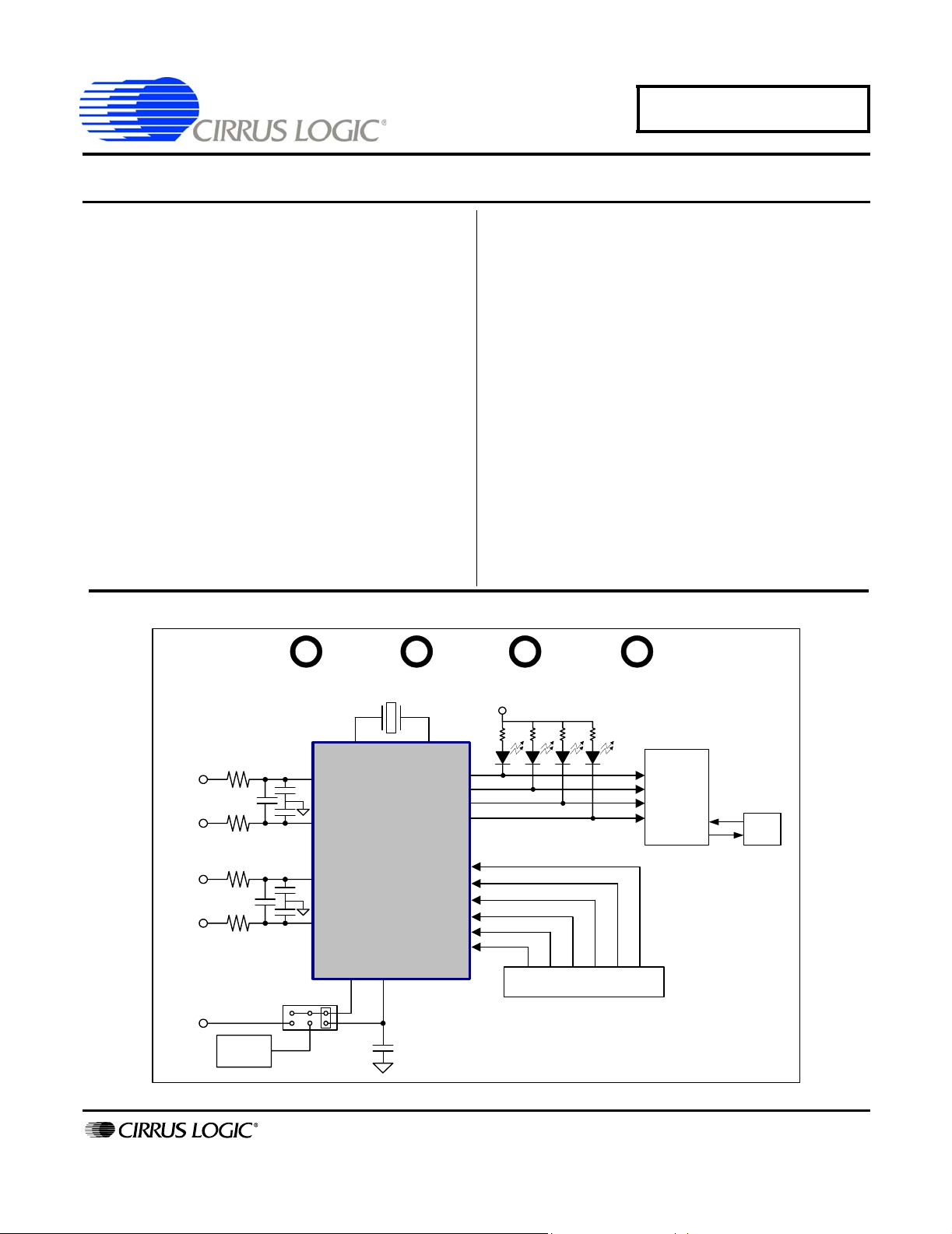
The CDB5466U evaluation board provides a quick path to evaluating the CS5466 Power Measurement IC. Figure
1 illustrates the placement of the terminals, jumpers and IC components. The jumper options are shown in the factory default positions.
TP1 TP2
TP4
TP5
RESET
JP5
GND
JTAG
S1
U3
USB
J1
TP3
8051
LED_EN
1
J10
LED_EN
1
J13
LED_EN
1
J15
LED_EN
1
J16
U5
CS5466 CONFIG
J2
TP6
E1
E2
FOUT
NEG
J32J31J30J29J28
IGAIN0IGAIN1FREQ0FREQ1FREQ2
FOUT
NEG
RESET
HPF
J11
E1
E2
EXT ENER REG
GND
JP4
GND
J33
VD+
FOUT
GND
REF+
GND
GND
VIN+
VIN-
GND
GND
IIN+
IIN-
GND
J14
J23
J27
Vu+_EXTVD+_EXTGND+5V
8051_REGIN
+5V
VD+
J9
J6
JP2
GND
J5J4J3
JP1
GND
GND
VD+
U4
JP3
GND
LT1019
JP6
GND
REF+
GND
VREF
VIN+
VIN-
VREF
GND
GND
VREF
IIN+
IIN-
VREF
GND
J12
J17
J26
J22
J24
VIN+
VIN-
IIN+
IIN-
TP9
TP11
TP12
TP13
CDB5466U REV X
U7
CPUCLK
TP10
J25
VA+
GND VD+GND
VD+_EXT
+5V
+3.3V
XOUT XIN
TP7 TP8
4.096MHz
VREF
VREFIN
VREFOUT
VD+
J8
5466
Vu+_EXT
Y1
Figure 1. CDB5466U Assembly Drawing
DS676DB1 3
Page 4
CDB5466U
The CDB5466U evaluation board is partitioned into two main sections - analog and digital. The analog section consists of the CS5466 and a precision voltage reference that operates from a single +5 V power supply. The digital
section consists of the microcontroller, the reset circuitry, and the USB interface. The digital section can operate from
a +5 V or +3.3 V power supply. The evaluation board is epuipped with power supply connections that accommodate
all of the various supply options of the CS5466.
The evaluation board is designed to output energy-to-pulse conversions upon power-up. Software that runs on a PC
provides a GUI (Graphical User Interface) as a means to quickly register and evaluate the CS5466’s energy-to-pulse
outputs. To accomplish this, the board comes equipped with USB drivers and cable which physically interfaces the
evaluation board to the PC. The software provides easy access to the energy outputs E1
vides a means to display and evaluate the performance of the CS5466.
1.2.1 Analog Section
The CDB5466U evaluation board provides screw-type terminals (J23 and J27) to connect input signals to the voltage and current channels. The screw terminals are labeled as VIN+, VIN-, IIN+, and IIN-. A simple R-C network at
each channel input provides a simple anti-alias filter.
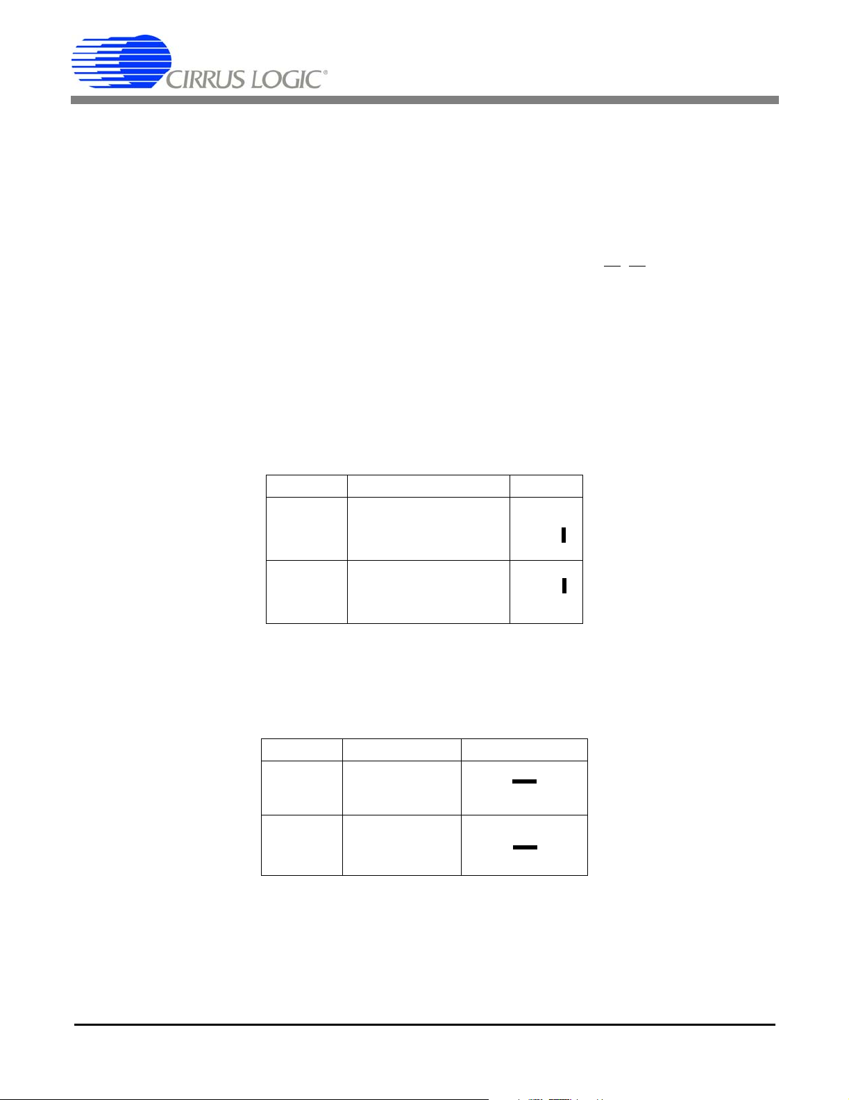
The evaluation board provides three voltage reference options for VREFIN to the CS5466. The three voltage reference options include: VREFOUT from the CS5466, the on-board +2.5 V reference, and external REF+ (screw terminal J14). Table 1 and Table 2 illustrate the options available for VREFIN. With a jumper on J25 in the position
, E2, and FOUT and pro-
Reference Description J25
VREFOUT
VREF
Selects on-Chip
Reference (25ppm/
°C)
Selects External or
LT1019 Reference(J12)
VREFIN
VREFOUT
(Default)
VREFIN
VREFOUT
VREF
O
O
O
O
VREF
Table 1. Internal Voltage Reference Selection for VREF
labeled VREFOUT, the reference is supplied by the on-chip voltage reference. With a jumper on J25 in the position
labeled VREF, the reference is supplied by an off-chip voltage reference.
Table 2 illustrates the options available for VREF. With a jumper on J12 in position LT1019, the LT1019 provides a
Reference Description J12
LT1019
REF+
Selects on-Board
LT1019 Reference
(5ppm/
°C)
Selects External
Reference Source
(J6)
LT1019
REF+
LT1019
REF+
O VREF
O O VREF
O VREF
O O VREF
(Default)
Table 2. External Voltage Reference Selection for VREF
+2.5 V reference (the LT1019 was chosen for its low drift - typically 5ppm/°C). By setting the jumper on J12 to position REF+, an external voltage reference is supplied via screw terminal J14’s REF+ input.
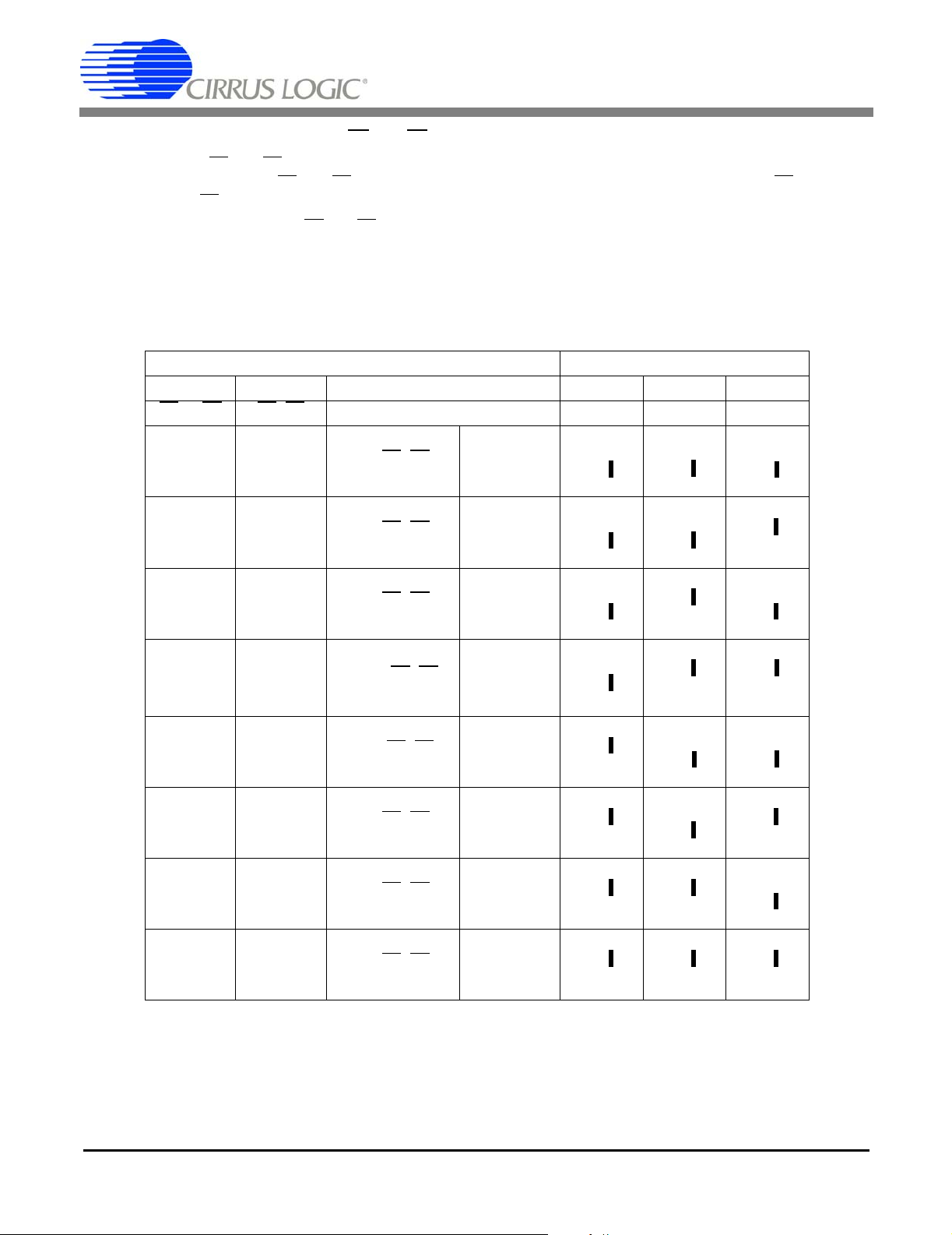
The three input signal options for the voltage (VIN±) and current (IIN±) channel input include: an external signal
(screw terminals J23 and J27), GND or VREF. Table 3 illustrates the options available. By installing jumpers on J17
4 DS676DB1
Page 5
CDB5466U
to position VIN+, J22 to position VN-, J24 to position IIN+ and J26 to position IIN-, the input voltage signal is supplied
from the screw terminals J23 and J27. With a jumper on J17, J22, J24 and J26 in the GND position, the inputs are
connected to analog ground (AGND). With a jumper on J17, J22, J24 and J26 in position
nected to the reference voltage selected on J12.
INPUT Description J17 J22 J24 J26
VREF, the inputs are con-
VIN± or IIN±
VIN± or IIN±
GND
VREFIN
Selects External
Signal
Selects External
Signal
Selects Grounding
the Input
Selects Reference
Source
GND
VREF
VIN+
GND
VREF
VIN+
GND
VREF
VIN+
GND
VREF
VIN+
O VIN+
O O VIN+
O O VIN+
(Default)
O VIN+
O O VIN+
O O VIN+
O VIN+
O O VIN+
O O VIN+
O VIN+
O O VIN+
O O VIN+
VIN-
VREF
GND
VIN-
VREF
GND
VIN-
VREF
GND
VIN-
VREF
GND
O VIN-
O O VIN-
O O VIN-
(Default)
O VIN-
O O VIN-
O O VIN-
O VIN-
O O VIN-
O O VIN-
O VIN-
O O VIN-
O O VIN-
GND
VREF
IIN+
GND
VREF
IIN+
GND
VREF
IIN+
GND
VREF
IIN+
O IIN+
O O IIN+
O O IIN+
(Default)
O IIN+
O O IIN+
O O IIN+
O IIN+
O O IIN+
O O IIN+
O IIN+
O O IIN+
O O IIN+
IIN-
VREF
GND
IIN-
VREF
GND
IIN-
VREF
GND
IIN-
VREF
GND
O IIN-
O O IIN-
O O IIN-
(Default)
O IIN-
O O IIN-
O O IIN-
O IIN-
O O IIN-
O O IIN-
O IIN-
O O IIN-
O O IIN-
Table 3. Voltage and Current Channel Input Signal Selection
1.2.2 Digital Section
The digital section contains the microcontroller, USB interface, JTAG header, reset circuitry, and an external interface header (J11). The microcontroller interfaces the energy pulses, E1
the USB connection to the PC. The microcontroller also provides a hardware reset to the CS5466, which is level
shifted to support both +3.3 V and +5 V digital operation. Interface header, J11, is provided to allow the CDB5466U
to be connected to an external energy registration device. The energy output pins E1
to LEDs which provide a simple visual check of the energy output pulses. Jumpers J10, J13, J15 and J16 are
equipped at the factory with jumpers to enable the LEDs.
, E2, and FOUT output by the CS5466 with
, E2, FOUT and NEG are routed
1.2.2.1 Current Channel Gain
To accommodate different current-sensing elements the current channel incorporates a programmable gain that can
be set to one of four input ranges. Input pins IGAIN1 and IGAIN0 define the four gain selections and corresponding
maximum input signal level. Jumpers J31 and J32 define the state of IGAIN1 and IGAIN0, respectively. Table 4 illustrates the options available. With jumpers J31 = J32 = GND the gain is set to 10x. With jumpers J31 = GND and
J32 = VD+ the gain is set to 50x. With jumpers J31 = VD+ and J32 = GND the gain is set to 100x. With jumpers
J31 = VD+ and J32 = VD+ the gain is set to 150x.
DS676DB1 5
Page 6
Maximum Input Range IGAIN1 IGAIN0
J31 J32
CDB5466U
±250mV 10x
±50mV 50x
±25mV 100x
±16.67mV 150x
VD+
IGAIN1
GND
(Default)
VD+
IGAIN1
GND
VD+
IGAIN1
GND
VD+
IGAIN1
GND
O
O
O
O
O
O
O
O
VD+
IGAIN0
GND
(Default)
VD+
IGAIN0
GND
VD+
IGAIN0
GND
VD+
IGAIN0
GND
O
O
O
O
O
O
O
O
Table 4. Current Channel PGA Selection
1.2.2.2 High-pass Filter
By removing the offset from either channel, no error component will be generated at DC when computing the active
(real) power. Input pin HPF defines the three options, and J33 defines the state of the HPF pin.
– HPF is enabled in the voltage channel when jumper J33 = GND.
– HPF is enabled in the current channel when pin HPF is connected to pin FOUT.
– High-Pass Filter (HPF) is disabled when jumper J33 = VD+.
HPF
High Pass Filter Option J33
Voltage
Channel
Current
Channel
Disabled
HPF Option
is in Voltage
Channel
HPF Option
is in Current
Channel
HPF Option
is Disabled
HPF
HPF
HPF
HPF
HPF
HPF
HPF
HPF
HPF
O O VD+
O O FOUT
O GND
(Default)
O O VD+
O O FOUT
O GND
O O VD+
O O FOUT
O GND
Table 5. HPF Option Selection
1.2.2.3 Energy Pulse Outputs
The CS5466 provides three output pins for energy registration. The E1 and E2 pins provide a simple interface from
which energy can be registered. These pins are designed to directly connect to a stepper motor or electromechanical
counter. The E1
and E2 pins are in the range of 0 to 4 Hz and all frequency settings are optimized to be used with standard meter
constants. The FOUT pin is designated for system calibration, the pulse rate can be selected to reach a frequency
of 8000 Hz. The FOUT output is available on header J11, pin 5.
and E2 outputs are available on header J11, pins 1 and 3, respectively. The pulse rate on the E1
6 DS676DB1
Page 7
CDB5466U
1.2.2.4 Selecting Frequency of E1 and E2
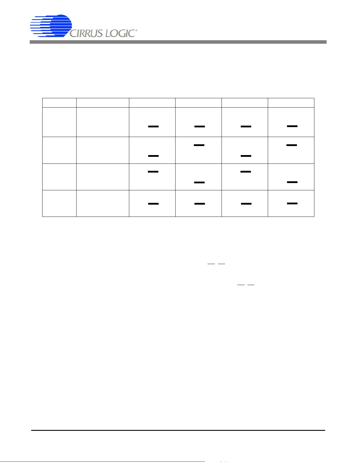
The pulse rate on E1 and E2 can be set to one of four frequency ranges. Input pins FREQ1 and FREQ0 determine
the maximum frequency on E1
the frequency of E1
with active-low alternating pulses. Table 6 illustrates the options available.
The maximum frequency on the E1
J30, if the maximum peak differential signal applied to both channels is a sine wave with zero phase shift.
Maximum Frequency for a Sine Wave Frequency Select
E1
or E2 E1+E2 FOUT J28 J29 J30
and E2 for sine wave inputs with zero phase shift. The frequency of E2 is equal to
and E2 output pins is determined by the position of the jumpers on J28, J29 and
FREQ2 FREQ1 FREQ0
0.125 Hz 0.25 Hz 64x(E1
0.25 Hz 0.5 Hz 32x(E1
0.5Hz 1.0 Hz 16x(E1
1.0 Hz 2.0 Hz 2048x(E1
0.125 Hz 0.25 Hz 128x(E1
0.25 Hz 0.5 Hz 64x(E1
0.5 Hz 1.0 Hz 32x(E1
+E2)16 Hz
VD+
FREQ2
GND
+E2)16 Hz
VD+
FREQ2
GND
+E2)16 Hz
VD+
FREQ2
GND
VD+
+E2) 4,096 Hz
FREQ2
GND
(Default)
+E2)32 Hz
VD+
FREQ2
GND
+E2)32 Hz
VD+
FREQ2
GND
+E2)32 Hz
VD+
FREQ2
GND
O
FREQ1
GND
VD+
O
O
FREQ1
GND
VD+
O
O
FREQ1
GND
VD+
O
O
FREQ1
GND
VD+
O
(Default)
O
FREQ1
GND
VD+
O
O
FREQ1
GND
VD+
O
O
FREQ1
GND
VD+
O
O
O
O
O
O
O
O
O
O
O
O
O
O
O
VD+
FREQ0
GND
VD+
FREQ0
GND
VD+
FREQ0
GND
VD+
FREQ0
GND
(Default)
VD+
FREQ0
GND
VD+
FREQ0
GND
VD+
FREQ0
GND
O
O
O
O
O
O
O
O
O
O
O
O
O
O
1.0 Hz 2.0 Hz 16x(E1
+E2)32 Hz
VD+
FREQ2
GND
O
O
VD+
FREQ1
GND
O
O
VD+
FREQ0
GND
O
O
Table 6. Energy Output Frequency
DS676DB1 7
Page 8

CDB5466U
1.2.3 Power Supply Section
Table 7 illustrates the power supply connections to the evaluation board. The +5 binding post (J3) supplies the positive analog supply (VA+) for the CS5466 and the +2.5 V reference. The VD+_EXT binding post (J5) supplies the
digital section of the CS5466 (VD+) and level shifters. Jumper J8 allows the VD+ supply to be sourced from the
VD+_EXT binding post (J5), the +5 V binding post (J3), or the regulated +3.3 V supply derived from the microcontroller. The Vu+_EXT (J6) binding post supplies the positive supply for the 8051 processor (8051_REGIN). Jumper
J9 allows the 8051_REGIN supply to be sourced from either the Vu+_EXT binding post (J6), +5 V binding post (J3)
or VD+_EXT binding post (J5).
Power Supplies Power Post Connections VD+ 8051-REGIN
Analog (VA+) Digital (VD+) 8051 (Vu+)
+5V GND VD+EXT VU+EXT J8 J9
+5 +5 +5 +5 0
+5 +3.3 +5 +5 0
Table 7. Power Supply Connections
NC
+5
NC
NC
+3.3
NC
+5
NC
NC
+5
NC
+5
NC
+5
VD+_EXT
+5
+3.3
VD+_EXT
+5
+3.3
VD+_EXT
+5
+3.3
VD+_EXT
+5
+3.3
VD+_EXT
+5
+3.3
VD+_EXT
+5
+3.3
VD+_EXT
+5
+3.3
VD+_EXT
+5
+3.3
VD+_EXT
+5
+3.3
VD+_EXT
+5
+3.3
O VD+
O O VD+
O O VD+
(Default)
O VD+
O O VD+
O O VD+
O VD+
O O VD+
O O VD+
O VD+
O O VD+
O O VD+
O VD+
O O VD+
O O VD+
O VD+
O O VD+
O O VD+
O VD+
O O VD+
O O VD+
O VD+
O O VD+
O O VD+
O VD+
O O VD+
O O VD+
O VD+
O O VD+
O O VD+
Vu+_EXT
+5
VD+
Vu+_EXT
+5
VD+
Vu+_EXT
+5
VD+
Vu+_EXT
+5
VD+
Vu+_EXT
+5
VD+
Vu+_EXT
+5
VD+
Vu+_EXT
+5
VD+
Vu+_EXT
+5
VD+
Vu+_EXT
+5
VD+
Vu+_EXT
+5
VD+
O 8051
O O 8051
O O 8051
(Default)
O 8051
O O 8051
O O 8051
O 8051
O O 8051
O O 8051
O 8051
O O 8051
O O 8051
O 8051
O O 8051
O O 8051
O 8051
O O 8051
O O 8051
O 8051
O O 8051
O O 8051
O 8051
O O 8051
O O 8051
O 8051
O O 8051
O O 8051
O 8051
O O 8051
O O 8051
8 DS676DB1
Page 9

CDB5466U
2. SOFTWARE
The evaluation board comes with a USB cable to link the evaluation board to the PC. The evaluation software is
available for download on the Cirrus Logic web site at http://www.cirrus.com/industrialsoftware
run under Windows
®
2000 or Windows® XP.
2.1 Installation Procedure
The CDB5466U is designed to perform active energy measurement and output energy pulse registration upon powering up. Evaluation software is available to aid in registering energy pulse outputs. To install the software, go to the
Cirrus Logic WEB site at http://www.cirrus.com/industrialsoftware
and refer to application note AN278.
2.2 Using the Software
Before launching the evaluation software, check all jumper settings on the CDB5466U evaluation board as described in Section 1, and connect the board to an open USB port on the PC using the provided cable. Once the board
is powered on, the software program can be launched.
2.2.1 Start-Up Window
When the software is launched, the Start-Up window will appear. This window contains information concerning the
software’s title, revision number, copyright date, etc. See Figure 2.
and is designed to
Figure 2. CDB5466U Start-up Window
At the top of the screen is a menu bar which displays user options. The menu bar has three items; Menu, Setup and
Quit. Initially Menu is disabled to prevent conflicts with other serial communications devices. After establishing com-
munication with the CDB5466U evaluation board the Menu item will become available.
DS676DB1 9
Page 10

CDB5466U
2.2.1.1 Setup
Setup presents the communication connections available to the CDB5466U Evaluation Board. The CDB5466U has
one connection option available, USB. As depicted in Figure 2, if the USB setup is selected, the evaluation software
will poll the CDB5466U, verifying the serial communication link is ready. At this point USB is checked indicating that
the PC has successfully communicated with the CDB5466U Evaluation Board.
If the evaluation software is unable to establish a communication link with the CDB5466U a message window will
appear, indicating that the initial communication has failed. See Figure 3.
Figure 3. Alert Window
Check to verify that the USB cable is connected properly and the power supply is on and connected properly to the
CDB5466U.
2.2.1.2 Quit
Quit allows the user to exit the evaluation software. Upon selecting Quit, a message window appears and queries if
exiting the evaluation software is desired. See Figure 4.
Figure 4. Quit Window
10 DS676DB1
Page 11

CDB5466U
2.2.1.3 Menu
Menu allows one selection option, Pulse Rate Window. The Pulse Rate Window provides a means to register the
energy-to-pulse outputs. See Figure 5.
Figure 5. CDB5466 Evaluation Board
Upon selecting Pulse Rate Window, the CS5466 Pulse Rate Output Window will appear.
2.2.2 CS5466 Pulse Rate Output Window
The Pulse Rate Output Window provides a means to access the E1, E2 and FOUT pin of the CS5466. See Figure 6.
Figure 6. CDB5466U Pulse Rate Output Window
DS676DB1 11
Page 12

CDB5466U
In the CS5466 Pulse Rate Output Window, the Pulse Count, Frequency, Average Freq and Standard Deviation are
displayed for the three energy-to-pulse outputs.
Count Span: The Count Span entry allows for a time period to be specified for counting the energy pulses output
by the CS5466. The Count Span is a decimal number having a range of 0.18 < Count Span < 167,772, with units of
seconds.
Periods to Average: The Periods to Average entry allows an average to be performed on the pulses counted during
the specified Count Span. The Periods to Average is an integer with a range of 1 < Periods to Average < 10,000.
Reset DUT: When this button is selected, the evaluation software will request the microcontroller to hardware reset
the CS5466. The CS5466 will perform a reset as discussed in the CS5466 data sheet.
Start/Stop: Initially the Stop button is hidden. When the Start button is selected, the evaluation software will instruct
the microcontroller to start counting the energy-to-pulse outputs from the CS5466. At this time the Start button is
disabled and the Stop button will appear. The evaluation software will then collect the Pulse Count over a duration
of time specified (in seconds) by the Count Span. The counted pulses will then be averaged over the specified Pe-
riods to Average entry. The Pulse Count and calculated Frequency, Average Freq and Standard Deviation will be
displayed at the end of the cycle.
12 DS676DB1
Page 13

3. SCHEMATICS
CDB5466U
Figure 7. Analog Inputs
DS676DB1 13
Page 14
CDB5466U
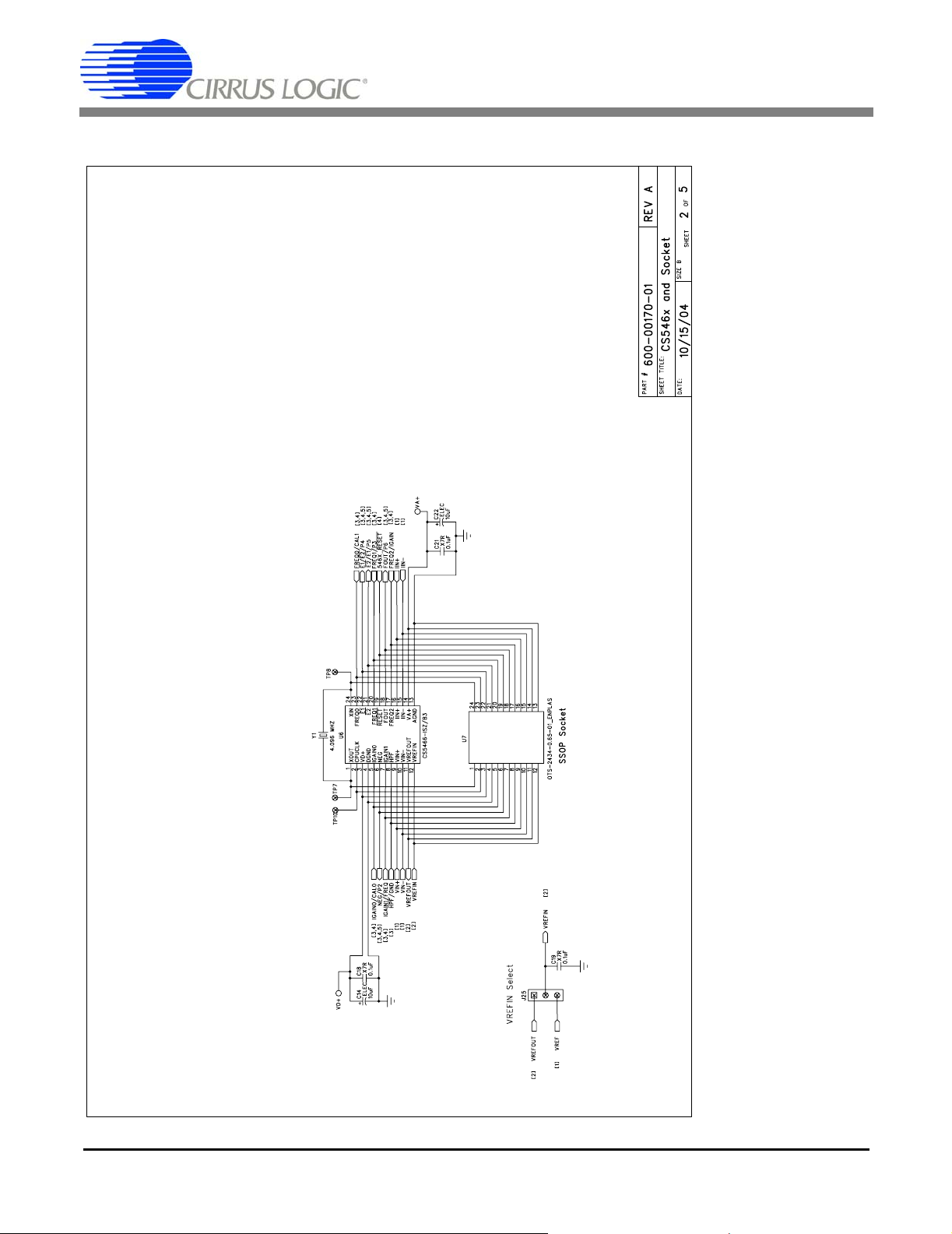
Figure 8. CS546x and Socket
14 DS676DB1
Page 15

CDB5466U
Figure 9. CS5462 and CS5466 Configuration
DS676DB1 15
Page 16

CDB5466U
Figure 10. Microcontroller and USB Interface
16 DS676DB1
Page 17

CDB5466U
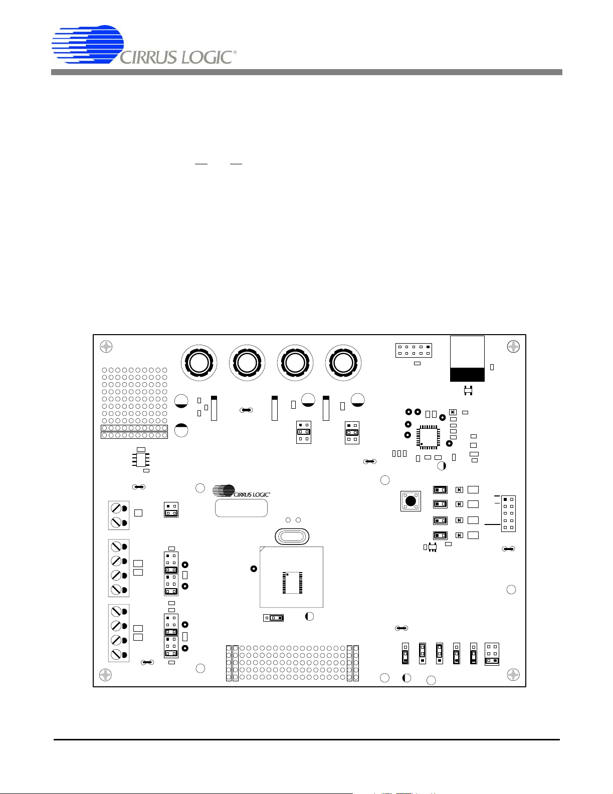
Figure 1. Silk Screen
Figure 11. Power Supply
DS676DB1 17
Page 18

4. LAYOUT
CDB5466U
Figure 1. Topside Layer
18 DS676DB1
Page 19

CDB5466U
Figure 1. Bottomside Layer
DS676DB1 19
Page 20

CDB5466U
20 DS676DB1
Page 21

CDB5466U
Contacting Cirrus Logic Support
For all product questions and inquiries contact a Cirrus Logic Sales Representative.
To find one nearest you go to www.cirrus.com
IMPORTANT NOTICE
Cirrus Logic, Inc. and its subsidiaries ("Cirrus") believe that the information contained in this document is accurate and reliable. However, the information is subject
to change without notice and is provided "AS IS" without warranty of any kind (express or implied). Customers are advised to obtain the latest version of relevant
information to verify, before placing orders, that information being relied on is current and complete. All products are sold subject to the terms and conditions of sale
supplied at the time of order acknowledgment, including those pertaining to warranty, indemnification, and limitation of liability. No responsibility is assumed by Cirrus
for the use of this information, including use of this information as the basis for manufacture or sale of any items, or for infringement of patents or other rights of third
parties. This document is the property of Cirrus and by furnishing this information, Cirrus grants no license, express or implied under any patents, mask work rights,
copyrights, trademarks, trade secrets or other intellectual property rights. Cirrus owns the copyrights associated with the information contained herein and gives consent for copies to be made of the information only for use within your organization with respect to Cirrus integrated circuits or other products of Cirrus. This consent
does not extend to other copying such as copying for general distribution, advertising or promotional purposes, or for creating any work for resale.
CERTAIN APPLICATIONS USING SEMICONDUCTOR PRODUCTS MAY INVOLVE POTENTIAL RISKS OF DEATH, PERSONAL INJURY, OR SEVERE PROPERTY OR ENVIRONMENTAL DAMAGE ("CRITICAL APPLICATIONS"). CIRRUS PRODUCTS ARE NOT DESIGNED, AUTHORIZED OR WARRANTED FOR USE
IN AIRCRAFT SYSTEMS, MILITARY APPLICATIONS, PRODUCTS SURGICALLY IMPLANTED INTO THE BODY, AUTOMOTIVE SAFETY OR SECURITY DEVICES, LIFE SUPPORT PRODUCTS OR OTHER CRITICAL APPLICATIONS. INCLUSION OF CIRRUS PRODUCTS IN SUCH APPLICATIONS IS UNDERSTOOD
TO BE FULLY AT THE CUSTOMER'S RISK AND CIRRUS DISCLAIMS AND MAKES NO WARRANTY, EXPRESS, STATUTORY OR IMPLIED, INCLUDING THE
IMPLIED WARRANTIES OF MERCHANTABILITY AND FITNESS FOR PARTICULAR PURPOSE, WITH REGARD TO ANY CIRRUS PRODUCT THAT IS USED
IN SUCH A MANNER. IF THE CUSTOMER OR CUSTOMER'S CUSTOMER USES OR PERMITS THE USE OF CIRRUS PRODUCTS IN CRITICAL APPLICATIONS, CUSTOMER AGREES, BY SUCH USE, TO FULLY INDEMNIFY CIRRUS, ITS OFFICERS, DIRECTORS, EMPLOYEES, DISTRIBUTORS AND OTHER
AGENTS FROM ANY AND ALL LIABILITY, INCLUDING ATTORNEYS' FEES AND COSTS, THAT MAY RESULT FROM OR ARISE IN CONNECTION WITH
THESE USES.
Cirrus Logic, Cirrus, and the Cirrus Logic logo designs are trademarks of Cirrus Logic, Inc. All other brand and product names in this document may be trademarks
or service marks of their respective owners.
Windows is a registered trademark of Microsoft Corporation.
DS676DB1 21
 Loading...