

Page 1
CDB5463U
CDB5463U Engineering Board and GUI Software
Features
Voltage and Current Interface
USB Communication with PC
On-board C8051F320 Microcontroller
On-board Voltage Reference
LabWindows
– Register Setup & Chip Control
– FFT Analysis
– Time Domain Analysis
– Noise Histogram Analysis
"Auto-boot" Demo with Serial EEPROM
®
/CVI® GUI Software
General Description
The CDB5463U is an inexpensive tool designed to evaluate
the functionality and performance of the CS5463 analog-to-digital converter (ADC). The evaluation board includes an LT1019
voltage reference, a C8051F320 microcontroller with a USB interface, and firmware. The microcontroller controls the serial
communication between the evaluation board and the PC via
the firmware, enabling quick and easy access to all of
theCS5463's registers and functions.
The CDB5463U includes software for data capture, time domain analysis, histogram analysis, and frequency domain
analysis.
Schematics in PADS™ PowerLogic™ format are available for
download at www.cirrus.com/IndustrialSoftware
ORDERING INFORMATION
CDB5463U Evaluation Board
.
REF
VIN+
VIN-
IIN+
IIN-
www.cirrus.com
+2.5V
reference
+5V GND
IN OUT
VREF
CS5463
4.096MHz
Crystal
Copyright © Cirrus Logic, Inc. 2007
VD+_EXT
EERPOM
CS
SDI
SDO
SCLK
INT
RESET
E1
E2
E3
MODE
(All Rights Reserved)
Vu+_EXT
SERIAL
C8051F320
Reset
Circuirty
RESET
BUTTON
USB
OCT ‘07
DS805DB2
Page 2

CDB5463U
TABLE OF CONTENTS
1. HARDWARE ............................................................................................................................. 3
1.1 Introduction ........................................................................................................................ 3
1.2 Evaluation Board Overview ................................................................................................ 3
1.3 Analog Section ................................................................................................................... 4
1.4 Digital Section .................................................................................................................... 5
1.5 Power Supply Section ........................................................................................................ 5
1.6 Auto-boot Mode ................................................................................................................. 6
2. SOFTWARE .............................................................................................................................. 8
2.1 Installation .......................................................................................................................... 8
2.2 Using the Software ............................................................................................................. 8
2.3 Start-up Window ................................................................................................................ 8
2.4 Setup Window .................................................................................................................. 12
2.5 Calibration Windows ........................................................................................................14
2.6 Conversion Window ......................................................................................................... 16
2.7 Pulse Rate Window ..........................................................................................................18
2.8 Data Collection Window ................................................................................................... 19
2.9 EEPROM Window ............................................................................................................ 26
2.10 Debug Panel .................................................................................................................. 27
Appendix A. Bill Of Materials ................................................................................................... 28
Appendix B. Schematics .......................................................................................................... 30
Appendix C. Layer Plots ........................................................................................................... 34
LIST OF FIGURES
Figure 1. CDB5463U Assembly Drawing ........................................................................................ 3
Figure 2. GUI Start-up Window ....................................................................................................... 8
Figure 3. Setup Menu Showing Successful USB Connection ......................................................... 9
Figure 4. USB Error Message ......................................................................................................... 9
Figure 5. Data from Disc File Selection Window ........................................................................... 10
Figure 6. Menu Pull-down Options ................................................................................................11
Figure 7. Quit Dialog ..................................................................................................................... 11
Figure 8. Setup Window ................................................................................................................ 12
Figure 9. Calibration Window ........................................................................................................ 14
Figure 10. Conversion Window ..................................................................................................... 16
Figure 11. Pulse Rate Output Window .......................................................................................... 18
Figure 12. Data Collection Window ...............................................................................................19
Figure 13. Configuration Window .................................................................................................. 20
Figure 14. Histogram Analysis ...................................................................................................... 22
Figure 15. FFT Analysis ................................................................................................................ 24
Figure 16. Time Domain Analysis .................................................................................................25
Figure 17. EEPROM Window........................................................................................................26
Figure 18. Debug Panel ................................................................................................................ 27
Figure 19. Schematic - Analog Inputs ........................................................................................... 30
Figure 20. Schematic - CS5463 & Socket..................................................................................... 31
Figure 21. Schematic - Microcontroller & USB Interface ............................................................... 32
Figure 22. Schematic - Power Supplies ........................................................................................ 33
Figure 23. Top Silkscreen ............................................................................................................. 34
Figure 24. Top Routing.................................................................................................................. 35
Figure 25. Bottom Routing ............................................................................................................ 36
Figure 26. Bottom Silkscreen ........................................................................................................ 37
2 DS805DB2
Page 3
CDB5463U
1. HARDWARE
1.1 Introduction
The CDB5463U evaluation board provides a convenient means of evaluating the CS5463 power measurement IC. The CDB5463U evaluation board operates from a single +5V power supply. The evaluation
board interfaces the CS5463 to a PC via a USB cable. To accomplish this, the board comes equipped
with a C8051F320 microcontroller and a USB interface. Additionally, the CDB5463U GUI software provides easy access to the internal registers of the CS5463. The software also provides a means to display
the performance in the time domain or frequency domain.
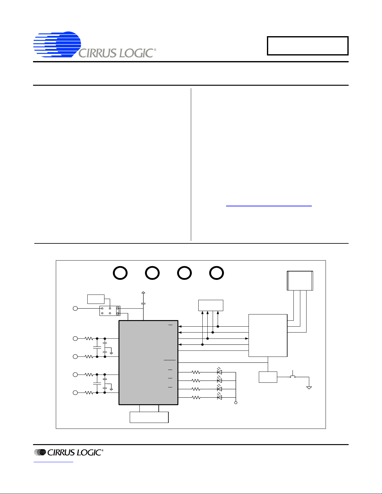
1.2 Evaluation Board Overview
The board is partitioned into two main sections: analog and digital. The analog section consists of the
CS5463 and a precision voltage reference. The digital section consists of the C8051F320 microcontroller,
EEPROM, the hardware test switches, the reset circuitry, and the USB interface. The board also has a
user friendly power supply connection.
REF+
GND
GND
VIN+
VIN-
GND
GND
IIN+
IIN-
GND
J14
J23
J27
U4
JP3
GND
LT1019
JP6
GND
TP2
REF+
GND
VREF
VIN+
VIN-
VREF
GND
GND
VREF
IIN+
IIN-
VREF
GND
GND
VD+
J12
J17
VIN+
VINJ22
J24
IIN+
J26
IIN-
CDB5460A_61A_63
TP9
TP11
TP12
TP13
J5J4J3
JP1
GND
CDB5463U
CPUCLK
TP10
XU6
VD+
VD+_EXT
+5V
+3.3V
J8
XOUT XIN
TP7 TP8
4.096MHz
U6
Vu+_EXT
Y1
5463
J25
VREF
VREFIN
VA+
GND VD+GND
VREFOUT
Vu+_EXTVD+_EXTGND+5V
8051_REGIN
+5V
VD+
J9
TP30
PFMON
TP23
TP22
TP21
TP25
TP20
JTAG
TP24
S1
RESET
J6
JP2
GND
TP26
U3
U11
USB
J1
J2
U1
JP4
D1
EVENT
TP27
ERROR
8051
LED_EN
1
J10
LED_EN
1
J13
LED_EN
1
J15
LED_EN
MODE
1
J16
1
J18
AUTO-BOOT
ENABLE
U9
U10
JP5
GND
U8
GND
TP1
E1
E2
E3
U5
RESET
MODE
EECS
SCLK
MISO
MOSI
U2
INT
CS
E1
E2
E3
J40
1
21 22
2
Figure 1. CDB5463U Assembly Drawing
DS805DB2 3
Page 4
CDB5463U
1.3 Analog Section
The CDB5463U evaluation board provides screw-type terminals (J23, J27) to connect input signals to the
voltage and current channels. The screw terminals are labels as VIN+, VIN1-, IIN+, and IIN-. A simple
R-C network at each channel input provides a simple anti-alias filter.
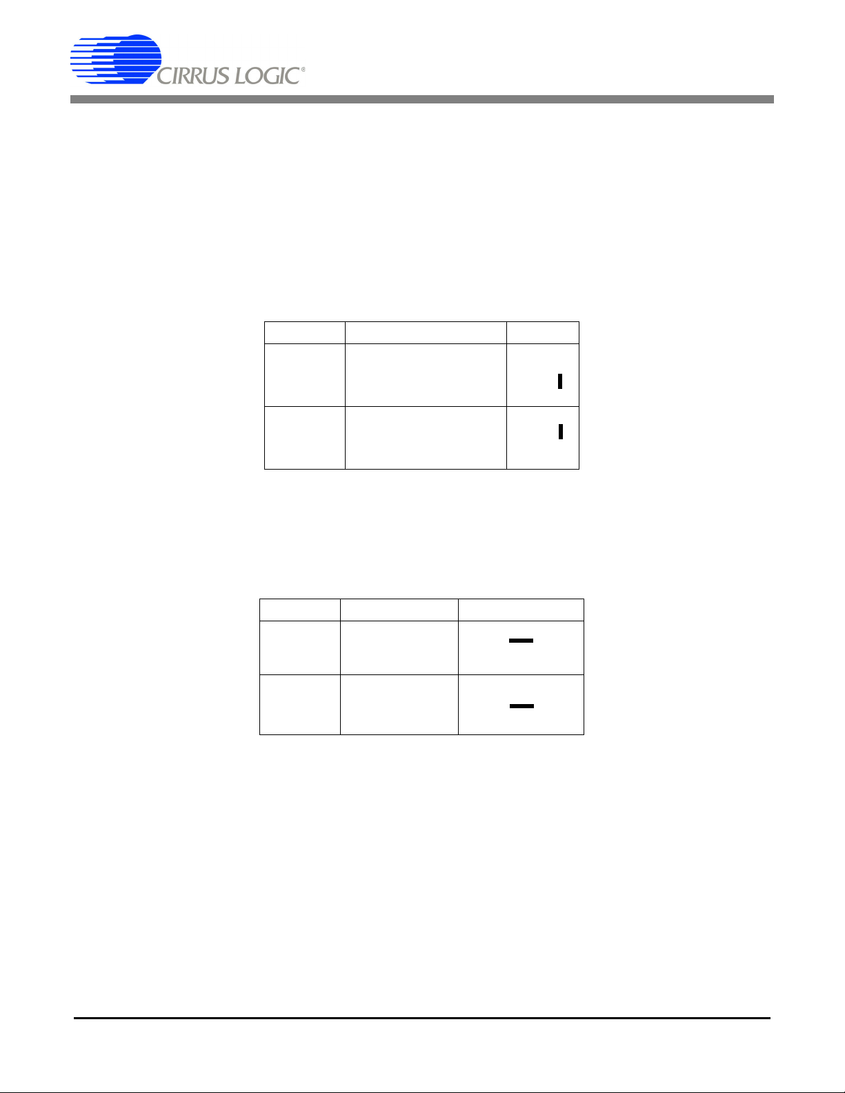
The evaluation board provides three voltage reference options for VREFIN to the CS5463. The three voltage reference options include: VREFOUT from CS5463, the on-board +2.5V reference, and external
REF+ (screw terminal J14).
on J25 in the position labeled VREFOUT, the reference is supplied by the on-chip voltage reference. With
a jumper on J25 in the position labeled VREF, the reference is supplied by an off-chip voltage reference.
Table 1 and Table 2 illustrate the options available for VREFIN. With a jumper
Reference Description J25
VREFOUT
VREF
Selects On-chip
Reference (25 ppm/
°C)
Selects External or
LT1019 Reference(J12)
VREFIN
VREFOUT
(Default)
VREFIN
VREFOUT
VREF
O
O
O
O
VREF
Table 1. Internal Voltage Reference Selection for VREF
Table 2 illustrates the options available for VREF. With a jumper on J12 in position LT1019, the LT1019
provides a +2.5V reference (the LT1019 was chosen for its low drift - typically 5 ppm/°C). By setting the
jumper on J12 to position REF+, an external voltage reference is supplied via screw terminal J14's REF+
input.
Reference Description J12
LT1019
REF+
Selects On-board
LT1019 Reference
(5 ppm/
°C)
Selects External
Reference Source
(J14)
LT1019
REF+
LT1019
REF+
O VREF
O O VREF
O VREF
O O VREF
(Default)
Table 2. External Voltage Reference Selection for VREF
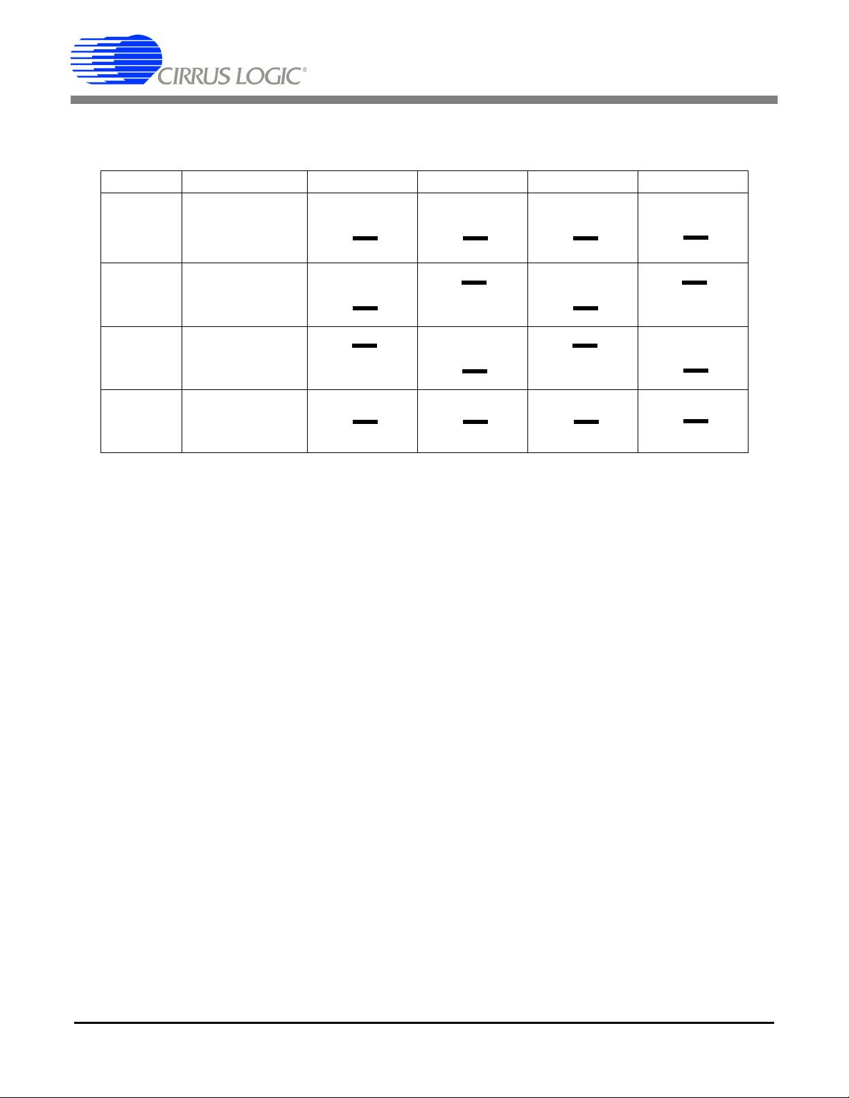
The three input signal options for the voltage (VIN±) and current (IIN±) channel input include: an external
signal (screw terminals J23 and J27), GND, or VREF. Table3 illustrates the options available. By installing
jumpers on J17 to position VIN+, J22 to position VIN-, J24 to position IIN+, and J26 to position IIN-, the
input voltage signal is supplied from the screw terminals J23 and J27. With a jumper on J17, J22, J24 and
4 DS805DB2
Page 5
CDB5463U
J26 in the GND position, the inputs are connected to analog ground (AGND). With a jumper on J17, J22,
J24 and J26 in position VREF, the inputs are connected to the reference voltage selected on J12.
INPUT Description J17 J22 J24 J26
VIN± or IIN±
VIN± or IIN±
GND
VREFIN
Selects External
Signal
Selects External
Signal
Selects Grounding
the Input
Selects Reference
Source
GND
VREF
VIN+
GND
VREF
VIN+
GND
VREF
VIN+
GND
VREF
VIN+
O VIN+
O O VIN+
O O VIN+
(Default)
O VIN+
O O VIN+
O O VIN+
O VIN+
O O VIN+
O O VIN+
O VIN+
O O VIN+
O O VIN+
VIN-
VREF
GND
VIN-
VREF
GND
VIN-
VREF
GND
VIN-
VREF
GND
O VIN-
O O VIN-
O O VIN-
(Default)
O VIN-
O O VIN-
O O VIN-
O VIN-
O O VIN-
O O VIN-
O VIN-
O O VIN-
O O VIN-
GND
VREF
IIN+
GND
VREF
IIN+
GND
VREF
IIN+
GND
VREF
IIN+
O IIN+
O O IIN+
O O IIN+
(Default)
O IIN+
O O IIN+
O O IIN+
O IIN+
O O IIN+
O O IIN+
O IIN+
O O IIN+
O O IIN+
IIN-
VREF
GND
IIN-
VREF
GND
IIN-
VREF
GND
IIN-
VREF
GND
O IIN-
O O IIN-
O O IIN-
(Default)
O IIN-
O O IIN-
O O IIN-
O IIN-
O O IIN-
O O IIN-
O IIN-
O O IIN-
O O IIN-
Table 3. Voltage and Current Channel Input Signal Selection
1.4 Digital Section
The digital section contains the microcontroller, USB interface, JTAG header, reset circuitry, and an external interface header (J40). The microcontroller interfaces the SPI of CS5463 with the USB connection
to the PC, enabling the GUI software to access all the CS5463 registers and functions. Interface header,
J40, is provided to allow the CDB5463U to be connected to an external energy registration device or an
external microcontroller. To connect the CS5463 to an external microcontroller, R57, R58, R59, R60, R61,
and R62 must be removed from the board. The energy output pins E1, E2, and E3 are routed to LEDs
which provide a simple visual check of the energy output pulses. The MODE pin is also routed to a LED
to indicate whether the CS5463 is operating in auto-boot mode. Jumpers J10, J13, J15, and J16 are
equipped at the factory with jumpers to enable the LEDs.
1.5 Power Supply Section
Table 4 illustrates the power supply connections to the evaluation board. The +5V binding post (J3) sup-
plies the positive analog (VA+) for the CS5463 and the +2.5V reference. The VD+_EXT binding post (J5)
supplies the digital section of the CS5463 (VD+) and level shifters. Jumper J8 allows the VD+ supply to
be sourced from the VD+_EXT binding post (J5), the +5V binding post (J3), or the regulated 3.3V supply
derived from the microcontroller. The Vu+_EXT (J6) binding post supplies the positive supply for the 8051
DS805DB2 5
Page 6
CDB5463U
microcontroller (8051_REGIN). Jumper J9 allows the 8051_REGIN supply to be sourced from either the
Vu+_EXT binding post (J6), +5V binding post (J3) or VD+_EXT binding post (J5).
Power Supplies Power Post Connections VD+ 8051-REGIN
Analog (VA+) Digital (VD+) 8051 (Vu+)
+5V GND VD+EXT VU+EXT J8 J9
+5 +5 +5 +5 0
+5 +3.3 +5 +5 0
Table 4. Power Supply Connections
NC
+5
NC
NC
+3.3
NC
+5
NC
NC
+5
NC
+5
NC
+5
VD+_EXT
+5
+3.3
VD+_EXT
+5
+3.3
VD+_EXT
+5
+3.3
VD+_EXT
+5
+3.3
VD+_EXT
+5
+3.3
VD+_EXT
+5
+3.3
VD+_EXT
+5
+3.3
VD+_EXT
+5
+3.3
VD+_EXT
+5
+3.3
VD+_EXT
+5
+3.3
O VD+
O O VD+
O O VD+
(Default)
O VD+
O O VD+
O O VD+
O VD+
O O VD+
O O VD+
O VD+
O O VD+
O O VD+
O VD+
O O VD+
O O VD+
O VD+
O O VD+
O O VD+
O VD+
O O VD+
O O VD+
O VD+
O O VD+
O O VD+
O VD+
O O VD+
O O VD+
O VD+
O O VD+
O O VD+
Vu+_EXT
+5
VD+
Vu+_EXT
+5
VD+
Vu+_EXT
+5
VD+
Vu+_EXT
+5
VD+
Vu+_EXT
+5
VD+
Vu+_EXT
+5
VD+
Vu+_EXT
+5
VD+
Vu+_EXT
+5
VD+
Vu+_EXT
+5
VD+
Vu+_EXT
+5
VD+
O 8051
O O 8051
O O 8051
(Default)
O 8051
O O 8051
O O 8051
O 8051
O O 8051
O O 8051
O 8051
O O 8051
O O 8051
O 8051
O O 8051
O O 8051
O
8051
O O 8051
O O 8051
O 8051
O O 8051
O O 8051
O 8051
O O 8051
O O 8051
O 8051
O O 8051
O O 8051
O 8051
O O 8051
O O 8051
1.6 Auto-boot Mode
With a jumper connection on J18 (AUTO-BOOT ENABLE), the CS5463 operates in auto-boot mode and
the CDB5463U board operates as a stand-alone system without attaching it up to a PC. When in autoboot mode, a hardware reset (press on S1) will cause the CS5463 to boot up using the serial data from
the serial EEPROM on the board (U10). When the CS5463 is in auto-boot mode, the SPI connections
6 DS805DB2
Page 7

CDB5463U
between the microcontroller and the CS5463 are removed and the GUI software can not access the
CS5463 registers and functions.
The EEPROM must be programmed prior to the auto-boot sequence. When the CDB5463U Evaluation
Board is sent from the factory, the EEPROM is programmed with the following CS5463 command/data
sequence:
1. Write Mode register, turn high-pass filters on:
0x64 0x00 0x00 0x60
2.
Unmask bit #2 (LSD) in the Mask register:
0x74 0x00 0x00 0x04
3.
Start continuous conversion:
0xE8
4.
Write STOP bit to Control register, to terminate auto-boot sequence:
0x78 0x00 0x01 0x00
This sequence programs the CS5463 for continuous conversion mode. If voltage and current signals are
applied to the inputs, the CS5463 will issue pulses on the E1
details on auto-boot.
pin. See the CS5463 data sheet for more
DS805DB2 7
Page 8
2. SOFTWARE
CDB5463U
The evaluation board comes with software and an USB cable to link the evaluation board to the PC. The
evaluation software was developed with LabWindows
tional Instruments. The evaluation software is available for download on the Cirrus Logic web site at
http://www.cirrus.com/industrialsoftware
Windows XP
®
.
and was designed to run under Windows®2000 or
®
/CVI®, a software development package from na-
2.1 Installation
To install the software, go to the Cirrus Logic web site at http://www.cirrus.com/industrialsoftware and re-
fer to application note AN278.
2.2 Using the Software
Before launching the software, check all jumper settings on the CDB5463U evaluation board as described
in Section 1, and connect the board to an open USB port on the PC using the provided cable. Once the
board is powered on, the software program can be launched.
2.3 Start-up Window
When the software is launched, the start-up window will appear. This window contains information concerning the software's title, revision number, copyright date, etc. See Figure 2.
Figure 2. GUI Start-up Window
At the top of the screen is a menu bar which displays user options. The menu bar has three items: Menu,
Setup, and Quit. Initially Menu is disabled. After establishing a link to a data source, the Menu item will
become available.
8 DS805DB2
Page 9
CDB5463U
2.3.1 Setup Menu
Setup allows user to establish a USB communication connection with CDB5463U board or select a previously saved data file for further analysis.
If the USB item in the Setup menu is selected, the evaluation software will poll the CDB5463U, verifying
the serial communication link is ready. At this point, the USB menu item is checked indicating that the PC
has successfully communicated with CDB5463U evaluation board, and device and micro-code version
information are read from the board and displayed on the screen. See Figure 3. Due to improvements to
the software or new features being added, the version displayed may be different than the image shown
here.
Figure 3. Setup Menu Showing Successful USB Connection
If the evaluation software is unable to establish a communication link with the CDB5463U board, a message will appear, indicating that the initial communication has failed. See Figure 4.
Figure 4. USB Error Message
Check to verify that the USB cable is connected properly and the power supply is on and connected properly to the CDB5463U. Reset the board (press the RESET button on the board) and try to setup the USB
connection again.
DS805DB2 9
Page 10
CDB5463U
If the Data from Disk item in the Setup menu is selected, a file selection window will appear as shown in
Figure 5. User can select a pre-saved data file for further analysis using time domain, FFT, and histogram
plots in Data Collection Window of the software.
Figure 5. Data from Disc File Selection Window
2.3.2 Menu Menu
Excluding the Start-Up window, the Menu menu provides 7 options: Setup Window, Calibration Window,
Conversion Window, Pulse Rate Window, Data Collection Window, EEPROM Window, and Debug Win-
10 DS805DB2
Page 11
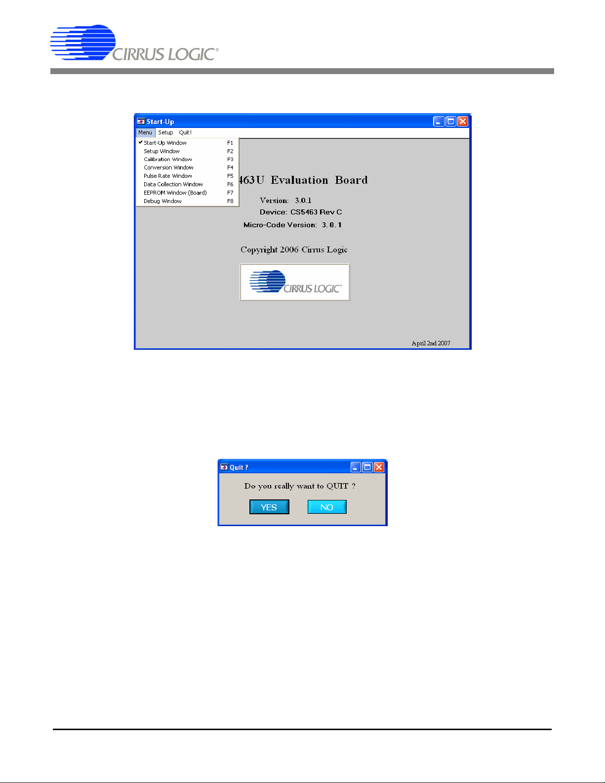
CDB5463U
dow. Each window provides a means to evaluate the different functions and performance of the CS5463.
Each option has an associated function key (<F1>, <F2>, etc.). See Figure 6.
Figure 6. Menu Pull-down Options
2.3.3 Quit Menu
The Quit menu allows the user to exit the evaluation software. Upon selecting Quit, a message window
appears and queries if exiting the evaluation software is desired. See Figure 7.
Figure 7. Quit Dialog
DS805DB2 11
Page 12
CDB5463U
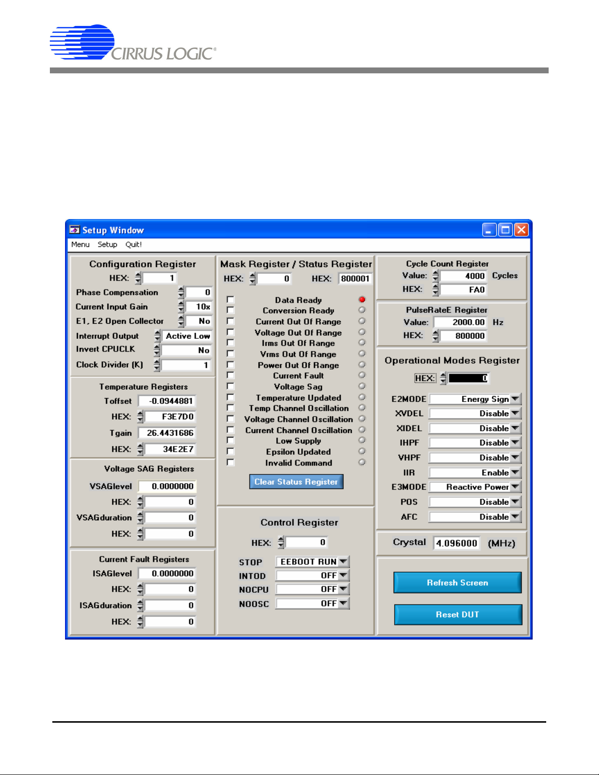
2.4 Setup Window
The evaluation software provides access to the CS5463's internal registers through the Setup window.
See Figure 8. The user can enter the Setup window by pulling down the Menu menu and selecting Setup
Window, or by pressing <F2> on the keyboard.
In the Setup window, all of the CS5463's registers are displayed in hexadecimal notation and are decoded
to provide easier readability. Refer to the CS5463 data sheet for information on register functionality and
definitions. See Figure 8.
Figure 8. Setup Window
12 DS805DB2
Page 13

CDB5463U
2.4.1 Refresh Screen Button
The Refresh Screen button will update the contents of the screen by reading all the register values from
the CS5463. It is a good idea to press the Refresh Screen button when entering the Setup window, or
after modifying any registers, to reflect the current status of the CS5463.
2.4.2 Reset DUT Button
The Reset DUT button will hardware reset the CS5463. The CS5463 will perform a reset as discussed in
the CS5463 data sheet. After the hardware reset to the CS5463 device, the screen contents will be automatically refreshed with the updated status of the CS5463.
2.4.3 CS5463 Crystal Frequency
The CS5463 accepts a wide range of crystal input frequencies, and can therefore run at many different
sample rates. The crystal frequency being used on the CS5463 should be entered in this field to provide
accurate frequency calculation in the FFT window. This will also help the software decide which functions
the evaluation system can perform reliably.
2.4.4 Configuration Register
In the Configuration Register box, the contents of the Config register can be modified by typing a hexadecimal value in the HEX: field, or by changing any of the values below the HEX: field to the desired settings. Although the CDB5463U software allows the user to modify any of the bits in the Config register,
changing certain bits may cause the software and board to behave erratically. For the evaluation system
to function properly, the Interrupt Output field should be set to the default Active Low. This applies only to
the CDB5463U evaluation system, and not to the CS5463 chip itself.
2.4.5 Temperature, Voltage SAG, Current Fault Registers
These fields display the values of the corresponding registers in both hexadecimal and decimal format.
Each register can be modified by typing a value in the corresponding offset, level, duration, or gain value
field (decimal) or HEX: field (hexadecimal).
2.4.6 Mask Register / Status Register
The Mask Register / Status Register box displays the values for these registers in hexadecimal and decodes them to indicate each bit's function. The Mask register can be modified by typing a value in the
HEX: field, or by checking the appropriate check boxes for the bits that are to be masked. The Status register cannot be directly modified. It can only be reset by pressing the Clear Status Register button. The
HEX: field for this register and the lamps are indicators only. A lamp which is on means that the corresponding bit in the Status register is set (except the Invalid Command bit, which is inverted). The value
present in the Mask register may be changed by the software during certain operations to provide correct
functionality of the CDB5463U board.
2.4.7 Cycle Count / PulseRateE Register
These fields display the values of the corresponding registers in both hexadecimal and decimal format.
Each register can be modified by typing a value in the corresponding Value: or HEX: field.
DS805DB2 13
Page 14

CDB5463U
2.4.8 Control Register
The Control Register box contains various bits used to activate or terminate various features of the
CS5463. Refer to the CS5463 data sheet for descriptions of the bits. The user is able to turn each bit on
or off individually. The value of the Ctrl register is displayed in the HEX: field. Most of the Ctrl register bits
are reserved or unused. Only the usable bits are displayed in the Setup window.
2.4.9 Operational Modes Register
The Operational Modes Register box contains various bits used to set different operation modes for the
CS5463 functions. Refer to the CS5463 data sheet for descriptions of the bits. The value of the Mode register is displayed in the HEX: field. Many of the Mode register bits are reserved or unused. Only the usable
bits are displayed in the Setup window.
2.5 Calibration Windows
The Calibration window is used to display and write to the CS5463 offset and gain calibration registers.
The user is also able to initiate the CS5463's calibration sequences that are used to set the calibration
values. Both AC and DC calibrations can be performed for offset and gain, for either the voltage channel
or the current channel, or both simultaneously. The user should refer to the CS5463 data sheet for more
details on calibration.
The Refresh Screen button will update the contents of the screen by reading all the register values from
the CS5463. It is a good idea to press the Refresh Screen button when entering the Calibration window,
or after modifying any registers to reflect the current status of the CS5463.
Figure 9. Calibration Window
14 DS805DB2
Page 15

CDB5463U
2.5.1 Offset / Gain Register
In the Offset & Gain fields, the offset and gain registers for both channels are displayed in hexadecimal
and decimal formats. These registers can be modified directly by typing the desired value in the hexadecimal display fields. There are two types of offset registers: DC offset and AC offset. The AC Offset register
only affects the RMS register values. The DC & AC offset registers are two's complement numbers whose
values ranges from -1 to +1. The gain register value ranges from 0 to 4.
2.5.2 Performing Calibrations
Offset and gain calibrations can be performed on both the voltage and current channels of the CS5463.
Because the initial values in the calibration registers will affect the results of the calibrations, it is generally
a good idea to software reset the CS5463 before running calibrations. A software reset will reset these
registers back to the default values of zero offset and unity gain. Offset calibration should be performed
before gain calibration to ensure accurate results.
2.5.2.1 Offset Calibrations
1. Ground the channel(s) you want to calibrate directly at the channel header(s) J17 and J22 for the voltage
channel, and J24 and J26 for the current channel. The channel(s) could also be grounded directly at the
screw terminals.
2. Press the corresponding AC or DC offset calibrate button (Cal V, Cal I, or Cal Both) beside or below the
corresponding offset registers fields.
The calibration value(s) will automatically update when the calibration is completed.
2.5.2.2 Gain Calibrations
1. Attach an DC or AC calibration signal to the screw terminals, and make sure the corresponding channel
headers (J17, J22, J24, and J26) are set to the input position.
2. Press the corresponding AC or DC gain calibrate button (Cal V, Cal I, or Cal Both) beside or below the Gain
Registers fields.
The calibration value(s) will automatically update when the calibration is completed.
The Calibration Window also contains the Power Offset Register display and adjustment. The user can
read and write the value in the power offset (Poff) register.
DS805DB2 15
Page 16
CDB5463U
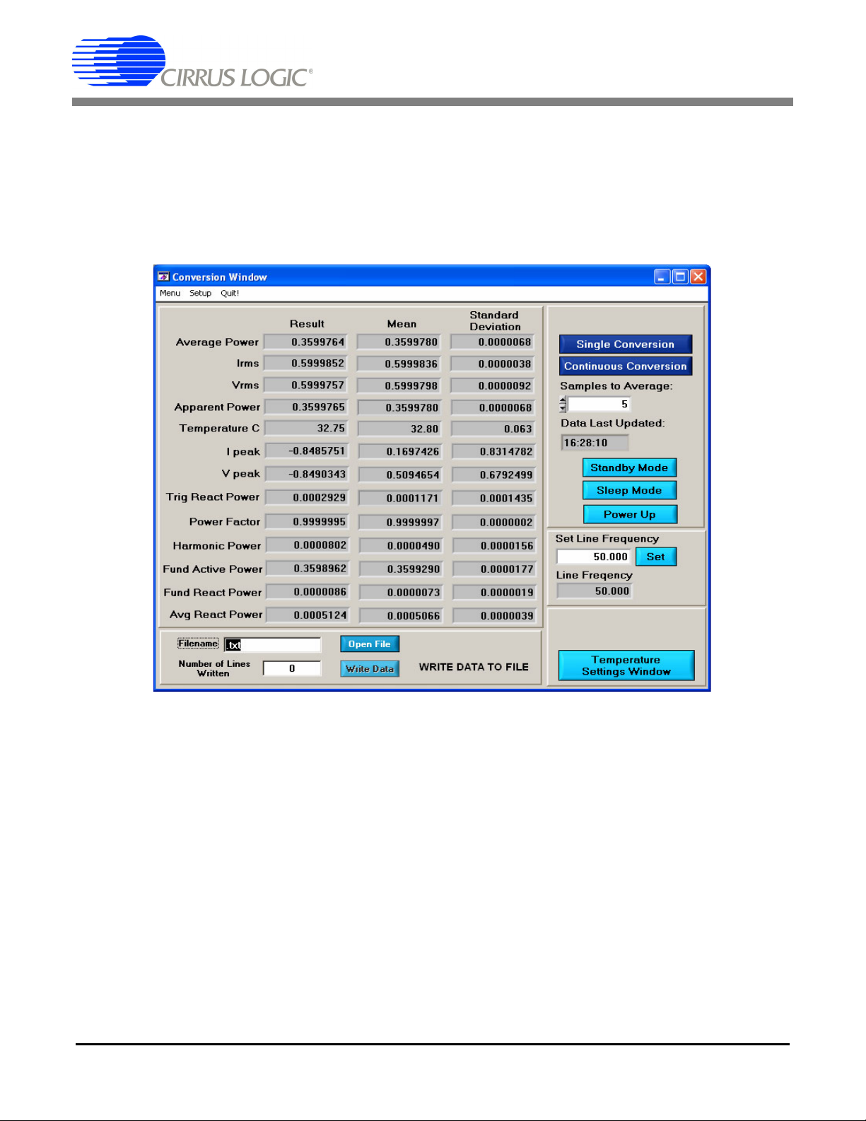
2.6 Conversion Window
The Conversion Window allows the user to see the results of single and continuous conversions, perform
data averaging, and utilize the power-saving modes of the CS5463. See Figure 10. The Conversion Window can be accessed by pulling down the Menu option, and selecting Conversion Window, or by pressing
F4.
Figure 10. Conversion Window
2.6.1 Single Conversion Button
Pressing this button will cause a single conversion to be performed. After a single conversion is complete,
the Result column will be updated with the values present in each data register.
2.6.2 Continuous Conversion Button
Pressing this button will cause continuous conversions to be performed until the user presses the Stop
button. After each conversion is complete, the Result column will be updated with the values present in
each data register. The Mean and Standard Deviation columns will be updated every N cycles, where N
is the number in the Samples to Average field. If the Samples to Average is set to a large number, it may
take many collection cycles after pressing the Stop button before the data actually stops being collected.
16 DS805DB2
Page 17

CDB5463U
2.6.3 Standby / Sleep Mode Buttons
When these buttons are pressed, the CS5463 will enter either standby or sleep power saving modes. To
return to normal mode, press the Power Up button.
2.6.4 Power Up Button
This button is used to send the Power Up/Halt command to the CS5463. The part will return to normal
operating mode and halt any conversions that are being done at this time.
2.6.5 Temperature Settings Window
The Temperature Settings Window is used to adjust the temperature offset register (Toffset) and temperature gain register (Tgain) to convert the temperature register (T) from a Celsius scale (°C) to a Fahrenheit
scale (°F) or vice versa and to improve temperature measurement accuracy. Refer to the CS5463 data
sheet for the details of the on-chip temperature sensor.
2.6.6 Write Data to File Window
This window provides a means to write the conversion result data to a .txt text file for later analysis or
print out. The file path and name will be shown in Filename field. The Open File button is used to open a
new or existing .txt text file for data writing. Each time the Write Data button is pressed, the result data is
written into the file and the Number of Lines Written field value will be increased by 1.
DS805DB2 17
Page 18

CDB5463U
2.7 Pulse Rate Window
The CS5463 features a pulse-rate energy output. The CDB5463U has the capability to demonstrate the
functionality of this output in the Pulse Rate Output Window. See Figure 11. The Pulse Rate Output Win-
dow can be accessed by pressing <F5>, or by pulling down the Menu menu, and selecting the Pulse Rate
Window item.
Figure 11. Pulse Rate Output Window
2.7.1 Integration Seconds
This field allows the user to select the length of time over which pulses will be collected. Because there is
a time delay (2x N / OWR) from start conversion to pulse output, the Integration Seconds field is normally
set to a delay longer than the actual pulsing period.
2.7.2 Periods To Average
This field allows the user to average a number of integration periods.
2.7.3 Start Button
When the Start button is pressed, the CDB5463U will capture pulse rate data according to the values in
the Integration Seconds and Periods to Average fields. After each integration period, the Pulse Count and
Frequency columns will be updated. The Average Frequency and Standard Deviation columns will only
be updated after all the integrations have been collected. The software stops collecting data when the
user presses the Stop button, or when the data collection is finished. Due to speed limitations of the on-
board microcontroller, some higher pulse rates cannot be accurately collected.
18 DS805DB2
Page 19

CDB5463U
2.8 Data Collection Window
The Data Collection Window (Figure 12) allows the user to collect sample sets of data from the CS5463
and analyze them using time domain, FFT, and histogram plots. The Data collection Window can be ac-
cessed by pulling down the Menu menu, and selecting the Data Collection Window item, or by pressing
<F6>.
Figure 12. Data Collection Window
2.8.1 Time Domain / FFT/ Histogram Selector
This menu selects the type of data processing to perform on the collected data and display in the plot area.
Refer to the Analyzing Data section for more information.
2.8.2 Config Button
This button will bring up the Configuration window, in which the user can modify the data collection specifications. Refer to the Configuration Window section in this document for more information.
2.8.3 Collect Button
This button will collect data from the part, to be analyzed in the plot area. See the Collecting Data Sets
section for more information.
2.8.4 Output Button
This button will bring up a window in which the user can output the data to a file for later use, print out a
plot, or print out the entire screen. When saving data, only the data channel being displayed on the plot
will be saved to a file.
DS805DB2 19
Page 20
CDB5463U
2.8.5 Zoom Button
This button allows the user to zoom in on the plot by selecting two points in the plot area. Press the Restore button to return to the normal data plot, or press the Zoom button again to zoom in even further.
2.8.6 Channel Select Button
After data collection, the two buttons labeled as “No Data” will be replaced with Current and Voltage buttons, allowing the user to choose the appropriate channel for display. In the time domain mode, an additional Overlay button will be present which allows the user to display all the channels on the same plot.
2.8.7 Configuration Window
The Configuration window allows the user to set up the data collection and analysis parameters.
Figure 13. Configuration Window
2.8.7.1 Number of Samples
This field allows the user to select the number of samples to collect, between 16 and 32768.
2.8.7.2 Average
When performing FFT analyses, this field determines the number of FFTs to average. FFTs will be collected and averaged when the Collect button is pressed.
2.8.7.3 FFT Window
This field allows the user to select the type of windowing algorithm for FFT processing. Windowing algorithms include the Blackman, Blackman-Harris, Hanning, 5-term Hodie, and 7-term Hodie. The 5-term
Hodie and 7-term Hodie are windowing algorithms developed at Crystal Semiconductor.
20 DS805DB2
Page 21

CDB5463U
2.8.7.4 Histogram Bin Width
This field determines the "bin width" when plotting histograms of the collected data. Each vertical bar in
the histogram plot will contain the number of output codes entered in this field. Increasing this number
may allow the user to view histograms with larger input ranges.
2.8.7.5 Data to Collect
These two check boxes allow the user to select the data types that will be collected and returned to the
PC for processing.
2.8.7.6 Cycle Count
The value in the Cycle Count field will be written to the Cycle Count register in the CS5463. The Cycle
Count register determines the length of one computation cycle. The Cycle Count value should be selected
appropriately according to the Data to Collect setting. For example, if the Data to Collect is instantaneous
current, voltage, or power it is better to set Cycle Count to 1.
2.8.7.7 Accept Button
When this button is pressed, the current settings will be saved, and the user will return to the Data Collection Window.
2.8.8 Collecting Data Sets
To collect a sample data set:
1. In the Data Collection Window, press the Config button to bring up the Configuration window and view the
current settings.
2. Select the appropriate settings from the available options (see the Configuration Window section) and press
the Accept button.
3. The Data Collection Window should still be visible. Press the Collect button to begin collecting data.
4. Once the data has been collected, it can be analyzed, printed, or saved to disk.
2.8.9 Retrieving Saved Data From a File
The CDB5463U software allows the user to save data to a file, and retrieve it later when needed. To load
a previously saved file:
1. Pull down the Setup menu and select the Disk menu item. A file menu will appear.
2. Find the data file in the list and select it. Press the Select button to return.
3. Go to the Data Collection Window, and press the Collect button.
4. The data from the file should appear on the screen. To select a different file, repeat the procedure.
2.8.10 Analyzing Data
The evaluation software provides three types of analysis tests: Time Domain, Frequency Domain, and
Histogram. The time domain analysis processes acquired conversions to produce a plot of magnitude ver-
sus conversion sample number. The frequency domain analysis processes acquired conversions to produce a plot of magnitude versus frequency using the Fast-Fourier transform (results up to Fs/2 are
calculated and plotted). Also statistical noise calculations are calculated and displayed. The histogram
DS805DB2 21
Page 22
CDB5463U
analysis processes acquired conversions to produce a histogram plot. Statistical noise calculations are
also calculated and displayed.
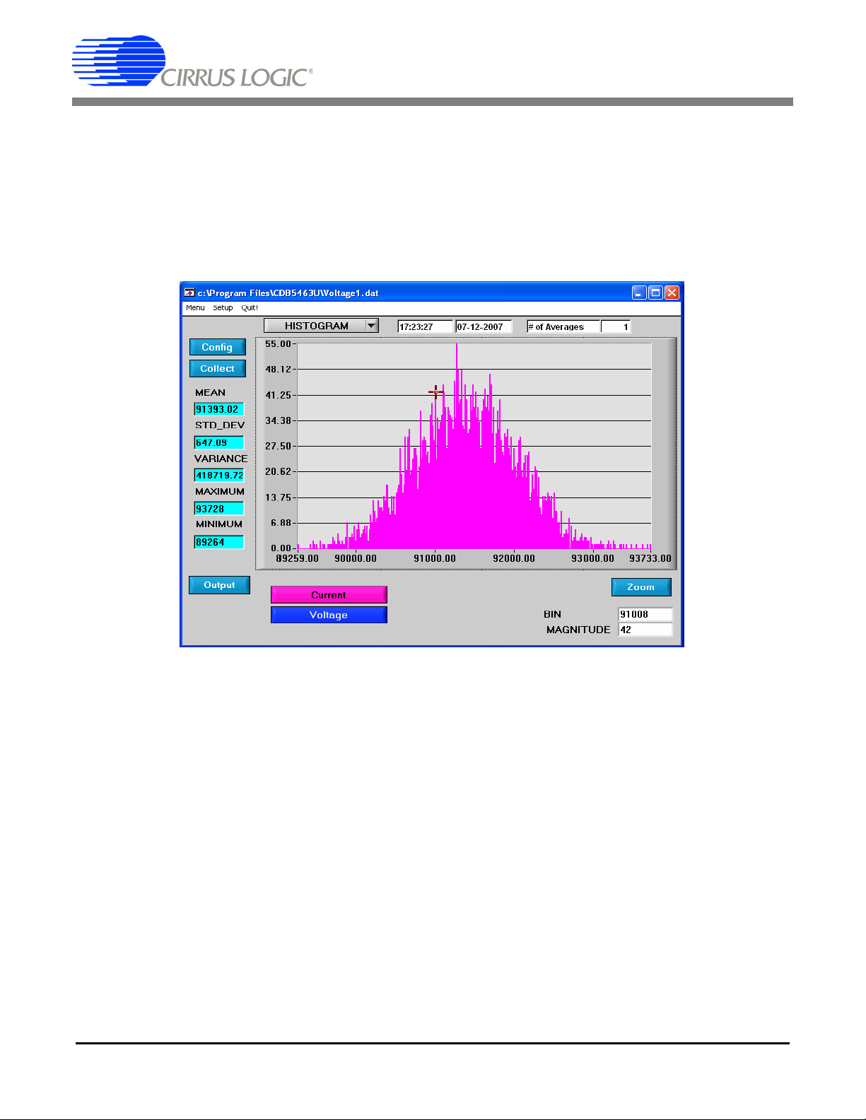
2.8.11 Histogram Information
The following is a description of the indicators associated with histogram analysis. Histograms can be plotted in the Data Collection Window by setting the analysis type pull-down menu to Histogram.
Figure 14. Histogram Analysis
2.8.11.1 BIN
Displays the x-axis value of the cursor on the histogram.
2.8.11.2 MAGNITUDE
Displays the y-axis value of the cursor on the histogram.
2.8.11.3 MEAN
Indicates the mean of the data sample set. The mean is calculated using the following formula:
n1–
Xi
∑
Mean
----------------=
i0=
n
22 DS805DB2
Page 23

CDB5463U
2.8.11.4 STD_DEV
Indicates the standard deviation of the collected data set. The standard deviation is calculated using the
following formula:
STDDEV
n1–
∑
i0=
=
------------------------------------------------
–
()
Xi
MEAN
2
n
2.8.11.5 VARIANCE
Indicates for the variance of the current data set. The variance is calculated using the following formula:
VARIANCE
n1–
i0=
------------------------------------------------=
∑
–
()
MEAN
Xi
2
n
2.8.11.6 MAXIMUM
Indicates the maximum value of the collected data set.
2.8.11.7 MINIMUM
Indicates the minimum value of the collected data set.
DS805DB2 23
Page 24

CDB5463U
2.8.12 Frequency Domain Information
The following describe the indicators associated with FFT (Fast Fourier Transform) analysis. FFT data
can be plotted in the Data Collection Window by setting the analysis type selector to FFT (Figure 15).
Figure 15. FFT Analysis
2.8.12.1 FREQUENCY
Displays the x-axis value of the cursor on the FFT display.
2.8.12.2 MAGNITUDE
Displays the y-axis value of the cursor on the FFT display.
2.8.12.3 S/PN
Indicates the signal-to-peak noise ratio (decibels).
2.8.12.4 SINAD
Indicates for the signal-plus-noise-plus-distortion to noise-plus-distortion ratio (decibels).
2.8.12.5 S/D
Indicates for the signal-to-distortion ratio, 4 harmonics are used in the calculations (decibels).
2.8.12.6 SNR
Indicates for the signal-to-noise ratio, first 4 harmonics are not included (decibels).
24 DS805DB2
Page 25

CDB5463U
2.8.12.7 FS-Pdb
Indicates for the full-scale to signal Ratio (decibels).
2.8.12.8 Time Domain Information
The following controls and indicators are associated with time domain analysis. Time domain data can be
plotted in the Data Collection Window by setting the analysis type selector to Time Domain (Figure 16).
Figure 16. Time Domain Analysis
2.8.12.9 COUNT
Displays current x-position of the cursor on the time domain display.
2.8.12.10 MAGNITUDE
Displays current y-position of the cursor on the time domain display.
2.8.12.11 MAXIMUM
Indicates for the maximum value of the collected data set.
2.8.12.12 MINIMUM
Indicates for the minimum value of the collected data set.
DS805DB2 25
Page 26

CDB5463U
2.9 EEPROM Window
CDB5463U has an "Auto-Boot" demo feature that uses the on-board serial EEPROM, so that the
CDB5463U can operate independently without being connected to a PC. CDB5463U GUI software also
provides an EEPROM Window for reading & writing the serial EEPROM (Figure 17).
Figure 17. EEPROM Window
2.9.1 Bytes to Read/Write
The Bytes to Read/Write field allows the user to define the number of bytes to read or write.
2.9.2 Read EEPROM
First input the number of bytes to read in the Bytes to Read/Write field. After pressing the Read button,
that number of bytes starting from the address 0x00 will be read from EEPROM and displayed in the EE-
PROM table in hexadecimal format.
2.9.3 Write EEPROM
Input the number of bytes to write in the Bytes to Read/Write field and input the hexadecimal byte values
in the EEPROM table starting from address 0x00. After pressing the Write button, the bytes in the EE-
PROM table will be written to the EEPROM.
26 DS805DB2
Page 27

CDB5463U
2.10 Debug Panel
The Debug panel provides the user a way to access CS5463 registers and send commands to CS5463
directly (Figure 18). Remember that the correct register page must be selected before accessing a register location. Refer to 5.15 in CS5463 data sheet for more details.
Figure 18. Debug Panel
DS805DB2 27
Page 28
APPENDIX A. BILL OF MATERIALS
0.25T TYPE E 24/19 BLU SQUIRES
ELEC. INC.
0.25T TYPE E 24/19 BLU SQUIRES
ELEC. INC.
CDB5463U
BILL OF MATERIAL (Page 1 of 2)
111-0103-001 REQUIRES WIRE, 1.5L X 0.25T X
111-0102-001 REQUIRES WIRE, 1.5L X 0.25T X
COMPONENTS
COMPONENTS
ED 100/2DS
TECHNOLOGY
TP-101-10
CORPORATION
DALE CRCW08052001F
R38
26 020-01588-01 A RES 10 OHM 1/8W ±1% 0805 FILM 1 R4 DALE CRCW080510R0F
27 020-01816-01 A RES 1k OHM 1/8W ±1% 0805 FILM 5 R5 R11 R12 R13 R18 DALE CRCW08051001F
28 020-01930-01 A RES 10k OHM 1/8W ±1% 0805 FILM 0 R19 DALE CRCW08051002F DO NOT POPULATE
29 035-00005-01 A RES POT, 5k ±10%, 25 TURN TRIMMING 0 R20 BOURNS 3296W-1-502 DO NOT POPULATE
30 020-01667-01 A RES 49.9 OHM 1/8W ±1% 0805 FILM 1 R21 DALE CRCW080549R9F
31 020-01905-01 A RES 6.04k OHM 1/8W ±1% 0805 FILM 0 R22 DALE CRCW08056041F DO NOT POPULATE
Item Cirrus P/N Rev Description Qty Reference Designator MFG MFG P/N Notes
1 001-06872-Z1 A CAP 0.1uF ±10% 50V NPb X7R 1206 6 C1 C18 C19 C21 C29 C30 KEMET C1206C104K5RAC
2 001-02779-01 A CAP 22pF ±5% 50V C0G 0805 1 C2 KEMET C0805C220J5GAC
CIRRUS LOGIC
CDB5463U_Rev_B.bom
3 001-02189-Z1 A CAP 0.1uF ±10% 16V X7R NPb 0603 5 C3 C4 C26 C32 C33 KEMET C0603C104K4RAC
4 012-00010-Z1 A CAP 47uF ±20% 16V NPb ELEC CASE C 4 C5 C8 C28 C31 PANASONIC EEE1CA470WR
5 001-04344-01 A CAP 0.1uF ±5% 50V X7R 0805 7 C6 C7 C10 C11 C12 C15 C25 KEMET C0805C104J5RAC
6 001-03266-01 A CAP 220pF ±10% 50V X7R 0805 4 C9 C17 C20 C24 KEMET C0805C221K5RAC
7 001-06685-01 A CAP 0.018uF ±10% 50V X7R 1206 2 C13 C23 KEMET C1206C183K5RAC
8 012-00012-01 A CAP 10uF ±20% 16V ELEC CASE A 3 C14 C22 C1000 PANASONIC ECEV1CS100SR
9 001-07078-01 A CAP 1uF ±10% 25V X7R 1206 1 C16 KEMET C1206C105K3RAC
10 070-00055-01 A DIODE ARRAY 5V (TVS) ESD SOT143 1 D1 LITTLE FUSE SP0503BAHT
11 165-00004-01 A LED CLR SUP RED 1.7V 1mA 1.6MCD SMD 6 D2 D3 D4 D5 D6 D7 CHICAGO MINIATURE CMD28-21SRC/TR8/T1
12 115-00003-01 A HDR 5x2 MLE .1"CTR S GLD 1 J1 SAMTEC TSW-105-07-G-D
13 110-00041-01 A CON RA USB BLK 1 J2 AMP 787780-1
14 110-00010-01 A CON BPOST 2" SILV NYLON INS RED 3 J3 J5 J6 JOHNSON
15 110-00008-01 A CON BPOST 2" SILV NYLON INS BLK 1 J4 JOHNSON
16 115-00016-01 A HDR 3x2 MLE .1"CTR .062BD S GLD 6 J8 J9 J17 J22 J24 J26 SAMTEC TSW-103-07-G-D
20 110-00055-01 A CON TERM BLOCK 4 POS 5mm C/C BLUE 2 J23 J27 OST ED 100/4DS
17 115-00014-01 A HDR 2x1 ML .1"CTR 062BD ST GLD TH 5 J10 J13 J15 J16 J18 SAMTEC TSW-102-07-G-S
18 115-00013-01 A HDR 2x2 MLE .1"CTR .062BD S GLD 1 J12 SAMTEC TSW-102-07-G-D
19 110-00056-01 A CON TERM BLOCK 2 POS 5mm C/C BLUE 1 J14 ON-SHORE
24 304-00001-01 A SPCR, STANDOFF 4-40 THR, 0.875"L 4 MH1 MH2 MH3 MH4 KEYSTONE 1809 REQUIRES 4-40- PAN HEAD SCREW
21 115-00009-01 A HDR 3x1 ML .1"CTR 062BD ST GLD TH 1 J25 SAMTEC TSW-103-07-G-S
22 115-00031-01 A HDR 11x2 MLE .1"CTR S GLD 1 J40 SAMTEC TSW-111-07-G-D
25 020-01848-01 A RES 2k OHM 1/8W ±1% 0805 FILM 12 R2 R3 R6 R7 R8 R14 R15 R16 R17 R29 R36
23 080-00004-01 A WIRE, JUMPER 2P, 0.1"CTR, BRASS 6 JP1 JP2 JP3 JP4 JP5 JP6 COMPONENTS
32 021-00759-01 A RES 1k OHM 1/3W ±5% 1210 FILM 4 R23 R24 R26 R28 DALE CRCW1210102J
28 DS805DB2
Page 29

CDB5463U
DALE CRCW0805000Z
BILL OF MATERIAL (Page 2 of 2)
R61 R62
ASSEMBLED
ASSEMBLED
NC7SZ04M5X
74LCX760WM
KEYSTONE 5001
TP22 TP23 TP24 TP25 TP26 TP27 TP30
NC7WZ07P6X
SEMICONDUCTOR
SEMICONDUCTOR
ASSEMBLED
NC7SB3157P6X
SEMICONDUCTOR
SEMICONDUCTOR
603-00176-01
PER ASSY DWG 603-00176-01
49 062-00122-01 A IC PGM EEPROM 512x8 4K SPI SOIC8 1 U10 ATMEL AT25040AN-10SI-2.7 NOT PROGRAMMED BEFORE
50 080-00003-01 A WIRE BPOST 1.5X.25" 24/19 GA BLU 4 XJ3XJ4 XJ5 XJ6 SQUIRES L-1.5X.25TX.25T_TYPE_E_ WIRES FOR BINDING POSTS
51 300-00001-01 A SCREW 4-40X5/16" PH STEEL 4 XMH1 XMH2 XMH3 XMH4 BUILDING FASTENERS PMS 440 0031 PH SCREWS FOR STANDOFFS
52 135-00013-01 A SKT PINCH CONTACT FOR SSOP24 0 XU6 ENPLAS OTS-2434-0.65-01 DO NOT POPULATE
53 312-00008-01 A INSULATOR .312 x .145 FOR HC49U/US 1 XY1 ECS 700-9001 INSULATOR FOR Y1
54 100-00049-01 A XTL OSC 4.0960MHZ HC49S 50ppm 50pF 1 Y1 CAL CRYSTAL CCL-6S-4.0960C14F REQUIRES INSULATOR XY1
55 070-00006-01 A DIODE TR 6.8V 600W AXL 3 Z1 Z2 Z3 LITTLE FUSE P6KE6.8
56 110-00013-Z1 D CON SHUNT 2P .1"CTR BLK NPb 12 MOLEX 15-29-1025 INSTALL SHUNTS PER ASSY DWG
57 422-00037-01 A1 LBL SUBASSY PRODUCT NUMBER 1 CIRRUS LOGIC 422-00037-01 PLACE PRODUCT NUMBER LABEL
58 240-00176-Z1 B PCB CDB5460A_61A_63 1 CIRRUS LOGIC 240-00176-Z1
59 603-00176-01 B ASSY DWG PWA CDB5460A_61A_63 REF CIRRUS LOGIC 603-00176-01
60 600-00176-01 B SCHEM CDB5460A_61A_63 REF CIRRUS LOGIC 600-00176-01
61 020-01473-01 A RES 0 OHM 1/18W ±1% 0805 FILM 0 R34 DALE CRCW0805000Z DO NOT POPULATE
Item Cirrus P/N Rev Description Qty Reference Designator MFG MFG P/N Notes
33 020-03355-01 A RES 301 OHM 1/3W ±1% 1210 FILM 1 R25 DALE CRCW12103010F
34 020-03378-01 A RES 470 OHM 1/3W ±1% 1210 FILM 4 R30 R31 R32 R33 DALE CRCW12104700F
CIRRUS LOGIC
CDB5463U_Rev_B.bom
35 020-03539-01 A RES 12.1k OHM 1/3W ±1% 1210 FILM 1 R35 DALE CRCW12101212F
43 062-00079-01 A IC PGM USB 16kB FLASH MCU LQFP32 1 U3 CYGNAL C8051F320 NOT PROGRAMMED BEFORE
44 060-00061-01 A IC LNR PRECISION V REF 2.5V SO8 1 U4 LINEAR TECH LT1019CS8-2.5
41 062-00124-01 A IC PGM 128 BIT SER EEPROM SOT23-5 1 U1 MICROCHIP 24LC00-I/OT NOT PROGRAMMED BEFORE
38 020-02273-Z1 A RES 0 OHM 1/4W NPb 1206 FILM 1 R64 DALE CRCW12060000Z0EA
39 120-00002-01 A SWT 0/1 TACT W/ESD 1 S1 C&K PTS645TL50 INSTALL AFTER WASH PROCESS
36 020-02748-01 A RES 15k OHM 1/8W ±1% 1206 FILM 1 R37 DALE CRCW12061502F
37 020-01473-01 A RES 0 OHM 1/18W ±1% 0805 FILM 12 R51 R52 R53 R54 R55 R56 R57 R58 R59 R60
42 061-00250-01 A IC DIG LOW V BUF/LDRV 5V OPEN DRAIN 1 U2 FAIRCHILD
40 110-00045-01 A CON TEST PT .1"CTR TIN PLATE BLK 16 TP1 TP2 TP9 TP10 TP11 TP12 TP13 TP20 TP21
45 061-00190-01 A IC LOG, UHS TINY, DUAL BUF, SC70-6 1 U5 FAIRCHILD
48 061-00219-01 A IC LOG UHS TINY ANALOG SWT 6P SC70 2 U9 U11 FAIRCHILD
46 065-00162-Z3 C IC CRUS PWR/ENERGY MON NPb SSOP24 1 U6 CIRRUS LOGIC CS5463-ISZ/C
47 061-00002-01 A IC LOG INV 5P UHS TINY SOT23 1 U8 FAIRCHILD
62 110-00045-01 A CON TEST PT .1"CTR TIN PLATE BLK 0 TP7 TP8 KEYSTONE 5001 DO NOT POPULATE
DS805DB2 29
Page 30

APPENDIX B. SCHEMATICS
CDB5463U
Figure 19. Schematic - Analog Inputs
30 DS805DB2
Page 31

CDB5463U
Figure 20. Schematic - CS5463 & Socket
DS805DB2 31
Page 32
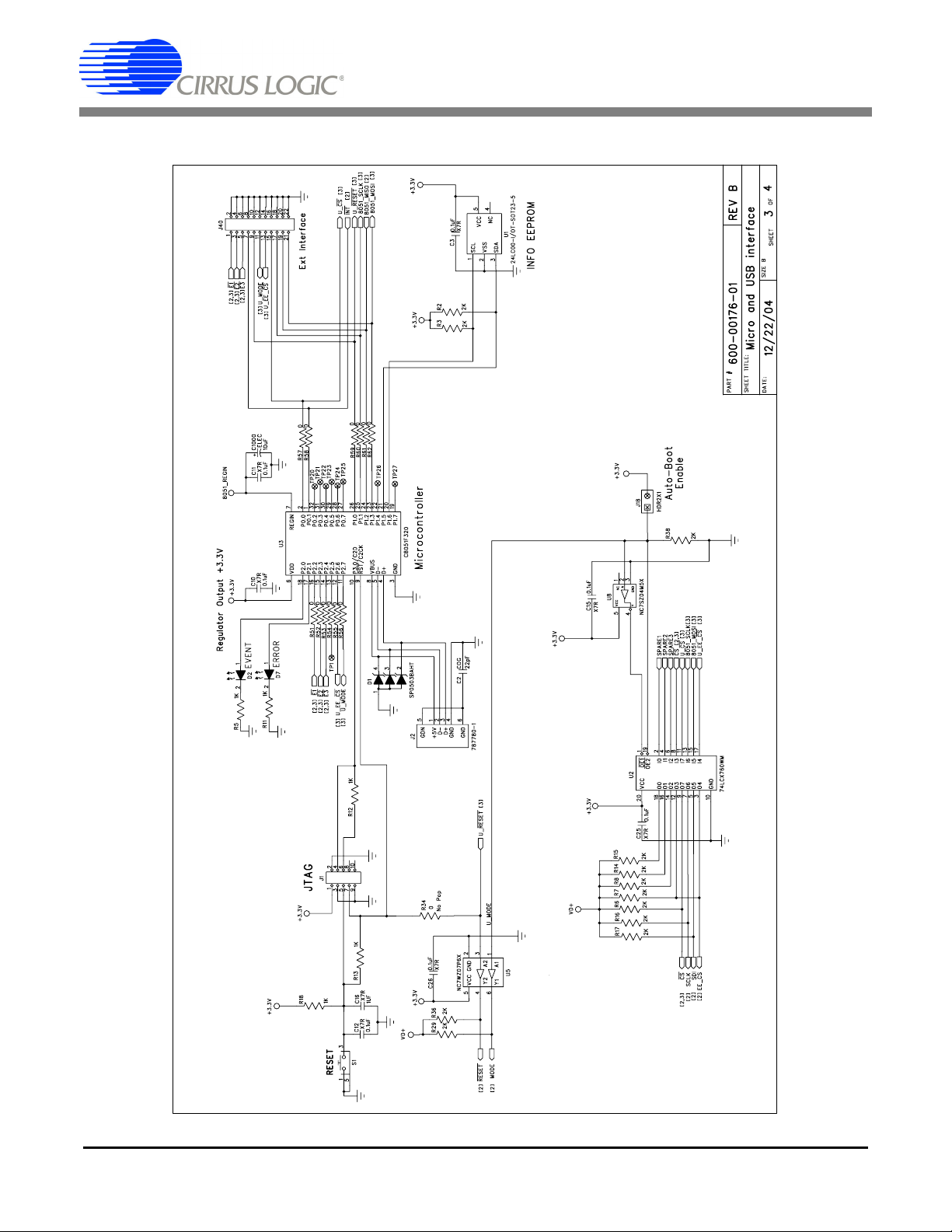
CDB5463U
Figure 21. Schematic - Microcontroller & USB Interface
32 DS805DB2
Page 33

CDB5463U
Figure 22. Schematic - Power Supplies
DS805DB2 33
Page 34
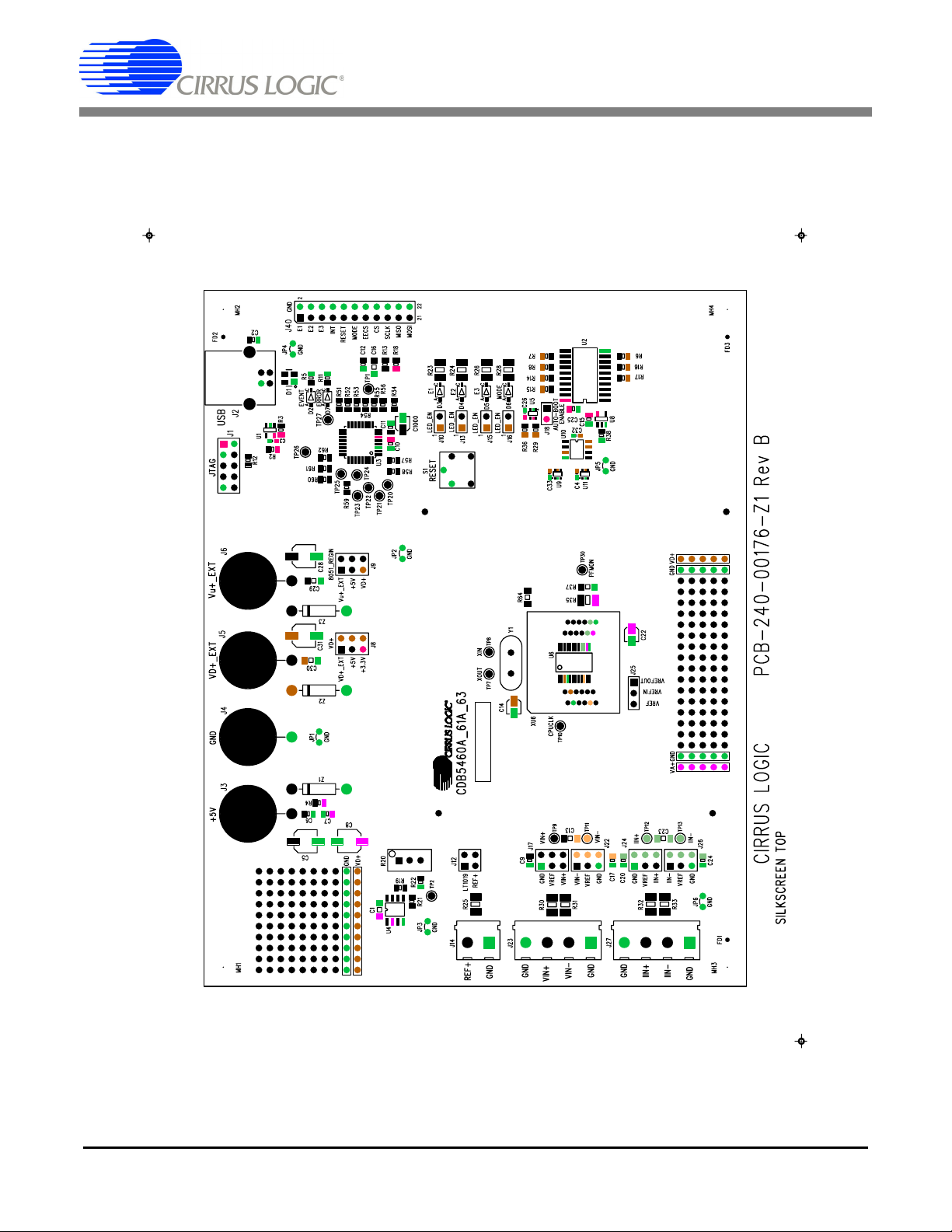
APPENDIX C. LAYER PLOTS
CDB5463U
Figure 23. Top Silkscreen
34 DS805DB2
Page 35

CDB5463U
Figure 24. Top Routing
DS805DB2 35
Page 36

CDB5463U
Figure 25. Bottom Routing
36 DS805DB2
Page 37

CDB5463U
Figure 26. Bottom Silkscreen
DS805DB2 37
Page 38

REVISION HISTORY
Revision Date Changes
DB1 SEP 2007 Initial Release.
DB2 OCT 2007 Minor correction to List of Figures.
CDB5463U
Contacting Cirrus Logic Support
For all product questions and inquiries contact a Cirrus Logic Sales Representative. To find the one nearest to you
go to www.cirrus.com
IMPORTANT NOTICE
Cirrus Logic, Inc. and its subsidiaries ("Cirrus") believe that the information contained in this document is accurate and reliable. However, the information is subject
to change without notice and is provided "AS IS" without warranty of any kind (express or implied). Customers are advised to obtain the latest version of relevant
information to verify, before placing orders, that information being relied on is current and complete. All products are sold subject to the terms and conditions of sale
supplied at the time of order acknowledgment, including those pertaining to warranty, indemnification, and limitation of liability. No responsibility is assumed by Cirrus
for the use of this information, including use of this information as the basis for manufacture or sale of any items, or for infringement of patents or other rights of third
parties. This document is the property of Cirrus and by furnishing this information, Cirrus grants no license, express or implied under any patents, mask work rights,
copyrights, trademarks, trade secrets or other intellectual property rights. Cirrus owns the copyrights associated with the information contained herein and gives
consent for copies to be made of the information only for use within your organization with respect to Cirrus integrated circuits or other products of Cirrus. This consent does not extend to other copying such as copying for general distribution, advertising or promotional purposes, or for creating any work for resale.
CERTAIN APPLICATIONS USING SEMICONDUCTOR PRODUCTS MAY INVOLVE POTENTIAL RISKS OF DEATH, PERSONAL INJURY, OR SEVERE PROPERTY OR ENVIRONMENTAL DAMAGE ("CRITICAL APPLICATIONS"). CIRRUS PRODUCTS ARE NOT DESIGNED, AUTHORIZED OR WARRANTED FOR
USE IN AIRCRAFT SYSTEMS, MILITARY APPLICATIONS, PRODUCTS SURGICALLY IMPLANTED INTO THE BODY, AUTOMOTIVE SAFETY OR SECURITY
DEVICES, LIFE SUPPORT PRODUCTS OR OTHER CRITICAL APPLICATIONS. INCLUSION OF CIRRUS PRODUCTS IN SUCH APPLICATIONS IS UNDERSTOOD TO BE FULLY AT THE CUSTOMER'S RISK AND CIRRUS DISCLAIMS AND MAKES NO WARRANTY, EXPRESS, STATUTORY OR IMPLIED, INCLUDING THE IMPLIED WARRANTIES OF MERCHANTABILITY AND FITNESS FOR PARTICULAR PURPOSE, WITH REGARD TO ANY CIRRUS PRODUCT THAT
IS USED IN SUCH A MANNER. IF THE CUSTOMER OR CUSTOMER'S CUSTOMER USES OR PERMITS THE USE OF CIRRUS PRODUCTS IN CRITICAL
APPLICATIONS, CUSTOMER AGREES, BY SUCH USE, TO FULLY INDEMNIFY CIRRUS, ITS OFFICERS, DIRECTORS, EMPLOYEES, DISTRIBUTORS AND
OTHER AGENTS FROM ANY AND ALL LIABILITY, INCLUDING ATTORNEYS' FEES AND COSTS, THAT MAY RESULT FROM OR ARISE IN CONNECTION
WITH THESE USES.
Cirrus Logic, Cirrus, and the Cirrus Logic logo designs are trademarks of Cirrus Logic, Inc. All other brand and product names in this document may be trademarks
or service marks of their respective owners.
LabWindows and CVI are registered trademarks of National Instruments, Inc.
Windows, Windows 2000, and Windows XP are trademarks or registered trademarks of Microsoft Corporation.
PADS and PowerLogic are trademarks of Mentor Graphics Corporation.
38 DS805DB2
 Loading...